EP4142128B1 - Voltage converter, power supply and method of controlling voltage converter - Google Patents
Voltage converter, power supply and method of controlling voltage converter Download PDFInfo
- Publication number
- EP4142128B1 EP4142128B1 EP22192618.1A EP22192618A EP4142128B1 EP 4142128 B1 EP4142128 B1 EP 4142128B1 EP 22192618 A EP22192618 A EP 22192618A EP 4142128 B1 EP4142128 B1 EP 4142128B1
- Authority
- EP
- European Patent Office
- Prior art keywords
- voltage
- voltage converter
- converter
- proportional coefficient
- signal
- Prior art date
- Legal status (The legal status is an assumption and is not a legal conclusion. Google has not performed a legal analysis and makes no representation as to the accuracy of the status listed.)
- Active
Links
Images


Classifications
-
- H—ELECTRICITY
- H02—GENERATION; CONVERSION OR DISTRIBUTION OF ELECTRIC POWER
- H02M—APPARATUS FOR CONVERSION BETWEEN AC AND AC, BETWEEN AC AND DC, OR BETWEEN DC AND DC, AND FOR USE WITH MAINS OR SIMILAR POWER SUPPLY SYSTEMS; CONVERSION OF DC OR AC INPUT POWER INTO SURGE OUTPUT POWER; CONTROL OR REGULATION THEREOF
- H02M3/00—Conversion of DC power input into DC power output
- H02M3/02—Conversion of DC power input into DC power output without intermediate conversion into AC
- H02M3/04—Conversion of DC power input into DC power output without intermediate conversion into AC by static converters
- H02M3/10—Conversion of DC power input into DC power output without intermediate conversion into AC by static converters using discharge tubes with control electrode or semiconductor devices with control electrode
- H02M3/145—Conversion of DC power input into DC power output without intermediate conversion into AC by static converters using discharge tubes with control electrode or semiconductor devices with control electrode using devices of a triode or transistor type requiring continuous application of a control signal
- H02M3/155—Conversion of DC power input into DC power output without intermediate conversion into AC by static converters using discharge tubes with control electrode or semiconductor devices with control electrode using devices of a triode or transistor type requiring continuous application of a control signal using semiconductor devices only
- H02M3/156—Conversion of DC power input into DC power output without intermediate conversion into AC by static converters using discharge tubes with control electrode or semiconductor devices with control electrode using devices of a triode or transistor type requiring continuous application of a control signal using semiconductor devices only with automatic control of output voltage or current, e.g. switching regulators
- H02M3/158—Conversion of DC power input into DC power output without intermediate conversion into AC by static converters using discharge tubes with control electrode or semiconductor devices with control electrode using devices of a triode or transistor type requiring continuous application of a control signal using semiconductor devices only with automatic control of output voltage or current, e.g. switching regulators including plural semiconductor devices as final control devices for a single load
- H02M3/1584—Conversion of DC power input into DC power output without intermediate conversion into AC by static converters using discharge tubes with control electrode or semiconductor devices with control electrode using devices of a triode or transistor type requiring continuous application of a control signal using semiconductor devices only with automatic control of output voltage or current, e.g. switching regulators including plural semiconductor devices as final control devices for a single load with a plurality of power processing stages connected in parallel
-
- H—ELECTRICITY
- H02—GENERATION; CONVERSION OR DISTRIBUTION OF ELECTRIC POWER
- H02J—ELECTRIC POWER NETWORKS; CIRCUIT ARRANGEMENTS OR SYSTEMS FOR SUPPLYING OR DISTRIBUTING ELECTRIC POWER; SYSTEMS FOR STORING ELECTRIC ENERGY
- H02J1/00—Circuit arrangements for DC mains or DC distribution networks
- H02J1/10—Parallel operation of DC sources
- H02J1/102—Parallel operation of DC sources being switching converters
-
- H—ELECTRICITY
- H02—GENERATION; CONVERSION OR DISTRIBUTION OF ELECTRIC POWER
- H02M—APPARATUS FOR CONVERSION BETWEEN AC AND AC, BETWEEN AC AND DC, OR BETWEEN DC AND DC, AND FOR USE WITH MAINS OR SIMILAR POWER SUPPLY SYSTEMS; CONVERSION OF DC OR AC INPUT POWER INTO SURGE OUTPUT POWER; CONTROL OR REGULATION THEREOF
- H02M1/00—Details of apparatus for conversion
- H02M1/0003—Details of control, feedback or regulation circuits
- H02M1/0025—Arrangements for modifying reference values, feedback values or error values in the control loop of a converter
Definitions
- the present disclosure relates to a field of power supplies, and more particularly, to a a power supply and a method of controlling a voltage converter.
- An active current sharing method is widely used in direct current/alternating current (AC/DC) and DC/DC converter redundant operations. Outputs of a plurality of voltage converters are connected together, so that a total output power of the converters meets power requirements of an application in a case of power redundancy.
- the voltage converters involved in the current sharing method may include a master voltage converter and one or more slave voltage converters.
- a master-slave exchange may frequently occur for various reasons (for example, performance parameters of the various voltage converters involved are inconsistent).
- RAJAGOPALAN J ET AL "Modeling and dynamic analysis of paralleled DC/DC converters with master-slave current sharing control", APPLIED POWER ELECTRONICS CONFERENCE AND EXPOSITION, 1996.
- a power supply and a method of controlling a voltage converter are provided.
- the invention is defined by the appended claims.
- the adjustable first proportional coefficient is selected based on whether the voltage converter is a master voltage converter or a slave voltage converter in a current sharing mode, so that a magnitude of the generated first voltage signal may be selected according to a role of the voltage converter in a master-slave current sharing mode, which makes it more difficult, for example, for a magnitude of a first voltage signal of the slave voltage converter to exceed a magnitude of a first voltage signal of the master voltage converter, and thus reduces a frequency of master-slave exchange.
- the techniques of the present disclosure may be implemented in a form of hardware and/or software (including a firmware, a microcode, etc.).
- the techniques of the present disclosure may take a form of a computer program product on a computer-readable medium having stored instructions for use by or in conjunction with an instruction execution system.
- the computer-readable medium may be any medium that may contain, store, communicate, propagate, or transmit instructions.
- the computer-readable medium may include, but is not limited to, electrical, magnetic, optical, electromagnetic, infrared, or semiconductor systems, apparatus, devices, or propagation mediums.
- the computer-readable medium include: a magnetic storage device, such as a magnetic tape or hard disk (HDD); an optical storage device, such as a compact disk (CD-ROM); a memory, such as a random access memory (RAM) or flash memory; and/or a wired /wireless communication link.
- a magnetic storage device such as a magnetic tape or hard disk (HDD)
- an optical storage device such as a compact disk (CD-ROM)
- a memory such as a random access memory (RAM) or flash memory
- RAM random access memory
- FIG. 1 shows a schematic diagram of a voltage feedback converter.
- the voltage feedback converter has a voltage controller loop.
- An output Vout of the converter is amplified by an amplifier with a coefficient H, and then subtracted from a reference signal Vref to generate an error signal Verr.
- the error signal Verr is inputted to a proportional-integral-derivative (PID) controller or pole/zero controller to produce a control signal for regulating the output of the converter.
- PID proportional-integral-derivative
- the output of the converter passes through a unidirectionally conductive device (diode/rectifier/MOSFET) before flowing into the amplifier with the coefficient H.
- I_MARGIN is a predefined output current difference, which means that a current with a difference within I MARGIN is not considered to have a substantial difference in the technical solutions of the present disclosure.
- Vlshare K x Iout_master
- Ierr_mater -I_MARGIN.
- an output current of the converter is less than that of the master voltage converter.
- Ierr_slave Iout_master-(Iout_slave + I_MARGIN) will be greater than 0.
- Iout_master-Iout_slave I_MARGIN, then Ierr_slave will be equal to 0, and DeltaV_slave will also be equal to 0.
- the output current of the slave voltage converter will change as an output current of the master voltage converter changes, in this case,
- Iout_slave When the output current of the converter oscillates, Iout_slave may temporarily be higher than Iout_master, and leads to an exchange of master/slave roles. In this case, it may be difficult to settle the oscillation because the converters are all temporarily acting as slave voltage converters and trying to adjust their own output. In some solutions, the situation may be improved by increasing a value of I_MARGIN. With the larger value of I_MARGIN, the difference between Iout_slave and Iout_master should be larger to realize a master-slave exchange. However, it is found that the solution may lead to difficulties in meeting current sharing accuracy requirements.
- the present disclosure proposes a power supply and a method of controlling said power supply.
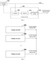
- FIG. 3 shows a schematic structural diagram of a voltage converter according to the embodiments of the present disclosure.
- a voltage converter 300 includes a converter module 310, a current sharing terminal 320 and a control circuit 330.
- the converter module 310 converts an input voltage to an output voltage.
- the current sharing terminal 320 is connected in parallel with a current sharing terminal of each of at least one other voltage converter.
- the control circuit 330 generates a first voltage signal proportional to an output current of the converter module 310 with an adjustable first proportional coefficient and outputs the first voltage signal to the current sharing terminal 320; wherein the first proportional coefficient is selected based on whether the voltage converter 300 is a master voltage converter or a slave voltage converter in a current sharing state; generates a first current signal proportional to a second voltage signal at the current sharing terminal 320 with a second proportional coefficient, wherein the second voltage signal is a largest voltage signal among the first voltage signal and other voltage signal from each current sharing terminal connected in parallel, and the first proportional coefficient is less than or equal to a reciprocal of the second proportional coefficient; subtracts the output current of the converter module 310 from the first current signal so as to generate an error current signal; and adjusts the output voltage of the converter module 310 based on the error current signal.
- subtracting the output current of the converter module 310 from the first current signal so as to generate an error current signal may include: subtracting the output current of the converter module 310 and a margin current from the first current signal so as to generate the error current signal.
- control circuit 330 may further include a comparison circuit 331.
- the comparison circuit 331 compares the first voltage signal with the second voltage signal, and outputs the larger one of the first voltage signal and the second voltage signal as a new second voltage signal.
- the control circuit 330 may include at least one amplifier 332 having different amplification coefficients; and a selector 333 configured to select one of the at least one amplifier so as to generate the first voltage signal.
- one of the amplifiers 332 corresponds to a role of master voltage converter, and at least one of the amplifiers 332 corresponds to a role of slave voltage converter.
- the selector 333 selects an amplifier or amplification coefficient to be used based on whether the voltage converter 300 is a master voltage converter or a slave voltage converter.
- the value of the first proportional coefficient is less than the reciprocal value of the second proportional coefficient; and when the voltage converter 300 is the master voltage converter, the value of the first proportional coefficient is equal to the reciprocal value of the second proportional coefficient.
- the value of the first proportional coefficient may be in a range of 0.5 times to 0.6 times the reciprocal value of the second proportional coefficient.
- the value range may also change. Such a change shall fall within the scope of the technical solutions of the present disclosure.
- a ratio of the value of the first proportional coefficient to the reciprocal value of the second proportional coefficient may be reduced.
- a ratio of the value of the first proportional coefficient to the reciprocal value of the second proportional coefficient is increased.
- FIG. 4 shows a schematic arrangement of a power supply according to the embodiments.
- a current sharing power supply 400 is formed by connecting respective current sharing terminals of a plurality of voltage converters 300 in parallel with each other.
- FIG. 5 shows a method 500 of controlling a voltage converter corresponding to the voltage converter 300 shown in FIG. 3 .
- the voltage converter 300 includes a converter module 310 configured to convert an input voltage to an output voltage, a current sharing terminal 320 configured to be connected in parallel with a current sharing terminal of each of at least one other voltage converter, and a control circuit 330.
- the method 500 is performed by the control circuit 330 and includes steps S510 to S540.
- step S510 a first voltage signal proportional to an output current of the converter module 310 with an adjustable first proportional coefficient is generated and output to the current sharing terminal 320.
- the first proportional coefficient is selected based on whether the voltage converter 300 is a master voltage converter or a slave voltage converter in a current sharing mode.
- step S520 a first current signal proportional to a second voltage signal at the current sharing terminal 320 with a second proportional coefficient is generated.
- the second voltage signal is a largest voltage signal among the first voltage signal and other voltage signal from each current sharing terminal connected in parallel, and the first proportional coefficient is less than or equal to a reciprocal of the second proportional coefficient.
- step S530 the output current of the converter module 310 is subtracted from the first current signal so as to generate an error current signal.
- step S540 the output voltage of the converter module 310 is adjusted based on the error current signal.
- the adjustable first proportional coefficient is adjusted based on whether the voltage converter 300 is a master voltage converter or a slave voltage converter in a current sharing mode, so that a magnitude of the generated first voltage signal may be selected according to a role of the voltage converter 300 in a master-slave current sharing mode, which makes it more difficult, for example, for a magnitude of a first voltage signal of the slave voltage converter to exceed a magnitude of a first voltage signal of the master voltage converter, and thus reduces a frequency of master-slave exchange.
- subtracting the output current of the converter module 310 from the first current signal so as to generate an error current signal may include: subtracting the output current of the converter module 310 and a margin current from the first current signal so as to generate the error current signal.
- the method 500 may further include: comparing the first voltage signal with the second voltage signal, and outputting the larger one of the first voltage signal and the second voltage signal as a new second voltage signal.
- the step may be performed by a comparison circuit 331.
- the control circuit 330 may include at least one amplifier 332 having different amplification coefficients.
- the method 500 may include selecting one of the at least one amplifier having different amplification coefficients so as to generate the first voltage signal.
- the step may be performed, for example, by a selector 333.
- one of the amplifiers 332 corresponds to a role of master voltage converter and at least one of the amplifiers 332 corresponds to a role of slave voltage converter.
- the selector 333 selects an amplifier or amplification coefficient to be used based on whether the voltage converter 300 is a master voltage converter or a slave voltage converter.
- the value of the first proportional coefficient is less than the reciprocal value of the second proportional coefficient; and when the voltage converter 300 is the master voltage converter, the value of the first proportional coefficient is equal to the reciprocal value of the second proportional coefficient.
- the value of the first proportional coefficient may be in a range of 0.5 times to 0.6 times the reciprocal value of the second proportional coefficient.
- the value range may also change. Such a change shall fall within the scope of the technical solutions of the present disclosure.
- a ratio of the value of the first proportional coefficient to the reciprocal value of the second proportional coefficient is reduced.
- a ratio of a value of the first proportional coefficient to a reciprocal value of the second proportional coefficient is increased.
- FIG. 6 shows a method 600 of designing a power supply corresponding to the power supply of FIG. 4 .
- the method 600 may include step S610 of connecting current sharing terminals 320 of a plurality of voltage converters 300 controlled according to the method shown in FIG. 5 in parallel with each other.
- the first voltage signal is calculated by setting DeltaV to be greater than 0 and selecting another value of K with DeltaV as a control signal.
- a lower (even 0) gain K' is selected so that K' x Iout_slave will not be higher than K x Iout_master, and Vlshare is always equal to K x Iout_master.
- the first voltage signal is calculated by setting DeltaV to be 0 and selecting K with DeltaV as a control signal.
- the situation of FIG. 7 is the same as that of FIG. 2 .
- K' x Iout_slave of the slave voltage converter will not be higher than K x Iout_master, so that the master/slave roles may not be changed easily even under a dynamic load condition.
- a value of K' may be determined according to specific implementations.
- K' When the value of K' is too small (e.g., much less than K), the master/slave roles of the voltage converter are indeed not easily changed. In this case, however, when a voltage converter exits from the role of master voltage converter, it may take a long time for another voltage converter (which operates as a slave voltage converter) to become a master voltage converter.
- K' When the value of K' is too large (e.g., close to K), an effect of avoiding a frequent master-slave switching may not be apparent.
- the value of K' may be adjusted according to a current working condition of the power supply. For example, when a master-slave conversion occurs frequently in the voltage converter, it is indicated that the value of K' may be too large at present, and a frequency of the master-slave conversion may be reduced by lowering the value of K'.
- a slave-master conversion occurs, if a conversion speed of the voltage converter is slow, for example, no voltage converter may become the master voltage converter for a long time, the conversion speed may be increased by increasing the value of K'.
- the value of K' of each voltage converter that performs a current sharing in the power supply may be adjusted in any suitable manner.
- the value of K' of each voltage converter may be controlled by a centralized (micro) controller according to a working condition of the power supply by means of centralized control.
- a greater K' value may be assigned (or preferentially adjusted) to a voltage converter with better and/or more stable performances, so that the voltage converter may have a greater chance of being the master voltage converter.
- a corresponding amplifier/first proportional coefficient/amplifier gain may be selected by means of a selection switch.
- the selection switch may be implemented, for example, in one or more of the following ways.
Landscapes
- Engineering & Computer Science (AREA)
- Power Engineering (AREA)
- Dc-Dc Converters (AREA)
Description
- The present disclosure relates to a field of power supplies, and more particularly, to a a power supply and a method of controlling a voltage converter.
- An active current sharing method is widely used in direct current/alternating current (AC/DC) and DC/DC converter redundant operations. Outputs of a plurality of voltage converters are connected together, so that a total output power of the converters meets power requirements of an application in a case of power redundancy.
- The voltage converters involved in the current sharing method may include a master voltage converter and one or more slave voltage converters. In a practical application, a master-slave exchange may frequently occur for various reasons (for example, performance parameters of the various voltage converters involved are inconsistent).
- Therefore, a technology that may solve frequent master-slave exchanges is required.
- RAJAGOPALAN J ET AL: "Modeling and dynamic analysis of paralleled DC/DC converters with master-slave current sharing control", APPLIED POWER ELECTRONICS CONFERENCE AND EXPOSITION, 1996. APEC '96. CONFERENCE PROCEEDINGS 1996., ELEVENTH ANNUAL SAN JOSE, CA, USA 3-7 MARCH 1996, NEW YORK, NY, USA, IEEE, US, vol. 2, 3 March 1996 (1996-03-03), pages 678-684, XP010159857, DOI: 10.1109/APEC. 1996.500513 ISBN: 978-0-7803-3044-3 discloses modeling and dynamic analysis of paralleled dc/dc converters with master-slave current sharing control.
- According to the embodiments of the present disclosure, a power supply and a method of controlling a voltage converter are provided. The invention is defined by the appended claims.
- The adjustable first proportional coefficient is selected based on whether the voltage converter is a master voltage converter or a slave voltage converter in a current sharing mode, so that a magnitude of the generated first voltage signal may be selected according to a role of the voltage converter in a master-slave current sharing mode, which makes it more difficult, for example, for a magnitude of a first voltage signal of the slave voltage converter to exceed a magnitude of a first voltage signal of the master voltage converter, and thus reduces a frequency of master-slave exchange.
- Other advantages may be apparent to those skilled in the art. Some embodiments may not have the advantages, or have some or all of the advantages.
- The embodiments of the present disclosure and the features and advantages thereof may be understood more completely through the following description in conjunction with the accompanying drawings.
-
FIG. 1 shows a schematic diagram of a voltage feedback converter. -
FIG. 2 shows a schematic diagram of another voltage feedback converter. -
FIG. 3 shows a schematic structural diagram of a voltage converter according to the embodiments of the present disclosure. -
FIG. 4 shows a schematic arrangement of a power supply according to the embodiments. -
FIG. 5 shows a method of controlling a voltage converter corresponding to the voltage converter shown inFIG. 3 . -
FIG. 6 shows a method of designing a power supply corresponding to the power supply ofFIG. 4 . -
FIG. 7 shows a schematic circuit diagram of a voltage converter according to the embodiments of the present disclosure. - The embodiments of the present disclosure will be described below with reference to the accompanying drawings. It should be understood, however, that the descriptions are exemplary only, and are not intended to limit the scope of the present disclosure. In addition, in the following description, descriptions of well-known structures and techniques are omitted to avoid unnecessarily obscuring the concepts of the present disclosure.
- Some block diagrams and/or flow diagrams are shown in the accompanying drawings. It will be understood that some blocks or combinations thereof in the block diagrams and/or flowcharts may be implemented by computer program instructions. The computer program instructions may be provided to a processor of a general-purpose computer, a dedicated-purpose computer, or other programmable data processing apparatus, so that the instructions, when executed by the processor, may create means for implementing the functions/operations illustrated in the block diagrams and/or flow diagrams.
- Accordingly, the techniques of the present disclosure may be implemented in a form of hardware and/or software (including a firmware, a microcode, etc.). In addition, the techniques of the present disclosure may take a form of a computer program product on a computer-readable medium having stored instructions for use by or in conjunction with an instruction execution system. In the context of the present disclosure, the computer-readable medium may be any medium that may contain, store, communicate, propagate, or transmit instructions. For example, the computer-readable medium may include, but is not limited to, electrical, magnetic, optical, electromagnetic, infrared, or semiconductor systems, apparatus, devices, or propagation mediums. Specific examples of the computer-readable medium include: a magnetic storage device, such as a magnetic tape or hard disk (HDD); an optical storage device, such as a compact disk (CD-ROM); a memory, such as a random access memory (RAM) or flash memory; and/or a wired /wireless communication link.
-
FIG. 1 shows a schematic diagram of a voltage feedback converter. As shown inFIG. 1 , the voltage feedback converter has a voltage controller loop. An output Vout of the converter is amplified by an amplifier with a coefficient H, and then subtracted from a reference signal Vref to generate an error signal Verr. The error signal Verr is inputted to a proportional-integral-derivative (PID) controller or pole/zero controller to produce a control signal for regulating the output of the converter. In order to avoid currents from other converters flowing back into the converter in a redundant operation, the output of the converter passes through a unidirectionally conductive device (diode/rectifier/MOSFET) before flowing into the amplifier with the coefficient H. -
FIG. 2 shows a schematic diagram of another voltage feedback converter. According to a common active current method shown inFIG. 2 , a current sharing signal Vlshare is generated by using an output current. All Vlshare signals of converters connected in parallel are connected together. The Vlshare signal of each converter is proportional to an output current Iout of the converter (by a coefficient K). However, due to a unidirectionally conductive device D1 (such as a diode shown inFIG. 2 ), only a largest Vlshare signal is fed into other converters. An output current of a converter with a largest Vout is a largest output current, the Vlshare signal of the converter is fed to all converters including itself. The converter is called a master voltage converter, while the other converters are called slave voltage converters. The largest Vlshare signal is then divided by K, and a sum (Iout+I_MARGIN) of Iout and a margin current signal is subtracted so as to generate a current error signal Ierr. I_MARGIN is a predefined output current difference, which means that a current with a difference within I MARGIN is not considered to have a substantial difference in the technical solutions of the present disclosure. - A current sharing PID controller receives the error signal Ierr and generates an incremental signal DeltaV based on the signal. DeltaV is added to a fixed nominal reference signal Vref_NOM to generate an adjusted Vref signal, which is used to generate the error signal Verr, and a control signal Vc used to regulate the converter is generated through a Vout PID controller.
- In some embodiments, DeltaV is limited to be greater than 0 and less than DeltaV_MAX used to limit a maximum Vout adjustment value.
- When the converter shown in
FIG. 2 is a master voltage converter, Vlshare=K x Iout_master, and Ierr_mater equals -I_MARGIN. When an input of the current sharing PID controller is negative, an output DeltaV_master of the controller is equal to 0, and the output of the master voltage converter is unchanged (Vref_master = Vref_NOM). - When the converter shown in
FIG. 2 is a slave voltage converter, an output current of the converter is less than that of the master voltage converter. When the output current of the slave voltage converter is lower than (Iout_master-I_MARGIN), Ierr_slave = Iout_master-(Iout_slave + I_MARGIN) will be greater than 0. The current sharing PID controller of the slave voltage converter will output a positive DeltaV_slave, and the signal will increase an output voltage of the slave voltage converter. If the current sharing PID controller has a high integral gain, then Ierr_slave is close to 0 in a steady state, Iout_slave = Iout_master-I_MARGIN. - If Iout_master-Iout_slave < I_MARGIN, then Ierr_slave will be equal to 0, and DeltaV_slave will also be equal to 0.
- In a steady state, the output current of the slave voltage converter will change as an output current of the master voltage converter changes, in this case,
           Iout_master-Iout_slave < I_MARGIN, or Iout_slave = Iout_master-I_MARGIN,
           Vref_master=Vref_NOM,
            Vref_slave = Vref_NOM+DeltaV_slave (where
            0<=DeltaV_slave<=DeltaV_MAX)
- 1. An analog signal multiplexer is used, to which both K x Iout and K' x Iout are input, and the multiplexer selects and outputs one of the two based on a value of DeltaV.
- 2. A controllable gain amplifier is provided, a gain (a value of K) of which is selected according to a value of DeltaV
- 3. A controller implemented by a microcontroller is provided. An analog-to-digital converter of the microcontroller samples Iout, Vlshare and Vout signals, a Vout PID controller and a current sharing PID controller may be implemented by firmware, and a value of K may be changed according to DeltaV through firmware.
Claims (11)
- A power supply comprising a plurality of voltage converters (300), wherein each voltage converter (300) comprises:a converter module (310) configured to convert an input voltage (Vin) to an output voltage (Vout);a current sharing terminal (320) configured to be connected with a current sharing terminal (320) of each of at least one other voltage converter (300); anda control circuit (330) configured to:generate a first voltage signal proportional to an output current (Iout) of the converter module (310) with an adjustable first proportional coefficient (K, K') ;wherein the first proportional coefficient (K, K') is selected based on whether the voltage converter (300) is a master voltage converter or a slave voltage converter in a current sharing mode;generate a first current signal proportional to a second voltage signal (Vlshare) at the current sharing terminal (320) with a second proportional coefficient, wherein a unidirectional conductive device (D1) of said voltage converter is configured to generate the second voltage signal (Vlshare) at the current sharing terminal (320) from said first voltage signal, and wherein the second voltage signal (Vlshare) is a largest voltage signal among the first voltage signal and the voltage signal from the current sharing terminal (320) and the first proportional coefficient (K, K') is less than or equal to a reciprocal of the second proportional coefficient;subtract the output current (Iout) of the converter module (310) from the first current signal so as to generate an error current signal (Ierr); andadjust the output voltage (Vout) of the converter module (310) based on the error current signal (Ierr),wherein the first proportional coefficient (K, K') is less than the reciprocal of the second proportional coefficient in response to the voltage converter (300) being the slave voltage converter; anda value of the first proportional coefficient (K, K') is equal to a reciprocal value of the second proportional coefficient in response to the voltage converter (300) being the master voltage converter.
- The power supply according to claim 1, wherein subtracting the output current (Iout) of the converter module (310) from the first current signal so as to generate an error current signal (Ierr) comprises:
subtracting the output current (Iout) of the converter module (310) and a margin current (I_MARGIN) from the first current signal so as to generate the error current signal (Ierr). - The power supply according to claim 1, wherein the control circuit (330) comprises:at least one amplifier (332) having different amplification coefficients; anda selector (334) configured to select one of the at least one amplifier (332) so as to generate the first voltage signal.
- The power supply according to claim 1, wherein the value of the first proportional coefficient (K, K') is in a range of 0.5 times to 0.6 times the reciprocal value of the second proportional coefficient in response to the voltage converter (300) being the slave voltage converter.
- The power supply according to any one of claims 1 to 3, wherein a ratio of a value of the first proportional coefficient (K, K') to a reciprocal value of the second proportional coefficient is reduced in response to the voltage converter (300) being the slave voltage converter, and the voltage converter (300) frequently performing a master-slave conversion.
- The power supply according to any one of claims 1 to 3, wherein a ratio of a value of the first proportional coefficient (K, K') to a reciprocal value of the second proportional coefficient is increased in response to the voltage converter (300) being the slave voltage converter, and a conversion speed of the voltage converter (300) being slow in a slave-master conversion.
- A method of controlling a power supply comprising a plurality of voltage converters, wherein each voltage converter comprises: a converter module configured to convert an input voltage to an output voltage, a current sharing terminal configured to be connected with a current sharing terminal of each of at least one other voltage converter, and a control circuit, and the method comprises:generating (S510), by the control circuit, a first voltage signal proportional to an output current of the converter module with an adjustable first proportional coefficient;wherein the first proportional coefficient is selected based on whether the voltage converter is a master voltage converter or a slave voltage converter in a current sharing mode;generating (S520), by the control circuit, a first current signal proportional to a second voltage signal at the current sharing terminal with a second proportional coefficient, wherein a unidirectional conductive device (D1) of said voltage converter is configured to generate the second voltage signal (Vlshare) at the current sharing terminal (320) from said first voltage signal, and wherein the second voltage signal is a largest voltage signal among the first voltage signal and the voltage signal from the current sharing terminal and the first proportional coefficient is less than or equal to a reciprocal of the second proportional coefficient;subtracting, by the control circuit, the output current of the converter module from the first current signal so as to generate (S530) an error current signal; andadjusting (S540), by the control circuit, the output voltage of the converter module based on the error current signal,wherein the first proportional coefficient (K, K') is less than the reciprocal of the second proportional coefficient in response to the voltage converter (300) being the slave voltage converter; anda value of the first proportional coefficient (K, K') is equal to a reciprocal value of the second proportional coefficient in response to the voltage converter (300) being the master voltage converter.
- The method according to claim 7, wherein subtracting the output current of the converter module from the first current signal so as to generate an error current signal comprises:
subtracting the output current of the converter module and a margin current from the first current signal so as to generate the error current signal. - The method according to claim 7, wherein generating a first voltage signal proportional to an output current of the converter module with an adjustable first proportional coefficient comprises:
selecting one of at least one amplifier having different amplification coefficients so as to generate the first voltage signal. - The method according to any one of claims 7 to 9,
wherein the value of the first proportional coefficient is in a range of 0.5 times to 0.6 times the reciprocal value of the second proportional coefficient in response to the voltage converter being the slave voltage converter. - method according to any one of claims 7 to 9, whereina ratio of a value of the first proportional coefficient to a reciprocal value of the second proportional coefficient is reduced in response to the voltage converter being the slave voltage converter, and the voltage converter frequently performing a master-slave conversion, and/ora ratio of a value of the first proportional coefficient to a reciprocal value of the second proportional coefficient is increased in response to the voltage converter being the slave voltage converter, and a conversion speed of the voltage converter being slow in a slave-master conversion.
Applications Claiming Priority (1)
| Application Number | Priority Date | Filing Date | Title |
|---|---|---|---|
| CN202111017821.2A CN115733333A (en) | 2021-08-31 | 2021-08-31 | Voltage converter, power supply and control method thereof |
Publications (2)
| Publication Number | Publication Date |
|---|---|
| EP4142128A1 EP4142128A1 (en) | 2023-03-01 |
| EP4142128B1 true EP4142128B1 (en) | 2025-03-26 |
Family
ID=83151734
Family Applications (1)
| Application Number | Title | Priority Date | Filing Date |
|---|---|---|---|
| EP22192618.1A Active EP4142128B1 (en) | 2021-08-31 | 2022-08-29 | Voltage converter, power supply and method of controlling voltage converter |
Country Status (3)
| Country | Link |
|---|---|
| US (1) | US12095372B2 (en) |
| EP (1) | EP4142128B1 (en) |
| CN (1) | CN115733333A (en) |
Family Cites Families (6)
| Publication number | Priority date | Publication date | Assignee | Title |
|---|---|---|---|---|
| US5157269A (en) * | 1991-01-31 | 1992-10-20 | Unitrode Corporation | Load current sharing circuit |
| US6166455A (en) * | 1999-01-14 | 2000-12-26 | Micro Linear Corporation | Load current sharing and cascaded power supply modules |
| EP1640850A1 (en) * | 2004-09-27 | 2006-03-29 | STMicroelectronics S.r.l. | Common sharing bus control circuit for signal regulation modules |
| US10069309B2 (en) * | 2015-10-24 | 2018-09-04 | Dell Products, L.P. | Controlling redundant power supplies in an information handling system |
| US9748830B1 (en) * | 2016-09-30 | 2017-08-29 | Astec International Limited | Control circuits using different master-slave current sharing modes |
| US10116231B2 (en) * | 2017-03-16 | 2018-10-30 | Dell Products, L.P. | Digital current-sharing loop design of PSUs to ensure output voltage regulation during dynamic load transients |
-
2021
- 2021-08-31 CN CN202111017821.2A patent/CN115733333A/en active Pending
-
2022
- 2022-08-29 EP EP22192618.1A patent/EP4142128B1/en active Active
- 2022-08-30 US US17/898,621 patent/US12095372B2/en active Active
Also Published As
| Publication number | Publication date |
|---|---|
| US20230063842A1 (en) | 2023-03-02 |
| US12095372B2 (en) | 2024-09-17 |
| CN115733333A (en) | 2023-03-03 |
| EP4142128A1 (en) | 2023-03-01 |
Similar Documents
| Publication | Publication Date | Title |
|---|---|---|
| EP2430737B1 (en) | A method of determining dc-dc converter losses and a dc-dc converter employing same | |
| CN103081321B (en) | Buck Switch Mode Power Converter Large Signal Transient Response Optimizer | |
| Lin et al. | Toward large-signal stabilization of floating dual boost converter-powered DC microgrids feeding constant power loads | |
| CN117318495B (en) | Sliding mode control method and system based on nonlinear disturbance observer for resonant converter | |
| Saurav et al. | Design and analysis of pid, type ii and type iii controllers for fourth order boost converter | |
| CN107612389A (en) | A kind of high frequency switch power current sharing control method based on average current feedforward | |
| CN114389287B (en) | Control method of battery energy storage device for low-frequency oscillation suppression of direct-current power distribution network | |
| Goudarzian et al. | A new approach in design of sliding-mode voltage-controller for a SEPIC: A. Goudarzian et al. | |
| Çalışkan et al. | Average and peak current mode control comparison for full-bridge converter | |
| EP4142128B1 (en) | Voltage converter, power supply and method of controlling voltage converter | |
| Zou et al. | Design, analyses and validation of sliding mode control for a DAB DC-DC converter | |
| CN119448174A (en) | A method for controlling parallel current of DC power supply modules | |
| TWI852370B (en) | Control circuit for voltage regulators and control method thereof | |
| CN115469547B (en) | Self-adaptive control system of inverter | |
| CN110868064B (en) | DC transformer, anti-droop control method, device, computer and storage medium | |
| Yu et al. | Fast transient response based on single-cycle charge regulator (SCCR) control to realize fast recovery process | |
| CN115733354A (en) | Current control circuit, electric energy supply device and related product | |
| US12166408B2 (en) | Buck converters with light load function and logic | |
| CN114825970B (en) | Control method and device of direct current converter and computer readable storage medium | |
| US20250300554A1 (en) | Power converter having non-linear compensation for variable source impedance | |
| CN120090474B (en) | Current mode resonant conversion circuit, control method thereof and electronic equipment | |
| Yundong et al. | Research and Design of Single Voltage Loop Control for Boost Converter | |
| Manurkar | Controller Design for Buck Converter Step-by-Step Approach | |
| TWI689803B (en) | Power supply and compensating method thereof | |
| CN120377674A (en) | Active disturbance rejection control method suitable for three-active-bridge DC-DC converter |
Legal Events
| Date | Code | Title | Description |
|---|---|---|---|
| PUAI | Public reference made under article 153(3) epc to a published international application that has entered the european phase |
Free format text: ORIGINAL CODE: 0009012 |
|
| STAA | Information on the status of an ep patent application or granted ep patent |
Free format text: STATUS: THE APPLICATION HAS BEEN PUBLISHED |
|
| AK | Designated contracting states |
Kind code of ref document: A1 Designated state(s): AL AT BE BG CH CY CZ DE DK EE ES FI FR GB GR HR HU IE IS IT LI LT LU LV MC MK MT NL NO PL PT RO RS SE SI SK SM TR |
|
| STAA | Information on the status of an ep patent application or granted ep patent |
Free format text: STATUS: REQUEST FOR EXAMINATION WAS MADE |
|
| 17P | Request for examination filed |
Effective date: 20230810 |
|
| GRAP | Despatch of communication of intention to grant a patent |
Free format text: ORIGINAL CODE: EPIDOSNIGR1 |
|
| STAA | Information on the status of an ep patent application or granted ep patent |
Free format text: STATUS: GRANT OF PATENT IS INTENDED |
|
| INTG | Intention to grant announced |
Effective date: 20241028 |
|
| GRAS | Grant fee paid |
Free format text: ORIGINAL CODE: EPIDOSNIGR3 |
|
| GRAA | (expected) grant |
Free format text: ORIGINAL CODE: 0009210 |
|
| STAA | Information on the status of an ep patent application or granted ep patent |
Free format text: STATUS: THE PATENT HAS BEEN GRANTED |
|
| AK | Designated contracting states |
Kind code of ref document: B1 Designated state(s): AL AT BE BG CH CY CZ DE DK EE ES FI FR GB GR HR HU IE IS IT LI LT LU LV MC MK MT NL NO PL PT RO RS SE SI SK SM TR |
|
| REG | Reference to a national code |
Ref country code: GB Ref legal event code: FG4D |
|
| REG | Reference to a national code |
Ref country code: CH Ref legal event code: EP |
|
| REG | Reference to a national code |
Ref country code: DE Ref legal event code: R096 Ref document number: 602022012183 Country of ref document: DE |
|
| REG | Reference to a national code |
Ref country code: IE Ref legal event code: FG4D |
|
| PG25 | Lapsed in a contracting state [announced via postgrant information from national office to epo] |
Ref country code: RS Free format text: LAPSE BECAUSE OF FAILURE TO SUBMIT A TRANSLATION OF THE DESCRIPTION OR TO PAY THE FEE WITHIN THE PRESCRIBED TIME-LIMIT Effective date: 20250626 |
|
| PG25 | Lapsed in a contracting state [announced via postgrant information from national office to epo] |
Ref country code: FI Free format text: LAPSE BECAUSE OF FAILURE TO SUBMIT A TRANSLATION OF THE DESCRIPTION OR TO PAY THE FEE WITHIN THE PRESCRIBED TIME-LIMIT Effective date: 20250326 |
|
| REG | Reference to a national code |
Ref country code: LT Ref legal event code: MG9D |
|
| PG25 | Lapsed in a contracting state [announced via postgrant information from national office to epo] |
Ref country code: NO Free format text: LAPSE BECAUSE OF FAILURE TO SUBMIT A TRANSLATION OF THE DESCRIPTION OR TO PAY THE FEE WITHIN THE PRESCRIBED TIME-LIMIT Effective date: 20250626 |
|
| PG25 | Lapsed in a contracting state [announced via postgrant information from national office to epo] |
Ref country code: HR Free format text: LAPSE BECAUSE OF FAILURE TO SUBMIT A TRANSLATION OF THE DESCRIPTION OR TO PAY THE FEE WITHIN THE PRESCRIBED TIME-LIMIT Effective date: 20250326 |
|
| PG25 | Lapsed in a contracting state [announced via postgrant information from national office to epo] |
Ref country code: LV Free format text: LAPSE BECAUSE OF FAILURE TO SUBMIT A TRANSLATION OF THE DESCRIPTION OR TO PAY THE FEE WITHIN THE PRESCRIBED TIME-LIMIT Effective date: 20250326 |
|
| PG25 | Lapsed in a contracting state [announced via postgrant information from national office to epo] |
Ref country code: GR Free format text: LAPSE BECAUSE OF FAILURE TO SUBMIT A TRANSLATION OF THE DESCRIPTION OR TO PAY THE FEE WITHIN THE PRESCRIBED TIME-LIMIT Effective date: 20250627 Ref country code: BG Free format text: LAPSE BECAUSE OF FAILURE TO SUBMIT A TRANSLATION OF THE DESCRIPTION OR TO PAY THE FEE WITHIN THE PRESCRIBED TIME-LIMIT Effective date: 20250326 |
|
| REG | Reference to a national code |
Ref country code: NL Ref legal event code: MP Effective date: 20250326 |
|
| PG25 | Lapsed in a contracting state [announced via postgrant information from national office to epo] |
Ref country code: NL Free format text: LAPSE BECAUSE OF FAILURE TO SUBMIT A TRANSLATION OF THE DESCRIPTION OR TO PAY THE FEE WITHIN THE PRESCRIBED TIME-LIMIT Effective date: 20250326 |
|
| PG25 | Lapsed in a contracting state [announced via postgrant information from national office to epo] |
Ref country code: SE Free format text: LAPSE BECAUSE OF FAILURE TO SUBMIT A TRANSLATION OF THE DESCRIPTION OR TO PAY THE FEE WITHIN THE PRESCRIBED TIME-LIMIT Effective date: 20250326 |
|
| REG | Reference to a national code |
Ref country code: AT Ref legal event code: MK05 Ref document number: 1779962 Country of ref document: AT Kind code of ref document: T Effective date: 20250326 |
|
| PG25 | Lapsed in a contracting state [announced via postgrant information from national office to epo] |
Ref country code: SM Free format text: LAPSE BECAUSE OF FAILURE TO SUBMIT A TRANSLATION OF THE DESCRIPTION OR TO PAY THE FEE WITHIN THE PRESCRIBED TIME-LIMIT Effective date: 20250326 |
|
| PG25 | Lapsed in a contracting state [announced via postgrant information from national office to epo] |
Ref country code: ES Free format text: LAPSE BECAUSE OF FAILURE TO SUBMIT A TRANSLATION OF THE DESCRIPTION OR TO PAY THE FEE WITHIN THE PRESCRIBED TIME-LIMIT Effective date: 20250326 Ref country code: PT Free format text: LAPSE BECAUSE OF FAILURE TO SUBMIT A TRANSLATION OF THE DESCRIPTION OR TO PAY THE FEE WITHIN THE PRESCRIBED TIME-LIMIT Effective date: 20250728 |
|
| PGFP | Annual fee paid to national office [announced via postgrant information from national office to epo] |
Ref country code: DE Payment date: 20250828 Year of fee payment: 4 |
|
| PG25 | Lapsed in a contracting state [announced via postgrant information from national office to epo] |
Ref country code: IT Free format text: LAPSE BECAUSE OF FAILURE TO SUBMIT A TRANSLATION OF THE DESCRIPTION OR TO PAY THE FEE WITHIN THE PRESCRIBED TIME-LIMIT Effective date: 20250326 Ref country code: PL Free format text: LAPSE BECAUSE OF FAILURE TO SUBMIT A TRANSLATION OF THE DESCRIPTION OR TO PAY THE FEE WITHIN THE PRESCRIBED TIME-LIMIT Effective date: 20250326 |
|
| PG25 | Lapsed in a contracting state [announced via postgrant information from national office to epo] |
Ref country code: AT Free format text: LAPSE BECAUSE OF FAILURE TO SUBMIT A TRANSLATION OF THE DESCRIPTION OR TO PAY THE FEE WITHIN THE PRESCRIBED TIME-LIMIT Effective date: 20250326 |
|
| PG25 | Lapsed in a contracting state [announced via postgrant information from national office to epo] |
Ref country code: EE Free format text: LAPSE BECAUSE OF FAILURE TO SUBMIT A TRANSLATION OF THE DESCRIPTION OR TO PAY THE FEE WITHIN THE PRESCRIBED TIME-LIMIT Effective date: 20250326 |
|
| PG25 | Lapsed in a contracting state [announced via postgrant information from national office to epo] |
Ref country code: RO Free format text: LAPSE BECAUSE OF FAILURE TO SUBMIT A TRANSLATION OF THE DESCRIPTION OR TO PAY THE FEE WITHIN THE PRESCRIBED TIME-LIMIT Effective date: 20250326 |
|
| PG25 | Lapsed in a contracting state [announced via postgrant information from national office to epo] |
Ref country code: SK Free format text: LAPSE BECAUSE OF FAILURE TO SUBMIT A TRANSLATION OF THE DESCRIPTION OR TO PAY THE FEE WITHIN THE PRESCRIBED TIME-LIMIT Effective date: 20250326 |
|
| PG25 | Lapsed in a contracting state [announced via postgrant information from national office to epo] |
Ref country code: IS Free format text: LAPSE BECAUSE OF FAILURE TO SUBMIT A TRANSLATION OF THE DESCRIPTION OR TO PAY THE FEE WITHIN THE PRESCRIBED TIME-LIMIT Effective date: 20250726 |
|
| REG | Reference to a national code |
Ref country code: DE Ref legal event code: R097 Ref document number: 602022012183 Country of ref document: DE |
|
| PG25 | Lapsed in a contracting state [announced via postgrant information from national office to epo] |
Ref country code: DK Free format text: LAPSE BECAUSE OF FAILURE TO SUBMIT A TRANSLATION OF THE DESCRIPTION OR TO PAY THE FEE WITHIN THE PRESCRIBED TIME-LIMIT Effective date: 20250326 |
|
| PG25 | Lapsed in a contracting state [announced via postgrant information from national office to epo] |
Ref country code: CZ Free format text: LAPSE BECAUSE OF FAILURE TO SUBMIT A TRANSLATION OF THE DESCRIPTION OR TO PAY THE FEE WITHIN THE PRESCRIBED TIME-LIMIT Effective date: 20250326 |
|
| PLBE | No opposition filed within time limit |
Free format text: ORIGINAL CODE: 0009261 |
|
| STAA | Information on the status of an ep patent application or granted ep patent |
Free format text: STATUS: NO OPPOSITION FILED WITHIN TIME LIMIT |
|
| REG | Reference to a national code |
Ref country code: CH Ref legal event code: L10 Free format text: ST27 STATUS EVENT CODE: U-0-0-L10-L00 (AS PROVIDED BY THE NATIONAL OFFICE) Effective date: 20260211 |
|
| 26N | No opposition filed |
Effective date: 20260105 |
|
| REG | Reference to a national code |
Ref country code: CH Ref legal event code: H13 Free format text: ST27 STATUS EVENT CODE: U-0-0-H10-H13 (AS PROVIDED BY THE NATIONAL OFFICE) Effective date: 20260324 |
|
| PG25 | Lapsed in a contracting state [announced via postgrant information from national office to epo] |
Ref country code: MC Free format text: LAPSE BECAUSE OF FAILURE TO SUBMIT A TRANSLATION OF THE DESCRIPTION OR TO PAY THE FEE WITHIN THE PRESCRIBED TIME-LIMIT Effective date: 20250326 |
|
| PG25 | Lapsed in a contracting state [announced via postgrant information from national office to epo] |
Ref country code: LU Free format text: LAPSE BECAUSE OF NON-PAYMENT OF DUE FEES Effective date: 20250829 |
|
| PG25 | Lapsed in a contracting state [announced via postgrant information from national office to epo] |
Ref country code: CH Free format text: LAPSE BECAUSE OF NON-PAYMENT OF DUE FEES Effective date: 20250831 |