EP4141924A2 - Method of diffusion soldering a semiconductor device using a solder preform with varying surface profile - Google Patents
Method of diffusion soldering a semiconductor device using a solder preform with varying surface profile Download PDFInfo
- Publication number
- EP4141924A2 EP4141924A2 EP22193090.2A EP22193090A EP4141924A2 EP 4141924 A2 EP4141924 A2 EP 4141924A2 EP 22193090 A EP22193090 A EP 22193090A EP 4141924 A2 EP4141924 A2 EP 4141924A2
- Authority
- EP
- European Patent Office
- Prior art keywords
- solder preform
- substrate
- semiconductor die
- interface surface
- solder
- Prior art date
- Legal status (The legal status is an assumption and is not a legal conclusion. Google has not performed a legal analysis and makes no representation as to the accuracy of the status listed.)
- Granted
Links
Images

Classifications
-
- B—PERFORMING OPERATIONS; TRANSPORTING
- B23—MACHINE TOOLS; METAL-WORKING NOT OTHERWISE PROVIDED FOR
- B23K—SOLDERING OR UNSOLDERING; WELDING; CLADDING OR PLATING BY SOLDERING OR WELDING; CUTTING BY APPLYING HEAT LOCALLY, e.g. FLAME CUTTING; WORKING BY LASER BEAM
- B23K35/00—Rods, electrodes, materials, or media, for use in soldering, welding, or cutting
- B23K35/22—Rods, electrodes, materials, or media, for use in soldering, welding, or cutting characterised by the composition or nature of the material
- B23K35/24—Selection of soldering or welding materials proper
- B23K35/26—Selection of soldering or welding materials proper with the principal constituent melting at less than 400°C
-
- H—ELECTRICITY
- H10—SEMICONDUCTOR DEVICES; ELECTRIC SOLID-STATE DEVICES NOT OTHERWISE PROVIDED FOR
- H10W—GENERIC PACKAGES, INTERCONNECTIONS, CONNECTORS OR OTHER CONSTRUCTIONAL DETAILS OF DEVICES COVERED BY CLASS H10
- H10W72/00—Interconnections or connectors in packages
- H10W72/071—Connecting or disconnecting
- H10W72/072—Connecting or disconnecting of bump connectors
-
- B—PERFORMING OPERATIONS; TRANSPORTING
- B23—MACHINE TOOLS; METAL-WORKING NOT OTHERWISE PROVIDED FOR
- B23K—SOLDERING OR UNSOLDERING; WELDING; CLADDING OR PLATING BY SOLDERING OR WELDING; CUTTING BY APPLYING HEAT LOCALLY, e.g. FLAME CUTTING; WORKING BY LASER BEAM
- B23K35/00—Rods, electrodes, materials, or media, for use in soldering, welding, or cutting
- B23K35/22—Rods, electrodes, materials, or media, for use in soldering, welding, or cutting characterised by the composition or nature of the material
- B23K35/24—Selection of soldering or welding materials proper
- B23K35/26—Selection of soldering or welding materials proper with the principal constituent melting at less than 400°C
- B23K35/262—Sn as the principal constituent
-
- B—PERFORMING OPERATIONS; TRANSPORTING
- B23—MACHINE TOOLS; METAL-WORKING NOT OTHERWISE PROVIDED FOR
- B23K—SOLDERING OR UNSOLDERING; WELDING; CLADDING OR PLATING BY SOLDERING OR WELDING; CUTTING BY APPLYING HEAT LOCALLY, e.g. FLAME CUTTING; WORKING BY LASER BEAM
- B23K35/00—Rods, electrodes, materials, or media, for use in soldering, welding, or cutting
- B23K35/22—Rods, electrodes, materials, or media, for use in soldering, welding, or cutting characterised by the composition or nature of the material
- B23K35/24—Selection of soldering or welding materials proper
- B23K35/26—Selection of soldering or welding materials proper with the principal constituent melting at less than 400°C
- B23K35/264—Bi as the principal constituent
-
- B—PERFORMING OPERATIONS; TRANSPORTING
- B23—MACHINE TOOLS; METAL-WORKING NOT OTHERWISE PROVIDED FOR
- B23K—SOLDERING OR UNSOLDERING; WELDING; CLADDING OR PLATING BY SOLDERING OR WELDING; CUTTING BY APPLYING HEAT LOCALLY, e.g. FLAME CUTTING; WORKING BY LASER BEAM
- B23K35/00—Rods, electrodes, materials, or media, for use in soldering, welding, or cutting
- B23K35/22—Rods, electrodes, materials, or media, for use in soldering, welding, or cutting characterised by the composition or nature of the material
- B23K35/24—Selection of soldering or welding materials proper
- B23K35/26—Selection of soldering or welding materials proper with the principal constituent melting at less than 400°C
- B23K35/266—Cd as the principal constituent
-
- B—PERFORMING OPERATIONS; TRANSPORTING
- B23—MACHINE TOOLS; METAL-WORKING NOT OTHERWISE PROVIDED FOR
- B23K—SOLDERING OR UNSOLDERING; WELDING; CLADDING OR PLATING BY SOLDERING OR WELDING; CUTTING BY APPLYING HEAT LOCALLY, e.g. FLAME CUTTING; WORKING BY LASER BEAM
- B23K35/00—Rods, electrodes, materials, or media, for use in soldering, welding, or cutting
- B23K35/22—Rods, electrodes, materials, or media, for use in soldering, welding, or cutting characterised by the composition or nature of the material
- B23K35/24—Selection of soldering or welding materials proper
- B23K35/28—Selection of soldering or welding materials proper with the principal constituent melting at less than 950°C
- B23K35/282—Zn as the principal constituent
-
- H—ELECTRICITY
- H10—SEMICONDUCTOR DEVICES; ELECTRIC SOLID-STATE DEVICES NOT OTHERWISE PROVIDED FOR
- H10W—GENERIC PACKAGES, INTERCONNECTIONS, CONNECTORS OR OTHER CONSTRUCTIONAL DETAILS OF DEVICES COVERED BY CLASS H10
- H10W72/00—Interconnections or connectors in packages
- H10W72/20—Bump connectors, e.g. solder bumps or copper pillars; Dummy bumps; Thermal bumps
-
- H—ELECTRICITY
- H10—SEMICONDUCTOR DEVICES; ELECTRIC SOLID-STATE DEVICES NOT OTHERWISE PROVIDED FOR
- H10W—GENERIC PACKAGES, INTERCONNECTIONS, CONNECTORS OR OTHER CONSTRUCTIONAL DETAILS OF DEVICES COVERED BY CLASS H10
- H10W72/00—Interconnections or connectors in packages
- H10W72/01—Manufacture or treatment
- H10W72/013—Manufacture or treatment of die-attach connectors
- H10W72/01351—Changing the shapes of die-attach connectors
-
- H—ELECTRICITY
- H10—SEMICONDUCTOR DEVICES; ELECTRIC SOLID-STATE DEVICES NOT OTHERWISE PROVIDED FOR
- H10W—GENERIC PACKAGES, INTERCONNECTIONS, CONNECTORS OR OTHER CONSTRUCTIONAL DETAILS OF DEVICES COVERED BY CLASS H10
- H10W72/00—Interconnections or connectors in packages
- H10W72/01—Manufacture or treatment
- H10W72/013—Manufacture or treatment of die-attach connectors
- H10W72/01371—Cleaning, e.g. oxide removal or de-smearing
-
- H—ELECTRICITY
- H10—SEMICONDUCTOR DEVICES; ELECTRIC SOLID-STATE DEVICES NOT OTHERWISE PROVIDED FOR
- H10W—GENERIC PACKAGES, INTERCONNECTIONS, CONNECTORS OR OTHER CONSTRUCTIONAL DETAILS OF DEVICES COVERED BY CLASS H10
- H10W72/00—Interconnections or connectors in packages
- H10W72/01—Manufacture or treatment
- H10W72/0198—Manufacture or treatment batch processes
-
- H—ELECTRICITY
- H10—SEMICONDUCTOR DEVICES; ELECTRIC SOLID-STATE DEVICES NOT OTHERWISE PROVIDED FOR
- H10W—GENERIC PACKAGES, INTERCONNECTIONS, CONNECTORS OR OTHER CONSTRUCTIONAL DETAILS OF DEVICES COVERED BY CLASS H10
- H10W72/00—Interconnections or connectors in packages
- H10W72/071—Connecting or disconnecting
- H10W72/072—Connecting or disconnecting of bump connectors
- H10W72/07231—Techniques
- H10W72/07236—Soldering or alloying
-
- H—ELECTRICITY
- H10—SEMICONDUCTOR DEVICES; ELECTRIC SOLID-STATE DEVICES NOT OTHERWISE PROVIDED FOR
- H10W—GENERIC PACKAGES, INTERCONNECTIONS, CONNECTORS OR OTHER CONSTRUCTIONAL DETAILS OF DEVICES COVERED BY CLASS H10
- H10W72/00—Interconnections or connectors in packages
- H10W72/071—Connecting or disconnecting
- H10W72/073—Connecting or disconnecting of die-attach connectors
-
- H—ELECTRICITY
- H10—SEMICONDUCTOR DEVICES; ELECTRIC SOLID-STATE DEVICES NOT OTHERWISE PROVIDED FOR
- H10W—GENERIC PACKAGES, INTERCONNECTIONS, CONNECTORS OR OTHER CONSTRUCTIONAL DETAILS OF DEVICES COVERED BY CLASS H10
- H10W72/00—Interconnections or connectors in packages
- H10W72/071—Connecting or disconnecting
- H10W72/073—Connecting or disconnecting of die-attach connectors
- H10W72/07311—Treating the bonding area before connecting, e.g. by applying flux or cleaning
-
- H—ELECTRICITY
- H10—SEMICONDUCTOR DEVICES; ELECTRIC SOLID-STATE DEVICES NOT OTHERWISE PROVIDED FOR
- H10W—GENERIC PACKAGES, INTERCONNECTIONS, CONNECTORS OR OTHER CONSTRUCTIONAL DETAILS OF DEVICES COVERED BY CLASS H10
- H10W72/00—Interconnections or connectors in packages
- H10W72/071—Connecting or disconnecting
- H10W72/073—Connecting or disconnecting of die-attach connectors
- H10W72/07331—Connecting techniques
-
- H—ELECTRICITY
- H10—SEMICONDUCTOR DEVICES; ELECTRIC SOLID-STATE DEVICES NOT OTHERWISE PROVIDED FOR
- H10W—GENERIC PACKAGES, INTERCONNECTIONS, CONNECTORS OR OTHER CONSTRUCTIONAL DETAILS OF DEVICES COVERED BY CLASS H10
- H10W72/00—Interconnections or connectors in packages
- H10W72/071—Connecting or disconnecting
- H10W72/073—Connecting or disconnecting of die-attach connectors
- H10W72/07331—Connecting techniques
- H10W72/07334—Using a reflow oven
-
- H—ELECTRICITY
- H10—SEMICONDUCTOR DEVICES; ELECTRIC SOLID-STATE DEVICES NOT OTHERWISE PROVIDED FOR
- H10W—GENERIC PACKAGES, INTERCONNECTIONS, CONNECTORS OR OTHER CONSTRUCTIONAL DETAILS OF DEVICES COVERED BY CLASS H10
- H10W72/00—Interconnections or connectors in packages
- H10W72/071—Connecting or disconnecting
- H10W72/073—Connecting or disconnecting of die-attach connectors
- H10W72/07331—Connecting techniques
- H10W72/07336—Soldering or alloying
-
- H—ELECTRICITY
- H10—SEMICONDUCTOR DEVICES; ELECTRIC SOLID-STATE DEVICES NOT OTHERWISE PROVIDED FOR
- H10W—GENERIC PACKAGES, INTERCONNECTIONS, CONNECTORS OR OTHER CONSTRUCTIONAL DETAILS OF DEVICES COVERED BY CLASS H10
- H10W72/00—Interconnections or connectors in packages
- H10W72/071—Connecting or disconnecting
- H10W72/073—Connecting or disconnecting of die-attach connectors
- H10W72/07341—Controlling the bonding environment, e.g. atmosphere composition or temperature
-
- H—ELECTRICITY
- H10—SEMICONDUCTOR DEVICES; ELECTRIC SOLID-STATE DEVICES NOT OTHERWISE PROVIDED FOR
- H10W—GENERIC PACKAGES, INTERCONNECTIONS, CONNECTORS OR OTHER CONSTRUCTIONAL DETAILS OF DEVICES COVERED BY CLASS H10
- H10W72/00—Interconnections or connectors in packages
- H10W72/071—Connecting or disconnecting
- H10W72/073—Connecting or disconnecting of die-attach connectors
- H10W72/07351—Connecting or disconnecting of die-attach connectors characterised by changes in properties of the die-attach connectors during connecting
- H10W72/07353—Connecting or disconnecting of die-attach connectors characterised by changes in properties of the die-attach connectors during connecting changes in shapes
-
- H—ELECTRICITY
- H10—SEMICONDUCTOR DEVICES; ELECTRIC SOLID-STATE DEVICES NOT OTHERWISE PROVIDED FOR
- H10W—GENERIC PACKAGES, INTERCONNECTIONS, CONNECTORS OR OTHER CONSTRUCTIONAL DETAILS OF DEVICES COVERED BY CLASS H10
- H10W72/00—Interconnections or connectors in packages
- H10W72/071—Connecting or disconnecting
- H10W72/073—Connecting or disconnecting of die-attach connectors
- H10W72/07351—Connecting or disconnecting of die-attach connectors characterised by changes in properties of the die-attach connectors during connecting
- H10W72/07355—Connecting or disconnecting of die-attach connectors characterised by changes in properties of the die-attach connectors during connecting changes in materials
-
- H—ELECTRICITY
- H10—SEMICONDUCTOR DEVICES; ELECTRIC SOLID-STATE DEVICES NOT OTHERWISE PROVIDED FOR
- H10W—GENERIC PACKAGES, INTERCONNECTIONS, CONNECTORS OR OTHER CONSTRUCTIONAL DETAILS OF DEVICES COVERED BY CLASS H10
- H10W72/00—Interconnections or connectors in packages
- H10W72/20—Bump connectors, e.g. solder bumps or copper pillars; Dummy bumps; Thermal bumps
- H10W72/221—Structures or relative sizes
- H10W72/225—Bumps having a filler embedded in a matrix
-
- H—ELECTRICITY
- H10—SEMICONDUCTOR DEVICES; ELECTRIC SOLID-STATE DEVICES NOT OTHERWISE PROVIDED FOR
- H10W—GENERIC PACKAGES, INTERCONNECTIONS, CONNECTORS OR OTHER CONSTRUCTIONAL DETAILS OF DEVICES COVERED BY CLASS H10
- H10W72/00—Interconnections or connectors in packages
- H10W72/20—Bump connectors, e.g. solder bumps or copper pillars; Dummy bumps; Thermal bumps
- H10W72/251—Materials
- H10W72/252—Materials comprising solid metals or solid metalloids, e.g. PbSn, Ag or Cu
-
- H—ELECTRICITY
- H10—SEMICONDUCTOR DEVICES; ELECTRIC SOLID-STATE DEVICES NOT OTHERWISE PROVIDED FOR
- H10W—GENERIC PACKAGES, INTERCONNECTIONS, CONNECTORS OR OTHER CONSTRUCTIONAL DETAILS OF DEVICES COVERED BY CLASS H10
- H10W72/00—Interconnections or connectors in packages
- H10W72/30—Die-attach connectors
- H10W72/331—Shapes of die-attach connectors
- H10W72/334—Cross-sectional shape, i.e. in side view
-
- H—ELECTRICITY
- H10—SEMICONDUCTOR DEVICES; ELECTRIC SOLID-STATE DEVICES NOT OTHERWISE PROVIDED FOR
- H10W—GENERIC PACKAGES, INTERCONNECTIONS, CONNECTORS OR OTHER CONSTRUCTIONAL DETAILS OF DEVICES COVERED BY CLASS H10
- H10W72/00—Interconnections or connectors in packages
- H10W72/30—Die-attach connectors
- H10W72/351—Materials of die-attach connectors
- H10W72/352—Materials of die-attach connectors comprising metals or metalloids, e.g. solders
-
- H—ELECTRICITY
- H10—SEMICONDUCTOR DEVICES; ELECTRIC SOLID-STATE DEVICES NOT OTHERWISE PROVIDED FOR
- H10W—GENERIC PACKAGES, INTERCONNECTIONS, CONNECTORS OR OTHER CONSTRUCTIONAL DETAILS OF DEVICES COVERED BY CLASS H10
- H10W72/00—Interconnections or connectors in packages
- H10W72/30—Die-attach connectors
- H10W72/351—Materials of die-attach connectors
- H10W72/352—Materials of die-attach connectors comprising metals or metalloids, e.g. solders
- H10W72/3528—Intermetallic compounds
-
- H—ELECTRICITY
- H10—SEMICONDUCTOR DEVICES; ELECTRIC SOLID-STATE DEVICES NOT OTHERWISE PROVIDED FOR
- H10W—GENERIC PACKAGES, INTERCONNECTIONS, CONNECTORS OR OTHER CONSTRUCTIONAL DETAILS OF DEVICES COVERED BY CLASS H10
- H10W72/00—Interconnections or connectors in packages
- H10W72/50—Bond wires
- H10W72/59—Bond pads specially adapted therefor
-
- H—ELECTRICITY
- H10—SEMICONDUCTOR DEVICES; ELECTRIC SOLID-STATE DEVICES NOT OTHERWISE PROVIDED FOR
- H10W—GENERIC PACKAGES, INTERCONNECTIONS, CONNECTORS OR OTHER CONSTRUCTIONAL DETAILS OF DEVICES COVERED BY CLASS H10
- H10W72/00—Interconnections or connectors in packages
- H10W72/90—Bond pads, in general
- H10W72/921—Structures or relative sizes of bond pads
- H10W72/923—Bond pads having multiple stacked layers
-
- H—ELECTRICITY
- H10—SEMICONDUCTOR DEVICES; ELECTRIC SOLID-STATE DEVICES NOT OTHERWISE PROVIDED FOR
- H10W—GENERIC PACKAGES, INTERCONNECTIONS, CONNECTORS OR OTHER CONSTRUCTIONAL DETAILS OF DEVICES COVERED BY CLASS H10
- H10W72/00—Interconnections or connectors in packages
- H10W72/90—Bond pads, in general
- H10W72/951—Materials of bond pads
- H10W72/952—Materials of bond pads comprising metals or metalloids, e.g. PbSn, Ag or Cu
-
- H—ELECTRICITY
- H10—SEMICONDUCTOR DEVICES; ELECTRIC SOLID-STATE DEVICES NOT OTHERWISE PROVIDED FOR
- H10W—GENERIC PACKAGES, INTERCONNECTIONS, CONNECTORS OR OTHER CONSTRUCTIONAL DETAILS OF DEVICES COVERED BY CLASS H10
- H10W90/00—Package configurations
- H10W90/701—Package configurations characterised by the relative positions of pads or connectors relative to package parts
- H10W90/731—Package configurations characterised by the relative positions of pads or connectors relative to package parts of die-attach connectors
- H10W90/734—Package configurations characterised by the relative positions of pads or connectors relative to package parts of die-attach connectors between a chip and a stacked insulating package substrate, interposer or RDL
-
- H—ELECTRICITY
- H10—SEMICONDUCTOR DEVICES; ELECTRIC SOLID-STATE DEVICES NOT OTHERWISE PROVIDED FOR
- H10W—GENERIC PACKAGES, INTERCONNECTIONS, CONNECTORS OR OTHER CONSTRUCTIONAL DETAILS OF DEVICES COVERED BY CLASS H10
- H10W90/00—Package configurations
- H10W90/701—Package configurations characterised by the relative positions of pads or connectors relative to package parts
- H10W90/731—Package configurations characterised by the relative positions of pads or connectors relative to package parts of die-attach connectors
- H10W90/736—Package configurations characterised by the relative positions of pads or connectors relative to package parts of die-attach connectors between a chip and a stacked lead frame, conducting package substrate or heat sink
Definitions
- performing the mechanical pressure-free diffusion soldering process comprises an activation step that introduces formic acid into a soldering furnace that contains the arrangement of the solder preform in between the substrate and the semiconductor die.
- the method comprises providing a substrate comprising a first metal joining surface, providing a semiconductor die comprising a second metal joining surface, providing a solder preform that comprises a first interface surface and a second interface surface opposite the first interface surface, arranging the solder preform in between the substrate and the semiconductor die such that the first interface surface faces the first metal joining surface and such that the second interface surface faces the second metal joining surface, placing the arrangement of the solder preform in between the substrate and the semiconductor die in a soldering furnace, performing one or more pre-soldering steps in the soldering furnace below a reflow temperature of the solder preform with the arrangement of the solder preform contained in the soldering furnace, increasing the temperature of the soldering furnace to reach a melting temperature of the solder preform such that the solder preform melts and reacts with the first and second metal joining surfaces to form intermetallic phases in a soldered joint without applying mechanical pressure to the arrangement, wherein during the pre-soldering steps the arrangement of the solder preform in between the
- At least one of the channels provides a complete passage for the ambient atmosphere to flow between two edge sides of the solder preform.
- the solder preform 100 having the varying surface profile 124 has a thickness (T) of between 5 ⁇ m and 15 ⁇ m.
- the thickness (T) of the solder preform 100 refers to a maximum separation distance between the first interface surface 110 and the second interface surface 112 in a direction that is orthogonal to these surfaces. This thickness (T) value produces a soldered joint by a mechanical pressure-free diffusion soldering with advantageous intermetallic phase characteristics.
- both of the first interface surface 110 and the second interface surface 112 have the same undulating profile such that the solder preform 100 has a substantially uniform thickness (T) along a cross-section of the solder preform 100 that is orthogonal to the ridges 128 and the channels 130.
Landscapes
- Engineering & Computer Science (AREA)
- Mechanical Engineering (AREA)
- Die Bonding (AREA)
- Electric Connection Of Electric Components To Printed Circuits (AREA)
Abstract
Description
- Thermal and electrical performance play an increasing role in the advancement of semiconductor technologies. These factors, coupled with miniaturization and increased performance, demand a high-performance die (chip) attach process and material. Diffusion soldering is one such die attach process.
- Diffusion soldering can be performed by sputtering a layer of solder material onto the backside of a semiconductor wafer. The deposition of the solder material represents a significant fraction of the overall wafer cost. According to a mechanical pressure-based diffusion soldering technique, mechanical pressure is applied individually to each die during solder reflow, and must be maintained until a significant portion of the solder has solidified isothermally. This limits the throughput of the die attach process. In addition, the soldering temperature must be high to enable a full reaction and isothermal solidification in a short time. Alternatively, a mechanical pressure-free diffusion soldering technique may be used to facilitate more efficient batch soldering of components. However, a mechanical pressure-free diffusion soldering technique introduces separate challenges that impact the quality of the soldered joint.
- Thus, there is a need for improved diffusion soldering techniques.
- A method of soldering a semiconductor device. According to an embodiment, the method comprises providing a substrate comprising a first metal joining surface, providing a semiconductor die comprising a second metal joining surface, providing a solder preform that comprises a first interface surface and a second interface surface opposite the first interface surface, arranging the solder preform in between the substrate and the semiconductor die such that the first interface surface faces the first metal joining surface and such that the second interface surface faces the second metal joining surface, and performing a mechanical pressure-free diffusion soldering process that forms a soldered joint between the substrate and the semiconductor die by melting the solder preform and forming intermetallic phases in the soldered joint, wherein one or both of the first interface surface and the second interface surface has a varying surface profile that creates voids between the solder preform and one or both of the substrate and the semiconductor die before the melting of the solder preform.
- Separately or in combination, the varying surface profile comprises a plurality of ridges and channels that are disposed between immediately adjacent ones of the ridges, and wherein the channels create the voids in the arrangement of the solder preform in between the substrate and the semiconductor die.
- Separately or in combination, at least one of the channels laterally extends completely between two edge sides of the solder preform.
- Separately or in combination, at least one of the channels laterally extends from one edge side of the solder preform to a central region of the solder preform, wherein the central region is spaced apart from every edge side of the solder preform by at least twenty five percent of a minimum width of the solder preform.
- Separately or in combination, the ridges and channels have an undulating profile along a cross-section of the solder preform that is orthogonal to the ridges.
- Separately or in combination, both of the first interface surface and the second interface surface have the same undulating profile, and wherein the solder preform has a substantially uniform thickness along the cross-section of the solder preform that is orthogonal to the ridges.
- Separately or in combination, a thickness of the solder perform is between 5µm and 15 µm.
- Separately or in combination, a separation distance between two immediately adjacent ones of the ridges is between two and fifty times the thickness of the solder preform.
- Separately or in combination, the varying surface profile is such that a plurality of the ridges are regularly spaced apart from one another by a fixed separation distance that is between two and fifty times the thickness of the solder preform.
- Separately or in combination, a maximum vertical displacement of the solder preform between the first interface surface and the second interface surface is between four times the thickness of the solder preform and ten times the thickness of the solder preform.
- Separately or in combination, the solder preform comprises Sn, Zn, In, Ga, Bi, Cd or any alloy thereof.
- Separately or in combination, performing the mechanical pressure-free diffusion soldering process comprises a conditioning step that removes a tacking agent from the arrangement of the solder preform in between the substrate and the semiconductor die.
- Separately or in combination, performing the mechanical pressure-free diffusion soldering process comprises an activation step that introduces formic acid into a soldering furnace that contains the arrangement of the solder preform in between the substrate and the semiconductor die.
- According to another embodiment, the method comprises providing a substrate comprising a first metal joining surface, providing a semiconductor die comprising a second metal joining surface, providing a solder preform that comprises a first interface surface and a second interface surface opposite the first interface surface, arranging the solder preform in between the substrate and the semiconductor die such that the first interface surface faces the first metal joining surface and such that the second interface surface faces the second metal joining surface, placing the arrangement of the solder preform in between the substrate and the semiconductor die in a soldering furnace, performing one or more pre-soldering steps in the soldering furnace below a reflow temperature of the solder preform with the arrangement of the solder preform contained in the soldering furnace, increasing the temperature of the soldering furnace to reach a melting temperature of the solder preform such that the solder preform melts and reacts with the first and second metal joining surfaces to form intermetallic phases in a soldered joint without applying mechanical pressure to the arrangement, wherein during the pre-soldering steps the arrangement of the solder preform in between the substrate and the semiconductor die comprises channels between the solder preform and one or both of the substrate and the semiconductor die, and wherein the channels permit ingress and egress of ambient atmosphere within the soldering furnace.
- Separately or in combination, at least one of the channels provides a complete passage for the ambient atmosphere to flow between two edge sides of the solder preform.
- Separately or in combination, at least one of the channels permit the ambient atmosphere to reach a central region of the solder preform, wherein the central region is spaced apart from every edge side of the solder preform by at least 1 mm.
- Separately or in combination, arranging the solder preform comprises providing an a tacking agent between the solder preform and one or both of the substrate and the semiconductor die, and wherein performing the one or more pre-soldering steps comprises a conditioning step that increases a temperature in the soldering furnace, and wherein vapours of the tacking agent are outgassed through the channels during the conditioning step.
- Separately or in combination, performing the one or more pre-soldering steps comprises an activation step that introduces formic acid into the soldering furnace, and wherein the ambient atmosphere of the soldering furnace comprises the formic acid and flows through the channels during the activation step.
- Separately or in combination, a thickness of the solder perform is between 5µm and 15 µm.
- Separately or in combination, a temperature in the soldering furnace does not exceed 200° C during the one or more pre-soldering steps.
- The elements of the drawings are not necessarily to scale relative to each other. Like reference numerals designate corresponding similar parts. The features of the various illustrated embodiments can be combined unless they exclude each other. Embodiments are depicted in the drawings and are detailed in the description which follows.
-
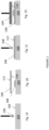
Figure 1 illustrates steps for forming an arrangement of a solder preform between a substrate and a semiconductor die, according to an embodiment. -
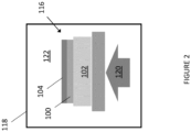
Figure 2 illustrates a soldering furnace that contains an arrangement of the solder preform between a substrate and a semiconductor die, according to an embodiment. -
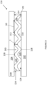
Figure 3 illustrates a side-view of an arrangement of a solder preform between a substrate and a semiconductor die wherein the solder preform has a varying surface profile, according to an embodiment. -
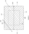
Figure 4 illustrates a plan-view of a solder preform with a varying surface profile, according to an embodiment. -
Figure 5 , which includesFigs. 5A-5C , illustrates side-views of solder preforms with a varying surface profile, according to various embodiments. - A mechanical pressure-free diffusion soldering technique that utilizes an advantageously configured solder preform is described herein. The solder preform comprises a varying surface profile on one or both surfaces of the solder preform that interface with the metal joining surfaces in the soldered joint. The varying surface profile has a non-planar geometry that creates voids between the solder preform and the semiconductor die and/or between the solder preform and the substrate before the solder is melted. These voids form channels that permit outgassing during pre-soldering steps that are performed on the assembly before the solder preform is melted. These pre-soldering steps may include an initial step that removes a tacking agent from the assembly and a subsequent step that de-oxidizes the soldering surfaces of the assembly. As a result, there is improved wetting between the solder preform and the semiconductor die and/or between the solder preform and the substrate, and hence improved quality of the completed soldered joint.
- Referring to
Figure 1 , selected steps for arranging a solder preform 100 in between asubstrate 102 and asemiconductor die 104 are depicted. While the figure depicts an arrangement with asingle semiconductor die 104, the techniques described herein are more generally applicable to batch soldering techniques wherein multiple semiconductor dies 104 are soldered at the same time. According to these batch soldering techniques, more than onesemiconductor die 104 can be soldered to the same ordifferent substrate 102 according to the same process. These semiconductor dies 104 may be the same or different from one another. - Referring to
Fig. 1A , asubstrate 102 comprising a firstmetal joining surface 106 is provided. Thesubstrate 102 is a carrier that is configured to accommodate the mounting of semiconductor dies 104 and/or passive electrical elements thereon. For example, thesubstrate 102 can be a PCB (printed circuit board) or apower electronics substrate 102 such as a DBC (direct bonded copper) substrate, an AMB (active metal brazed) substrate, or an insulated metal substrate (IMS). In these examples, thesubstrate 102 may comprise one or more dielectric layers (not shown) that are formed from ceramics (Al2O3, AlN, etc.), plastics, laminates, pre-peg materials (FR-2, FR-4, CEM-1, G-10, etc.), and a structured metallization layer disposed on an upper surface of thesubstrate 102, wherein the firstmetal joining surface 106 corresponds to a die attach surface of this structured metallization layer. Alternatively, thesubstrate 102 can be an exclusively metal structure, such as a lead frame. The firstmetal joining surface 106 can be provided by a metal structure that comprises or is plated with any or more of Cu, Ni, Ag, Au, Pd, Pt, NiV, NiP, NiNiP, NiP/Pd, Ni/Au, NiP/Pd/Au, or NiP/Pd/AuAg. In an embodiment, the firstmetal joining surface 106 is a bond pad or die pad that is formed from Cu or Cu alloy and has an Ni based coating formed on the outer surfaces of the Cu or Cu alloy. - A
tacking agent 108 is applied to the firstmetal joining surface 106. The tackingagent 108 is an inert substance that is used to keep the assembly of thesolder preform 100 and semiconductor die 104 in place during transportation to a solder furnace. Generally speaking, the tackingagent 108 can be any non-volatile, non-reactive liquid which keeps thesolder preform 100 in place on thesubstrate 102 by surface tension. For example, the tackingagent 108 can be a commercially available non-reactive liquid such as Fluorinert® Electronic Liquid FC-43, which is produced by 3M®. - Referring to
Fig. 1B , asolder preform 100 that comprises afirst interface surface 110 and asecond interface surface 112 opposite thefirst interface surface 110 is provided. Thesolder preform 100 may comprise Sn, Zn, In, Ga, Bi, Cd or any alloy thereof. For example, thesolder preform 100 may comprise Sn/Ag/Cu, Sn/Ag, Sn/Ag/Sb, Sn/Sb, Sn/Cu or Au80/Sn20. Still other types ofthin solder preforms 100 may be used. - Referring to
Fig. 1C , after thesolder preform 100 is arranged on thesubstrate 102, the tackingagent 108 is additionally applied to thesecond interface surface 112 of thesolder preform 100. The tackingagent 108 used in this step may be the same or different as the tackingagent 108 used to secure thesolder preform 100 to thesubstrate 102. - Referring to
Fig. 1D , asemiconductor die 104 is provided. The semiconductor die 104 comprises a secondmetal joining surface 114 that will be soldered to thesubstrate 102. The secondmetal joining surface 114 may be a bond pad of the semiconductor die 104. This bond pad may comprise and/or be plated with Cu, Ni, Ag, Au, Pd, Pt, NiV, NiP, NiNiP, NiP/Pd, Ni/Au, NiP/Pd/Au, NiP/Pd/AuAg, NiV/Ag, NiV/Au, or NiSi/Ag. Generally speaking, the semiconductor die 104 can have any device configuration. In an embodiment, the semiconductor die 104 is configured as a power transistor such as a MOSFET (metal-oxide semiconductor field-effect transistor), IGBT (insulated gate bipolar transistor), HEMT (high electron mobility transistor), etc. Alternatively, the semiconductor die 104 may be configured as a logic die such as a gate driver, microcontroller, memory, etc., or a passive die such as an inductor or capacitor die, etc. In these examples, the secondmetal joining surface 114 can be a bond pad that provides external accessibility to a device terminal, e.g., source, drain, collector, emitter, gate, anode, etc. - The semiconductor die 104 is arranged on the
solder preform 100 such that the secondmetal joining surface 114 faces thesolder preform 100 with the tackingagent 108 disposed between the two. The tackingagent 108 maintains the position of the semiconductor die 104 relative to thesolder preform 100 by surface tension. A clamping mechanism (not shown) may be used to handle thesolder preform 100 and to transport the assembly to a diffusion soldering oven. - As a result of the steps shown in
Figure 1 , thesolder preform 100 is arranged in between thesubstrate 102 and the semiconductor die 104 such that thefirst interface surface 110 faces the firstmetal joining surface 106 and such that thesecond interface surface 112 faces the secondmetal joining surface 114. Alternate methods may be used to obtain the same arrangement. For example, in another embodiment, thesolder preform 100 is initially applied to the semiconductor die 104. In this case, thesubstrate 102 inFig. 1B instead would be the semiconductor die 104 or a semiconductor wafer from which the die is produced. For example, thesolder preform 100 may be applied to a front side or a back side of a semiconductor wafer which includes the semiconductor die 104 and a plurality of additional semiconductor dies 104, or may be applied to the front side or back side of the semiconductor die 104 after the die singulation process. Subsequently, the semiconductor die 104 with thesolder preform 100 may be placed on the firstmetal joining surface 106 of thesubstrate 102 with a tackingagent 108 in between. - Referring to
Fig. 2 , thearrangement 116 of thesolder preform 100 between thesubstrate 102 and the semiconductor die 104 as described with reference toFig. 1 is placed in asoldering furnace 118. Thesoldering furnace 118 may be a vacuum oven that is configured to applyheat 120 to the assembly and to simultaneously vary the pressure within thesoldering furnace 118, including to vacuum conditions. - With the
arrangement 116 contained within the in thesoldering furnace 118, a mechanical pressure-free diffusion soldering process that forms a soldered joint between thesubstrate 102 and the semiconductor die 104 can be performed. According to this technique,heat 120 is applied to thearrangement 116 such that thesolder preform 100 melts and reacts with the first and secondmetal joining surfaces metal joining surface 106 comprises a different metal/metal alloy as the secondmetal joining surface 114, a plurality of different intermetallic phases are formed throughout the soldered joint. The intermetallic phases have a higher melting point than the soft solder alloy which forms which form the intermetallic phases, e.g., SnCu or SnSb2 in the above example. The presence of the intermetallic phases in the soldered joint results in the soldered joint having a high tensile strength that is durable with respect to thermal expansion forces caused by high temperature operation. The conditions of the soldering process (e.g., time and temperature) can be selected such that a significant percentage of the soldered joint consists of the intermetallic phases, e.g., intermetallic phase ratios of greater than 50%, greater than 75%, etc. Additionally or alternatively, the conditions of the soldering process can be selected such that the intermetallic phases are present throughout an entire thickness of the soldered joint. - The diffusion soldering process is a mechanical pressure-free diffusion soldering process. This means that no mechanical pressure is applied directly to the semiconductor die 104, e.g., from a movable press, during the melting and reaction of the solder material and/or during a subsequent hardening phase. In order to produce a soldered joint with desirable intermetallic phase characteristics, e.g., the intermetallic phase ratio and/or distribution of the intermetallic phases as described above, a
solder preform 100 that is relatively thin can be used, e.g., a thickness of no more than 50 µm, and more typically less than 30 µm. - The mechanical pressure-free diffusion soldering process may comprise performing one or more pre-soldering steps in the
soldering furnace 118 before the reflow (melting) of thesolder preform 100. During these pre-soldering steps, the temperature of thesoldering furnace 118 is maintained below a reflow temperature of thesolder preform 100. For example, a temperature in thesoldering furnace 118 may not exceed 200°C during the one or more pre-soldering steps. The pre-soldering steps may be performed to decontaminate thesoldering furnace 118 and/or to prepare thearrangement 116 of thesolder preform 100 in between thesubstrate 102 and the semiconductor die 104 for enhanced wettability of the solder material. - According to an embodiment, the pre-soldering steps comprise a conditioning step. The conditioning step conditions the chamber of the
soldering furnace 118 by removing contaminants. Additionally, the conditioning step evaporates the tackingagent 108 that was used to maintain the position of the semiconductor die 104 relative and thesolder preform 100 during the previous assembly steps. The conditioning step may include gradually ramping up the temperature in thesoldering furnace 118 from room temperature to an ending temperature of 100°C to 150°C. The conditioning step may include cycling the pressure in the chamber between high pressure conditions and vacuum conditions. A duration of the conditioning step may be between 300 and 500 seconds. - According to an embodiment, the pre-soldering steps comprise an activation step. The activation step removes oxide from the
solder preform 100 and the first and secondmetal joining surfaces soldering furnace 118, such that theambient atmosphere 122 of thesoldering furnace 118 comprises gaseous form of the deoxidizing agent. The activation step may be performed immediately after the conditioning step. During the activation step, the temperature of thesoldering furnace 118 may be gradually increased from the temperature of the conditioning step while still being below the reflow temperature of thesolder preform 100. For example, the activation step may begin at a temperature of about 100°C to 150°C and end at a temperature of no greater than 180°C to 190°C. A duration of the activation step may be between 420 and 540 seconds. - After performing the pre-soldering steps, the temperature of the
soldering furnace 118 is increased to create a reaction in thesolder preform 100 and create a soldered joint. During an initial melting phase, the temperature of thesoldering furnace 118 is increased to reach a melting temperature of thesolder preform 100. This initial melting phase may begin at a temperature of about 180°C to 190°C and end at a temperature of about 220°C to 230°C. A duration of the initial melting phase may be between about 240 and 360 seconds. Subsequently, the temperature of thesoldering furnace 118 may be increased such that thesolder preform 100 reacts with the first and secondmetal joining surfaces soldering furnace 118 may be increased. For example, the intermetallic phase formation step begin at a temperature of between 220°C to 230°C and end at a temperature of between 310°C to 330°C. A duration of the intermetallic phase formation step may be between 120 and 240 seconds. Finally, the temperature of thesoldering furnace 118 may be gradually reduced during a cooling phase such that the soldered joint between the semiconductor die 104 and thesubstrate 102 cools and hardens. - Referring to
Figure 3 , a close-up side view of thearrangement 116 of thesolder preform 100 in between thesubstrate 102 and the semiconductor die 104 before melting of thesolder preform 100 is depicted, according to an embodiment. In this embodiment, thesolder preform 100 is configured such that thefirst interface surface 110 and thesecond interface surface 112 each have a varyingsurface profile 124. A varyingsurface profile 124 refers to a surface that is non-planar. This non-planarity of the interfacing surfaces of thesolder preform 100 createsvoids 126 between thesolder preform 100 and thesubstrate 102 and createsvoids 126 between thesolder preform 100 and the semiconductor die 104. As a result, the ambient atmosphere 122 (or vacuum) contained within the chamber of thesoldering furnace 118 can extend into thearrangement 116 directly underneath the semiconductor die 104 and thesubstrate 102. - The
solder preform 100 with the varyingsurface profile 124 enhances the mechanical pressure-free diffusion soldering process in the following way. Thevoids 126 between thesolder preform 100 and thesubstrate 102 and/or between thesolder preform 100 and the semiconductor die 104 can be configured aschannels 130 that permit ingress and egress of theambient atmosphere 122 within thesoldering furnace 118. This improves the efficacy of the pre-soldering steps by facilitating the outgassing of thearrangement 116. In particular, during the conditioning step, vapours of the tackingagent 108 are outgassed through thesechannels 130. Additionally or alternatively, during the activation step, the formic acid can flow into thearrangement 116 via thechannels 130 and the consequent reacted oxide can exit thearrangement 116 via thechannels 130. - By way of comparison, a
solder preform 100 which has planar surfaces that interface with the semiconductor die 104 and/orsubstrate 102 is much more prohibitive of the pre-soldering steps. This is especially true at low thickness values for thesolder preform 100, e.g., less than 30µm, less than 15 µm, etc. These low thickness values, while preferable for forming a soldered joint with advantageous intermetallic phase characteristics, tend to cause thesolder preform 100 to conform to the surface profile of the semiconductor die 104 and/orsubstrate 102. This creates a sealing effect that prohibits removal of the tackingagent 108 and/or introduction of the deoxidizing agent. By contrast, the varyingsurface profile 124 of thesolder preform 100 described herein is intentionally formed to have sufficiently course texture to prevent thesolder preform 100 from settling into the metal surfaces to which it interfaces with. - The varying
surface profile 124 results from a textured profile that includes a plurality ofridges 128 andcorresponding channels 130 disposed between immediately adjacent ones of theridges 128. Theridges 128 refer to the highest point (i.e., the apex of the surface) and thechannels 130 refer to the surface between two immediatelyadjacent ridges 128. - According to an embodiment, the
solder preform 100 having the varyingsurface profile 124 has a thickness (T) of between 5 µm and 15 µm. The thickness (T) of thesolder preform 100 refers to a maximum separation distance between thefirst interface surface 110 and thesecond interface surface 112 in a direction that is orthogonal to these surfaces. This thickness (T) value produces a soldered joint by a mechanical pressure-free diffusion soldering with advantageous intermetallic phase characteristics. In the depicted embodiment, both of thefirst interface surface 110 and thesecond interface surface 112 have the same undulating profile such that thesolder preform 100 has a substantially uniform thickness (T) along a cross-section of thesolder preform 100 that is orthogonal to theridges 128 and thechannels 130. This thickness (T) may be a single thickness (T) in the range between 5 µm and 15 µm. This is not necessary, however. More generally, the profile of thefirst interface surface 110 and thesecond interface surface 112 may deviate from one another, and specific examples of such structures will be described in further detail below. In that case, the thickness (T) of thesolder preform 100 may vary across a particular cross-section in the range between 5 µm and 15 µm. - According to an embodiment, the
solder preform 100 having the varyingsurface profile 124 is configured such that a separation distance (SD) between two immediately adjacent ones of theridges 128 is between two and fifty times the thickness (T) of thesolder preform 100. Stated in numerical terms, the separation distance (SD) between two immediately adjacent ones of theridges 128 may be between 10 µm and 750 µm, for example. This separation distance (SD) may be sufficient to producevoids 126 that are effective and/or to prevent thesolder preform 100 from settling in the manner described above. - In the depicted embodiment, the varying
surface profile 124 is such that a plurality of theridges 128 are regularly spaced apart from one another by a fixed separation distance (SD). That is, along a cross-section of thesolder preform 100 that is orthogonal to theridges 128, the apex points occur at a constant wavelength. In that case, the fixed separation distance (SD) can be any value that is between two and fifty times the thickness (T) of thesolder preform 100. Thisarrangement 116 is not necessary, however. In other embodiments, the separation distance (SD) between any two immediately adjacent ones of theridges 128 may deviate from one another by any value that falls within the range of between two and fifty times the thickness (T) of thesolder preform 100. - According to an embodiment, a maximum vertical displacement (VD) of the
solder preform 100 between thefirst interface surface 110 and thesecond interface surface 112 is between four times the thickness (T) of thesolder preform 100 and ten times the thickness (T) of thesolder preform 100. The maximum vertical displacement (VD) refers to the largest distance between contact surfaces on opposite sides of thesolder preform 100 that are not necessarily laterally aligned with one another. In the depicted embodiment, the maximum vertical displacement (VD) is distance between an apex point on thefirst interface surface 110 and an apex point on thesecond interface surface 112. Stated in numerical terms, the maximum vertical displacement (VD) may be between 20 µm and 150 µm, for example. This maximum vertical displacement (VD) may be sufficient to producevoids 126 that are effective and/or to prevent thesolder preform 100 from settling in the manner described above. - Referring to
Figure 4 , a planar view of thesolder preform 100 is shown, according to an embodiment. The planar view may be above either one of thefirst interface surface 110 or thesecond interface surface 112. As can be seen, thesolder preform 100 is patterned such that theridges 128 run substantially parallel to one another in a lateral direction across thefirst interface surface 110 or thesecond interface surface 112. Correspondingly, thechannels 130 in between theridges 128 run substantially parallel to one another in a lateral direction across thefirst interface surface 110 or thesecond interface surface 112. While theridges 128 andcorresponding channels 130 in the depicted embodiment run along a single plane, this is not necessary. For example, theridges 128 andcorresponding channels 130 may have a wavy pattern. - According to an embodiment, at least one of the
channels 130 laterally extends completely between twoedge sides 132 of thesolder preform 100. With this configuration, at least one of thechannels 130 provides a complete passage for theambient atmosphere 122 in thesoldering furnace 118 to flow between twoedge sides 132 of thesolder preform 100. As a result, there can be an unimpeded flow of gas through thearrangement 116, which enhances the efficacy of the pre-soldering steps described above. As shown, the varyingsurface profile 124 has a diagonal pattern such that thechannels 130 extend between two orthogonal edge sides 132. More generally, the pattern of theridges 128 can be in any orientation. - According to an embodiment, at least one of the
channels 130 laterally extends from one edge side of thesolder preform 100 to acentral region 134 of thesolder preform 100. Thecentral region 134 is spaced apart from everyedge side 132 of thesolder preform 100. According to an embodiment, a distance between thecentral region 134 and the everyedge side 132 is between about 1-3 mm (millimetres). In one particular embodiment, thecentral region 134 is spaced apart from everyedge side 132 of thesolder preform 100 by 2 mm at every edge side. In general percentage terms, the distance between thecentral region 134 and the everyedge side 132 can be in the range of 10% to 50% of an overall width of the solder preform. Thecentral region 134 is a region is ordinarily sealed off from theambient atmosphere 122 in the case of asolder preform 100 that does not comprise the varyingsurface profile 124 as described herein. Thus, by configuring thesolder preform 100 such that thechannels 130 extend into thiscentral region 134, the efficacy of the pre-soldering steps described above is enhanced because the tackingagent 108 can be more effectively removed from thecentral region 134 and because portions of the first and secondmetal joining surfaces central region 134 can be more effectively deoxidized. - Referring to
Figure 5 , various embodiments of asolder preform 100 with a varyingsurface profile 124 are shown.Fig. 5A illustrates an example of asolder preform 100 wherein only one of the two interface surfaces has the varyingsurface profile 124. Hence, this type ofsolder preform 100 creates thevoids 126 between thesolder preform 100 and only one of thesubstrate 102 and the semiconductor die 104 before the melting of thesolder preform 100. For example, thesolder preform 100 ofFig. 5A may be arranged on thesubstrate 102 such that the rear planar surface corresponds to thefirst interface surface 110 and such that the varyingsurface profile 124 surface corresponds to thesecond interface surface 112. In that case, thevoids 126 form between the semiconductor die 104 and thesolder preform 100. Alternatively, thesolder preform 100 may be flipped upside down such that the varyingsurface profile 124 surface corresponds to thefirst interface surface 110 and the rear planar surface corresponds to thesecond interface surface 112. In that case, thevoids 126 form between thesubstrate 102 and thesolder preform 100. Thissolder preform 100 geometry may be preferable or acceptable if a particular metal surface is especially susceptible to oxidation with the other one being less-so.Fig. 5B illustrates an example of asolder preform 100 wherein the varyingsurface profile 124 has abrupt angled transitions instead of a gradually undulating, i.e., curved profile.Fig. 5C illustrates another example of asolder preform 100 with abrupt angled transitions, wherein the bottoms of thechannels 130 are widened to create a large volume. These two profiles may be preferred and/or acceptable alternatives, depending on the material and processes used to form the patterns. - More generally, the varying
surface profile 124 can have a wide variety of geometries different from the specific embodiments described herein while providing the advantageous ingress and egress of theambient atmosphere 122 during the pre-soldering steps as described above. For example, different radii, widths, angles, etc., may be provided in the varyingsurface profile 124 from what is shown. Additionally or alternatively, the first and second interfacing surfaces may differ from one another, and may have any of the varyingsurface profile 124 characteristics described herein. - A
solder preform 100 having the varyingsurface profile 124 may be formed according to the following technique. Initially, a preformed planar sheet of solder material having a thickness of, e.g., between 5 µm and 30 µm, may be provided. Subsequently, the preformed planar sheet of solder material is arranged between two pick and place tools and pressed together to obtain the desired surface profile. At least one of the two pick and place tools has a varying surface and imprints this into the solder to form the varyingsurface profile 124. In the case that the varyingsurface profile 124 is to be provided on both sides of thesolder preform 100, e.g., as shown inFig. 3 , two pick and place tools are pressed against opposite sides of the solder material, with the lower tool being the negative imprint of the upper tool. If the varyingsurface profile 124 is to be provided on only one side, e.g., as shown inFig. 5A , the upper one of the pick and place tools may have the desired imprint profile with the lower tool having a planar surface. The upper pick and place tool can be formed from a porous hard material, e.g., metal, and may include vacuum holes. The lower pick and place tool may be formed from a hard bulk material, e.g., metal, or a soft elastic material, e.g., rubber or plastic. - Terms such as "first", "second", and the like, are used to describe various elements, regions, sections, etc. and are also not intended to be limiting. Like terms refer to like elements throughout the description.
- As used herein, the terms "having", "containing", "including", "comprising" and the like are open ended terms that indicate the presence of stated elements or features, but do not preclude additional elements or features. The articles "a", "an" and "the" are intended to include the plural as well as the singular, unless the context clearly indicates otherwise.
- It is to be understood that the features of the various embodiments described herein may be combined with each other, unless specifically noted otherwise.
- Although specific embodiments have been illustrated and described herein, it will be appreciated by those of ordinary skill in the art that a variety of alternate and/or equivalent implementations may be substituted for the specific embodiments shown and described without departing from the scope of the present invention. This application is intended to cover any adaptations or variations of the specific embodiments discussed herein. Therefore, it is intended that this invention be limited only by the claims and the equivalents thereof.
Claims (14)
- A method of soldering a semiconductor device, the method comprising:providing a substrate comprising a first metal joining surface;providing a semiconductor die comprising a second metal joining surface;providing a solder preform that comprises a first interface surface and a second interface surface opposite the first interface surface;arranging the solder preform in between the substrate and the semiconductor die such that the first interface surface faces the first metal joining surface and such that the second interface surface faces the second metal joining surface; andperforming a mechanical pressure-free diffusion soldering process that forms a soldered joint between the substrate and the semiconductor die by melting the solder preform and forming intermetallic phases in the soldered joint;wherein one or both of the first interface surface and the second interface surface has a varying surface profile that creates voids between the solder preform and one or both of the substrate and the semiconductor die before the melting of the solder preform.
- The method of claim 1, wherein the varying surface profile comprises a plurality of ridges and channels that are disposed between immediately adjacent ones of the ridges, and wherein the channels create the voids in the arrangement of the solder preform in between the substrate and the semiconductor die.
- The method of claim 2, wherein at least one of the channels laterally extends completely between two edge sides of the solder preform.
- The method of claim 2, wherein at least one of the channels laterally extends from one edge side of the solder preform to a central region of the solder preform, wherein the central region is spaced apart from every edge side of the solder preform by at least 1 mm.
- The method of claim 2, wherein the ridges and channels have an undulating profile along a cross-section of the solder preform that is orthogonal to the ridges.
- The method of claim 5, wherein both of the first interface surface and the second interface surface have the same undulating profile, and wherein the solder preform has a substantially uniform thickness along the cross-section of the solder preform that is orthogonal to the ridges.
- The method of claim 2, wherein a thickness of the solder perform is between 5µm and 15 µm.
- The method of claim 7, wherein a separation distance between two immediately adjacent ones of the ridges is between two and fifty times the thickness of the solder preform.
- The method of claim 8, wherein the varying surface profile is such that a plurality of the ridges are regularly spaced apart from one another by a fixed separation distance that is between two and fifty times the thickness of the solder preform.
- The method of claim 7, wherein a maximum vertical displacement of the solder preform between the first interface surface and the second interface surface is between four times the thickness of the solder preform and ten times the thickness of the solder preform.
- The method of any of claims 1 - 10, wherein the solder preform comprises Sn, Zn, In, Ga, Bi, Cd or any alloy thereof.
- The method of any of claims 1 - 11, wherein performing the mechanical pressure-free diffusion soldering process comprises a conditioning step that removes a tacking agent from the arrangement of the solder preform in between the substrate and the semiconductor die.
- The method of any of claims 1 - 12, wherein performing the mechanical pressure-free diffusion soldering process comprises an activation step that introduces formic acid into a soldering furnace that contains the arrangement of the solder preform in between the substrate and the semiconductor die.
- A method of soldering a semiconductor device, the method comprising:providing a substrate comprising a first metal joining surface;providing a semiconductor die comprising a second metal joining surface;providing a solder preform that comprises a first interface surface and a second interface surface opposite the first interface surface;arranging the solder preform in between the substrate and the semiconductor die such that the first interface surface faces the first metal joining surface and such that the second interface surface faces the second metal joining surface;placing the arrangement of the solder preform in between the substrate and the semiconductor die in a soldering furnace;performing one or more pre-soldering steps in the soldering furnace below a reflow temperature of the solder preform with the arrangement of the solder preform contained in the soldering furnace;increasing the temperature of the soldering furnace to reach a melting temperature of the solder preform such that the solder preform melts and reacts with the first and second metal joining surfaces to form intermetallic phases in a soldered joint without applying mechanical pressure to the arrangement,wherein during the pre-soldering steps the arrangement of the solder preform in between the substrate and the semiconductor die comprises channels between the solder preform and one or both of the substrate and the semiconductor die, andwherein the channels permit ingress and egress of ambient atmosphere within the soldering furnace.
Applications Claiming Priority (1)
| Application Number | Priority Date | Filing Date | Title |
|---|---|---|---|
| US17/462,573 US11764185B2 (en) | 2021-08-31 | 2021-08-31 | Diffusion soldering preform with varying surface profile |
Publications (3)
| Publication Number | Publication Date |
|---|---|
| EP4141924A2 true EP4141924A2 (en) | 2023-03-01 |
| EP4141924A3 EP4141924A3 (en) | 2023-08-16 |
| EP4141924B1 EP4141924B1 (en) | 2024-07-24 |
Family
ID=83152108
Family Applications (1)
| Application Number | Title | Priority Date | Filing Date |
|---|---|---|---|
| EP22193090.2A Active EP4141924B1 (en) | 2021-08-31 | 2022-08-31 | Method of diffusion soldering a semiconductor device using a solder preform with varying surface profile |
Country Status (3)
| Country | Link |
|---|---|
| US (1) | US11764185B2 (en) |
| EP (1) | EP4141924B1 (en) |
| CN (1) | CN115722784A (en) |
Family Cites Families (12)
| Publication number | Priority date | Publication date | Assignee | Title |
|---|---|---|---|---|
| JPS6030102B2 (en) | 1980-07-14 | 1985-07-15 | ヤマハ株式会社 | Manufacturing method for semiconductor devices |
| US5616206A (en) * | 1993-06-15 | 1997-04-01 | Ricoh Company, Ltd. | Method for arranging conductive particles on electrodes of substrate |
| US7593228B2 (en) | 2005-10-26 | 2009-09-22 | Indium Corporation Of America | Technique for forming a thermally conductive interface with patterned metal foil |
| US20100247955A1 (en) * | 2006-09-29 | 2010-09-30 | Kabushiki Kaisha Toshiba | Joint with first and second members with a joining layer located therebetween containing sn metal and another metallic material; methods for forming the same |
| US20120255991A1 (en) | 2011-04-11 | 2012-10-11 | Andrew Llc | Corrugated Solder Pre-form and Method of Use |
| US9010616B2 (en) | 2011-05-31 | 2015-04-21 | Indium Corporation | Low void solder joint for multiple reflow applications |
| US9272371B2 (en) * | 2013-05-30 | 2016-03-01 | Agc Automotive Americas R&D, Inc. | Solder joint for an electrical conductor and a window pane including same |
| US9601451B2 (en) | 2015-08-11 | 2017-03-21 | Lenovo Enterprise Solutions (Singapore) Pte. Ltd. | Apparatus and methods for creating environmentally protective coating for integrated circuit assemblies |
| US11349274B2 (en) | 2018-10-16 | 2022-05-31 | Lumentum Operations Llc | Amplifier assembly |
| US11373976B2 (en) | 2019-08-02 | 2022-06-28 | Rockwell Collins, Inc. | System and method for extreme performance die attach |
| US11605608B2 (en) | 2019-11-11 | 2023-03-14 | Infineon Technologies Austria Ag | Preform diffusion soldering |
| US11158602B2 (en) | 2019-11-11 | 2021-10-26 | Infineon Technologies Austria Ag | Batch diffusion soldering and electronic devices produced by batch diffusion soldering |
-
2021
- 2021-08-31 US US17/462,573 patent/US11764185B2/en active Active
-
2022
- 2022-08-31 CN CN202211052969.4A patent/CN115722784A/en active Pending
- 2022-08-31 EP EP22193090.2A patent/EP4141924B1/en active Active
Also Published As
| Publication number | Publication date |
|---|---|
| US11764185B2 (en) | 2023-09-19 |
| CN115722784A (en) | 2023-03-03 |
| EP4141924B1 (en) | 2024-07-24 |
| US20230065738A1 (en) | 2023-03-02 |
| EP4141924A3 (en) | 2023-08-16 |
Similar Documents
| Publication | Publication Date | Title |
|---|---|---|
| US7560311B2 (en) | Robust leaded molded packages and methods for forming the same | |
| US9683278B2 (en) | Diffusion solder bonding using solder preforms | |
| JP2007268613A (en) | Diffusion soldering method | |
| EP4462478B1 (en) | Inkjet printing of diffusion solder | |
| US12394769B2 (en) | Batch soldering of different elements in power module | |
| EP3819058B1 (en) | Method of joining a semiconductor die to a substrate using preform diffusion soldering; corresponding semiconductor device | |
| EP4479998A2 (en) | Method of joining electrical and mechanical components using laminated modular preforms | |
| US9263299B2 (en) | Exposed die clip bond power package | |
| EP4141924B1 (en) | Method of diffusion soldering a semiconductor device using a solder preform with varying surface profile | |
| EP3819059B1 (en) | Method of batch diffusion soldering for soldering semiconductor dies to a substrate ; corresponding electronic device | |
| US11004823B2 (en) | Chip assembly and method of manufacturing thereof | |
| US20250349638A1 (en) | Electronic devices and methods of manufacturing electronic devices | |
| KR101726003B1 (en) | Substrate for power module, substrate for power module equiptted with heat sink, power module, and manufacturing method of substrate for power module | |
| Wu et al. | High temperature Ag-In joints between Si chips and aluminum | |
| CN121420693A (en) | Ceramic circuit board and its manufacturing method |
Legal Events
| Date | Code | Title | Description |
|---|---|---|---|
| PUAI | Public reference made under article 153(3) epc to a published international application that has entered the european phase |
Free format text: ORIGINAL CODE: 0009012 |
|
| STAA | Information on the status of an ep patent application or granted ep patent |
Free format text: STATUS: THE APPLICATION HAS BEEN PUBLISHED |
|
| AK | Designated contracting states |
Kind code of ref document: A2 Designated state(s): AL AT BE BG CH CY CZ DE DK EE ES FI FR GB GR HR HU IE IS IT LI LT LU LV MC MK MT NL NO PL PT RO RS SE SI SK SM TR |
|
| PUAL | Search report despatched |
Free format text: ORIGINAL CODE: 0009013 |
|
| AK | Designated contracting states |
Kind code of ref document: A3 Designated state(s): AL AT BE BG CH CY CZ DE DK EE ES FI FR GB GR HR HU IE IS IT LI LT LU LV MC MK MT NL NO PL PT RO RS SE SI SK SM TR |
|
| RIC1 | Information provided on ipc code assigned before grant |
Ipc: B23K 35/28 20060101ALI20230711BHEP Ipc: B23K 35/26 20060101ALI20230711BHEP Ipc: H01L 23/00 20060101ALI20230711BHEP Ipc: H01L 21/60 20060101ALI20230711BHEP Ipc: H01L 23/488 20060101AFI20230711BHEP |
|
| STAA | Information on the status of an ep patent application or granted ep patent |
Free format text: STATUS: REQUEST FOR EXAMINATION WAS MADE |
|
| 17P | Request for examination filed |
Effective date: 20231108 |
|
| RBV | Designated contracting states (corrected) |
Designated state(s): AL AT BE BG CH CY CZ DE DK EE ES FI FR GB GR HR HU IE IS IT LI LT LU LV MC MK MT NL NO PL PT RO RS SE SI SK SM TR |
|
| GRAP | Despatch of communication of intention to grant a patent |
Free format text: ORIGINAL CODE: EPIDOSNIGR1 |
|
| STAA | Information on the status of an ep patent application or granted ep patent |
Free format text: STATUS: GRANT OF PATENT IS INTENDED |
|
| RIC1 | Information provided on ipc code assigned before grant |
Ipc: B23K 35/28 20060101ALI20240314BHEP Ipc: B23K 35/26 20060101ALI20240314BHEP Ipc: H01L 23/00 20060101ALI20240314BHEP Ipc: H01L 21/60 20060101ALI20240314BHEP Ipc: H01L 23/488 20060101AFI20240314BHEP |
|
| INTG | Intention to grant announced |
Effective date: 20240412 |
|
| GRAS | Grant fee paid |
Free format text: ORIGINAL CODE: EPIDOSNIGR3 |
|
| GRAA | (expected) grant |
Free format text: ORIGINAL CODE: 0009210 |
|
| STAA | Information on the status of an ep patent application or granted ep patent |
Free format text: STATUS: THE PATENT HAS BEEN GRANTED |
|
| AK | Designated contracting states |
Kind code of ref document: B1 Designated state(s): AL AT BE BG CH CY CZ DE DK EE ES FI FR GB GR HR HU IE IS IT LI LT LU LV MC MK MT NL NO PL PT RO RS SE SI SK SM TR |
|
| REG | Reference to a national code |
Ref country code: GB Ref legal event code: FG4D |
|
| REG | Reference to a national code |
Ref country code: CH Ref legal event code: EP |
|
| P01 | Opt-out of the competence of the unified patent court (upc) registered |
Free format text: CASE NUMBER: APP_38573/2024 Effective date: 20240627 |
|
| REG | Reference to a national code |
Ref country code: IE Ref legal event code: FG4D Ref country code: DE Ref legal event code: R096 Ref document number: 602022004767 Country of ref document: DE |
|
| REG | Reference to a national code |
Ref country code: LT Ref legal event code: MG9D |
|
| REG | Reference to a national code |
Ref country code: NL Ref legal event code: MP Effective date: 20240724 |
|
| PG25 | Lapsed in a contracting state [announced via postgrant information from national office to epo] |
Ref country code: PT Free format text: LAPSE BECAUSE OF FAILURE TO SUBMIT A TRANSLATION OF THE DESCRIPTION OR TO PAY THE FEE WITHIN THE PRESCRIBED TIME-LIMIT Effective date: 20241125 |
|
| REG | Reference to a national code |
Ref country code: AT Ref legal event code: MK05 Ref document number: 1707144 Country of ref document: AT Kind code of ref document: T Effective date: 20240724 |
|
| PG25 | Lapsed in a contracting state [announced via postgrant information from national office to epo] |
Ref country code: NL Free format text: LAPSE BECAUSE OF FAILURE TO SUBMIT A TRANSLATION OF THE DESCRIPTION OR TO PAY THE FEE WITHIN THE PRESCRIBED TIME-LIMIT Effective date: 20240724 |
|
| PG25 | Lapsed in a contracting state [announced via postgrant information from national office to epo] |
Ref country code: PT Free format text: LAPSE BECAUSE OF FAILURE TO SUBMIT A TRANSLATION OF THE DESCRIPTION OR TO PAY THE FEE WITHIN THE PRESCRIBED TIME-LIMIT Effective date: 20241125 Ref country code: NL Free format text: LAPSE BECAUSE OF FAILURE TO SUBMIT A TRANSLATION OF THE DESCRIPTION OR TO PAY THE FEE WITHIN THE PRESCRIBED TIME-LIMIT Effective date: 20240724 |
|
| PG25 | Lapsed in a contracting state [announced via postgrant information from national office to epo] |
Ref country code: NO Free format text: LAPSE BECAUSE OF FAILURE TO SUBMIT A TRANSLATION OF THE DESCRIPTION OR TO PAY THE FEE WITHIN THE PRESCRIBED TIME-LIMIT Effective date: 20241024 |
|
| PG25 | Lapsed in a contracting state [announced via postgrant information from national office to epo] |
Ref country code: FI Free format text: LAPSE BECAUSE OF FAILURE TO SUBMIT A TRANSLATION OF THE DESCRIPTION OR TO PAY THE FEE WITHIN THE PRESCRIBED TIME-LIMIT Effective date: 20240724 Ref country code: PL Free format text: LAPSE BECAUSE OF FAILURE TO SUBMIT A TRANSLATION OF THE DESCRIPTION OR TO PAY THE FEE WITHIN THE PRESCRIBED TIME-LIMIT Effective date: 20240724 Ref country code: GR Free format text: LAPSE BECAUSE OF FAILURE TO SUBMIT A TRANSLATION OF THE DESCRIPTION OR TO PAY THE FEE WITHIN THE PRESCRIBED TIME-LIMIT Effective date: 20241025 |
|
| PG25 | Lapsed in a contracting state [announced via postgrant information from national office to epo] |
Ref country code: BG Free format text: LAPSE BECAUSE OF FAILURE TO SUBMIT A TRANSLATION OF THE DESCRIPTION OR TO PAY THE FEE WITHIN THE PRESCRIBED TIME-LIMIT Effective date: 20240724 |
|
| PG25 | Lapsed in a contracting state [announced via postgrant information from national office to epo] |
Ref country code: LV Free format text: LAPSE BECAUSE OF FAILURE TO SUBMIT A TRANSLATION OF THE DESCRIPTION OR TO PAY THE FEE WITHIN THE PRESCRIBED TIME-LIMIT Effective date: 20240724 |
|
| PG25 | Lapsed in a contracting state [announced via postgrant information from national office to epo] |
Ref country code: IS Free format text: LAPSE BECAUSE OF FAILURE TO SUBMIT A TRANSLATION OF THE DESCRIPTION OR TO PAY THE FEE WITHIN THE PRESCRIBED TIME-LIMIT Effective date: 20241124 Ref country code: AT Free format text: LAPSE BECAUSE OF FAILURE TO SUBMIT A TRANSLATION OF THE DESCRIPTION OR TO PAY THE FEE WITHIN THE PRESCRIBED TIME-LIMIT Effective date: 20240724 |
|
| PG25 | Lapsed in a contracting state [announced via postgrant information from national office to epo] |
Ref country code: HR Free format text: LAPSE BECAUSE OF FAILURE TO SUBMIT A TRANSLATION OF THE DESCRIPTION OR TO PAY THE FEE WITHIN THE PRESCRIBED TIME-LIMIT Effective date: 20240724 |
|
| PG25 | Lapsed in a contracting state [announced via postgrant information from national office to epo] |
Ref country code: ES Free format text: LAPSE BECAUSE OF FAILURE TO SUBMIT A TRANSLATION OF THE DESCRIPTION OR TO PAY THE FEE WITHIN THE PRESCRIBED TIME-LIMIT Effective date: 20240724 Ref country code: RS Free format text: LAPSE BECAUSE OF FAILURE TO SUBMIT A TRANSLATION OF THE DESCRIPTION OR TO PAY THE FEE WITHIN THE PRESCRIBED TIME-LIMIT Effective date: 20241024 |
|
| PG25 | Lapsed in a contracting state [announced via postgrant information from national office to epo] |
Ref country code: RS Free format text: LAPSE BECAUSE OF FAILURE TO SUBMIT A TRANSLATION OF THE DESCRIPTION OR TO PAY THE FEE WITHIN THE PRESCRIBED TIME-LIMIT Effective date: 20241024 Ref country code: PL Free format text: LAPSE BECAUSE OF FAILURE TO SUBMIT A TRANSLATION OF THE DESCRIPTION OR TO PAY THE FEE WITHIN THE PRESCRIBED TIME-LIMIT Effective date: 20240724 Ref country code: NO Free format text: LAPSE BECAUSE OF FAILURE TO SUBMIT A TRANSLATION OF THE DESCRIPTION OR TO PAY THE FEE WITHIN THE PRESCRIBED TIME-LIMIT Effective date: 20241024 Ref country code: LV Free format text: LAPSE BECAUSE OF FAILURE TO SUBMIT A TRANSLATION OF THE DESCRIPTION OR TO PAY THE FEE WITHIN THE PRESCRIBED TIME-LIMIT Effective date: 20240724 Ref country code: IS Free format text: LAPSE BECAUSE OF FAILURE TO SUBMIT A TRANSLATION OF THE DESCRIPTION OR TO PAY THE FEE WITHIN THE PRESCRIBED TIME-LIMIT Effective date: 20241124 Ref country code: HR Free format text: LAPSE BECAUSE OF FAILURE TO SUBMIT A TRANSLATION OF THE DESCRIPTION OR TO PAY THE FEE WITHIN THE PRESCRIBED TIME-LIMIT Effective date: 20240724 Ref country code: GR Free format text: LAPSE BECAUSE OF FAILURE TO SUBMIT A TRANSLATION OF THE DESCRIPTION OR TO PAY THE FEE WITHIN THE PRESCRIBED TIME-LIMIT Effective date: 20241025 Ref country code: FI Free format text: LAPSE BECAUSE OF FAILURE TO SUBMIT A TRANSLATION OF THE DESCRIPTION OR TO PAY THE FEE WITHIN THE PRESCRIBED TIME-LIMIT Effective date: 20240724 Ref country code: ES Free format text: LAPSE BECAUSE OF FAILURE TO SUBMIT A TRANSLATION OF THE DESCRIPTION OR TO PAY THE FEE WITHIN THE PRESCRIBED TIME-LIMIT Effective date: 20240724 Ref country code: BG Free format text: LAPSE BECAUSE OF FAILURE TO SUBMIT A TRANSLATION OF THE DESCRIPTION OR TO PAY THE FEE WITHIN THE PRESCRIBED TIME-LIMIT Effective date: 20240724 Ref country code: AT Free format text: LAPSE BECAUSE OF FAILURE TO SUBMIT A TRANSLATION OF THE DESCRIPTION OR TO PAY THE FEE WITHIN THE PRESCRIBED TIME-LIMIT Effective date: 20240724 |
|
| PG25 | Lapsed in a contracting state [announced via postgrant information from national office to epo] |
Ref country code: SM Free format text: LAPSE BECAUSE OF FAILURE TO SUBMIT A TRANSLATION OF THE DESCRIPTION OR TO PAY THE FEE WITHIN THE PRESCRIBED TIME-LIMIT Effective date: 20240724 Ref country code: DK Free format text: LAPSE BECAUSE OF FAILURE TO SUBMIT A TRANSLATION OF THE DESCRIPTION OR TO PAY THE FEE WITHIN THE PRESCRIBED TIME-LIMIT Effective date: 20240724 Ref country code: RO Free format text: LAPSE BECAUSE OF FAILURE TO SUBMIT A TRANSLATION OF THE DESCRIPTION OR TO PAY THE FEE WITHIN THE PRESCRIBED TIME-LIMIT Effective date: 20240724 |
|
| PG25 | Lapsed in a contracting state [announced via postgrant information from national office to epo] |
Ref country code: LU Free format text: LAPSE BECAUSE OF NON-PAYMENT OF DUE FEES Effective date: 20240831 |
|
| PG25 | Lapsed in a contracting state [announced via postgrant information from national office to epo] |
Ref country code: MC Free format text: LAPSE BECAUSE OF FAILURE TO SUBMIT A TRANSLATION OF THE DESCRIPTION OR TO PAY THE FEE WITHIN THE PRESCRIBED TIME-LIMIT Effective date: 20240724 Ref country code: EE Free format text: LAPSE BECAUSE OF FAILURE TO SUBMIT A TRANSLATION OF THE DESCRIPTION OR TO PAY THE FEE WITHIN THE PRESCRIBED TIME-LIMIT Effective date: 20240724 |
|
| PG25 | Lapsed in a contracting state [announced via postgrant information from national office to epo] |
Ref country code: CZ Free format text: LAPSE BECAUSE OF FAILURE TO SUBMIT A TRANSLATION OF THE DESCRIPTION OR TO PAY THE FEE WITHIN THE PRESCRIBED TIME-LIMIT Effective date: 20240724 |
|
| REG | Reference to a national code |
Ref country code: DE Ref legal event code: R097 Ref document number: 602022004767 Country of ref document: DE |
|
| PG25 | Lapsed in a contracting state [announced via postgrant information from national office to epo] |
Ref country code: SK Free format text: LAPSE BECAUSE OF FAILURE TO SUBMIT A TRANSLATION OF THE DESCRIPTION OR TO PAY THE FEE WITHIN THE PRESCRIBED TIME-LIMIT Effective date: 20240724 Ref country code: IT Free format text: LAPSE BECAUSE OF FAILURE TO SUBMIT A TRANSLATION OF THE DESCRIPTION OR TO PAY THE FEE WITHIN THE PRESCRIBED TIME-LIMIT Effective date: 20240724 |
|
| PLBE | No opposition filed within time limit |
Free format text: ORIGINAL CODE: 0009261 |
|
| STAA | Information on the status of an ep patent application or granted ep patent |
Free format text: STATUS: NO OPPOSITION FILED WITHIN TIME LIMIT |
|
| REG | Reference to a national code |
Ref country code: BE Ref legal event code: MM Effective date: 20240831 |
|
| 26N | No opposition filed |
Effective date: 20250425 |
|
| PG25 | Lapsed in a contracting state [announced via postgrant information from national office to epo] |
Ref country code: BE Free format text: LAPSE BECAUSE OF NON-PAYMENT OF DUE FEES Effective date: 20240831 |
|
| PG25 | Lapsed in a contracting state [announced via postgrant information from national office to epo] |
Ref country code: FR Free format text: LAPSE BECAUSE OF NON-PAYMENT OF DUE FEES Effective date: 20240924 |
|
| PG25 | Lapsed in a contracting state [announced via postgrant information from national office to epo] |
Ref country code: IE Free format text: LAPSE BECAUSE OF NON-PAYMENT OF DUE FEES Effective date: 20240831 |
|
| PG25 | Lapsed in a contracting state [announced via postgrant information from national office to epo] |
Ref country code: SE Free format text: LAPSE BECAUSE OF FAILURE TO SUBMIT A TRANSLATION OF THE DESCRIPTION OR TO PAY THE FEE WITHIN THE PRESCRIBED TIME-LIMIT Effective date: 20240724 |
|
| REG | Reference to a national code |
Ref country code: DE Ref legal event code: R079 Ref document number: 602022004767 Country of ref document: DE Free format text: PREVIOUS MAIN CLASS: H01L0023488000 Ipc: H10W0072000000 |
|
| PGFP | Annual fee paid to national office [announced via postgrant information from national office to epo] |
Ref country code: DE Payment date: 20251021 Year of fee payment: 4 |
|
| PG25 | Lapsed in a contracting state [announced via postgrant information from national office to epo] |
Ref country code: CY Free format text: LAPSE BECAUSE OF FAILURE TO SUBMIT A TRANSLATION OF THE DESCRIPTION OR TO PAY THE FEE WITHIN THE PRESCRIBED TIME-LIMIT; INVALID AB INITIO Effective date: 20220831 |
|
| PG25 | Lapsed in a contracting state [announced via postgrant information from national office to epo] |
Ref country code: HU Free format text: LAPSE BECAUSE OF FAILURE TO SUBMIT A TRANSLATION OF THE DESCRIPTION OR TO PAY THE FEE WITHIN THE PRESCRIBED TIME-LIMIT; INVALID AB INITIO Effective date: 20220831 |
|
| REG | Reference to a national code |
Ref country code: CH Ref legal event code: H13 Free format text: ST27 STATUS EVENT CODE: U-0-0-H10-H13 (AS PROVIDED BY THE NATIONAL OFFICE) Effective date: 20260324 |
|
| PG25 | Lapsed in a contracting state [announced via postgrant information from national office to epo] |
Ref country code: CH Free format text: LAPSE BECAUSE OF NON-PAYMENT OF DUE FEES Effective date: 20250831 |
|
| PG25 | Lapsed in a contracting state [announced via postgrant information from national office to epo] |
Ref country code: TR Free format text: LAPSE BECAUSE OF FAILURE TO SUBMIT A TRANSLATION OF THE DESCRIPTION OR TO PAY THE FEE WITHIN THE PRESCRIBED TIME-LIMIT Effective date: 20240724 |
|
| PG25 | Lapsed in a contracting state [announced via postgrant information from national office to epo] |
Ref country code: SI Free format text: LAPSE BECAUSE OF FAILURE TO SUBMIT A TRANSLATION OF THE DESCRIPTION OR TO PAY THE FEE WITHIN THE PRESCRIBED TIME-LIMIT Effective date: 20240724 |
|
| PG25 | Lapsed in a contracting state [announced via postgrant information from national office to epo] |
Ref country code: CH Free format text: THE PATENT HAS BEEN ANNULLED BY A DECISION OF A NATIONAL AUTHORITY Effective date: 20250831 |
|
| PG25 | Lapsed in a contracting state [announced via postgrant information from national office to epo] |
Ref country code: LT Free format text: LAPSE BECAUSE OF FAILURE TO SUBMIT A TRANSLATION OF THE DESCRIPTION OR TO PAY THE FEE WITHIN THE PRESCRIBED TIME-LIMIT Effective date: 20240724 |