EP4138141A1 - Semiconductor device, reservoir computing system, and method for manufacturing semiconductor device - Google Patents
Semiconductor device, reservoir computing system, and method for manufacturing semiconductor device Download PDFInfo
- Publication number
- EP4138141A1 EP4138141A1 EP20931249.5A EP20931249A EP4138141A1 EP 4138141 A1 EP4138141 A1 EP 4138141A1 EP 20931249 A EP20931249 A EP 20931249A EP 4138141 A1 EP4138141 A1 EP 4138141A1
- Authority
- EP
- European Patent Office
- Prior art keywords
- semiconductor region
- semiconductor
- insulating film
- semiconductor device
- nanowire
- Prior art date
- Legal status (The legal status is an assumption and is not a legal conclusion. Google has not performed a legal analysis and makes no representation as to the accuracy of the status listed.)
- Pending
Links
Images








Classifications
-
- H—ELECTRICITY
- H10—SEMICONDUCTOR DEVICES; ELECTRIC SOLID-STATE DEVICES NOT OTHERWISE PROVIDED FOR
- H10D—INORGANIC ELECTRIC SEMICONDUCTOR DEVICES
- H10D8/00—Diodes
- H10D8/70—Tunnel-effect diodes
-
- G—PHYSICS
- G06—COMPUTING OR CALCULATING; COUNTING
- G06N—COMPUTING ARRANGEMENTS BASED ON SPECIFIC COMPUTATIONAL MODELS
- G06N3/00—Computing arrangements based on biological models
- G06N3/02—Neural networks
- G06N3/04—Architecture, e.g. interconnection topology
- G06N3/044—Recurrent networks, e.g. Hopfield networks
-
- G—PHYSICS
- G06—COMPUTING OR CALCULATING; COUNTING
- G06N—COMPUTING ARRANGEMENTS BASED ON SPECIFIC COMPUTATIONAL MODELS
- G06N3/00—Computing arrangements based on biological models
- G06N3/02—Neural networks
- G06N3/06—Physical realisation, i.e. hardware implementation of neural networks, neurons or parts of neurons
- G06N3/063—Physical realisation, i.e. hardware implementation of neural networks, neurons or parts of neurons using electronic means
- G06N3/065—Analogue means
-
- H—ELECTRICITY
- H10—SEMICONDUCTOR DEVICES; ELECTRIC SOLID-STATE DEVICES NOT OTHERWISE PROVIDED FOR
- H10D—INORGANIC ELECTRIC SEMICONDUCTOR DEVICES
- H10D62/00—Semiconductor bodies, or regions thereof, of devices having potential barriers
- H10D62/10—Shapes, relative sizes or dispositions of the regions of the semiconductor bodies; Shapes of the semiconductor bodies
- H10D62/117—Shapes of semiconductor bodies
- H10D62/118—Nanostructure semiconductor bodies
- H10D62/119—Nanowire, nanosheet or nanotube semiconductor bodies
- H10D62/122—Nanowire, nanosheet or nanotube semiconductor bodies oriented at angles to substrates, e.g. perpendicular to substrates
-
- H—ELECTRICITY
- H10—SEMICONDUCTOR DEVICES; ELECTRIC SOLID-STATE DEVICES NOT OTHERWISE PROVIDED FOR
- H10D—INORGANIC ELECTRIC SEMICONDUCTOR DEVICES
- H10D62/00—Semiconductor bodies, or regions thereof, of devices having potential barriers
- H10D62/80—Semiconductor bodies, or regions thereof, of devices having potential barriers characterised by the materials
- H10D62/82—Heterojunctions
- H10D62/824—Heterojunctions comprising only Group III-V materials heterojunctions, e.g. GaN/AlGaN heterojunctions
-
- H—ELECTRICITY
- H10—SEMICONDUCTOR DEVICES; ELECTRIC SOLID-STATE DEVICES NOT OTHERWISE PROVIDED FOR
- H10D—INORGANIC ELECTRIC SEMICONDUCTOR DEVICES
- H10D64/00—Electrodes of devices having potential barriers
- H10D64/111—Field plates
-
- H—ELECTRICITY
- H10—SEMICONDUCTOR DEVICES; ELECTRIC SOLID-STATE DEVICES NOT OTHERWISE PROVIDED FOR
- H10D—INORGANIC ELECTRIC SEMICONDUCTOR DEVICES
- H10D8/00—Diodes
- H10D8/01—Manufacture or treatment
- H10D8/053—Manufacture or treatment of heterojunction diodes or of tunnel diodes
-
- H—ELECTRICITY
- H10—SEMICONDUCTOR DEVICES; ELECTRIC SOLID-STATE DEVICES NOT OTHERWISE PROVIDED FOR
- H10D—INORGANIC ELECTRIC SEMICONDUCTOR DEVICES
- H10D8/00—Diodes
- H10D8/70—Tunnel-effect diodes
- H10D8/75—Tunnel-effect PN diodes, e.g. Esaki diodes
-
- H—ELECTRICITY
- H10—SEMICONDUCTOR DEVICES; ELECTRIC SOLID-STATE DEVICES NOT OTHERWISE PROVIDED FOR
- H10D—INORGANIC ELECTRIC SEMICONDUCTOR DEVICES
- H10D84/00—Integrated devices formed in or on semiconductor substrates that comprise only semiconducting layers, e.g. on Si wafers or on GaAs-on-Si wafers
- H10D84/01—Manufacture or treatment
- H10D84/0112—Integrating together multiple components covered by H10D8/00, H10D10/00 or H10D18/00, e.g. integrating multiple BJTs
-
- H—ELECTRICITY
- H10—SEMICONDUCTOR DEVICES; ELECTRIC SOLID-STATE DEVICES NOT OTHERWISE PROVIDED FOR
- H10D—INORGANIC ELECTRIC SEMICONDUCTOR DEVICES
- H10D84/00—Integrated devices formed in or on semiconductor substrates that comprise only semiconducting layers, e.g. on Si wafers or on GaAs-on-Si wafers
- H10D84/01—Manufacture or treatment
- H10D84/02—Manufacture or treatment characterised by using material-based technologies
- H10D84/05—Manufacture or treatment characterised by using material-based technologies using Group III-V technology
-
- H—ELECTRICITY
- H10—SEMICONDUCTOR DEVICES; ELECTRIC SOLID-STATE DEVICES NOT OTHERWISE PROVIDED FOR
- H10D—INORGANIC ELECTRIC SEMICONDUCTOR DEVICES
- H10D84/00—Integrated devices formed in or on semiconductor substrates that comprise only semiconducting layers, e.g. on Si wafers or on GaAs-on-Si wafers
- H10D84/201—Integrated devices formed in or on semiconductor substrates that comprise only semiconducting layers, e.g. on Si wafers or on GaAs-on-Si wafers characterised by the integration of only components covered by H10D1/00 or H10D8/00, e.g. RLC circuits
- H10D84/204—Integrated devices formed in or on semiconductor substrates that comprise only semiconducting layers, e.g. on Si wafers or on GaAs-on-Si wafers characterised by the integration of only components covered by H10D1/00 or H10D8/00, e.g. RLC circuits of combinations of diodes or capacitors or resistors
- H10D84/221—Integrated devices formed in or on semiconductor substrates that comprise only semiconducting layers, e.g. on Si wafers or on GaAs-on-Si wafers characterised by the integration of only components covered by H10D1/00 or H10D8/00, e.g. RLC circuits of combinations of diodes or capacitors or resistors of only diodes
-
- H—ELECTRICITY
- H10—SEMICONDUCTOR DEVICES; ELECTRIC SOLID-STATE DEVICES NOT OTHERWISE PROVIDED FOR
- H10P—GENERIC PROCESSES OR APPARATUS FOR THE MANUFACTURE OR TREATMENT OF DEVICES COVERED BY CLASS H10
- H10P14/00—Formation of materials, e.g. in the shape of layers or pillars
- H10P14/20—Formation of materials, e.g. in the shape of layers or pillars of semiconductor materials
- H10P14/24—Formation of materials, e.g. in the shape of layers or pillars of semiconductor materials using chemical vapour deposition [CVD]
-
- H—ELECTRICITY
- H10—SEMICONDUCTOR DEVICES; ELECTRIC SOLID-STATE DEVICES NOT OTHERWISE PROVIDED FOR
- H10P—GENERIC PROCESSES OR APPARATUS FOR THE MANUFACTURE OR TREATMENT OF DEVICES COVERED BY CLASS H10
- H10P14/00—Formation of materials, e.g. in the shape of layers or pillars
- H10P14/20—Formation of materials, e.g. in the shape of layers or pillars of semiconductor materials
- H10P14/27—Formation of materials, e.g. in the shape of layers or pillars of semiconductor materials using selective deposition, e.g. simultaneous growth of monocrystalline and non-monocrystalline semiconductor materials
- H10P14/271—Formation of materials, e.g. in the shape of layers or pillars of semiconductor materials using selective deposition, e.g. simultaneous growth of monocrystalline and non-monocrystalline semiconductor materials characterised by the preparation of substrate for selective deposition
-
- H—ELECTRICITY
- H10—SEMICONDUCTOR DEVICES; ELECTRIC SOLID-STATE DEVICES NOT OTHERWISE PROVIDED FOR
- H10P—GENERIC PROCESSES OR APPARATUS FOR THE MANUFACTURE OR TREATMENT OF DEVICES COVERED BY CLASS H10
- H10P14/00—Formation of materials, e.g. in the shape of layers or pillars
- H10P14/20—Formation of materials, e.g. in the shape of layers or pillars of semiconductor materials
- H10P14/27—Formation of materials, e.g. in the shape of layers or pillars of semiconductor materials using selective deposition, e.g. simultaneous growth of monocrystalline and non-monocrystalline semiconductor materials
- H10P14/271—Formation of materials, e.g. in the shape of layers or pillars of semiconductor materials using selective deposition, e.g. simultaneous growth of monocrystalline and non-monocrystalline semiconductor materials characterised by the preparation of substrate for selective deposition
- H10P14/272—Formation of materials, e.g. in the shape of layers or pillars of semiconductor materials using selective deposition, e.g. simultaneous growth of monocrystalline and non-monocrystalline semiconductor materials characterised by the preparation of substrate for selective deposition using mask materials other than SiO2 or SiN
-
- H—ELECTRICITY
- H10—SEMICONDUCTOR DEVICES; ELECTRIC SOLID-STATE DEVICES NOT OTHERWISE PROVIDED FOR
- H10P—GENERIC PROCESSES OR APPARATUS FOR THE MANUFACTURE OR TREATMENT OF DEVICES COVERED BY CLASS H10
- H10P14/00—Formation of materials, e.g. in the shape of layers or pillars
- H10P14/20—Formation of materials, e.g. in the shape of layers or pillars of semiconductor materials
- H10P14/34—Deposited materials, e.g. layers
- H10P14/3402—Deposited materials, e.g. layers characterised by the chemical composition
- H10P14/3414—Deposited materials, e.g. layers characterised by the chemical composition being group IIIA-VIA materials
- H10P14/3421—Arsenides
-
- H—ELECTRICITY
- H10—SEMICONDUCTOR DEVICES; ELECTRIC SOLID-STATE DEVICES NOT OTHERWISE PROVIDED FOR
- H10P—GENERIC PROCESSES OR APPARATUS FOR THE MANUFACTURE OR TREATMENT OF DEVICES COVERED BY CLASS H10
- H10P14/00—Formation of materials, e.g. in the shape of layers or pillars
- H10P14/20—Formation of materials, e.g. in the shape of layers or pillars of semiconductor materials
- H10P14/34—Deposited materials, e.g. layers
- H10P14/3402—Deposited materials, e.g. layers characterised by the chemical composition
- H10P14/3414—Deposited materials, e.g. layers characterised by the chemical composition being group IIIA-VIA materials
- H10P14/3422—Antimonides
-
- H—ELECTRICITY
- H10—SEMICONDUCTOR DEVICES; ELECTRIC SOLID-STATE DEVICES NOT OTHERWISE PROVIDED FOR
- H10P—GENERIC PROCESSES OR APPARATUS FOR THE MANUFACTURE OR TREATMENT OF DEVICES COVERED BY CLASS H10
- H10P14/00—Formation of materials, e.g. in the shape of layers or pillars
- H10P14/20—Formation of materials, e.g. in the shape of layers or pillars of semiconductor materials
- H10P14/34—Deposited materials, e.g. layers
- H10P14/3438—Doping during depositing
- H10P14/3441—Conductivity type
- H10P14/3442—N-type
-
- H—ELECTRICITY
- H10—SEMICONDUCTOR DEVICES; ELECTRIC SOLID-STATE DEVICES NOT OTHERWISE PROVIDED FOR
- H10P—GENERIC PROCESSES OR APPARATUS FOR THE MANUFACTURE OR TREATMENT OF DEVICES COVERED BY CLASS H10
- H10P14/00—Formation of materials, e.g. in the shape of layers or pillars
- H10P14/20—Formation of materials, e.g. in the shape of layers or pillars of semiconductor materials
- H10P14/34—Deposited materials, e.g. layers
- H10P14/3438—Doping during depositing
- H10P14/3441—Conductivity type
- H10P14/3444—P-type
-
- H—ELECTRICITY
- H10—SEMICONDUCTOR DEVICES; ELECTRIC SOLID-STATE DEVICES NOT OTHERWISE PROVIDED FOR
- H10P—GENERIC PROCESSES OR APPARATUS FOR THE MANUFACTURE OR TREATMENT OF DEVICES COVERED BY CLASS H10
- H10P14/00—Formation of materials, e.g. in the shape of layers or pillars
- H10P14/20—Formation of materials, e.g. in the shape of layers or pillars of semiconductor materials
- H10P14/34—Deposited materials, e.g. layers
- H10P14/3451—Structure
- H10P14/3452—Microstructure
- H10P14/3462—Nanowires
Definitions
- the present disclosure relates to a semiconductor device, a reservoir computing system, and a method for manufacturing a semiconductor device.
- a network type circuit which includes a plurality of nonlinear elements having different nonlinear characteristics, is used.
- Non-Patent Document 1 Tsuyoshi Takahashi, Kenichi Kawaguchi, Masaru Sato, Michihiko Suhara, and Naoya Okamoto, "Realization of Large Breakdown Voltage of GaAsSb-Based Backward Diodes using Carrier Depletion Effect Originating from Nanowires", Extended Abstracts of the 2019 International Conference on Solid State Devices and Materials, Nagoya, 2019, pp195-196
- An object of the present disclosure is to provide a semiconductor device, a reservoir computing system, and a method for manufacturing a semiconductor device that are capable of arranging a plurality of nonlinear elements having different nonlinear characteristics with a high degree of integration.
- a semiconductor device including: a plurality of tunnel diodes, each of which includes a first semiconductor region of a first conductive type and a second semiconductor region of a second conductive type that is provided on the first semiconductor region and has a nanowire shape; an insulating film that covers a side surface of the second semiconductor region; a plurality of first electrodes, each connected to the first semiconductor region; and a plurality of second electrodes, each connected to the second semiconductor region, in which the second electrode has a first surface that faces the side surface of the second semiconductor region with the insulating film interposed therebetween, and diameters of the second semiconductor regions are different among the plurality of tunnel diodes.
- a semiconductor device includes a plurality of tunnel diodes, each of which includes a first semiconductor region of a first conductive type and a second semiconductor region of a second conductive type that is provided on the first semiconductor region and has a nanowire shape; an insulating film that covers a side surface of the second semiconductor region; a plurality of first electrodes, each connected to the first semiconductor region; and a plurality of second electrodes, each connected to the second semiconductor region, wherein the second electrode has a first surface that faces the side surface of the second semiconductor region with the insulating film interposed therebetween, and diameters of the second semiconductor regions are different among the plurality of tunnel diodes.
- a plurality of nonlinear elements having different nonlinear characteristics may be arranged with a high degree of integration.
- FIG. 1 is a cross-sectional view illustrating the semiconductor device according to the first embodiment.
- an n-type semiconductor layer 102 is formed on a substrate 101, and an insulating film 103 is formed on the n-type semiconductor layer 102.
- the insulating film 103 openings 21 and 22 reaching the n-type semiconductor layer 102 are formed.
- the substrate 101 is a semiinsulating (SI)-GaAs(111)B substrate
- the n-type semiconductor layer 102 is an n-type GaAs layer having a thickness of 100 nm to 300 nm.
- the insulating film 103 is a silicon nitride film having a thickness of 40 nm to 60 nm, and diameters of the openings 21 and 22 are 40 nm to 200 nm. The diameter of the opening 21 is larger than the diameter of the opening 22.
- the semiconductor device 100 includes a first nanowire 11 grown above the substrate 101 through the opening 21 and a second nanowire 12 grown above the substrate 101 through the opening 22.
- diameters of the first nanowire 11 and the second nanowire 12 are 40 nm to 200 nm.
- the first nanowire 11 is thicker than the second nanowire 12.
- the n-type semiconductor layer 102 is separated into a region connected to the first nanowire 11 and a region connected to the second nanowire 12 by an element separation groove 109.
- the first nanowire 11 has an n-type first semiconductor region 111 and a p-type second semiconductor region 112.
- the first semiconductor region 111 is provided on the n-type semiconductor layer 102 and extends upward.
- the second semiconductor region 112 is provided on the first semiconductor region 111 and extends upward.
- a metal film 31 is formed on the second semiconductor region 112.
- the metal film 31 is, for example, a gold (Au) film having a diameter of 40 nm to 200 nm.
- the second nanowire 12 has an n-type first semiconductor region 121 and a p-type second semiconductor region 122.
- the first semiconductor region 121 is provided on the n-type semiconductor layer 102 and extends upward.
- the second semiconductor region 122 is provided on the first semiconductor region 121 and extends upward.
- a metal film 32 is formed on the second semiconductor region 122.
- the metal film 32 is, for example, a gold (Au) film having a diameter of 40 nm to 200 nm.
- the second semiconductor regions 112 and 122 have a nanowire shape.
- the first semiconductor regions 111 and 121 may also have the nanowire shape.
- the first semiconductor regions 111 and 121 are n-type InAs nanowires
- the second semiconductor regions 112 and 122 are p-type GaAs 1-x Sb x nanowires.
- An Sb composition ratio x of GaAs 1-x Sb x is preferably 0.8 or more, and the Sb composition ratio x may be 1.0.
- the n-type first semiconductor region 111 and the p-type second semiconductor region 112 are in tunnel junction with each other, and the n-type first semiconductor region 121 and the p-type second semiconductor region 122 are in tunnel junction with each other.
- the first nanowire 11 and the second nanowire 12 are examples of tunnel diodes.
- Heights (lengths) of the first semiconductor regions 111 and 121 are, for example, 0.5 ⁇ m to 0.7 ⁇ m, and the height of the first semiconductor region 111 and the height of the first semiconductor region 121 may be equal to each other. Heights (lengths) of the second semiconductor regions 112 and 122 are, for example, 1.0 ⁇ m to 1.5 ⁇ m, and the height of the second semiconductor region 112 and the height of the second semiconductor region 122 may be equal to each other. Heights (lengths) of the first nanowire 11 and the second nanowire 12 are, for example, 1.5 ⁇ m to 2.0 ⁇ m, and the height of the first nanowire 11 and the height of the second nanowire 12 may be equal to each other.
- An insulating film 104 is formed to cover a side surface of the first nanowire 11 and a side surface of the second nanowire 12.
- the insulating film 104 is, for example, an aluminum oxide film or a hafnium oxide film having a thickness of 10 nm to 30 nm.
- the thickness referred to here is a thickness in a direction perpendicular to side surfaces 112A and 122A of the second semiconductor regions 112 and 122.
- the insulating film 104 is also formed on the insulating film 103.
- An organic insulating film 105 is formed on the insulating film 104.
- the organic insulating film 105 is, for example, a benzocyclobutene (BCB) film.
- An upper surface of the organic insulating film 105 is above a junction interface 113 between the first semiconductor region 111 and the second semiconductor region 112 and a junction interface 123 between the first semiconductor region 121 and the second semiconductor region 122.
- a metal film 41 in contact with the metal film 31 and a metal film 42 in contact with the metal film 32 are formed.
- the metal films 41 and 42 are, for example, laminated films of a platinum (Pt) film and a gold (Au) film thereon.
- the metal film 41 has a surface 41A facing the side surface 112A of the second semiconductor region 112 with the insulating film 104 interposed therebetween.
- the metal film 42 has a surface 42A facing the side surface 122A of the second semiconductor region 122 with the insulating film 104 interposed therebetween.
- a lower surface 41B of the metal film 41 and a lower surface 42B of the metal film 42 are above the junction interface 113 between the first semiconductor region 111 and the second semiconductor region 112 and the junction interface 123 between the first semiconductor region 121 and the second semiconductor region 122.
- the metal films 31 and 41 are included in an anode electrode 51, and the anode electrode 51 is in ohmic contact with the second semiconductor region 112.
- the metal films 32 and 42 are included in an anode electrode 52, and the anode electrode 52 is in ohmic contact with the second semiconductor region 122.
- the anode electrodes 51 and 52 are examples of second electrodes.
- the surfaces 41A and 42A are examples of first surfaces.
- an opening 71 reaching a region connected to the first semiconductor region 111 of the n-type semiconductor layer 102 and an opening 72 reaching a region connected to the first semiconductor region 121 of the n-type semiconductor layer 102 are formed.
- a cathode electrode 61 in contact with the n-type semiconductor layer 102 through the opening 71 and a cathode electrode 62 in contact with the n-type semiconductor layer 102 through the opening 72 are formed.
- the metal films 41 and 42 are, for example, laminated films of a gold germanium (AuGe) film and a gold (Au) film thereon.
- the cathode electrodes 61 and 62 are examples of first electrodes.
- FIG. 2 is a cross-sectional view illustrating the semiconductor device 100 according to the first embodiment during operation.
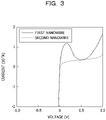
- FIG. 3 is a diagram illustrating voltage-current characteristics of the first nanowire 11 and the second nanowire 12.
- a depletion layer 114 is formed in the vicinity of the side surface 112A of the second semiconductor region 112 due to an influence of an electric field from the metal film 41.
- a depletion layer 124 is formed in the vicinity of the side surface 122A of the second semiconductor region 122 due to an influence of an electric field from the metal film 42.
- a diameter of the second semiconductor region 112 is larger a diameter of the second semiconductor region 122.
- a ratio of the depletion layer 114 occupying the second semiconductor region 112 in a radial direction is smaller than a ratio of the depletion layer 124 occupying the second semiconductor region 122 in the radial direction. Therefore, as illustrated in FIG. 3 , the voltage-current characteristic of the first nanowire 11 and the voltage-current characteristic of the second nanowire 12 are different. That is, nonlinear characteristics are different between the first nanowire 11 and the second nanowire 12.
- the first nanowire 11 functions as an Esaki diode and exhibits an S-shaped characteristic including a negative resistance component, while the second nanowire 12 exhibits a simple rectifying characteristic.
- the thickness of the insulating film 104 is preferably 10 nm or more and 30 nm or less, and more preferably 10 nm or more and 20 nm or less. In a case where the insulating film 104 is too thin, it may not be possible to sufficiently secure an insulating property between the second semiconductor region 112 and the metal film 41 and an insulating property between the second semiconductor region 122 and the metal film 42. In a case where the insulating film 104 is too thick, the depletion layers 114 and 124 may not be sufficiently formed.
- FIGs. 4 to 12 are cross-sectional views illustrating the method for manufacturing the semiconductor device 100 according to the first embodiment.
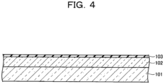
- the n-type semiconductor layer 102 is formed on the substrate 101.
- the n-type semiconductor layer 102 may be grown by, for example, a metal organic chemical vapor deposition (MOCVD) method.
- MOCVD metal organic chemical vapor deposition
- the insulating film 103 is formed on the n-type semiconductor layer 102.
- the openings 21 and 22 are formed in the insulating film 103.
- the openings 21 and 22 may be formed by, for example, forming a mask by lithography and etching the insulating film 103 by using the mask.
- the diameters of the openings 21 and 22 are assumed to be 40 nm to 200 nm, and the diameter of the opening 21 is made larger than the diameter of the opening 22.
- the disk-shaped metal film 31 is formed in the opening 21, and for example, the disk-shaped metal film 32 is formed in the opening 22.
- gold (Au) is used as a material of the metal films 31 and 32.
- a substrate for crystal growth including the substrate 101, the n-type semiconductor layer 102, the insulating film 103, the metal film 31, and the metal film 32 is obtained.
- the insulating film 103 in which the openings 21 and 22 are formed is an example of a growth mask.
- the first semiconductor regions 111 and 121 which include n-type GaAs and have a nanowire shape, are grown above the substrate 101.
- the first semiconductor region 111 is grown from the inside of the opening 21, and the first semiconductor region 121 is grown from the inside of the opening 22.
- the first semiconductor regions 111 and 121 may be grown by, for example, the MOCVD method.
- a growth temperature is 400°C to 450°C and the heights (lengths) of the first semiconductor regions 111 and 121 are 0.5 ⁇ m to 0.7 ⁇ m.
- TMGa triethylgallium
- AsH 3 arsine
- S hydrogen sulfide
- S sulfur
- a S concentration is, for example, 1 ⁇ 10 18 cm -3 to 1 ⁇ 10 20 cm -3 .
- Compositions of the first semiconductor regions 111 and 121 are equal to each other, and concentrations of the n-type impurities included in the first semiconductor regions 111 and 121 are also equal to each other.
- the second semiconductor regions 112 and 122 which include p-type GaAsSb and have a nanowire shape, are grown above the substrate 101.
- the second semiconductor region 112 is grown on the first semiconductor region 111
- the second semiconductor region 122 is grown on the first semiconductor region 121.
- the second semiconductor regions 112 and 122 may be grown by the MOCVD method in the same manner as the first semiconductor regions 111 and 121. For example, it is assumed that a growth temperature is 400°C to 450°C and the heights (lengths) of the second semiconductor regions 112 and 122 are 1.0 ⁇ m to 1.5 ⁇ m.
- triethylgallium (TEGa) is used as a raw material of Ga, arsine (AsH 3 ) is used as a raw material of As, and trimethylantimony (TMSb) is used as a raw material of Sb.
- arsine (AsH 3 ) is used as a raw material of As
- trimethylantimony (TMSb) is used as a raw material of Sb.
- diethylzinc (DEZn) is used as a raw material of a p-type impurity, and Zn is doped as the p-type impurity. It is assumed that a Zn concentration is, for example, 1 ⁇ 10 18 cm -3 to 1 ⁇ 10 20 cm -3 .
- Compositions of the second semiconductor regions 112 and 122 are equal to each other, and concentrations of the p-type impurities included in the second semiconductor regions 112 and 122 are also equal to each other.
- the first nanowire 11 including the first semiconductor region 111 and the second semiconductor region 112 and the second nanowire 12 including the first semiconductor region 121 and the second semiconductor region 122 are obtained.
- the diameter of the first nanowire 11 is larger than the diameter of the second nanowire 12.
- the insulating film 104 covering the first nanowire 11, the second nanowire 12, and the insulating film 103 is formed.
- the insulating film 104 for example, an aluminum oxide film or a hafnium oxide film having a thickness of 10 nm to 30 nm, preferably 10 nm to 20 nm is formed.
- the insulating film 104 may be formed by, for example, an atomic layer deposition (ALD) method.
- the element separation groove 109 is formed in the insulating film 104, the insulating film 103, and the n-type semiconductor layer 102.
- the element separation groove 109 is formed to separate the n-type semiconductor layer 102 into the region connected to the first nanowire 11 and the region connected to the second nanowire 12.
- the element separation groove 109 may be formed by, for example, forming a mask by lithography and etching the insulating film 104, the insulating film 103, and the n-type semiconductor layer 102 by using the mask.
- the organic insulating film 105 is formed on the insulating film 104 while filling the element separation groove 109.
- the organic insulating film 105 is preferably formed with a thickness such that the entire upper surface thereof is positioned above top portions of the metal films 31 and 32.
- a BCB film is formed as the organic insulating film 105.
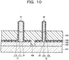
- the organic insulating film 105 is dry-etched until the upper surface thereof is thick enough to be positioned about 300 nm below top portions of the first nanowire 11 and the second nanowire 12.
- a mixed gas of carbon tetrafluoride (CF 4 ) and oxygen (O 2 ) may be used.
- Portions of the insulating film 104 covering the metal films 31 and 32 are also removed by using a difference in an etching rate between the organic insulating film 105 and the insulating film 104.
- the portions of the insulating film 104 covering the metal films 31 and 32 may be removed by, for example, ion sputtering using argon (Ar) ions after the dry etching of the organic insulating film 105.
- the metal film 41 in contact with the metal film 31 and the metal film 42 in contact with the metal film 32 are formed.
- the metal films 31 and 32 for example, laminated films of a platinum (Pt) film and a gold (Au) film thereon are formed.
- the metal films 31 and 41 are included in the anode electrode 51, and the metal films 32 and 42 are included in the anode electrode 52.
- the opening 71 reaching the region connected to the first semiconductor region 111 of the n-type semiconductor layer 102 and the opening 72 reaching the region connected to the first semiconductor region 121 of the n-type semiconductor layer 102 are formed.
- the openings 71 and 72 may be formed by, for example, forming a mask by lithography and etching the organic insulating film 105, the insulating film 104, and the insulating film 103 by using the mask.
- the insulating film 104 and the insulating film 103 may be removed by, for example, ion sputtering using argon (Ar) ions.
- Ar argon
- the cathode electrode 61 in contact with the n-type semiconductor layer 102 through the opening 71 and the cathode electrode 62 in contact with the n-type semiconductor layer 102 through the opening 72 are formed.
- the metal films 41 and 42 for example, laminated films of a gold germanium (AuGe) film and a gold (Au) film thereon are formed.
- the semiconductor device 100 according to the first embodiment may be manufactured.
- the semiconductor device 100 in which a plurality of nanowires (the first nanowire 11 and the second nanowire 12) having different voltage-current characteristics are arranged with a high degree of integration. Therefore, a plurality of nonlinear elements having different nonlinear characteristics may be arranged with a high degree of integration.
- first nanowire 11 and the second nanowire 12 are provided above the substrate 101, but a larger number of nanowires may be provided.
- the first semiconductor regions 111 and 121 need not have a nanowire shape, but the second semiconductor regions 112 and 122 having the nanowire shape are more easily formed when the first semiconductor regions 111 and 121 have the nanowire shape.
- FIG. 13 is a diagram illustrating voltage-current characteristics of nanowires with various second semiconductor regions with different diameters.
- the diameter region where a forward current transitions from the microampere order to the nanoampere order a forward tunnel current may be greatly changed, and various nonlinear elements may be prepared collectively. From this point of view, in the example illustrated in FIG. 13 , the diameter is preferably about 60 nm to 200 nm.
- FIG. 14 is a diagram illustrating voltage-current characteristics of nanowires with various second semiconductor regions of different doping concentrations.
- voltage-current characteristics of nanowires having a second semiconductor region with a diameter of 60 nm and a doping concentration ⁇ of 1 ⁇ 10 17 cm -3 to 5 ⁇ 10 18 cm -3 are illustrated.
- the doping concentration is preferably about 5 ⁇ 10 17 cm -3 to 5 ⁇ 10 18 cm -3 .
- the diameter d in Expression (1) is the diameter on the upper surface of the second semiconductor region.
- FIGs. 15 and 16 are diagrams illustrating the reservoir circuit according to the second embodiment.
- FIG. 15 is a circuit diagram illustrating a connection relationship of a plurality of nanowires
- FIG. 16 is a cross-sectional view illustrating the connection relationship of the plurality of nanowires.
- a part of configurations such as an insulating film are omitted.
- a reservoir circuit 200 includes a substrate 101, an n-type semiconductor layer 102, a plurality of nanowires 20, a wire 233, a wire 234, a wire 235, a wire 236, an input terminal 231, and an output terminal 232.
- the nanowire 20 has an n-type first semiconductor region 201 and a p-type second semiconductor region 202.
- the first semiconductor region 201 is provided on the n-type semiconductor layer 102 and extends upward.
- the second semiconductor region 202 is provided on the first semiconductor region 201 and extends upward. Diameters are different among the plurality of nanowires 20. Not all the nanowires 20 need to be different in diameter and nanowires 20 with equal diameter may be included.
- the n-type semiconductor layer 102 is element-separated for each nanowire 20.
- the plurality of nanowires 20 is arranged at equal intervals in two directions (X direction and Y direction) orthogonal to each other.
- the plurality of nanowires 20 is arranged in a grid pattern in a plan view above the substrate 101.
- the input terminal 231 and the output terminal 232 are provided in the same number as the number of rows including the plurality of nanowires 20 arranged in the X direction.
- the wire 233 connects the input terminal 231 and the second semiconductor region 202 of the nanowire 20 positioned at one end of the plurality of nanowires 20 arranged in the X direction.
- the wire 234 connects the output terminal 232 and the n-type semiconductor layer 102 connected to the first semiconductor region 201 of the nanowire 20 positioned at the other end of the plurality of nanowires 20 arranged in the X direction.
- the wire 235 connects the n-type semiconductor layer 102 connected to one first semiconductor region 201 and the other second semiconductor region 202 between two nanowires 20 adjacent to each other in the X direction.
- the wire 236 connects one second semiconductor region 202 and the other second semiconductor region 202 between two nanowires 20 adjacent to each other in the Y direction.
- a part of the wire 233 and a part of the wire 236 function as anode electrodes, and a part of the wire 234 functions as a cathode electrode.
- a part of the wire 235 functions as an anode electrode, and another part thereof functions as a cathode electrode.
- the portions of the wires 233, 235, and 236 that function as anode electrodes are configured to include surfaces that face side surfaces of the second semiconductor regions 202 with an insulating film 204 interposed therebetween.
- the plurality of nanowires 20 having different nonlinear characteristics is connected in a network shape. Therefore, the reservoir circuit 200 including a plurality of nonlinear elements having various nonlinear characteristics with a high degree of integration is obtained. Furthermore, since the nonlinear characteristics are different among the plurality of nanowires 20 when the diameters are different even when materials and compositions are the same, manufacturing may be performed without needing complicated processing.
- FIG. 17 is a diagram illustrating a reservoir circuit according to the modification of the second embodiment.
- FIG. 17 is a circuit diagram illustrating the connection relationship of the plurality of nanowires.
- the wire 235 is not provided in a part of pairs of nanowires 20 adjacent to each other in the X direction. Furthermore, the wire 236 is not provided in a part of pairs of nanowires 20 adjacent to each other in the Y direction.
- irregularity of the network of the nonlinear elements may be made higher than that of the reservoir circuit 200 according to the second embodiment.
- a plurality of the second semiconductor regions is connected or the first semiconductor region and the second semiconductor region are connected through the wire, but a plurality of the first semiconductor regions may be connected through the wire.
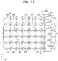
- FIG. 18 is a circuit diagram illustrating a connection relationship of a plurality of nanowires
- FIG. 19 is a cross-sectional view illustrating the connection relationship of the plurality of nanowires.
- a part of configurations such as an insulating film are omitted.
- a reservoir circuit 300 includes a substrate 101, an n-type semiconductor layer 102, a plurality of nanowires 20, a wire 233, a wire 234, a wire 235, a wire 236, a wire 237, a variable weighting circuit 238, an input terminal 231, and an output terminal 232.
- the substrate 101, the n-type semiconductor layer 102, the plurality of nanowires 20, the wire 233, the wire 235, and the wire 236 are configured similarly to those in the second embodiment.
- the variable weighting circuit 238 includes an oxide memristor 239 provided for each row including the plurality of nanowires 20 arranged in an X direction.
- the wire 234 connects one end of the oxide memristor 239 and the n-type semiconductor layer 102 connected to a first semiconductor region 201 of the nanowire 20 positioned at the other end of the plurality of nanowires 20 arranged in the X direction.
- the wire 237 connects the output terminal 232 and the n-type semiconductor layer 102 to which the other end of the oxide memristor 239 is connected.
- the oxide memristor 239 is an example of an analog memory.
- a resistance of the oxide memristor 239 changes according to a current (signal intensity) output from the plurality of nanowires 20 through the wire 234, and weight information is held in the variable weighting circuit 238.
- the reservoir circuit 300 according to the third embodiment corresponds to a device which integrates up to linear reading in a reservoir computing system.
- a fourth embodiment relates to a reservoir computing system including a reservoir circuit.
- FIG. 20 is a block diagram illustrating the reservoir computing system according to the fourth embodiment.
- a reservoir computing system 400 includes an input circuit 401, a reservoir circuit 402, and an output circuit 403.
- the reservoir circuit 402 includes a reading and weighting unit 404.
- the reservoir computing system 400 may further include a training data circuit 405.
- the reservoir circuit 402 the reservoir circuit 200 or 300 may be used.
- training data (teacher data) is input from the training data circuit 405 to the reading and weighting unit 404, and the reading and weighting unit 404 is adjusted so that appropriate weighting is performed.
- the reading and weighting unit 404 is an example of an analog memory.
- the training data circuit 405 is separated from the reservoir circuit 402. Then, data is input from the input circuit 401 to the reservoir circuit 402, and in the reservoir circuit 402, arithmetic processing such as weighting by the reading and weighting unit 404 is performed on the input data. A result of the arithmetic processing in the reservoir circuit 402 is output from the output circuit 403.
- nanowires which are a plurality of nonlinear elements included in the reservoir computing system 400, may be arranged with a high degree of integration.
Landscapes
- Engineering & Computer Science (AREA)
- Physics & Mathematics (AREA)
- Theoretical Computer Science (AREA)
- Biomedical Technology (AREA)
- Health & Medical Sciences (AREA)
- Life Sciences & Earth Sciences (AREA)
- Biophysics (AREA)
- General Health & Medical Sciences (AREA)
- Software Systems (AREA)
- Computational Linguistics (AREA)
- Data Mining & Analysis (AREA)
- Evolutionary Computation (AREA)
- Artificial Intelligence (AREA)
- Molecular Biology (AREA)
- Computing Systems (AREA)
- General Engineering & Computer Science (AREA)
- General Physics & Mathematics (AREA)
- Mathematical Physics (AREA)
- Neurology (AREA)
- Electrodes Of Semiconductors (AREA)
- Nanotechnology (AREA)
- Chemical & Material Sciences (AREA)
- Semiconductor Memories (AREA)
- Semiconductor Integrated Circuits (AREA)
Abstract
Description
- The present disclosure relates to a semiconductor device, a reservoir computing system, and a method for manufacturing a semiconductor device.
- In order to provide advanced information processing services using artificial intelligence, development of computing systems for the AI has been advanced. There is a growing movement to implement such systems by adopting neuromorphic computing inspired by a neural model of a living body. In the movement, reservoir computing is expected as a technology to advance AI, such as recognition and prediction of a moving image, because the reservoir computing is capable of time-series information processing. In a reservoir computing system, a network type circuit called a reservoir circuit, which includes a plurality of nonlinear elements having different nonlinear characteristics, is used.
-
- Patent Document 1:
Japanese Laid-open Patent Publication No. 8-213561 - Patent Document 2:
Japanese Laid-open Patent Publication No. 2011-238909 - Patent Document 3: Japanese National Publication of International Patent Application No.
2015-529006 - Non-Patent Document 1: Tsuyoshi Takahashi, Kenichi Kawaguchi, Masaru Sato, Michihiko Suhara, and Naoya Okamoto, "Realization of Large Breakdown Voltage of GaAsSb-Based Backward Diodes using Carrier Depletion Effect Originating from Nanowires", Extended Abstracts of the 2019 International Conference on Solid State Devices and Materials, Nagoya, 2019, pp195-196
- It is difficult to arrange a plurality of nonlinear elements having different nonlinear characteristics with a high degree of integration.
- An object of the present disclosure is to provide a semiconductor device, a reservoir computing system, and a method for manufacturing a semiconductor device that are capable of arranging a plurality of nonlinear elements having different nonlinear characteristics with a high degree of integration.
- According to one form of the present disclosure, there is provided a semiconductor device including: a plurality of tunnel diodes, each of which includes a first semiconductor region of a first conductive type and a second semiconductor region of a second conductive type that is provided on the first semiconductor region and has a nanowire shape; an insulating film that covers a side surface of the second semiconductor region; a plurality of first electrodes, each connected to the first semiconductor region; and a plurality of second electrodes, each connected to the second semiconductor region, in which the second electrode has a first surface that faces the side surface of the second semiconductor region with the insulating film interposed therebetween, and diameters of the second semiconductor regions are different among the plurality of tunnel diodes.
- According to an aspect of the embodiments, a semiconductor device includes a plurality of tunnel diodes, each of which includes a first semiconductor region of a first conductive type and a second semiconductor region of a second conductive type that is provided on the first semiconductor region and has a nanowire shape; an insulating film that covers a side surface of the second semiconductor region; a plurality of first electrodes, each connected to the first semiconductor region; and a plurality of second electrodes, each connected to the second semiconductor region, wherein the second electrode has a first surface that faces the side surface of the second semiconductor region with the insulating film interposed therebetween, and diameters of the second semiconductor regions are different among the plurality of tunnel diodes.
- According to the present disclosure, a plurality of nonlinear elements having different nonlinear characteristics may be arranged with a high degree of integration.
-
-
FIG. 1 is a cross-sectional view illustrating a semiconductor device according to a first embodiment; -
FIG. 2 is a cross-sectional view illustrating the semiconductor device according to the first embodiment during operation; -
FIG. 3 is a diagram illustrating voltage-current characteristics of nanowires; -
FIG. 4 is a cross-sectional view (part 1) illustrating a method for manufacturing the semiconductor device according to the first embodiment; -
FIG. 5 is a cross-sectional view (part 2) illustrating the method for manufacturing the semiconductor device according to the first embodiment; -
FIG. 6 is a cross-sectional view (part 3) illustrating the method for manufacturing the semiconductor device according to the first embodiment; -
FIG. 7 is a cross-sectional view (part 4) illustrating the method for manufacturing the semiconductor device according to the first embodiment; -
FIG. 8 is a cross-sectional view (part 5) illustrating the method for manufacturing the semiconductor device according to the first embodiment; -
FIG. 9 is a cross-sectional view (part 6) illustrating the method for manufacturing the semiconductor device according to the first embodiment; -
FIG. 10 is a cross-sectional view (part 7) illustrating the method for manufacturing the semiconductor device according to the first embodiment; -
FIG. 11 is a cross-sectional view (part 8) illustrating the method for manufacturing the semiconductor device according to the first embodiment; -
FIG. 12 is a cross-sectional view (part 9) illustrating the method for manufacturing the semiconductor device according to the first embodiment; -
FIG. 13 is a diagram illustrating voltage-current characteristics of nanowires with various second semiconductor regions with different diameters; -
FIG. 14 is a diagram illustrating voltage-current characteristics of nanowires with various second semiconductor regions of different doping concentrations; -
FIG. 15 is a circuit diagram illustrating a reservoir circuit according to a second embodiment; -
FIG. 16 is a cross-sectional view illustrating the reservoir circuit according to the second embodiment; -
FIG. 17 is a circuit diagram illustrating a reservoir circuit according to a modification of the second embodiment; -
FIG. 18 is a circuit diagram illustrating a reservoir circuit according to a third embodiment; -
FIG. 19 is a cross-sectional view illustrating the reservoir circuit according to the third embodiment; and -
FIG. 20 is a block diagram illustrating a reservoir computing system according to a fourth embodiment. - Hereinafter, embodiments of the present disclosure will be specifically described with reference to the accompanying drawings. Note that, in the present specification and drawings, components having substantially the same functional configuration are denoted by the same reference signs, and redundant description may be omitted.
- A first embodiment will be described. The first embodiment relates to a semiconductor device including a semiconductor region having a nanowire shape.
FIG. 1 is a cross-sectional view illustrating the semiconductor device according to the first embodiment. - As illustrated in
FIG. 1 , in asemiconductor device 100 according to the first embodiment, an n-type semiconductor layer 102 is formed on asubstrate 101, and aninsulating film 103 is formed on the n-type semiconductor layer 102. In theinsulating film 103,openings type semiconductor layer 102 are formed. For example, thesubstrate 101 is a semiinsulating (SI)-GaAs(111)B substrate, and the n-type semiconductor layer 102 is an n-type GaAs layer having a thickness of 100 nm to 300 nm. For example, theinsulating film 103 is a silicon nitride film having a thickness of 40 nm to 60 nm, and diameters of theopenings opening 21 is larger than the diameter of the opening 22. - The
semiconductor device 100 includes afirst nanowire 11 grown above thesubstrate 101 through the opening 21 and asecond nanowire 12 grown above thesubstrate 101 through the opening 22. For example, diameters of thefirst nanowire 11 and thesecond nanowire 12 are 40 nm to 200 nm. Thefirst nanowire 11 is thicker than thesecond nanowire 12. The n-type semiconductor layer 102 is separated into a region connected to thefirst nanowire 11 and a region connected to thesecond nanowire 12 by anelement separation groove 109. - The
first nanowire 11 has an n-typefirst semiconductor region 111 and a p-typesecond semiconductor region 112. Thefirst semiconductor region 111 is provided on the n-type semiconductor layer 102 and extends upward. Thesecond semiconductor region 112 is provided on thefirst semiconductor region 111 and extends upward. Ametal film 31 is formed on thesecond semiconductor region 112. Themetal film 31 is, for example, a gold (Au) film having a diameter of 40 nm to 200 nm. - The
second nanowire 12 has an n-typefirst semiconductor region 121 and a p-typesecond semiconductor region 122. Thefirst semiconductor region 121 is provided on the n-type semiconductor layer 102 and extends upward. Thesecond semiconductor region 122 is provided on thefirst semiconductor region 121 and extends upward. Ametal film 32 is formed on thesecond semiconductor region 122. Themetal film 32 is, for example, a gold (Au) film having a diameter of 40 nm to 200 nm. - The
second semiconductor regions first semiconductor regions first semiconductor regions second semiconductor regions first semiconductor region 111 and the p-typesecond semiconductor region 112 are in tunnel junction with each other, and the n-typefirst semiconductor region 121 and the p-typesecond semiconductor region 122 are in tunnel junction with each other. Thefirst nanowire 11 and thesecond nanowire 12 are examples of tunnel diodes. - Heights (lengths) of the
first semiconductor regions first semiconductor region 111 and the height of thefirst semiconductor region 121 may be equal to each other. Heights (lengths) of thesecond semiconductor regions second semiconductor region 112 and the height of thesecond semiconductor region 122 may be equal to each other. Heights (lengths) of thefirst nanowire 11 and thesecond nanowire 12 are, for example, 1.5 µm to 2.0 µm, and the height of thefirst nanowire 11 and the height of thesecond nanowire 12 may be equal to each other. - An insulating
film 104 is formed to cover a side surface of thefirst nanowire 11 and a side surface of thesecond nanowire 12. The insulatingfilm 104 is, for example, an aluminum oxide film or a hafnium oxide film having a thickness of 10 nm to 30 nm. The thickness referred to here is a thickness in a direction perpendicular toside surfaces second semiconductor regions film 104 is also formed on the insulatingfilm 103. - An organic insulating
film 105 is formed on the insulatingfilm 104. The organicinsulating film 105 is, for example, a benzocyclobutene (BCB) film. An upper surface of the organic insulatingfilm 105 is above ajunction interface 113 between thefirst semiconductor region 111 and thesecond semiconductor region 112 and ajunction interface 123 between thefirst semiconductor region 121 and thesecond semiconductor region 122. - On the organic insulating
film 105, ametal film 41 in contact with themetal film 31 and ametal film 42 in contact with themetal film 32 are formed. Themetal films metal film 41 has asurface 41A facing theside surface 112A of thesecond semiconductor region 112 with the insulatingfilm 104 interposed therebetween. Themetal film 42 has asurface 42A facing theside surface 122A of thesecond semiconductor region 122 with the insulatingfilm 104 interposed therebetween. For example, alower surface 41B of themetal film 41 and alower surface 42B of themetal film 42 are above thejunction interface 113 between thefirst semiconductor region 111 and thesecond semiconductor region 112 and thejunction interface 123 between thefirst semiconductor region 121 and thesecond semiconductor region 122. Themetal films anode electrode 51, and theanode electrode 51 is in ohmic contact with thesecond semiconductor region 112. Themetal films anode electrode 52, and theanode electrode 52 is in ohmic contact with thesecond semiconductor region 122. Theanode electrodes surfaces - In the organic insulating
film 105, the insulatingfilm 104, and the insulatingfilm 103, anopening 71 reaching a region connected to thefirst semiconductor region 111 of the n-type semiconductor layer 102 and anopening 72 reaching a region connected to thefirst semiconductor region 121 of the n-type semiconductor layer 102 are formed. On the organic insulatingfilm 105, acathode electrode 61 in contact with the n-type semiconductor layer 102 through theopening 71 and acathode electrode 62 in contact with the n-type semiconductor layer 102 through theopening 72 are formed. Themetal films cathode electrodes - Here, an action of the
semiconductor device 100 will be described.FIG. 2 is a cross-sectional view illustrating thesemiconductor device 100 according to the first embodiment during operation.FIG. 3 is a diagram illustrating voltage-current characteristics of thefirst nanowire 11 and thesecond nanowire 12. - When a forward voltage is applied between the
anode electrode 51 and thecathode electrode 61, as illustrated inFIG. 2 , adepletion layer 114 is formed in the vicinity of theside surface 112A of thesecond semiconductor region 112 due to an influence of an electric field from themetal film 41. Similarly, when a forward voltage is applied between theanode electrode 52 and thecathode electrode 62, as illustrated inFIG. 2 , adepletion layer 124 is formed in the vicinity of theside surface 122A of thesecond semiconductor region 122 due to an influence of an electric field from themetal film 42. When the forward voltages have almost the same magnitude, thicknesses of the depletion layers 114 and 124 are almost the same. In thesemiconductor device 100, a diameter of thesecond semiconductor region 112 is larger a diameter of thesecond semiconductor region 122. Thus, when the thicknesses of the depletion layers 114 and 124 are almost the same, a ratio of thedepletion layer 114 occupying thesecond semiconductor region 112 in a radial direction is smaller than a ratio of thedepletion layer 124 occupying thesecond semiconductor region 122 in the radial direction. Therefore, as illustrated inFIG. 3 , the voltage-current characteristic of thefirst nanowire 11 and the voltage-current characteristic of thesecond nanowire 12 are different. That is, nonlinear characteristics are different between thefirst nanowire 11 and thesecond nanowire 12. For example, thefirst nanowire 11 functions as an Esaki diode and exhibits an S-shaped characteristic including a negative resistance component, while thesecond nanowire 12 exhibits a simple rectifying characteristic. - The thickness of the insulating
film 104 is preferably 10 nm or more and 30 nm or less, and more preferably 10 nm or more and 20 nm or less. In a case where the insulatingfilm 104 is too thin, it may not be possible to sufficiently secure an insulating property between thesecond semiconductor region 112 and themetal film 41 and an insulating property between thesecond semiconductor region 122 and themetal film 42. In a case where the insulatingfilm 104 is too thick, the depletion layers 114 and 124 may not be sufficiently formed. - Next, a method for manufacturing the
semiconductor device 100 will be described.FIGs. 4 to 12 are cross-sectional views illustrating the method for manufacturing thesemiconductor device 100 according to the first embodiment. - First, as illustrated in
FIG. 4 , the n-type semiconductor layer 102 is formed on thesubstrate 101. The n-type semiconductor layer 102 may be grown by, for example, a metal organic chemical vapor deposition (MOCVD) method. Next, the insulatingfilm 103 is formed on the n-type semiconductor layer 102. - Thereafter, as illustrated in
FIG. 5 , theopenings film 103. Theopenings film 103 by using the mask. The diameters of theopenings opening 21 is made larger than the diameter of theopening 22. Subsequently, as catalysts for nanowires, for example, the disk-shapedmetal film 31 is formed in theopening 21, and for example, the disk-shapedmetal film 32 is formed in theopening 22. As a material of themetal films substrate 101, the n-type semiconductor layer 102, the insulatingfilm 103, themetal film 31, and themetal film 32 is obtained. The insulatingfilm 103 in which theopenings - Next, as illustrated in
FIG. 6 , thefirst semiconductor regions substrate 101. Thefirst semiconductor region 111 is grown from the inside of theopening 21, and thefirst semiconductor region 121 is grown from the inside of theopening 22. Thefirst semiconductor regions first semiconductor regions first semiconductor regions first semiconductor regions - Moreover, as also illustrated in
FIG. 6 , thesecond semiconductor regions substrate 101. Thesecond semiconductor region 112 is grown on thefirst semiconductor region 111, and thesecond semiconductor region 122 is grown on thefirst semiconductor region 121. Thesecond semiconductor regions first semiconductor regions second semiconductor regions second semiconductor regions second semiconductor regions - As a result, the
first nanowire 11 including thefirst semiconductor region 111 and thesecond semiconductor region 112 and thesecond nanowire 12 including thefirst semiconductor region 121 and thesecond semiconductor region 122 are obtained. The diameter of thefirst nanowire 11 is larger than the diameter of thesecond nanowire 12. - Next, as illustrated in
FIG. 7 , the insulatingfilm 104 covering thefirst nanowire 11, thesecond nanowire 12, and the insulatingfilm 103 is formed. As the insulatingfilm 104, for example, an aluminum oxide film or a hafnium oxide film having a thickness of 10 nm to 30 nm, preferably 10 nm to 20 nm is formed. The insulatingfilm 104 may be formed by, for example, an atomic layer deposition (ALD) method. - Thereafter, as illustrated in
FIG. 8 , theelement separation groove 109 is formed in the insulatingfilm 104, the insulatingfilm 103, and the n-type semiconductor layer 102. Theelement separation groove 109 is formed to separate the n-type semiconductor layer 102 into the region connected to thefirst nanowire 11 and the region connected to thesecond nanowire 12. Theelement separation groove 109 may be formed by, for example, forming a mask by lithography and etching the insulatingfilm 104, the insulatingfilm 103, and the n-type semiconductor layer 102 by using the mask. - Subsequently, as illustrated in
FIG. 9 , the organic insulatingfilm 105 is formed on the insulatingfilm 104 while filling theelement separation groove 109. The organicinsulating film 105 is preferably formed with a thickness such that the entire upper surface thereof is positioned above top portions of themetal films film 105, for example, a BCB film is formed. - Next, as illustrated in
FIG. 10 , the organic insulatingfilm 105 is dry-etched until the upper surface thereof is thick enough to be positioned about 300 nm below top portions of thefirst nanowire 11 and thesecond nanowire 12. For the dry etching, for example, a mixed gas of carbon tetrafluoride (CF4) and oxygen (O2) may be used. Portions of the insulatingfilm 104 covering themetal films film 105 and the insulatingfilm 104. In a case where it is not possible to sufficiently remove the portions of the insulatingfilm 104 covering themetal films film 105, the portions of the insulatingfilm 104 covering themetal films film 105. - Thereafter, as illustrated in
FIG. 11 , on the organic insulatingfilm 105, themetal film 41 in contact with themetal film 31 and themetal film 42 in contact with themetal film 32 are formed. As themetal films metal films anode electrode 51, and themetal films anode electrode 52. - Subsequently, as illustrated in
FIG. 12 , in the organic insulatingfilm 105, the insulatingfilm 104, and the insulatingfilm 103, theopening 71 reaching the region connected to thefirst semiconductor region 111 of the n-type semiconductor layer 102 and theopening 72 reaching the region connected to thefirst semiconductor region 121 of the n-type semiconductor layer 102 are formed. Theopenings film 105, the insulatingfilm 104, and the insulatingfilm 103 by using the mask. The insulatingfilm 104 and the insulatingfilm 103 may be removed by, for example, ion sputtering using argon (Ar) ions. After theopenings film 105, thecathode electrode 61 in contact with the n-type semiconductor layer 102 through theopening 71 and thecathode electrode 62 in contact with the n-type semiconductor layer 102 through theopening 72 are formed. As themetal films - In this way, the
semiconductor device 100 according to the first embodiment may be manufactured. - According to this method, it is possible to easily manufacture the
semiconductor device 100 in which a plurality of nanowires (thefirst nanowire 11 and the second nanowire 12) having different voltage-current characteristics are arranged with a high degree of integration. Therefore, a plurality of nonlinear elements having different nonlinear characteristics may be arranged with a high degree of integration. - In the first embodiment, only the
first nanowire 11 and thesecond nanowire 12 are provided above thesubstrate 101, but a larger number of nanowires may be provided. - The
first semiconductor regions second semiconductor regions first semiconductor regions - As described above, the voltage-current characteristics of the
first nanowire 11 and thesecond nanowire 12 change depending on the diameters of thesecond semiconductor regions FIG. 13 is a diagram illustrating voltage-current characteristics of nanowires with various second semiconductor regions with different diameters. InFIG. 13 , voltage-current characteristics of nanowires having a second semiconductor region doped with p-type impurities at a concentration of 5 × 1017 cm-3 and with a diameter d of 20 nm to 200 nm. By using the diameter region where a forward current transitions from the microampere order to the nanoampere order, a forward tunnel current may be greatly changed, and various nonlinear elements may be prepared collectively. From this point of view, in the example illustrated inFIG. 13 , the diameter is preferably about 60 nm to 200 nm. - The voltage-current characteristics of the
first nanowire 11 and thesecond nanowire 12 change depending not only on the diameters of thesecond semiconductor regions second semiconductor regions FIG. 14 is a diagram illustrating voltage-current characteristics of nanowires with various second semiconductor regions of different doping concentrations. InFIG. 14 , voltage-current characteristics of nanowires having a second semiconductor region with a diameter of 60 nm and a doping concentration ρ of 1 × 1017 cm-3 to 5 × 1018 cm-3 are illustrated. As described above, by using the diameter region where a forward current transitions from the microampere order to the nanoampere order, a forward tunnel current may be greatly changed, and various nonlinear elements may be prepared collectively. From this point of view, in the example illustrated inFIG. 14 , the doping concentration is preferably about 5 × 1017 cm-3 to 5 × 1018 cm-3. - The inventors of the present application have made intensive studies to make the relationships illustrated in
FIGs. 13 and14 more general. As a result, it has been found that, in a case where the diameter d (cm) and the doping concentration ρ (cm-3) of the second semiconductor region satisfy the following Expression (1), various nonlinear elements are efficiently obtained by using a plurality of nanowires having second semiconductor regions with different diameters.

- Note that, in a case where the diameter of the second semiconductor region changes in a height direction, for example, in a case where the diameter of the second semiconductor region is larger toward a side of the substrate, the diameter d in Expression (1) is the diameter on the upper surface of the second semiconductor region.
- A second embodiment will be described. The second embodiment relates to a reservoir circuit including a plurality of nanowires having different nonlinear characteristics. The reservoir circuit is an example of a semiconductor device.
FIGs. 15 and16 are diagrams illustrating the reservoir circuit according to the second embodiment.FIG. 15 is a circuit diagram illustrating a connection relationship of a plurality of nanowires, andFIG. 16 is a cross-sectional view illustrating the connection relationship of the plurality of nanowires. InFIG. 16 , a part of configurations such as an insulating film are omitted. - As illustrated in
FIG. 16 , areservoir circuit 200 according to the second embodiment includes asubstrate 101, an n-type semiconductor layer 102, a plurality ofnanowires 20, awire 233, awire 234, awire 235, awire 236, aninput terminal 231, and anoutput terminal 232. - The
nanowire 20 has an n-typefirst semiconductor region 201 and a p-typesecond semiconductor region 202. Thefirst semiconductor region 201 is provided on the n-type semiconductor layer 102 and extends upward. Thesecond semiconductor region 202 is provided on thefirst semiconductor region 201 and extends upward. Diameters are different among the plurality ofnanowires 20. Not all thenanowires 20 need to be different in diameter andnanowires 20 with equal diameter may be included. The n-type semiconductor layer 102 is element-separated for eachnanowire 20. - As illustrated in
FIG. 15 , for example, the plurality ofnanowires 20 is arranged at equal intervals in two directions (X direction and Y direction) orthogonal to each other. In other words, the plurality ofnanowires 20 is arranged in a grid pattern in a plan view above thesubstrate 101. For example, theinput terminal 231 and theoutput terminal 232 are provided in the same number as the number of rows including the plurality ofnanowires 20 arranged in the X direction. Thewire 233 connects theinput terminal 231 and thesecond semiconductor region 202 of thenanowire 20 positioned at one end of the plurality ofnanowires 20 arranged in the X direction. Thewire 234 connects theoutput terminal 232 and the n-type semiconductor layer 102 connected to thefirst semiconductor region 201 of thenanowire 20 positioned at the other end of the plurality ofnanowires 20 arranged in the X direction. Thewire 235 connects the n-type semiconductor layer 102 connected to onefirst semiconductor region 201 and the othersecond semiconductor region 202 between twonanowires 20 adjacent to each other in the X direction. Thewire 236 connects onesecond semiconductor region 202 and the othersecond semiconductor region 202 between twonanowires 20 adjacent to each other in the Y direction. - A part of the
wire 233 and a part of thewire 236 function as anode electrodes, and a part of thewire 234 functions as a cathode electrode. A part of thewire 235 functions as an anode electrode, and another part thereof functions as a cathode electrode. Similarly to themetal films wires second semiconductor regions 202 with an insulatingfilm 204 interposed therebetween. - According to the second embodiment, the plurality of
nanowires 20 having different nonlinear characteristics is connected in a network shape. Therefore, thereservoir circuit 200 including a plurality of nonlinear elements having various nonlinear characteristics with a high degree of integration is obtained. Furthermore, since the nonlinear characteristics are different among the plurality ofnanowires 20 when the diameters are different even when materials and compositions are the same, manufacturing may be performed without needing complicated processing. - Although 36 (6 × 6)
nanowires 20 are illustrated inFIG. 15 , it is preferable that a larger number ofnanowires 20 are provided. - A modification of the second embodiment will be described. The modification is different from the second embodiment in the connection relationship of the plurality of
nanowires 20.FIG. 17 is a diagram illustrating a reservoir circuit according to the modification of the second embodiment.FIG. 17 is a circuit diagram illustrating the connection relationship of the plurality of nanowires. - As illustrated in
FIG. 17 , in areservoir circuit 200A according to the modification, thewire 235 is not provided in a part of pairs ofnanowires 20 adjacent to each other in the X direction. Furthermore, thewire 236 is not provided in a part of pairs ofnanowires 20 adjacent to each other in the Y direction. - Other configurations are similar to those in the second embodiment.
- According to the
reservoir circuit 200A according to the modification, irregularity of the network of the nonlinear elements may be made higher than that of thereservoir circuit 200 according to the second embodiment. - In the second embodiment or the modification thereof, a plurality of the second semiconductor regions is connected or the first semiconductor region and the second semiconductor region are connected through the wire, but a plurality of the first semiconductor regions may be connected through the wire.
- A third embodiment will be described. The third embodiment relates to a reservoir circuit including a plurality of nanowires having different nonlinear characteristics and including a variable weighting circuit. The reservoir circuit is an example of a semiconductor device.
FIGs. 18 and19 are diagrams illustrating the reservoir circuit according to the third embodiment.FIG. 18 is a circuit diagram illustrating a connection relationship of a plurality of nanowires, andFIG. 19 is a cross-sectional view illustrating the connection relationship of the plurality of nanowires. InFIG. 19 , a part of configurations such as an insulating film are omitted. - As illustrated in
FIG. 19 , areservoir circuit 300 according to the third embodiment includes asubstrate 101, an n-type semiconductor layer 102, a plurality ofnanowires 20, awire 233, awire 234, awire 235, awire 236, awire 237, avariable weighting circuit 238, aninput terminal 231, and anoutput terminal 232. Thesubstrate 101, the n-type semiconductor layer 102, the plurality ofnanowires 20, thewire 233, thewire 235, and thewire 236 are configured similarly to those in the second embodiment. - The
variable weighting circuit 238 includes anoxide memristor 239 provided for each row including the plurality ofnanowires 20 arranged in an X direction. Thewire 234 connects one end of theoxide memristor 239 and the n-type semiconductor layer 102 connected to afirst semiconductor region 201 of thenanowire 20 positioned at the other end of the plurality ofnanowires 20 arranged in the X direction. Thewire 237 connects theoutput terminal 232 and the n-type semiconductor layer 102 to which the other end of theoxide memristor 239 is connected. Theoxide memristor 239 is an example of an analog memory. - Other configurations are similar to those in the second embodiment.
- In the
reservoir circuit 300 according to the third embodiment, a resistance of theoxide memristor 239 changes according to a current (signal intensity) output from the plurality ofnanowires 20 through thewire 234, and weight information is held in thevariable weighting circuit 238. Thereservoir circuit 300 according to the third embodiment corresponds to a device which integrates up to linear reading in a reservoir computing system. - A fourth embodiment will be described. A fourth embodiment relates to a reservoir computing system including a reservoir circuit.
FIG. 20 is a block diagram illustrating the reservoir computing system according to the fourth embodiment. - As illustrated in
FIG. 20 , areservoir computing system 400 according to the fourth embodiment includes aninput circuit 401, areservoir circuit 402, and anoutput circuit 403. Thereservoir circuit 402 includes a reading andweighting unit 404. Thereservoir computing system 400 may further include atraining data circuit 405. As thereservoir circuit 402, thereservoir circuit - At the time of training of the
reservoir computing system 400, training data (teacher data) is input from thetraining data circuit 405 to the reading andweighting unit 404, and the reading andweighting unit 404 is adjusted so that appropriate weighting is performed. The reading andweighting unit 404 is an example of an analog memory. - When the
reservoir computing system 400 is used, thetraining data circuit 405 is separated from thereservoir circuit 402. Then, data is input from theinput circuit 401 to thereservoir circuit 402, and in thereservoir circuit 402, arithmetic processing such as weighting by the reading andweighting unit 404 is performed on the input data. A result of the arithmetic processing in thereservoir circuit 402 is output from theoutput circuit 403. - According to the fourth embodiment, nanowires, which are a plurality of nonlinear elements included in the
reservoir computing system 400, may be arranged with a high degree of integration. - Although the preferred embodiments and the like have been described in detail above, the present disclosure is not limited to the embodiments and the like described above, and various modifications and substitutions may be made to the embodiments and the like described above without departing from the scope described in claims.
-
- 11, 12, 20nanowire
- 21, 22 opening
- 31, 32, 41, 42 metal film
- 41A, 42A surface
- 51, 52 anode electrode
- 61, 62 cathode electrode
- 100 semiconductor device
- 103, 104, 204 insulating film
- 111, 112, 121, 122, 201, 202 semiconductor region
- 112A, 122A side surface
- 113, 123 junction interface
- 114, 124 depletion layer
- 200, 200A, 300 reservoir circuit
- 231 input terminal
- 232 output terminal
- 233, 234, 235, 236, 237 wire
- 238 variable weighting circuit
- 239 oxide memristor
- 400 reservoir computing system
- 401 input circuit
- 402 reservoir circuit
- 403 output circuit
- 404 reading and weighting unit
- 405 training data circuit
Claims (11)
- A semiconductor device comprising:a plurality of tunnel diodes, each of which includes a first semiconductor region of a first conductive type and a second semiconductor region of a second conductive type that is provided on the first semiconductor region and has a nanowire shape;an insulating film that covers a side surface of the second semiconductor region;a plurality of first electrodes, each connected to the first semiconductor region; anda plurality of second electrodes, each connected to the second semiconductor region,wherein the second electrode has a first surface that faces the side surface of the second semiconductor region with the insulating film interposed therebetween, anddiameters of the second semiconductor regions are different among the plurality of tunnel diodes.
- The semiconductor device according to claim 1, wherein a relationship of Expression (1) holds when it is assumed that a diameter on an upper surface of the second semiconductor region is d (cm) and a concentration of an impurity of a second conductive type included in the second semiconductor region is ρ (cm-3).

- The semiconductor device according to claim 1 or 2, wherein the insulating film has a thickness of 10 nm or more and 30 nm or less.
- The semiconductor device according to any one of claims 1 to 3, wherein a part of the plurality of first electrodes is connected to another first electrode or any one of the plurality of second electrodes.
- The semiconductor device according to any one of claims 1 to 4, wherein a part of the plurality of second electrodes is connected to another second electrode or any one of the plurality of first electrodes.
- The semiconductor device according to any one of claims 1 to 5, wherein a lower surface of the second electrode is positioned above an interface between the first semiconductor region and the second semiconductor region.
- The semiconductor device according to any one of claims 1 to 6, wherein the first semiconductor region has a nanowire shape.
- The semiconductor device according to any one of claims 1 to 7, wherein concentrations of impurities of a second conductive type included in the second semiconductor region are equal among the plurality of tunnel diodes.
- A reservoir computing system comprising:an input circuit;an output circuit; anda reservoir circuit connected between the input circuit and the output circuit,wherein the reservoir circuit includes the semiconductor device according to any one of claims 1 to 8.
- The reservoir computing system according to claim 1, whereinthe reservoir circuit includes an analog memory, andwherein the reservoir computing system further comprisinga training data circuit that inputs teacher data to the analog memory.
- A method for manufacturing a semiconductor device, comprising processing of:forming a plurality of tunnel diodes, each of which includes a first semiconductor region of a first conductive type and a second semiconductor region of a second conductive type that is provided on the first semiconductor region and has a nanowire shape;forming an insulating film that covers a side surface of the second semiconductor region;forming a plurality of first electrodes, each connected to the first semiconductor region; andforming a plurality of second electrodes, each connected to the second semiconductor region,wherein the processing of forming the plurality of tunnel diodes includes processing of:forming a growth mask that has a plurality of openings with different diameters above a substrate;growing a plurality of the first semiconductor regions through the plurality of openings; andgrowing the second semiconductor region on each of the first semiconductor regions,the second electrode has a first surface that faces the side surface of the second semiconductor region with the insulating film interposed therebetween, anddiameters of the second semiconductor regions are different among the plurality of tunnel diodes.
Applications Claiming Priority (1)
| Application Number | Priority Date | Filing Date | Title |
|---|---|---|---|
| PCT/JP2020/016567 WO2021210095A1 (en) | 2020-04-15 | 2020-04-15 | Semiconductor device, reservoir computing system, and method for manufacturing semiconductor device |
Publications (2)
| Publication Number | Publication Date |
|---|---|
| EP4138141A1 true EP4138141A1 (en) | 2023-02-22 |
| EP4138141A4 EP4138141A4 (en) | 2023-06-07 |
Family
ID=78083574
Family Applications (1)
| Application Number | Title | Priority Date | Filing Date |
|---|---|---|---|
| EP20931249.5A Pending EP4138141A4 (en) | 2020-04-15 | 2020-04-15 | SEMICONDUCTOR DEVICE, RESERVOIR CALCULATION SYSTEM AND SEMICONDUCTOR DEVICE FABRICATION METHOD |
Country Status (5)
| Country | Link |
|---|---|
| US (1) | US12363968B2 (en) |
| EP (1) | EP4138141A4 (en) |
| JP (1) | JP7384273B2 (en) |
| CN (1) | CN115428166B (en) |
| WO (1) | WO2021210095A1 (en) |
Families Citing this family (1)
| Publication number | Priority date | Publication date | Assignee | Title |
|---|---|---|---|---|
| US12592279B2 (en) * | 2022-06-28 | 2026-03-31 | The Government Of The United States Of America, As Represented By The Secretary Of The Navy | Neural network hardware device and system |
Family Cites Families (12)
| Publication number | Priority date | Publication date | Assignee | Title |
|---|---|---|---|---|
| GB9421138D0 (en) * | 1994-10-20 | 1994-12-07 | Hitachi Europ Ltd | Memory device |
| US7335908B2 (en) * | 2002-07-08 | 2008-02-26 | Qunano Ab | Nanostructures and methods for manufacturing the same |
| JP2008511985A (en) * | 2004-08-31 | 2008-04-17 | エージェンシー フォー サイエンス,テクノロジー アンド リサーチ | Nanostructure and method for producing the same |
| WO2010062644A2 (en) * | 2008-10-28 | 2010-06-03 | The Regents Of The University Of California | Vertical group iii-v nanowires on si, heterostructures, flexible arrays and fabrication |
| JP5652827B2 (en) * | 2009-09-30 | 2015-01-14 | 国立大学法人北海道大学 | Tunnel field effect transistor and manufacturing method thereof |
| KR20120099441A (en) * | 2009-10-22 | 2012-09-10 | 솔 발테익스 에이비 | Nanowire tunnel diode and method for making the same |
| EP2378557B1 (en) | 2010-04-19 | 2015-12-23 | Imec | Method of manufacturing a vertical TFET |
| CA2864212A1 (en) * | 2011-02-10 | 2012-08-16 | The Royal Institution For The Advancement Of Learning/Mcgill University | High efficiency broadband semiconductor nanowire devices and methods of fabricating without foreign metal catalysis |
| CN104603952B (en) | 2012-07-06 | 2017-07-21 | 昆南诺股份有限公司 | Radial Nanowire Ezaki Diode Devices and Methods |
| US9012883B2 (en) * | 2012-12-21 | 2015-04-21 | Sol Voltaics Ab | Recessed contact to semiconductor nanowires |
| US9730596B2 (en) * | 2013-06-28 | 2017-08-15 | Stmicroelectronics, Inc. | Low power biological sensing system |
| DE102016013749A1 (en) * | 2016-11-18 | 2018-05-24 | Azur Space Solar Power Gmbh | Stack-shaped semiconductor structure |
-
2020
- 2020-04-15 WO PCT/JP2020/016567 patent/WO2021210095A1/en not_active Ceased
- 2020-04-15 CN CN202080099700.4A patent/CN115428166B/en active Active
- 2020-04-15 EP EP20931249.5A patent/EP4138141A4/en active Pending
- 2020-04-15 JP JP2022514920A patent/JP7384273B2/en active Active
-
2022
- 2022-09-28 US US17/954,385 patent/US12363968B2/en active Active
Also Published As
| Publication number | Publication date |
|---|---|
| CN115428166B (en) | 2026-04-14 |
| US12363968B2 (en) | 2025-07-15 |
| US20230015231A1 (en) | 2023-01-19 |
| WO2021210095A1 (en) | 2021-10-21 |
| JPWO2021210095A1 (en) | 2021-10-21 |
| JP7384273B2 (en) | 2023-11-21 |
| EP4138141A4 (en) | 2023-06-07 |
| CN115428166A (en) | 2022-12-02 |
Similar Documents
| Publication | Publication Date | Title |
|---|---|---|
| EP2472585B1 (en) | Tunnel field effect transistor and method for manufacturing same | |
| EP2599126B1 (en) | Schottky diode with 2deg and 2dhg | |
| US7375407B2 (en) | Schottky barrier diode and integrated circuit using the same | |
| EP3096347A1 (en) | Semiconductor device including metal-2 dimensional material-semiconductor contact | |
| US10720544B2 (en) | Virtual negative bevel and methods of isolating adjacent devices | |
| US8969198B2 (en) | Ohmic contact to semiconductor layer | |
| US20020185642A1 (en) | Semiconductor device and method of manufacturing the same | |
| US12363968B2 (en) | Semiconductor device, reservoir computing system, and method for manufacturing semiconductor device | |
| JP3177951B2 (en) | Field effect transistor and method of manufacturing the same | |
| US11715766B2 (en) | Stacked high barrier III-V power semiconductor diode | |
| TW202524554A (en) | Semiconductor structures | |
| JP6970338B2 (en) | Semiconductor devices and methods for manufacturing semiconductor devices | |
| Conway et al. | Three dimensional vertically structured electronic devices | |
| JPH03165576A (en) | Quantum fine line semiconductor device and manufacture thereof | |
| JP3438294B2 (en) | Hall element | |
| JPS639983A (en) | High-speed semiconductor device | |
| Liang | Electron transport properties in one-dimensional III-V nanowire transistors | |
| JPS59114873A (en) | Semiconductor device | |
| JPH05190577A (en) | Manufacture of semiconductor device | |
| JP2015053387A (en) | Compound semiconductor substrate, magnetic sensor, and method of manufacturing compound semiconductor substrate | |
| JPH0366175A (en) | Vertical type point-contact quantum effect device and its manufacture | |
| JPS6167960A (en) | Lateral bipolar transistor and manufacture thereof | |
| JP2001024000A (en) | Semiconductor device and manufacturing method thereof | |
| JPH09246622A (en) | Magnetic sensor | |
| JPS6265320A (en) | Manufacture of semiconductor crystal |
Legal Events
| Date | Code | Title | Description |
|---|---|---|---|
| STAA | Information on the status of an ep patent application or granted ep patent |
Free format text: STATUS: THE INTERNATIONAL PUBLICATION HAS BEEN MADE |
|
| PUAI | Public reference made under article 153(3) epc to a published international application that has entered the european phase |
Free format text: ORIGINAL CODE: 0009012 |
|
| STAA | Information on the status of an ep patent application or granted ep patent |
Free format text: STATUS: REQUEST FOR EXAMINATION WAS MADE |
|
| 17P | Request for examination filed |
Effective date: 20220927 |
|
| AK | Designated contracting states |
Kind code of ref document: A1 Designated state(s): AL AT BE BG CH CY CZ DE DK EE ES FI FR GB GR HR HU IE IS IT LI LT LU LV MC MK MT NL NO PL PT RO RS SE SI SK SM TR |
|
| A4 | Supplementary search report drawn up and despatched |
Effective date: 20230508 |
|
| RIC1 | Information provided on ipc code assigned before grant |
Ipc: H01L 29/40 20060101ALI20230428BHEP Ipc: H01L 21/02 20060101ALI20230428BHEP Ipc: H01L 29/885 20060101ALI20230428BHEP Ipc: H01L 29/868 20060101ALI20230428BHEP Ipc: H01L 29/861 20060101ALI20230428BHEP Ipc: H01L 29/88 20060101ALI20230428BHEP Ipc: H01L 21/329 20060101ALI20230428BHEP Ipc: H01L 29/06 20060101AFI20230428BHEP |
|
| DAV | Request for validation of the european patent (deleted) | ||
| DAX | Request for extension of the european patent (deleted) |