EP4137791A1 - Temperature exposure detection based on memory cell retention error rate - Google Patents
Temperature exposure detection based on memory cell retention error rate Download PDFInfo
- Publication number
- EP4137791A1 EP4137791A1 EP22179883.8A EP22179883A EP4137791A1 EP 4137791 A1 EP4137791 A1 EP 4137791A1 EP 22179883 A EP22179883 A EP 22179883A EP 4137791 A1 EP4137791 A1 EP 4137791A1
- Authority
- EP
- European Patent Office
- Prior art keywords
- memory cells
- error rate
- nonvolatile memory
- temperature exposure
- cells
- Prior art date
- Legal status (The legal status is an assumption and is not a legal conclusion. Google has not performed a legal analysis and makes no representation as to the accuracy of the status listed.)
- Granted
Links
Images




Classifications
-
- G—PHYSICS
- G01—MEASURING; TESTING
- G01K—MEASURING TEMPERATURE; MEASURING QUANTITY OF HEAT; THERMALLY-SENSITIVE ELEMENTS NOT OTHERWISE PROVIDED FOR
- G01K3/00—Thermometers giving results other than momentary value of temperature
- G01K3/02—Thermometers giving results other than momentary value of temperature giving means values; giving integrated values
- G01K3/04—Thermometers giving results other than momentary value of temperature giving means values; giving integrated values in respect of time
-
- G—PHYSICS
- G11—INFORMATION STORAGE
- G11C—STATIC STORES
- G11C29/00—Checking stores for correct operation ; Subsequent repair; Testing stores during standby or offline operation
- G11C29/04—Detection or location of defective memory elements, e.g. cell constructio details, timing of test signals
- G11C29/08—Functional testing, e.g. testing during refresh, power-on self testing [POST] or distributed testing
- G11C29/12—Built-in arrangements for testing, e.g. built-in self testing [BIST] or interconnection details
- G11C29/38—Response verification devices
- G11C29/42—Response verification devices using error correcting codes [ECC] or parity check
-
- G—PHYSICS
- G01—MEASURING; TESTING
- G01K—MEASURING TEMPERATURE; MEASURING QUANTITY OF HEAT; THERMALLY-SENSITIVE ELEMENTS NOT OTHERWISE PROVIDED FOR
- G01K3/00—Thermometers giving results other than momentary value of temperature
- G01K3/005—Circuits arrangements for indicating a predetermined temperature
-
- G—PHYSICS
- G01—MEASURING; TESTING
- G01K—MEASURING TEMPERATURE; MEASURING QUANTITY OF HEAT; THERMALLY-SENSITIVE ELEMENTS NOT OTHERWISE PROVIDED FOR
- G01K7/00—Measuring temperature based on the use of electric or magnetic elements directly sensitive to heat ; Power supply therefor, e.g. using thermoelectric elements
- G01K7/36—Measuring temperature based on the use of electric or magnetic elements directly sensitive to heat ; Power supply therefor, e.g. using thermoelectric elements using magnetic elements, e.g. magnets, coils
-
- G—PHYSICS
- G11—INFORMATION STORAGE
- G11C—STATIC STORES
- G11C29/00—Checking stores for correct operation ; Subsequent repair; Testing stores during standby or offline operation
- G11C29/04—Detection or location of defective memory elements, e.g. cell constructio details, timing of test signals
- G11C29/08—Functional testing, e.g. testing during refresh, power-on self testing [POST] or distributed testing
- G11C29/12—Built-in arrangements for testing, e.g. built-in self testing [BIST] or interconnection details
- G11C29/44—Indication or identification of errors, e.g. for repair
- G11C29/4401—Indication or identification of errors, e.g. for repair for self repair
-
- G—PHYSICS
- G11—INFORMATION STORAGE
- G11C—STATIC STORES
- G11C7/00—Arrangements for writing information into, or reading information out from, a digital store
- G11C7/04—Arrangements for writing information into, or reading information out from, a digital store with means for avoiding disturbances due to temperature effects
-
- G—PHYSICS
- G01—MEASURING; TESTING
- G01K—MEASURING TEMPERATURE; MEASURING QUANTITY OF HEAT; THERMALLY-SENSITIVE ELEMENTS NOT OTHERWISE PROVIDED FOR
- G01K2217/00—Temperature measurement using electric or magnetic components already present in the system to be measured
-
- G—PHYSICS
- G11—INFORMATION STORAGE
- G11C—STATIC STORES
- G11C11/00—Digital stores characterised by the use of particular electric or magnetic storage elements; Storage elements therefor
- G11C11/02—Digital stores characterised by the use of particular electric or magnetic storage elements; Storage elements therefor using magnetic elements
- G11C11/16—Digital stores characterised by the use of particular electric or magnetic storage elements; Storage elements therefor using magnetic elements using elements in which the storage effect is based on magnetic spin effect
- G11C11/161—Digital stores characterised by the use of particular electric or magnetic storage elements; Storage elements therefor using magnetic elements using elements in which the storage effect is based on magnetic spin effect details concerning the memory cell structure, e.g. the layers of the ferromagnetic memory cell
-
- G—PHYSICS
- G11—INFORMATION STORAGE
- G11C—STATIC STORES
- G11C16/00—Erasable programmable read-only memories
- G11C16/02—Erasable programmable read-only memories electrically programmable
- G11C16/06—Auxiliary circuits, e.g. for writing into memory
- G11C16/34—Determination of programming status, e.g. threshold voltage, overprogramming or underprogramming, retention
- G11C16/349—Arrangements for evaluating degradation, retention or wearout, e.g. by counting erase cycles
-
- G—PHYSICS
- G11—INFORMATION STORAGE
- G11C—STATIC STORES
- G11C2207/00—Indexing scheme relating to arrangements for writing information into, or reading information out from, a digital store
- G11C2207/22—Control and timing of internal memory operations
- G11C2207/2254—Calibration
Definitions
- This invention relates in general to temperature exposure detection based on memory cell data retention error rate.
- Nonvolatile memories are utilized for storing data including during times when the memory is not powered.
- a temperature exposure detection system includes a plurality of nonvolatile memory cells.
- the memory includes memory read circuity for reading the plurality of memory cells to determine a data retention error rate of the plurality of memory cells.
- the temperature exposure detection system determines a temperature exposure of the system based on the determined data retention error rate
- reading nonvolatile memory cells to determine a retention error rate that correlates to a particular temperature exposure profile may provide for a system that can monitor temperature exposure without having to be powered.
- FIG. 1 is a temperature disclosure detection system 101 according to one embodiment of the present invention.
- System 101 includes an array of nonvolatile memory cells 102 that are arranged in rows and columns.
- array 102 includes 5 subarray portions of cells (cell groups 113-117) where each subarray portion has cells with a different temperature dependent data retention error rate profile (A-E).
- a cells temperature dependent data retention error rate profile is based on physical aspects of the cell which define the cell's propensity to retain a stored data state over a range of exposed temperatures.
- System 101 includes wordline driver circuitry 107 which includes a decoder 109 and a plurality of wordline drivers each connected to a wordline (WLS A-WLS E) of a row of array 102.
- Circuitry 107 asserts a wordline to a row of array 102 to access memory cells of the row for a memory read or write operation.
- wordlines WLS A are for accessing cells of a row in the sub array portion of cell group 113
- wordlines WLS B are for accessing cells of a row in the sub array portion of cell group 114
- wordlines WLS C are for accessing cells of a row in the sub array portion of cell group 115
- wordlines WLS D are for accessing cells of a row in the sub array portion of cell group 116
- wordlines WLS E are for accessing cells of a row in the sub array portion of cell group 117.
- Decoder 109 receives a portion of a memory address (ADDRESS) from determination circuitry 105 and activates the wordline driver of circuitry 107 corresponding to the received address to assert the wordline of the cells of the address.
- ADRESS a portion of a memory address
- System 101 includes column mux and write circuitry 119 for writing data to cells of array 102 for memory operations.
- Circuitry 119 receives a portion of an address (ADDRESS) from determination circuitry 105 where a decoder of circuitry 119 controls column multiplexers of circuitry 119 to direct the columns of the cells of an address to the write circuitry of circuitry 119 to be written to during a memory operation.
- the column multiplexers of circuitry 119 also direct the columns of the cells of an address to the sense amplifiers 120 for reading data of those cells during a read operation.
- system 101 includes an M number of sense amplifiers 120 for reading M number of cells during a data read operation.
- M may be any number such as 8, 16, 32, 35, 64, 128 etc.
- N may be of one of a number such as 2, 8, 9, 12, 16, 32, 64 etc.
- circuitry 119 may include termination circuitry for terminating the unselected columns during a read or write operation. In some embodiments, circuitry 119 would not include column multiplexers where every column would include its own sense amplifier.
- array 102 has 500 rows were each group of cells 113-117 is located in 100 rows of array 102 which row having 100 cells, however the number rows and/or cells may be different in different embodiments.
- circuitry 119 the specific circuitry implemented for circuitry 119, sense amplifiers 120, and circuitry 107 would depend upon the type of nonvolatile memory cells of array 102.
- each group of cells 113-117 be located in a separate array with each array having a corresponding wordline driver circuity, column mux and write circuitry, and sense amplifiers.
- the cells of the different groups would be located in different columns where the different cell groups would share the same wordlines.
- determination circuitry 105 generates the ADDRESS values, memory operation commands (e.g., W/R), and write data (DATA IN) for performing a read or write memory operation. Circuitry 105 also receives the read data (DATA OUT) from the sense amplifiers (120) during a memory read operation.
- circuity 105 includes a memory (tables 111) for storing data that correlates data retention error rates determined from the memory reads of each cell group with temperature exposure profiles of the cells groups.
- DATA IN lines would not be located between circuitry 105 and circuitry 119. In such an embodiment, the write circuitry would be configured to place the cells in the single data state based on the write signal during a programming operation.
- circuitry 105 may include a processor core for performing the write operations, read operations, and for determining the temperature exposure information based on the read values.
- circuitry 105 may include discrete circuitry (e.g., counters, comparators, adders, shifters) for performing at least some of the operations.
- circuity 105 may include a combination of both processor cores and discrete circuitry.
- determination circuitry may include circuitry that performs other operations for a system that includes system 101 such as a system controller.
- circuitry 105 may include a processor core for performing the memory operations and a separate processor core for determining the temperature exposure information.
- the different processor cores (or discrete circuitry) may be located on different integrated circuits or in different component housings.
- system 101 includes a transceiver 103 for communicating wirelessly with a controller (e.g., controller 705 in Figure 7 ) for receiving commands to provide temperature exposure information and to program the system.
- Transceiver 103 also provides the temperature exposure information wirelessly to the controller.
- system 101 would include I/O circuitry for receiving and providing data by a wired connection with a controller.
- nonvolatile memory types cells utilized in system 101 include MRAM, ReRAM, FeRAM, flash, or phase change memories. In some embodiments, all of the memory cells of system 101 would be the same memory cell type. However, systems of other embodiments may include cells of more than one memory cell type. In some embodiments, memory cell types that have a temperature dependent data retention error rate profile where data retention varies widely with temperature exposure may be better suited for use in a temperature exposure detection monitoring system.
- system 101 may include memory cells characterized as bi-stable memory cells.
- bi-stable memory cells the cell generally resides at one of two stable memory states. For example, with some MRAM cells, the cell will be stable in either one memory state or another memory state, depending upon the magnetic polarization of the ferromagnetic free layer of the magnetic tunnel junction of the MRAM cell. See Figure 2 and its corresponding description.
- Another type of bi-stable nonvolatile memory cell is an FeRAM memory cell.
- using data retention error rates as measured by memory reads to determine temperature exposure information may advantageously be useful for bi-stable nonvolatile memory cell types in that a specific degree of temperature exposure of the material of a specific memory cell cannot be easily measured due to the bi-state nature of the cell.
- utilizing bi-stable cells over other types of memory cells may allow for a data retention error rate determination to be made by a less complicated process in that it may be performed digitally in a more simplified manner.
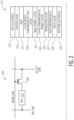
- FIG. 2 is a block diagram of an MRAM memory cell 201 according to one embodiment of the present invention that may be implemented in array 102 of system 101.
- Cell 201 includes a magnetic tunnel junction (MTJ) 211 and includes a select transistor 203 whose gate is connected to a wordline. When asserted, the wordline makes transistor 203 conductive to provide a path between the bit line of the column and the source line of the column through MTJ 211.
- MTJ 211 either provides a higher resistance indicating one memory state or a lower resistance indicating a second state.
- Figure 2 also shows a block diagram of MTJ 211.
- MTJ 211 has several layers located between bottom electrode 231 and top electrode 213.
- MTJ 211 is located in the interconnect portion of an integrated circuit between two metal layers where bottom electrode 231 is a portion of a metal interconnect in a lower metal layer and electrode 213 is a portion of a metal interconnect in an upper metal layer.
- the stack of layers of MTJ 211 are formed by the sequential deposition and patterning during the formation of the interconnect portion of an integrated circuit.
- each of the layers are patterned to have a cylindrical shape but may have other shapes in other embodiments.
- Located on bottom electrode 231 is a seed layer 229 which is deposited for the formation of an antiferromagnetic material layer 227, which in one embodiment is of a synthetic antiferromagnetic material.
- a transition layer 225 is located on layer 227.
- a ferromagnetic pinned layer 223, which in the embodiment shown is made of CoFeB, is located on layer 225.
- a ferromagnetic free layer 219 which in the embodiment shown is made of a CoFeB based ferromagnetic material, is located on tunnel layer 221.
- Layer 217 of MgO is located on free layer 219, and spacer layer 215 is located between layer 217 and electrode 213.
- Other embodiments may include MTJs of other configurations and/or made of other materials.
- the free layer and/or pin layer may include FeB and Ta.
- the free layer and/or pinned layer may be a composite layer of different materials.
- the magnetic polarization direction of the pinned layer 223 is fixed.
- the magnetic polarization direction of free layer 219 can be set to either a direction parallel to the magnetic polarization direction of the pinned layer 223 for a low resistive state or a direction anti parallel to the magnetic polarization direction of pinned layer 223 for a high resistive state.
- This type of MRAM cell is considered bi-stable in that there are only two detectable stable magnetic polarization directions of the free layer 219 with respect to the fixed layer 223 (parallel and antiparallel).
- the magnetic polarization direction of free layer 219 is set by providing a current at a sufficient magnitude through MTJ 211, where the direction of the current flow through MTJ 211 sets the magnetic polarization direction of the free layer 223 to the desired direction to store the desired value.
- MJTs of other embodiments may be written to or read from in other ways.
- the magnetic polarization direction of the pinned layer is fixed in the plane of the MTJ. In other embodiments, the magnetic polarization direction of the pinned layer is fixed perpendicular to the plane of the MTJ.
- the temperature dependent data retention error rate profile of an MTJ may depend upon several factors of an MTJ. For example, differences in the thickness of the ferromagnetic layers 219 and 223 and differences in the lateral cross-sectional area of the ferromagnetic layers 219 and 223 may affect the thermal stability and therefore the temperature range in which the free layer 219 is able to retain its programmed magnetic polarization direction. For example, a cell with a thinner free layer may make the cell more likely to retain its programmed state at a particular temperature than a similar cell with a thicker free layer.
- the cells of the different cell groups could be made with different lateral cross-sectional areas of the MTJs to provide for a different temperature dependent data retention error profile for each group. For example, cells with a greater lateral cross-sectional area of the MTJ would be more likely to retain its programmed state at a particular temperature than a similar cell with smaller lateral cross-sectional area.
- the lateral cross-sectional area of an MTJ or layer of an MTJ is the cross-sectional area of the MTJ or layer in a plane that is generally parallel with the interfacial areas between the layers of the MTJ.
- the lateral cross-sectional area of MTJ 211 is the area of the MTJ in a plane defined from left to right and into and out of the page, relative to the view of MTJ cell 211 in Figure 2 .
- the number of MgO layers of an MTJ may affect thermal stability of the cell.
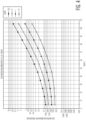
- FIG 3 is a chart showing a correlation between temperature exposure and data retention error rates for groups of cells according to one embodiment of the present invention.
- each of the five cell groups (113-117) (labeled CELLS A- CELLS E) have a different temperature dependent data retention error rate profile which provides for different data retention error rates when exposed to the same temperatures for the same period of time.
- the memory cells of group A have the high susceptibility to changing data states after being exposed at a particular temperature (are the least thermally stable) whereas the cells of group E have the lowest susceptibility to changing data states (are the most thermally stable).
- the MJTs of the cells of group E would have the largest lateral cross-sectional area and the MJTs of the cells of group A would have the smallest lateral cross-sectional area.
- the lateral cross-sectional areas of the MJTs of the cells of groups D, C, and B would be located in between.
- the free layer of the cells of group E would be the thinnest and the free layer of the cells of group A would be the thickest.
- the correlation between temperature exposure and data retention error is strongest for data retention error rates within a certain range.
- that range is between the HIGH VALID RATE (approximately 2.9 percent error rate) and the LOW VALID RATE (approximately 1.8 percent error rate).
- the system may determine temperature exposure from the error rate of the cell group or cell groups that fall in the valid error range. As shown in the graph of Figure 3 , for exposure temperatures between 51 and 67 degrees C, a system will use the error rate of the cells of group A to determine temperature exposure. For temperatures between 67 and 79 degrees C, the system will use the error rate of the cells of group B to determine temperature exposure.
- the system will use the cells of group C to determine temperature exposure.
- the system will use the cells of group D to determine temperature exposure.
- the system will use the cells of group E to determine temperature exposure.
- a system may use more than one group of cells to determine temperature exposure. For example, if two groups were to have an error rate within a valid error range, then the temperature exposure indicated by both groups would be averaged to obtain resultant temperature exposure data. In some embodiments, all the cells of the temperature exposure detection system have the same temperature dependent data retention error rate profile wherein temperature exposure data would be determined from just one curve.
- Figure 4 is a chart showing the relationship between data retention error rates of nonvolatile memory cells and temperature exposure and how those rates change based on the time after programming.
- the longer data is stored in a memory cell the greater the probability the data will flip states. As shown in the embodiment of Figure 4 , this increase in data retention error rates holds across all temperatures. Accordingly, a temperature exposure detection system may take into account the time from last programming in order to determine temperature exposure based on measured data retention error rates.
- temperature exposure information may be indicative of the highest temperature that a system is exposed to.
- temperature exposure information may indicate a cumulative amount of time of exposure at elevated temperatures. The amount of time that memory cells need to be exposed at a certain temperature for data retention error rates to rise may be a factor in what the temperature exposure information is indicative of.
- the cells of cell group A (113) may be more indicative of a peak temperature in that they are more susceptible to switching where the cells of group E (117) may be more indicative of a cumulative exposure to extreme temperatures.
- a short momentary exposure to a very high temperature may not be as harmful as a prolonged exposure at lower temperatures.
- Figure 5 sets forth a calibration routine for setting data retention error rate/ temperature exposure correlation information for a temperature exposure detection system according to one embodiment of the present invention.
- the system is exposed to a range of temperatures, where the data retention error rates are determined after exposure to each temperature by a read of the nonvolatile memory cells of the system.
- the test temperature (TESTTEMP) is set to the lowest temperature of the test range.
- the memory cells of the system are programmed to a predefined set of values, which in one embodiment is all 0s, but in other embodiments may be all 1s or a pattern of 1s and 0s.
- the cells are exposed to the TESTTEMP temperature for a predetermined period of time. Afterwards, the cells are read to determine the data retention error rate for each cell group. In one embodiment, the system reads all the cells of the array and compares the read values to the predefined values (e.g., all 0's) written in operation 505.
- the number of incorrect read bits of a cell group is divided by the total number of bits of the cell group to determine an error rate percentage for the cell group at that temperature.
- TESTTEMP is increased to the next temperature in the range in operation 513 and operations 505, 507 and 509 are performed again until all temperatures in the range have been tested.
- the test results are used to generate data retention error rates/temperature exposure correlation data for storing in a memory (e.g., tables 111) of a temperature exposure determination system.
- routine 501 would be performed after manufacturing and prior to sale of the system. In some embodiments, routine 501 would be performed on a small subset of manufactured systems where the resultant correlation data would be programmed into the memories of the other manufactured systems. In still other embodiments, initial correlation data would be programmed into the memory (e.g., tables 111) of a system. Afterwards, the system would be calibrated at one temperature, where the measured results at the one temperature would be used to adjust the initial correlation data programmed in the memory. In some embodiments (e.g., that utilize MRAM cells), initial correlation data may be obtained from switching models, where a thermal stability factor of the cells is extracted by extrapolation of off-state conditions, i.e., zero magnetic field, zero current and ambient temperature. In other embodiments, a system may be calibrated in other ways.
- initial correlation data may be obtained from switching models, where a thermal stability factor of the cells is extracted by extrapolation of off-state conditions, i.e., zero magnetic field, zero current and ambient temperature. In other embodiments
- Figure 6 is a flow chart of a routine 601 for determining temperature exposure by a temperature exposure detection system (e.g., 101) as per one embodiment of the present invention.
- system 101 receives a command (e.g., via RF receiver 103) to provide temperature exposure information.
- determination circuitry 105 preforms a read on all of the cells of array 102 and determines the data retention error rate for each cell group (113-117).
- determination circuitry 105 determines which cell group or groups of cell groups (113-117) has a data retention error rate within a valid range (e.g., 2.8-3.8% in Figure 3 ).
- determination circuitry 105 determines the temperature exposure information from the data retention error rate of the cell group(s) with data in the valid range.
- the temperature exposure information is provided to the requestor (e.g., controller 705 in Figure 7 ) e.g., via RF receiver 103.
- a temperature exposure monitoring system may determine and provide temperature exposure in other ways.
- Figure 7 is a block diagram showing temperature exposure detection system 101 being attached to an item 701 being monitored.
- Item 701 can be any product for which it is desirable to determine what temperatures the item has been exposed to.
- item 701 can be batteries, food, beverages, plastics, medicines, vaccines, chemical substances, or electronic equipment or components.
- Such information can be used in determining whether warranty or product usage conditions were complied with.
- the information may be used to determine the conditions that raw materials where subject to for determining whether to alter manufacturing processes.
- such information can be used to determine whether a product is nearing end of life or should be replaced.
- system 101 is implemented in a tag that is attached to the item or package container.
- system 101 may be part of the electronics of item 701.
- system 101 would be integrated with the package container such as enclosed within a liquid container.
- Controller 705 is used to program system 101 to begin monitoring temperature exposure, to request temperature exposure information regarding the item, and to reset system 101 to begin monitoring for a second period.
- controller 705 exchanges information with system 101 wirelessly, although in other embodiments, that information may be exchanged via a wired communication link (not shown).
- Controller 705 may be a portable device such as a handheld inventory scanner, laptop, or cell phone or it may a stationary device such as a scanner, manufacturing tool, or desktop computer.
- different devices may be used to program, read, and reset system 101.
- the some of the determination operations may be performed by controller 705.
- the different nonvolatile memory cell groups may be located in different integrated circuits of a temperature exposure detection system.
- system 101 can monitor temperature exposure even when not powered up. Accordingly, such a system can monitor temperature for items when they are not powered or for items that are not configured to be powered (e.g., food, liquids). Also, because the memory cells are reprogrammable, a system can be reused to monitor multiple items. For example, system 101 can be incorporated into a barrel and can be reset to monitor temperature each time the barrel is filled.
- a temperature exposure detection system includes a plurality of nonvolatile memory cells, read circuitry for reading the plurality of nonvolatile memory cells, and determination circuity that determines a data retention error rate of the plurality of nonvolatile memory cells based on a read of the plurality of nonvolatile memory cells and determines temperature exposure of the system based on the determined data retention error rate of at least some of the plurality of nonvolatile memory cells.
- a method of determining temperature exposure of a system includes reading a plurality of nonvolatile memory cells of the system, determining a data retention error rate of the plurality of nonvolatile memory cells based on a read of those memory cells, and determining temperature exposure of the system based on the determined data retention error rate of at least some of the plurality of nonvolatile memory cells.
Landscapes
- Physics & Mathematics (AREA)
- General Physics & Mathematics (AREA)
- Techniques For Improving Reliability Of Storages (AREA)
- For Increasing The Reliability Of Semiconductor Memories (AREA)
- Read Only Memory (AREA)
Abstract
Description
- This invention relates in general to temperature exposure detection based on memory cell data retention error rate.
- Nonvolatile memories are utilized for storing data including during times when the memory is not powered.
- The present invention may be better understood, and its numerous objects, features, and advantages made apparent to those skilled in the art by referencing the accompanying drawings.
-
Figure 1 is a circuit diagram of a temperature exposure detection system according to one embodiment of the present invention. -
Figure 2 is a schematic of an MRAM cell. -
Figure 3 is a chart showing a correlation between temperature exposure and retention error rates for cell groups according to one embodiment of the present invention. -
Figure 4 is a chart showing a correlation between temperature exposure and retention error rates over time according to one embodiment of the present invention. -
Figure 5 is a flow chart of a calibration routine for a temperature exposure detection system according to one embodiment of the present invention. -
Figure 6 is a flow chart of a routine for determining temperature exposure according to one embodiment of the present invention. -
Figure 7 is a block diagram of a temperature exposure monitoring system and a monitored item according to one embodiment of the present invention. - The use of the same reference symbols in different drawings indicates identical items unless otherwise noted. The Figures are not necessarily drawn to scale.
- The following sets forth a detailed description of a mode for carrying out the invention. The description is intended to be illustrative of the invention and should not be taken to be limiting.
- As disclosed herein, a temperature exposure detection system includes a plurality of nonvolatile memory cells. The memory includes memory read circuity for reading the plurality of memory cells to determine a data retention error rate of the plurality of memory cells. The temperature exposure detection system determines a temperature exposure of the system based on the determined data retention error rate
- In some embodiments, reading nonvolatile memory cells to determine a retention error rate that correlates to a particular temperature exposure profile may provide for a system that can monitor temperature exposure without having to be powered.
-
Figure 1 is a temperaturedisclosure detection system 101 according to one embodiment of the present invention.System 101 includes an array ofnonvolatile memory cells 102 that are arranged in rows and columns. In the embodiment shown,array 102 includes 5 subarray portions of cells (cell groups 113-117) where each subarray portion has cells with a different temperature dependent data retention error rate profile (A-E). A cells temperature dependent data retention error rate profile is based on physical aspects of the cell which define the cell's propensity to retain a stored data state over a range of exposed temperatures. -
System 101 includeswordline driver circuitry 107 which includes adecoder 109 and a plurality of wordline drivers each connected to a wordline (WLS A-WLS E) of a row ofarray 102.Circuitry 107 asserts a wordline to a row ofarray 102 to access memory cells of the row for a memory read or write operation. In the embodiment shown, wordlines WLS A are for accessing cells of a row in the sub array portion ofcell group 113, wordlines WLS B are for accessing cells of a row in the sub array portion ofcell group 114, wordlines WLS C are for accessing cells of a row in the sub array portion ofcell group 115, wordlines WLS D are for accessing cells of a row in the sub array portion of cell group 116, and wordlines WLS E are for accessing cells of a row in the sub array portion ofcell group 117.Decoder 109 receives a portion of a memory address (ADDRESS) fromdetermination circuitry 105 and activates the wordline driver ofcircuitry 107 corresponding to the received address to assert the wordline of the cells of the address. -
System 101 includes column mux and writecircuitry 119 for writing data to cells ofarray 102 for memory operations.Circuitry 119 receives a portion of an address (ADDRESS) fromdetermination circuitry 105 where a decoder ofcircuitry 119 controls column multiplexers ofcircuitry 119 to direct the columns of the cells of an address to the write circuitry ofcircuitry 119 to be written to during a memory operation. In the embodiment shown, the column multiplexers ofcircuitry 119 also direct the columns of the cells of an address to thesense amplifiers 120 for reading data of those cells during a read operation. - In the embodiment shown,
system 101 includes an M number ofsense amplifiers 120 for reading M number of cells during a data read operation. There are M number of N-to-1 column multiplexers incircuitry 119 for redirecting the columns to the sense amplifiers and write circuitry during read and write operations. M may be any number such as 8, 16, 32, 35, 64, 128 etc. N may be of one of a number such as 2, 8, 9, 12, 16, 32, 64 etc. Also,circuitry 119 may include termination circuitry for terminating the unselected columns during a read or write operation. In some embodiments,circuitry 119 would not include column multiplexers where every column would include its own sense amplifier. In one embodiment,array 102 has 500 rows were each group of cells 113-117 is located in 100 rows ofarray 102 which row having 100 cells, however the number rows and/or cells may be different in different embodiments. - In some embodiments, the specific circuitry implemented for
circuitry 119,sense amplifiers 120, andcircuitry 107 would depend upon the type of nonvolatile memory cells ofarray 102. In other embodiments, each group of cells 113-117 be located in a separate array with each array having a corresponding wordline driver circuity, column mux and write circuitry, and sense amplifiers. In some embodiments, the cells of the different groups would be located in different columns where the different cell groups would share the same wordlines. - In the embodiment shown,
determination circuitry 105 generates the ADDRESS values, memory operation commands (e.g., W/R), and write data (DATA IN) for performing a read or write memory operation.Circuitry 105 also receives the read data (DATA OUT) from the sense amplifiers (120) during a memory read operation. In the embodiment shown,circuity 105 includes a memory (tables 111) for storing data that correlates data retention error rates determined from the memory reads of each cell group with temperature exposure profiles of the cells groups. In some embodiments where only one data state is written (e.g., all 0s) during a programing operation, DATA IN lines would not be located betweencircuitry 105 andcircuitry 119. In such an embodiment, the write circuitry would be configured to place the cells in the single data state based on the write signal during a programming operation. - In some embodiments,
circuitry 105 may include a processor core for performing the write operations, read operations, and for determining the temperature exposure information based on the read values. In other embodiments,circuitry 105 may include discrete circuitry (e.g., counters, comparators, adders, shifters) for performing at least some of the operations. In still other embodiments,circuity 105 may include a combination of both processor cores and discrete circuitry. Also, in some embodiments, determination circuitry may include circuitry that performs other operations for a system that includessystem 101 such as a system controller. In some embodiments,circuitry 105 may include a processor core for performing the memory operations and a separate processor core for determining the temperature exposure information. In some embodiments, the different processor cores (or discrete circuitry) may be located on different integrated circuits or in different component housings. - In the embodiment shown,
system 101 includes atransceiver 103 for communicating wirelessly with a controller (e.g.,controller 705 inFigure 7 ) for receiving commands to provide temperature exposure information and to program the system. Transceiver 103 also provides the temperature exposure information wirelessly to the controller. In other embodiments,system 101 would include I/O circuitry for receiving and providing data by a wired connection with a controller. - Examples of nonvolatile memory types cells utilized in
system 101 include MRAM, ReRAM, FeRAM, flash, or phase change memories. In some embodiments, all of the memory cells ofsystem 101 would be the same memory cell type. However, systems of other embodiments may include cells of more than one memory cell type. In some embodiments, memory cell types that have a temperature dependent data retention error rate profile where data retention varies widely with temperature exposure may be better suited for use in a temperature exposure detection monitoring system. - In some embodiments,
system 101 may include memory cells characterized as bi-stable memory cells. With bi-stable memory cells, the cell generally resides at one of two stable memory states. For example, with some MRAM cells, the cell will be stable in either one memory state or another memory state, depending upon the magnetic polarization of the ferromagnetic free layer of the magnetic tunnel junction of the MRAM cell. SeeFigure 2 and its corresponding description. Another type of bi-stable nonvolatile memory cell is an FeRAM memory cell. - In some embodiments, using data retention error rates as measured by memory reads to determine temperature exposure information may advantageously be useful for bi-stable nonvolatile memory cell types in that a specific degree of temperature exposure of the material of a specific memory cell cannot be easily measured due to the bi-state nature of the cell. In some embodiments, utilizing bi-stable cells over other types of memory cells may allow for a data retention error rate determination to be made by a less complicated process in that it may be performed digitally in a more simplified manner.
-
Figure 2 is a block diagram of anMRAM memory cell 201 according to one embodiment of the present invention that may be implemented inarray 102 ofsystem 101.Cell 201 includes a magnetic tunnel junction (MTJ) 211 and includes aselect transistor 203 whose gate is connected to a wordline. When asserted, the wordline makestransistor 203 conductive to provide a path between the bit line of the column and the source line of the column throughMTJ 211. Depending upon the storage state ofMTJ 211,MTJ 211 either provides a higher resistance indicating one memory state or a lower resistance indicating a second state. -
Figure 2 also shows a block diagram ofMTJ 211. In the embodiment shown,MTJ 211 has several layers located betweenbottom electrode 231 andtop electrode 213. In one embodiment,MTJ 211 is located in the interconnect portion of an integrated circuit between two metal layers wherebottom electrode 231 is a portion of a metal interconnect in a lower metal layer andelectrode 213 is a portion of a metal interconnect in an upper metal layer. - In one embodiment, the stack of layers of
MTJ 211 are formed by the sequential deposition and patterning during the formation of the interconnect portion of an integrated circuit. In one embodiment, each of the layers are patterned to have a cylindrical shape but may have other shapes in other embodiments. Located onbottom electrode 231 is a seed layer 229 which is deposited for the formation of an antiferromagnetic material layer 227, which in one embodiment is of a synthetic antiferromagnetic material. A transition layer 225 is located on layer 227. A ferromagnetic pinnedlayer 223, which in the embodiment shown is made of CoFeB, is located on layer 225. Atunnel layer 221, which in the embodiment shown in made of MgO, is located on pinnedlayer 223. A ferromagneticfree layer 219, which in the embodiment shown is made of a CoFeB based ferromagnetic material, is located ontunnel layer 221.Layer 217 of MgO is located onfree layer 219, andspacer layer 215 is located betweenlayer 217 andelectrode 213. Other embodiments may include MTJs of other configurations and/or made of other materials. For example, in some embodiments, the free layer and/or pin layer may include FeB and Ta. In some embodiments, the free layer and/or pinned layer may be a composite layer of different materials. - In some embodiments, the magnetic polarization direction of the pinned
layer 223 is fixed. The magnetic polarization direction offree layer 219 can be set to either a direction parallel to the magnetic polarization direction of the pinnedlayer 223 for a low resistive state or a direction anti parallel to the magnetic polarization direction of pinnedlayer 223 for a high resistive state. This type of MRAM cell is considered bi-stable in that there are only two detectable stable magnetic polarization directions of thefree layer 219 with respect to the fixed layer 223 (parallel and antiparallel). In some embodiments, the magnetic polarization direction offree layer 219 is set by providing a current at a sufficient magnitude throughMTJ 211, where the direction of the current flow throughMTJ 211 sets the magnetic polarization direction of thefree layer 223 to the desired direction to store the desired value. MJTs of other embodiments may be written to or read from in other ways. In some embodiments, the magnetic polarization direction of the pinned layer is fixed in the plane of the MTJ. In other embodiments, the magnetic polarization direction of the pinned layer is fixed perpendicular to the plane of the MTJ. - The temperature dependent data retention error rate profile of an MTJ (the propensity of the cell to retain its programmed magnetic state and therefore its programmed data over a range of temperatures) may depend upon several factors of an MTJ. For example, differences in the thickness of the
ferromagnetic layers ferromagnetic layers free layer 219 is able to retain its programmed magnetic polarization direction. For example, a cell with a thinner free layer may make the cell more likely to retain its programmed state at a particular temperature than a similar cell with a thicker free layer. In other embodiments, the cells of the different cell groups (113-117) could be made with different lateral cross-sectional areas of the MTJs to provide for a different temperature dependent data retention error profile for each group. For example, cells with a greater lateral cross-sectional area of the MTJ would be more likely to retain its programmed state at a particular temperature than a similar cell with smaller lateral cross-sectional area. In some embodiments, the lateral cross-sectional area of an MTJ or layer of an MTJ is the cross-sectional area of the MTJ or layer in a plane that is generally parallel with the interfacial areas between the layers of the MTJ. In the embodiment ofFigure 2 , the lateral cross-sectional area ofMTJ 211 is the area of the MTJ in a plane defined from left to right and into and out of the page, relative to the view ofMTJ cell 211 inFigure 2 . In other embodiments, the number of MgO layers of an MTJ may affect thermal stability of the cell. -
Figure 3 is a chart showing a correlation between temperature exposure and data retention error rates for groups of cells according to one embodiment of the present invention. As shown inFigure 3 , each of the five cell groups (113-117) (labeled CELLS A- CELLS E) have a different temperature dependent data retention error rate profile which provides for different data retention error rates when exposed to the same temperatures for the same period of time. As shown inFigure 3 , the memory cells of group A have the high susceptibility to changing data states after being exposed at a particular temperature (are the least thermally stable) whereas the cells of group E have the lowest susceptibility to changing data states (are the most thermally stable). - In one embodiment, the MJTs of the cells of group E would have the largest lateral cross-sectional area and the MJTs of the cells of group A would have the smallest lateral cross-sectional area. The lateral cross-sectional areas of the MJTs of the cells of groups D, C, and B would be located in between. In another embodiment, the free layer of the cells of group E would be the thinnest and the free layer of the cells of group A would be the thickest.
- As shown in the graph of
Figure 3 , as the cells are exposed to higher temperatures, the data retention error rate rise. Accordingly, by measuring the data retention error rate by performing data reads of programmed data stored in the cells, an indication can made as to the temperatures that the cells were exposed to. - In some embodiments, the correlation between temperature exposure and data retention error is strongest for data retention error rates within a certain range. In the embodiment shown in
Figure 3 , that range is between the HIGH VALID RATE (approximately 2.9 percent error rate) and the LOW VALID RATE (approximately 1.8 percent error rate). Accordingly, in some embodiments of a system with multiple cell groups, the system may determine temperature exposure from the error rate of the cell group or cell groups that fall in the valid error range. As shown in the graph ofFigure 3 , for exposure temperatures between 51 and 67 degrees C, a system will use the error rate of the cells of group A to determine temperature exposure. For temperatures between 67 and 79 degrees C, the system will use the error rate of the cells of group B to determine temperature exposure. For temperatures between 79 and 89 C, the system will use the cells of group C to determine temperature exposure. For temperatures between 89 and 99 degrees C, the system will use the cells of group D to determine temperature exposure. For temperatures between 99 and 109 degrees C, the system will use the cells of group E to determine temperature exposure. - In some embodiments, a system may use more than one group of cells to determine temperature exposure. For example, if two groups were to have an error rate within a valid error range, then the temperature exposure indicated by both groups would be averaged to obtain resultant temperature exposure data. In some embodiments, all the cells of the temperature exposure detection system have the same temperature dependent data retention error rate profile wherein temperature exposure data would be determined from just one curve.
-
Figure 4 is a chart showing the relationship between data retention error rates of nonvolatile memory cells and temperature exposure and how those rates change based on the time after programming. In some embodiments, the longer data is stored in a memory cell, the greater the probability the data will flip states. As shown in the embodiment ofFigure 4 , this increase in data retention error rates holds across all temperatures. Accordingly, a temperature exposure detection system may take into account the time from last programming in order to determine temperature exposure based on measured data retention error rates. - In some embodiments, temperature exposure information may be indicative of the highest temperature that a system is exposed to. In other embodiments, temperature exposure information may indicate a cumulative amount of time of exposure at elevated temperatures. The amount of time that memory cells need to be exposed at a certain temperature for data retention error rates to rise may be a factor in what the temperature exposure information is indicative of. In some embodiments, the cells of cell group A (113) may be more indicative of a peak temperature in that they are more susceptible to switching where the cells of group E (117) may be more indicative of a cumulative exposure to extreme temperatures.
- With some items being monitored, a short momentary exposure to a very high temperature may not be as harmful as a prolonged exposure at lower temperatures. In some embodiments, it may be desirable to closely match the temperature dependent data retention error rate profiles of the cells of a system with the harmful temperature exposure profile of the products being monitored at least for the valid ranges of data retention error rates.
-
Figure 5 sets forth a calibration routine for setting data retention error rate/ temperature exposure correlation information for a temperature exposure detection system according to one embodiment of the present invention. During the routine, the system is exposed to a range of temperatures, where the data retention error rates are determined after exposure to each temperature by a read of the nonvolatile memory cells of the system. - At
operation 503, the test temperature (TESTTEMP) is set to the lowest temperature of the test range. Inoperation 505, the memory cells of the system are programmed to a predefined set of values, which in one embodiment is all 0s, but in other embodiments may be all 1s or a pattern of 1s and 0s. Inoperation 507, the cells are exposed to the TESTTEMP temperature for a predetermined period of time. Afterwards, the cells are read to determine the data retention error rate for each cell group. In one embodiment, the system reads all the cells of the array and compares the read values to the predefined values (e.g., all 0's) written inoperation 505. The number of incorrect read bits of a cell group is divided by the total number of bits of the cell group to determine an error rate percentage for the cell group at that temperature. Inoperation 511, if not all of the temperatures of the range have been tested, TESTTEMP is increased to the next temperature in the range inoperation 513 andoperations operation 515, the test results are used to generate data retention error rates/temperature exposure correlation data for storing in a memory (e.g., tables 111) of a temperature exposure determination system. - In some embodiments, routine 501 would be performed after manufacturing and prior to sale of the system. In some embodiments, routine 501 would be performed on a small subset of manufactured systems where the resultant correlation data would be programmed into the memories of the other manufactured systems. In still other embodiments, initial correlation data would be programmed into the memory (e.g., tables 111) of a system. Afterwards, the system would be calibrated at one temperature, where the measured results at the one temperature would be used to adjust the initial correlation data programmed in the memory. In some embodiments (e.g., that utilize MRAM cells), initial correlation data may be obtained from switching models, where a thermal stability factor of the cells is extracted by extrapolation of off-state conditions, i.e., zero magnetic field, zero current and ambient temperature. In other embodiments, a system may be calibrated in other ways.
-
Figure 6 is a flow chart of a routine 601 for determining temperature exposure by a temperature exposure detection system (e.g., 101) as per one embodiment of the present invention. Inoperation 603,system 101 receives a command (e.g., via RF receiver 103) to provide temperature exposure information. Inoperation 605,determination circuitry 105 preforms a read on all of the cells ofarray 102 and determines the data retention error rate for each cell group (113-117). Inoperation 607,determination circuitry 105 determines which cell group or groups of cell groups (113-117) has a data retention error rate within a valid range (e.g., 2.8-3.8% inFigure 3 ). Inoperation 609,determination circuitry 105 determines the temperature exposure information from the data retention error rate of the cell group(s) with data in the valid range. Inoperation 611, the temperature exposure information is provided to the requestor (e.g.,controller 705 inFigure 7 ) e.g., viaRF receiver 103. In other embodiments, a temperature exposure monitoring system may determine and provide temperature exposure in other ways. -
Figure 7 is a block diagram showing temperatureexposure detection system 101 being attached to anitem 701 being monitored.Item 701 can be any product for which it is desirable to determine what temperatures the item has been exposed to. For example,item 701 can be batteries, food, beverages, plastics, medicines, vaccines, chemical substances, or electronic equipment or components. For some products, it may be desirable to determine temperatures that an item was exposed to prior to the sale of the item e.g., as when an item is sitting in a warehouse or during transit. Such information can be used in determining whether warranty or product usage conditions were complied with. In other embodiments, the information may be used to determine the conditions that raw materials where subject to for determining whether to alter manufacturing processes. In other embodiments, such information can be used to determine whether a product is nearing end of life or should be replaced. - In one embodiment,
system 101 is implemented in a tag that is attached to the item or package container. In other embodiments,system 101 may be part of the electronics ofitem 701. In still other embodiments,system 101 would be integrated with the package container such as enclosed within a liquid container. -
Controller 705 is used toprogram system 101 to begin monitoring temperature exposure, to request temperature exposure information regarding the item, and to resetsystem 101 to begin monitoring for a second period. In the embodiment shown,controller 705 exchanges information withsystem 101 wirelessly, although in other embodiments, that information may be exchanged via a wired communication link (not shown).Controller 705 may be a portable device such as a handheld inventory scanner, laptop, or cell phone or it may a stationary device such as a scanner, manufacturing tool, or desktop computer. In some embodiments, different devices may be used to program, read, and resetsystem 101. In some embodiments, the some of the determination operations may be performed bycontroller 705. In some embodiments, the different nonvolatile memory cell groups may be located in different integrated circuits of a temperature exposure detection system. - In some embodiments, because
system 101 utilizes nonvolatile memory cells to determine temperature exposure of an item,system 101 can monitor temperature exposure even when not powered up. Accordingly, such a system can monitor temperature for items when they are not powered or for items that are not configured to be powered (e.g., food, liquids). Also, because the memory cells are reprogrammable, a system can be reused to monitor multiple items. For example,system 101 can be incorporated into a barrel and can be reset to monitor temperature each time the barrel is filled. - Features specifically shown or described with respect to one embodiment set forth herein may be implemented in other embodiments set forth herein.
- In one embodiment, a temperature exposure detection system includes a plurality of nonvolatile memory cells, read circuitry for reading the plurality of nonvolatile memory cells, and determination circuity that determines a data retention error rate of the plurality of nonvolatile memory cells based on a read of the plurality of nonvolatile memory cells and determines temperature exposure of the system based on the determined data retention error rate of at least some of the plurality of nonvolatile memory cells.
- In another embodiment, a method of determining temperature exposure of a system, includes reading a plurality of nonvolatile memory cells of the system, determining a data retention error rate of the plurality of nonvolatile memory cells based on a read of those memory cells, and determining temperature exposure of the system based on the determined data retention error rate of at least some of the plurality of nonvolatile memory cells.
- While particular embodiments of the present invention have been shown and described, it will be recognized to those skilled in the art that, based upon the teachings herein, further changes and modifications may be made without departing from this invention and its broader aspects, and thus, the appended claims are to encompass within their scope all such changes and modifications as are within the true spirit and scope of this invention.
Claims (15)
- A temperature exposure detection system comprising:a plurality of nonvolatile memory cells;read circuitry for reading the plurality of nonvolatile memory cells;determination circuity that determines a data retention error rate of the plurality of nonvolatile memory cells based on a read of the plurality of nonvolatile memory cells and determines temperature exposure of the system based on the determined data retention error rate of at least some of the plurality of nonvolatile memory cells.
- The system of claim 1 further wherein each of the plurality of nonvolatile memory cells is characterized as a bi-stable state memory cell.
- The system of claim 1 or 2, wherein the memory cells of the plurality of nonvolatile memory cells are characterized as MRAM cells.
- The system of any preceding claim, wherein the memory cells of the plurality of nonvolatile memory cells are characterized as FeRAM cells.
- The system of any preceding claim, wherein the plurality of nonvolatile memory cells includes a plurality of groups of memory cells, wherein memory cells of each group of the plurality of groups have a different temperature dependent data retention error rate profile than memory cells of the other groups of the plurality of groups.
- The system of claim 5 wherein memory cells of each group of the plurality of groups have a layer with a thickness that is different than a thickness of a corresponding layer in memory cells of the other groups of the plurality of groups.
- The system of claim 5 or 6,wherein memory cells of each group of the plurality of groups have a structure with a lateral cross-sectional area that is different than a lateral cross-sectional area of a corresponding structure in memory cells of the other groups of the plurality of groups.
- The system of claim 7 wherein the structure is characterized as at least a portion of an MTJ of an MRAM cell.
- The system of any one of claims 5 to 8, wherein the determination circuity determines the temperature exposure of the system based on the determined data retention error rate of at least one group of the plurality that is determined to have a retention error rate within a particular retention error rate range.
- The system of any preceding claim, wherein the determination circuity determines the temperature exposure of the system based on an amount of time that specific data has been stored in the at least some of the plurality of nonvolatile memory cells.
- The system of any preceding claim, wherein the temperature exposure of the system is indicative of an amount of time that the system has been exposed to a temperature that meets or exceeds a particular temperature threshold value.
- The system of any preceding claim, wherein the determination circuitry includes a memory with a plurality of temperature exposure values correlated with data retention error rate values for memory cells of the plurality of nonvolatile memory cells.
- The system of claim 12 wherein a correlation of the plurality of temperature exposure values with the data retention error rate values in the memory is based on a calibration procedure of the system which exposes the system to at least one temperature and determining a data retention error rate of at least some of the plurality of nonvolatile memory cells after an exposure to the at least one temperature.
- A method of determining temperature exposure of a system, the method comprising:reading a plurality of nonvolatile memory cells of the system;determining a data retention error rate of the plurality of nonvolatile memory cells based on a read of those memory cells;determining temperature exposure of the system based on the determined data retention error rate of at least some of the plurality of nonvolatile memory cells.
- The method of claim 14 wherein the memory cells of the plurality of nonvolatile memory cells are characterized as MRAM cells.
Applications Claiming Priority (1)
| Application Number | Priority Date | Filing Date | Title |
|---|---|---|---|
| US17/405,633 US11670394B2 (en) | 2021-08-18 | 2021-08-18 | Temperature exposure detection based on memory cell retention error rate |
Publications (2)
| Publication Number | Publication Date |
|---|---|
| EP4137791A1 true EP4137791A1 (en) | 2023-02-22 |
| EP4137791B1 EP4137791B1 (en) | 2024-09-18 |
Family
ID=82116997
Family Applications (1)
| Application Number | Title | Priority Date | Filing Date |
|---|---|---|---|
| EP22179883.8A Active EP4137791B1 (en) | 2021-08-18 | 2022-06-20 | Temperature exposure detection based on memory cell retention error rate |
Country Status (3)
| Country | Link |
|---|---|
| US (1) | US11670394B2 (en) |
| EP (1) | EP4137791B1 (en) |
| CN (1) | CN115910186A (en) |
Families Citing this family (3)
| Publication number | Priority date | Publication date | Assignee | Title |
|---|---|---|---|---|
| KR20250016815A (en) | 2023-07-26 | 2025-02-04 | 삼성전자주식회사 | Storage device and method of providing exposure temperature of a nonvolatile memory device in power-off state |
| WO2025253914A1 (en) * | 2024-06-05 | 2025-12-11 | ソニーセミコンダクタソリューションズ株式会社 | Detection circuit and sensor device |
| WO2026053770A1 (en) * | 2024-09-09 | 2026-03-12 | ソニーセミコンダクタソリューションズ株式会社 | Sensor device |
Citations (2)
| Publication number | Priority date | Publication date | Assignee | Title |
|---|---|---|---|---|
| US20150052416A1 (en) * | 2013-08-16 | 2015-02-19 | Seagate Technology Llc | Determining Data Retention Time in a Solid-State Non-Volatile Memory |
| US20160027523A1 (en) * | 2013-07-29 | 2016-01-28 | Western Digital Technologies, Inc. | Data retention monitoring using temperature history in solid state drives |
Family Cites Families (51)
| Publication number | Priority date | Publication date | Assignee | Title |
|---|---|---|---|---|
| US6162684A (en) * | 1999-03-11 | 2000-12-19 | Advanced Micro Devices, Inc. | Ammonia annealed and wet oxidized LPCVD oxide to replace ono films for high integrated flash memory devices |
| DE10040890C1 (en) * | 2000-08-18 | 2002-01-31 | Trw Automotive Electron & Comp | System for safe high temperature flash memory operation in vehicle involves programming memory before high temperature operation so that each record is stored redundantly |
| KR100475590B1 (en) | 2002-11-13 | 2005-03-11 | 김영호 | Thin-film temperature sensor using chalcogenide glass semiconductor and method for manufacturing the same |
| EP1893961A4 (en) | 2005-06-21 | 2008-07-02 | Cornerstone Res Group Inc | Environmental condition cumulative tracking integration sensor using shape memory polymer |
| US7510883B2 (en) | 2005-09-30 | 2009-03-31 | Everspin Technologies, Inc. | Magnetic tunnel junction temperature sensors and methods |
| JP2007184419A (en) * | 2006-01-06 | 2007-07-19 | Sharp Corp | Nonvolatile memory device |
| US7583535B2 (en) * | 2006-12-30 | 2009-09-01 | Sandisk Corporation | Biasing non-volatile storage to compensate for temperature variations |
| US8213255B2 (en) * | 2010-02-19 | 2012-07-03 | Sandisk Technologies Inc. | Non-volatile storage with temperature compensation based on neighbor state information |
| US9021319B2 (en) * | 2011-09-02 | 2015-04-28 | SMART Storage Systems, Inc. | Non-volatile memory management system with load leveling and method of operation thereof |
| US8611157B2 (en) * | 2011-12-22 | 2013-12-17 | Sandisk Technologies Inc. | Program temperature dependent read |
| JP2014035673A (en) * | 2012-08-09 | 2014-02-24 | Renesas Electronics Corp | Semiconductor memory device and method |
| US9123445B2 (en) * | 2013-01-22 | 2015-09-01 | SMART Storage Systems, Inc. | Storage control system with data management mechanism and method of operation thereof |
| JP6022377B2 (en) * | 2013-02-28 | 2016-11-09 | ルネサスエレクトロニクス株式会社 | Manufacturing method of semiconductor device |
| US9007842B2 (en) * | 2013-03-12 | 2015-04-14 | Seagate Technology Llc | Retention detection and/or channel tracking policy in a flash memory based storage system |
| US9165683B2 (en) * | 2013-09-23 | 2015-10-20 | Sandisk Technologies Inc. | Multi-word line erratic programming detection |
| WO2015106162A1 (en) * | 2014-01-09 | 2015-07-16 | SanDisk Technologies, Inc. | Selective copyback for on die buffered non-volatile memory |
| US9330790B2 (en) * | 2014-04-25 | 2016-05-03 | Seagate Technology Llc | Temperature tracking to manage threshold voltages in a memory |
| EP2957879B1 (en) | 2014-06-16 | 2018-04-11 | Nxp B.V. | Temperature monitoring |
| US20170229176A1 (en) * | 2014-09-19 | 2017-08-10 | Hitach, Ltd. | Semiconductor storage device, and storage device using same |
| US9729534B2 (en) * | 2015-02-26 | 2017-08-08 | Seagate Technology Llc | In situ device authentication and diagnostic repair in a host environment |
| US9536619B2 (en) * | 2015-05-27 | 2017-01-03 | Kabushiki Kaisha Toshiba | Hybrid-HDD with improved data retention |
| US10048898B2 (en) * | 2015-06-15 | 2018-08-14 | Sandisk Technologies Llc | Data retention in a memory block based on local heating |
| US9891275B2 (en) * | 2015-06-24 | 2018-02-13 | International Business Machines Corporation | Integrated circuit chip reliability qualification using a sample-specific expected fail rate |
| US10228990B2 (en) * | 2015-11-12 | 2019-03-12 | Sandisk Technologies Llc | Variable-term error metrics adjustment |
| US10228872B2 (en) * | 2016-03-10 | 2019-03-12 | Toshiba Memory Corporation | Semiconductor device, and information-processing device |
| JP6203312B2 (en) * | 2016-03-16 | 2017-09-27 | 株式会社東芝 | Magnetic memory |
| EP3480698B1 (en) * | 2016-06-28 | 2020-12-09 | Nippon Seiki Co., Ltd. | Display device for vehicle |
| CN107768515B (en) * | 2016-08-18 | 2020-05-08 | 华邦电子股份有限公司 | Method for forming memory device |
| TWI626657B (en) * | 2016-11-10 | 2018-06-11 | 宜鼎國際股份有限公司 | Method for extending period of data retention of flash memory and device for the same |
| US9881682B1 (en) * | 2016-11-23 | 2018-01-30 | Seagate Technology Llc | Fine grained data retention monitoring in solid state drives |
| US10185609B2 (en) * | 2016-12-22 | 2019-01-22 | Smart Modular Technologies, Inc. | Virtual timer for data retention |
| US10468117B2 (en) * | 2017-01-12 | 2019-11-05 | Sandisk Technologies Llc | Read threshold adjustment with feedback information from error recovery |
| US11237908B2 (en) * | 2017-03-29 | 2022-02-01 | SK Hynix Inc. | Memory system and operating method thereof |
| US10403377B2 (en) * | 2017-06-26 | 2019-09-03 | Western Digital Technologies, Inc. | Non-volatile storage with adaptive redundancy |
| US10387281B2 (en) * | 2017-08-30 | 2019-08-20 | Micron Technology, Inc. | Flash memory block retirement policy |
| US10147876B1 (en) * | 2017-08-31 | 2018-12-04 | Sandisk Technologies Llc | Phase change memory electrode with multiple thermal interfaces |
| US10410730B1 (en) * | 2018-03-30 | 2019-09-10 | Qualcomm Incorporated | Selectively synchronizing flash memory block refreshes based in part upon memory block temperature |
| US10678449B2 (en) * | 2018-05-03 | 2020-06-09 | Microsoft Technology, LLC | Increasing flash memory retention time using waste heat |
| US10529400B1 (en) | 2018-07-27 | 2020-01-07 | Nxp Usa, Inc. | Magnetic attack detection in a magnetic random access memory (MRAM) |
| US11137808B2 (en) * | 2018-08-31 | 2021-10-05 | Micron Technology, Inc. | Temperature compensation in a memory system |
| US10983883B2 (en) * | 2019-03-27 | 2021-04-20 | Spin Memory, Inc. | Error recovery in magnetic random access memory after reflow soldering |
| US10892025B2 (en) * | 2019-06-13 | 2021-01-12 | Western Digital Technologies, Inc. | Soft erase and programming of nonvolatile memory |
| US11029889B1 (en) * | 2019-12-20 | 2021-06-08 | Western Digital Technologies, Inc. | Soft bit read mode selection for non-volatile memory |
| US11056211B1 (en) * | 2020-01-08 | 2021-07-06 | Western Digital Technologies, Inc. | Apparatus and method for handling temperature dependent failures in a memory device |
| US11385984B2 (en) * | 2020-02-24 | 2022-07-12 | Western Digital Technologies, Inc. | Variable read scan for solid-state storage device quality of service |
| US10978130B1 (en) * | 2020-03-25 | 2021-04-13 | Micron Technology, Inc. | Temperature-based access timing for a memory device |
| US11210031B1 (en) * | 2020-07-08 | 2021-12-28 | Western Digital Technologies, Inc. | Thermal region tags and thermal region outlier detection |
| US11416388B2 (en) * | 2020-09-22 | 2022-08-16 | Micron Technology, Inc. | Memory sub-system logical block address remapping |
| US11309036B1 (en) * | 2020-10-14 | 2022-04-19 | Dell Products L.P. | Systems and methods of implementing a calibration wordline to compensate for voltage threshold shift in NAND flash memory |
| US11956954B2 (en) * | 2020-11-09 | 2024-04-09 | Micron Technology, Inc. | Electronic devices comprising reduced charge confinement regions in storage nodes of pillars and related methods |
| US11422825B2 (en) * | 2020-12-30 | 2022-08-23 | Kioxia Corporation | Determination of power-off duration of NVMe SSD |
-
2021
- 2021-08-18 US US17/405,633 patent/US11670394B2/en active Active
-
2022
- 2022-06-20 EP EP22179883.8A patent/EP4137791B1/en active Active
- 2022-08-17 CN CN202210989736.0A patent/CN115910186A/en active Pending
Patent Citations (2)
| Publication number | Priority date | Publication date | Assignee | Title |
|---|---|---|---|---|
| US20160027523A1 (en) * | 2013-07-29 | 2016-01-28 | Western Digital Technologies, Inc. | Data retention monitoring using temperature history in solid state drives |
| US20150052416A1 (en) * | 2013-08-16 | 2015-02-19 | Seagate Technology Llc | Determining Data Retention Time in a Solid-State Non-Volatile Memory |
Also Published As
| Publication number | Publication date |
|---|---|
| EP4137791B1 (en) | 2024-09-18 |
| US20230056133A1 (en) | 2023-02-23 |
| US11670394B2 (en) | 2023-06-06 |
| CN115910186A (en) | 2023-04-04 |
Similar Documents
| Publication | Publication Date | Title |
|---|---|---|
| EP4137791B1 (en) | Temperature exposure detection based on memory cell retention error rate | |
| US11630724B2 (en) | Memory controller including ECC circuit, memory system having the same, and method of operating memory system and memory controller | |
| US8908413B2 (en) | Programmable resistance memory | |
| US9646685B2 (en) | Resistive memory device, resistive memory, and operating method of the resistive memory device | |
| EP3599608B1 (en) | Magnetic attack detection in a magnetic random access memory (mram) | |
| US7843741B2 (en) | Memory devices with selective pre-write verification and methods of operation thereof | |
| US8830728B2 (en) | Resistance change memory device and current trimming method thereof | |
| US7646625B2 (en) | Conditioning operations for memory cells | |
| CN105632558B (en) | Memory device including multi-level cell and method of operating the same | |
| KR101545512B1 (en) | Semiconductor memory apparatus, verify read method and system | |
| JP2022545716A (en) | Error correction for associative memory | |
| US9646660B2 (en) | Selectable memory access time | |
| JP2003022668A (en) | Resistive cross point memory with on-chip amplifier calibration method | |
| US11450358B2 (en) | On-the-fly programming and verifying method for memory cells based on counters and ECC feedback | |
| US10204037B2 (en) | Memory device, memory controller and operation method thereof | |
| TWI623939B (en) | Memory device and control method thereof | |
| EP3886103B1 (en) | Multi-level cell (mlc) cross-point memory | |
| US8750062B2 (en) | Memory element and method for determining the data state of a memory element | |
| CN113539346B (en) | Detection circuit for detecting memory array level | |
| US20240393961A1 (en) | Memory device with data scrubbing capability and methods | |
| US20230117173A1 (en) | Multi-command memory accesses | |
| KR20140101638A (en) | Semiconductor memory apparatus, read method and system |
Legal Events
| Date | Code | Title | Description |
|---|---|---|---|
| PUAI | Public reference made under article 153(3) epc to a published international application that has entered the european phase |
Free format text: ORIGINAL CODE: 0009012 |
|
| STAA | Information on the status of an ep patent application or granted ep patent |
Free format text: STATUS: THE APPLICATION HAS BEEN PUBLISHED |
|
| AK | Designated contracting states |
Kind code of ref document: A1 Designated state(s): AL AT BE BG CH CY CZ DE DK EE ES FI FR GB GR HR HU IE IS IT LI LT LU LV MC MK MT NL NO PL PT RO RS SE SI SK SM TR |
|
| STAA | Information on the status of an ep patent application or granted ep patent |
Free format text: STATUS: REQUEST FOR EXAMINATION WAS MADE |
|
| 17P | Request for examination filed |
Effective date: 20230822 |
|
| RBV | Designated contracting states (corrected) |
Designated state(s): AL AT BE BG CH CY CZ DE DK EE ES FI FR GB GR HR HU IE IS IT LI LT LU LV MC MK MT NL NO PL PT RO RS SE SI SK SM TR |
|
| GRAP | Despatch of communication of intention to grant a patent |
Free format text: ORIGINAL CODE: EPIDOSNIGR1 |
|
| STAA | Information on the status of an ep patent application or granted ep patent |
Free format text: STATUS: GRANT OF PATENT IS INTENDED |
|
| RIC1 | Information provided on ipc code assigned before grant |
Ipc: G11C 16/34 20060101ALI20240607BHEP Ipc: G11C 11/16 20060101ALI20240607BHEP Ipc: G11C 7/04 20060101ALI20240607BHEP Ipc: G11C 11/00 20060101ALI20240607BHEP Ipc: G01K 7/36 20060101ALI20240607BHEP Ipc: G01K 3/04 20060101ALI20240607BHEP Ipc: G01K 3/00 20060101AFI20240607BHEP |
|
| INTG | Intention to grant announced |
Effective date: 20240624 |
|
| GRAS | Grant fee paid |
Free format text: ORIGINAL CODE: EPIDOSNIGR3 |
|
| GRAA | (expected) grant |
Free format text: ORIGINAL CODE: 0009210 |
|
| STAA | Information on the status of an ep patent application or granted ep patent |
Free format text: STATUS: THE PATENT HAS BEEN GRANTED |
|
| AK | Designated contracting states |
Kind code of ref document: B1 Designated state(s): AL AT BE BG CH CY CZ DE DK EE ES FI FR GB GR HR HU IE IS IT LI LT LU LV MC MK MT NL NO PL PT RO RS SE SI SK SM TR |
|
| REG | Reference to a national code |
Ref country code: GB Ref legal event code: FG4D |
|
| REG | Reference to a national code |
Ref country code: CH Ref legal event code: EP |
|
| REG | Reference to a national code |
Ref country code: IE Ref legal event code: FG4D |
|
| REG | Reference to a national code |
Ref country code: DE Ref legal event code: R096 Ref document number: 602022006149 Country of ref document: DE |
|
| REG | Reference to a national code |
Ref country code: LT Ref legal event code: MG9D |
|
| PG25 | Lapsed in a contracting state [announced via postgrant information from national office to epo] |
Ref country code: NO Free format text: LAPSE BECAUSE OF FAILURE TO SUBMIT A TRANSLATION OF THE DESCRIPTION OR TO PAY THE FEE WITHIN THE PRESCRIBED TIME-LIMIT Effective date: 20241218 |
|
| PG25 | Lapsed in a contracting state [announced via postgrant information from national office to epo] |
Ref country code: GR Free format text: LAPSE BECAUSE OF FAILURE TO SUBMIT A TRANSLATION OF THE DESCRIPTION OR TO PAY THE FEE WITHIN THE PRESCRIBED TIME-LIMIT Effective date: 20241219 Ref country code: FI Free format text: LAPSE BECAUSE OF FAILURE TO SUBMIT A TRANSLATION OF THE DESCRIPTION OR TO PAY THE FEE WITHIN THE PRESCRIBED TIME-LIMIT Effective date: 20240918 |
|
| PG25 | Lapsed in a contracting state [announced via postgrant information from national office to epo] |
Ref country code: BG Free format text: LAPSE BECAUSE OF FAILURE TO SUBMIT A TRANSLATION OF THE DESCRIPTION OR TO PAY THE FEE WITHIN THE PRESCRIBED TIME-LIMIT Effective date: 20240918 |
|
| PG25 | Lapsed in a contracting state [announced via postgrant information from national office to epo] |
Ref country code: LV Free format text: LAPSE BECAUSE OF FAILURE TO SUBMIT A TRANSLATION OF THE DESCRIPTION OR TO PAY THE FEE WITHIN THE PRESCRIBED TIME-LIMIT Effective date: 20240918 |
|
| PG25 | Lapsed in a contracting state [announced via postgrant information from national office to epo] |
Ref country code: HR Free format text: LAPSE BECAUSE OF FAILURE TO SUBMIT A TRANSLATION OF THE DESCRIPTION OR TO PAY THE FEE WITHIN THE PRESCRIBED TIME-LIMIT Effective date: 20240918 |
|
| REG | Reference to a national code |
Ref country code: NL Ref legal event code: MP Effective date: 20240918 |
|
| PG25 | Lapsed in a contracting state [announced via postgrant information from national office to epo] |
Ref country code: RS Free format text: LAPSE BECAUSE OF FAILURE TO SUBMIT A TRANSLATION OF THE DESCRIPTION OR TO PAY THE FEE WITHIN THE PRESCRIBED TIME-LIMIT Effective date: 20241218 |
|
| PG25 | Lapsed in a contracting state [announced via postgrant information from national office to epo] |
Ref country code: RS Free format text: LAPSE BECAUSE OF FAILURE TO SUBMIT A TRANSLATION OF THE DESCRIPTION OR TO PAY THE FEE WITHIN THE PRESCRIBED TIME-LIMIT Effective date: 20241218 Ref country code: NO Free format text: LAPSE BECAUSE OF FAILURE TO SUBMIT A TRANSLATION OF THE DESCRIPTION OR TO PAY THE FEE WITHIN THE PRESCRIBED TIME-LIMIT Effective date: 20241218 Ref country code: LV Free format text: LAPSE BECAUSE OF FAILURE TO SUBMIT A TRANSLATION OF THE DESCRIPTION OR TO PAY THE FEE WITHIN THE PRESCRIBED TIME-LIMIT Effective date: 20240918 Ref country code: HR Free format text: LAPSE BECAUSE OF FAILURE TO SUBMIT A TRANSLATION OF THE DESCRIPTION OR TO PAY THE FEE WITHIN THE PRESCRIBED TIME-LIMIT Effective date: 20240918 Ref country code: GR Free format text: LAPSE BECAUSE OF FAILURE TO SUBMIT A TRANSLATION OF THE DESCRIPTION OR TO PAY THE FEE WITHIN THE PRESCRIBED TIME-LIMIT Effective date: 20241219 Ref country code: FI Free format text: LAPSE BECAUSE OF FAILURE TO SUBMIT A TRANSLATION OF THE DESCRIPTION OR TO PAY THE FEE WITHIN THE PRESCRIBED TIME-LIMIT Effective date: 20240918 Ref country code: BG Free format text: LAPSE BECAUSE OF FAILURE TO SUBMIT A TRANSLATION OF THE DESCRIPTION OR TO PAY THE FEE WITHIN THE PRESCRIBED TIME-LIMIT Effective date: 20240918 |
|
| REG | Reference to a national code |
Ref country code: AT Ref legal event code: MK05 Ref document number: 1725074 Country of ref document: AT Kind code of ref document: T Effective date: 20240918 |
|
| PG25 | Lapsed in a contracting state [announced via postgrant information from national office to epo] |
Ref country code: NL Free format text: LAPSE BECAUSE OF FAILURE TO SUBMIT A TRANSLATION OF THE DESCRIPTION OR TO PAY THE FEE WITHIN THE PRESCRIBED TIME-LIMIT Effective date: 20240918 |
|
| PG25 | Lapsed in a contracting state [announced via postgrant information from national office to epo] |
Ref country code: IS Free format text: LAPSE BECAUSE OF FAILURE TO SUBMIT A TRANSLATION OF THE DESCRIPTION OR TO PAY THE FEE WITHIN THE PRESCRIBED TIME-LIMIT Effective date: 20250118 Ref country code: PT Free format text: LAPSE BECAUSE OF FAILURE TO SUBMIT A TRANSLATION OF THE DESCRIPTION OR TO PAY THE FEE WITHIN THE PRESCRIBED TIME-LIMIT Effective date: 20250120 |
|
| PG25 | Lapsed in a contracting state [announced via postgrant information from national office to epo] |
Ref country code: RO Free format text: LAPSE BECAUSE OF FAILURE TO SUBMIT A TRANSLATION OF THE DESCRIPTION OR TO PAY THE FEE WITHIN THE PRESCRIBED TIME-LIMIT Effective date: 20240918 Ref country code: SM Free format text: LAPSE BECAUSE OF FAILURE TO SUBMIT A TRANSLATION OF THE DESCRIPTION OR TO PAY THE FEE WITHIN THE PRESCRIBED TIME-LIMIT Effective date: 20240918 |
|
| PG25 | Lapsed in a contracting state [announced via postgrant information from national office to epo] |
Ref country code: ES Free format text: LAPSE BECAUSE OF FAILURE TO SUBMIT A TRANSLATION OF THE DESCRIPTION OR TO PAY THE FEE WITHIN THE PRESCRIBED TIME-LIMIT Effective date: 20240918 |
|
| PG25 | Lapsed in a contracting state [announced via postgrant information from national office to epo] |
Ref country code: AT Free format text: LAPSE BECAUSE OF FAILURE TO SUBMIT A TRANSLATION OF THE DESCRIPTION OR TO PAY THE FEE WITHIN THE PRESCRIBED TIME-LIMIT Effective date: 20240918 Ref country code: EE Free format text: LAPSE BECAUSE OF FAILURE TO SUBMIT A TRANSLATION OF THE DESCRIPTION OR TO PAY THE FEE WITHIN THE PRESCRIBED TIME-LIMIT Effective date: 20240918 |
|
| PG25 | Lapsed in a contracting state [announced via postgrant information from national office to epo] |
Ref country code: PL Free format text: LAPSE BECAUSE OF FAILURE TO SUBMIT A TRANSLATION OF THE DESCRIPTION OR TO PAY THE FEE WITHIN THE PRESCRIBED TIME-LIMIT Effective date: 20240918 Ref country code: CZ Free format text: LAPSE BECAUSE OF FAILURE TO SUBMIT A TRANSLATION OF THE DESCRIPTION OR TO PAY THE FEE WITHIN THE PRESCRIBED TIME-LIMIT Effective date: 20240918 |
|
| PG25 | Lapsed in a contracting state [announced via postgrant information from national office to epo] |
Ref country code: SK Free format text: LAPSE BECAUSE OF FAILURE TO SUBMIT A TRANSLATION OF THE DESCRIPTION OR TO PAY THE FEE WITHIN THE PRESCRIBED TIME-LIMIT Effective date: 20240918 Ref country code: IT Free format text: LAPSE BECAUSE OF FAILURE TO SUBMIT A TRANSLATION OF THE DESCRIPTION OR TO PAY THE FEE WITHIN THE PRESCRIBED TIME-LIMIT Effective date: 20240918 |
|
| REG | Reference to a national code |
Ref country code: DE Ref legal event code: R097 Ref document number: 602022006149 Country of ref document: DE |
|
| PGFP | Annual fee paid to national office [announced via postgrant information from national office to epo] |
Ref country code: DE Payment date: 20250520 Year of fee payment: 4 |
|
| PG25 | Lapsed in a contracting state [announced via postgrant information from national office to epo] |
Ref country code: DK Free format text: LAPSE BECAUSE OF FAILURE TO SUBMIT A TRANSLATION OF THE DESCRIPTION OR TO PAY THE FEE WITHIN THE PRESCRIBED TIME-LIMIT Effective date: 20240918 |
|
| PGFP | Annual fee paid to national office [announced via postgrant information from national office to epo] |
Ref country code: FR Payment date: 20250520 Year of fee payment: 4 |
|
| PLBE | No opposition filed within time limit |
Free format text: ORIGINAL CODE: 0009261 |
|
| STAA | Information on the status of an ep patent application or granted ep patent |
Free format text: STATUS: NO OPPOSITION FILED WITHIN TIME LIMIT |
|
| P01 | Opt-out of the competence of the unified patent court (upc) registered |
Free format text: CASE NUMBER: APP_29964/2025 Effective date: 20250623 |
|
| 26N | No opposition filed |
Effective date: 20250619 |
|
| PG25 | Lapsed in a contracting state [announced via postgrant information from national office to epo] |
Ref country code: SE Free format text: LAPSE BECAUSE OF FAILURE TO SUBMIT A TRANSLATION OF THE DESCRIPTION OR TO PAY THE FEE WITHIN THE PRESCRIBED TIME-LIMIT Effective date: 20240918 |
|
| REG | Reference to a national code |
Ref country code: CH Ref legal event code: H13 Free format text: ST27 STATUS EVENT CODE: U-0-0-H10-H13 (AS PROVIDED BY THE NATIONAL OFFICE) Effective date: 20260127 |
|
| PG25 | Lapsed in a contracting state [announced via postgrant information from national office to epo] |
Ref country code: MC Free format text: LAPSE BECAUSE OF FAILURE TO SUBMIT A TRANSLATION OF THE DESCRIPTION OR TO PAY THE FEE WITHIN THE PRESCRIBED TIME-LIMIT Effective date: 20240918 |
|
| PG25 | Lapsed in a contracting state [announced via postgrant information from national office to epo] |
Ref country code: LU Free format text: LAPSE BECAUSE OF NON-PAYMENT OF DUE FEES Effective date: 20250620 |
|
| REG | Reference to a national code |
Ref country code: BE Ref legal event code: MM Effective date: 20250630 |
|
| PG25 | Lapsed in a contracting state [announced via postgrant information from national office to epo] |
Ref country code: IE Free format text: LAPSE BECAUSE OF NON-PAYMENT OF DUE FEES Effective date: 20250620 |
|
| PG25 | Lapsed in a contracting state [announced via postgrant information from national office to epo] |
Ref country code: BE Free format text: LAPSE BECAUSE OF NON-PAYMENT OF DUE FEES Effective date: 20250630 |
|
| PG25 | Lapsed in a contracting state [announced via postgrant information from national office to epo] |
Ref country code: CH Free format text: LAPSE BECAUSE OF NON-PAYMENT OF DUE FEES Effective date: 20250630 |