EP4136639B1 - Non-volatile memory system using strap cells in source line pull down circuits - Google Patents
Non-volatile memory system using strap cells in source line pull down circuits Download PDFInfo
- Publication number
- EP4136639B1 EP4136639B1 EP20807194.4A EP20807194A EP4136639B1 EP 4136639 B1 EP4136639 B1 EP 4136639B1 EP 20807194 A EP20807194 A EP 20807194A EP 4136639 B1 EP4136639 B1 EP 4136639B1
- Authority
- EP
- European Patent Office
- Prior art keywords
- strap
- cell
- source line
- terminal
- gate
- Prior art date
- Legal status (The legal status is an assumption and is not a legal conclusion. Google has not performed a legal analysis and makes no representation as to the accuracy of the status listed.)
- Active
Links
Images













Classifications
-
- G—PHYSICS
- G11—INFORMATION STORAGE
- G11C—STATIC STORES
- G11C16/00—Erasable programmable read-only memories
- G11C16/02—Erasable programmable read-only memories electrically programmable
- G11C16/04—Erasable programmable read-only memories electrically programmable using variable threshold transistors, e.g. FAMOS
- G11C16/0408—Erasable programmable read-only memories electrically programmable using variable threshold transistors, e.g. FAMOS comprising cells containing floating gate transistors
- G11C16/0425—Erasable programmable read-only memories electrically programmable using variable threshold transistors, e.g. FAMOS comprising cells containing floating gate transistors comprising cells containing a merged floating gate and select transistor
-
- G—PHYSICS
- G11—INFORMATION STORAGE
- G11C—STATIC STORES
- G11C16/00—Erasable programmable read-only memories
- G11C16/02—Erasable programmable read-only memories electrically programmable
- G11C16/04—Erasable programmable read-only memories electrically programmable using variable threshold transistors, e.g. FAMOS
- G11C16/0408—Erasable programmable read-only memories electrically programmable using variable threshold transistors, e.g. FAMOS comprising cells containing floating gate transistors
- G11C16/0433—Erasable programmable read-only memories electrically programmable using variable threshold transistors, e.g. FAMOS comprising cells containing floating gate transistors comprising cells containing a single floating gate transistor and one or more separate select transistors
-
- G—PHYSICS
- G11—INFORMATION STORAGE
- G11C—STATIC STORES
- G11C16/00—Erasable programmable read-only memories
- G11C16/02—Erasable programmable read-only memories electrically programmable
- G11C16/06—Auxiliary circuits, e.g. for writing into memory
- G11C16/08—Address circuits; Decoders; Word-line control circuits
-
- G—PHYSICS
- G11—INFORMATION STORAGE
- G11C—STATIC STORES
- G11C16/00—Erasable programmable read-only memories
- G11C16/02—Erasable programmable read-only memories electrically programmable
- G11C16/06—Auxiliary circuits, e.g. for writing into memory
- G11C16/10—Programming or data input circuits
- G11C16/12—Programming voltage switching circuits
-
- G—PHYSICS
- G11—INFORMATION STORAGE
- G11C—STATIC STORES
- G11C16/00—Erasable programmable read-only memories
- G11C16/02—Erasable programmable read-only memories electrically programmable
- G11C16/06—Auxiliary circuits, e.g. for writing into memory
- G11C16/10—Programming or data input circuits
- G11C16/14—Circuits for erasing electrically, e.g. erase voltage switching circuits
-
- G—PHYSICS
- G11—INFORMATION STORAGE
- G11C—STATIC STORES
- G11C16/00—Erasable programmable read-only memories
- G11C16/02—Erasable programmable read-only memories electrically programmable
- G11C16/06—Auxiliary circuits, e.g. for writing into memory
- G11C16/24—Bit-line control circuits
-
- G—PHYSICS
- G11—INFORMATION STORAGE
- G11C—STATIC STORES
- G11C16/00—Erasable programmable read-only memories
- G11C16/02—Erasable programmable read-only memories electrically programmable
- G11C16/06—Auxiliary circuits, e.g. for writing into memory
- G11C16/26—Sensing or reading circuits; Data output circuits
-
- H—ELECTRICITY
- H10—SEMICONDUCTOR DEVICES; ELECTRIC SOLID-STATE DEVICES NOT OTHERWISE PROVIDED FOR
- H10B—ELECTRONIC MEMORY DEVICES
- H10B41/00—Electrically erasable-and-programmable ROM [EEPROM] devices comprising floating gates
- H10B41/40—Electrically erasable-and-programmable ROM [EEPROM] devices comprising floating gates characterised by the peripheral circuit region
-
- G—PHYSICS
- G11—INFORMATION STORAGE
- G11C—STATIC STORES
- G11C16/00—Erasable programmable read-only memories
- G11C16/02—Erasable programmable read-only memories electrically programmable
- G11C16/06—Auxiliary circuits, e.g. for writing into memory
- G11C16/10—Programming or data input circuits
-
- G—PHYSICS
- G11—INFORMATION STORAGE
- G11C—STATIC STORES
- G11C2216/00—Indexing scheme relating to G11C16/00 and subgroups, for features not directly covered by these groups
- G11C2216/02—Structural aspects of erasable programmable read-only memories
- G11C2216/04—Nonvolatile memory cell provided with a separate control gate for erasing the cells, i.e. erase gate, independent of the normal read control gate
Definitions
- the present invention relates to a non-volatile memory device that utilizes existing strap cells in the array in source line pull down circuits.
- EP 3347899 A1 discloses that the present invention relates to a flash memory device that uses dummy memory cells as source line pull down circuits.
- US 20180204627 A1 discloses that the present invention relates to a flash memory cell with only four terminals and decoder circuitry for operating an array of such flash memory cells.
- the invention allows for fewer terminals for each flash memory cell compared to the prior art, which results in a simplification of the decoder circuitry and overall die space required per flash memory cells.
- the invention also provides for the use of high voltages on one or more of the four terminals to allow for read, erase, and programming operations despite the lower number of terminals compared to prior art flash memory cells.
- a non-volatile memory device comprises an array of non-volatile memory cells arranged in a plurality of rows and columns. Each memory cell has a bit terminal for connection to a bit line, a high voltage terminal for connection to a high voltage source, and a low voltage terminal for connection to a low voltage source.
- the array has a first side adjacent to a first column of memory cells, and a second side opposite the first side, a third side adjacent to a first row of memory cells, and a fourth side opposite the third side.
- the memory device further comprises a plurality of columns of reference memory cells embedded in the memory array, with a plurality of reference cells in each row of the array of non-volatile memory cells, substantially evenly spaced apart from one another.
- Each of the reference memory cells is substantially the same as the non-volatile memory cells, and has a bit terminal for connection to a bit line, a high voltage terminal for connection to a high voltage source and a low voltage terminal for connection to a low voltage source.
- a high voltage decoder is positioned on the first side, and has a plurality of high voltage lines, with each high voltage line connected to the high voltage terminal of the memory cells and reference cells in the same row.
- a low voltage row decoder is positioned on the second side, and has a plurality of low voltage lines, with each low voltage line connected to the low voltage terminal of the memory cells and reference cells in the same row.
- a plurality of sense amplifiers are positioned on the third side, with each sense amplifier connected to the bit terminal of one column of non-volatile memory cells and to the bit terminal of a column of reference memory cells.
- This invention also includes N-of-M selective reference scheme, distributed source line pull down, source line resistance strap compensation, replica-data-pattern current consumption, data current compensation, and bit line voltage error compensation.
- US 20200105775 A1 discloses that various embodiments of the present application are directed towards an integrated memory chip comprising a memory array with a strap-cell architecture that reduces the number of distinct strap-cell types and that reduces strap-line density.
- the memory array is limited to three distinct types of strap cells: a source line/erase gate (SLEG) strap cell; a control gate/word line (CGWL) strap cell; and a word-line strap cell.
- SLEG source line/erase gate
- CGWL control gate/word line
- the small number of distinct strap-cell types simplifies design of the memory array and further simplifies design of a corresponding interconnect structure.
- the three distinct strap-cell types electrically couple word lines, erase gates, and control gates to corresponding strap lines in different metallization layers of an interconnect structure. By spreading the strap lines amongst different metallization layers, strap-line density is reduced.
- US 20100008141 A1 discloses a semiconductor device with multiple strap-contact configurations for a memory cell array.
- An array with memory cells interconnected with bitlines, control-gate lines, erase gate lines, common-source lines, and word-lines is provided.
- a strap-contact corridor is spaced at n bit-line intervals (n>1) across the array.
- the strap-contact corridor comprises strap-contact cells, which provide electrical interconnection between control-gate lines, erase gate lines, common-source lines, and word-lines and their respective straps.
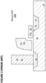
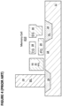
- Non-volatile memory cells are well known in the art. Examples of non-volatile memory cells known in the prior art are shown in Figures 1-6 .
- FIG. 1 depicts stacked-gate non-volatile memory cell 110.
- Each memory cell 110 includes source region (also referred to as source line terminal) 14 and drain region 16 formed in semiconductor substrate 12, with channel region 18 there between.
- Floating gate 20 is formed over and insulated from (and controls the conductivity of) channel region 18, and over a portion of each of the drain region 16 and the source region 14.
- Control gate terminal 22 (which here is coupled to a word line) is disposed over and insulated from floating gate 20.
- the floating gate 20 and control gate terminal 22 are insulated from each other and from the substrate 12 by a gate oxide.
- Bitline terminal 24 is coupled to drain region 16.
- Programming is performed using hot electron injection from channel 18 to floating gate 20 in the channel region next to the drain region 16.
- Erasing is performed using by Fowler-Nordheim electron tunneling from floating gate 20 to substrate 12.
- Reading is performed by placing positive read voltages on the drain region 16 and control gate terminal 22 (which turns on channel region 18). If the floating gate 20 is positively charged (i.e. erased of electrons), then channel region 18 under the floating gate 20 is turned on as well, and current will flow across the channel region 18, which is sensed as the erased or "1" state. If the floating gate 20 is negatively charged (i.e. programmed with electrons), then the channel region under the floating gate 20 is mostly or entirely turned off, and current will not flow (or there will be little flow) across the channel region 18, which is sensed as the programmed or "0" state.
- Table No. 1 depicts typical voltage ranges that can be applied to the terminals of memory cell 110 and substrate 12 for performing read, erase, and program operations: Table No. 1: Operation of Stacked-Gate Non-Volatile Memory Cell 110 of Figure 1 CG BL SL Substrate Read 1 0-5V 0.1 - 2V 0-2V 0V Read 2 0.5-2V 0-2V 2-0.1V 0V Erase -8 to -10V/0V FLT FLT 8-10V / 15-20V Program 8-12V 3-5 V/0 V 0V/3-5V 0V "Read 1" is a read mode in which the cell current is output on the bit line. "Read 2" is a read mode in which the cell current is output on source line terminal 14.
- the bit line terminal is set to VDD (typically 3-5 V) and the source line terminal is set to 0 V to inhibit programming of the cell, and the bit line terminal is set to 0 V and the source line terminal is set to VDD (typically 3-5 V) to program the cell.
- VDD typically 3-5 V
- FIG. 2 depicts split-gate non-volatile memory cell 210.
- Each memory cell 210 includes source region (source line terminal) 14 and drain region 16 formed in semiconductor substrate 12, with channel region 18 there between.
- Floating gate 20 is formed over and insulated from (and controls the conductivity of) a first portion of the channel region 18, and over a portion of the source region 14.
- Word line terminal 22 (which is typically coupled to a word line) has a first portion that is disposed over and insulated from (and controls the conductivity of) a second portion of the channel region 18, and a second portion that extends up and over the floating gate 20.
- the floating gate 20 and word line terminal 22 are insulated from the substrate 12 by a gate oxide.
- Bitline terminal 24 is coupled to drain region 16.
- Memory cell 210 is erased (where electrons are removed from the floating gate) by placing a high positive voltage on the word line terminal 22, which causes electrons on the floating gate 20 to tunnel through the intermediate insulation from the floating gate 20 to the word line terminal 22 via Fowler-Nordheim tunneling.
- Memory cell 210 is programmed (where electrons are placed on the floating gate) by placing a positive voltage on the word line terminal 22, and a positive voltage on the source region 14. Electron current will flow from the drain region 16 towards the source region 14 (source line terminal). The electrons will accelerate and become energized (heated) when they reach the gap between the word line terminal 22 and the floating gate 20. Some of the heated electrons will be injected through the gate oxide onto the floating gate 20 due to the attractive electrostatic force from the floating gate 20.
- Memory cell 210 is read by placing positive read voltages on the drain region 16 and word line terminal 22 (which turns on the portion of the channel region 18 under the word line terminal). If the floating gate 20 is positively charged (i.e. erased of electrons), then the portion of the channel region 18 under the floating gate 20 is turned on as well, and current will flow across the channel region 18, which is sensed as the erased or " 1" state. If the floating gate 20 is negatively charged (i.e. programmed with electrons), then the portion of the channel region under the floating gate 20 is mostly or entirely turned off, and current will not flow (or there will be little flow) across the channel region 18, which is sensed as the programmed or "0" state.
- Table No. 2 depicts typical voltage ranges that can be applied to the terminals of memory cell 210 for performing read, erase, and program operations: Table No. 2: Operation of Non-Volatile Memory Cell 210 of Figure 2 WL BL SL Read 1 0.5-3V 0.1-2V 0V Read 2 0.5-3V 0-2V 2-0.1V Erase ⁇ 11-13V 0V 0V Program 1-2V 1-3 ⁇ A 9-10V
- Read 1 is a read mode in which the cell current is output on the bit line.
- Read 2 is a read mode in which the cell current is output on source line terminal 14.
- Figure 3 depicts split-gate non-volatile memory cell 310.
- Memory cell 310 is similar to memory cell 210 of Figure 2 with the addition of control gate (CG) terminal 28.
- Control gate terminal 28 is biased at a high positive voltage, e.g., 10V, in programming, low or negative voltage in erase, e.g., 0v/-8V, low or mid-range voltage in read, e.g., 0v/2.5V.
- Other terminals are biased similarly to that of Figure 2 .
- FIG. 4 depicts split-gate non-volatile memory cell 410.
- Memory cell 410 comprises source region (source line terminal) 14, drain region 16, floating gate 20 over a first portion of channel region 18, a select gate 22 (typically coupled to a word line, WL) over a second portion of the channel region 18, a control gate 28 over the floating gate 20, and an erase gate 30 over the source region 14.
- all gates are non-floating gates except floating gate 20, meaning that they are electrically connected or connectable to a voltage source. Programming is performed by heated electrons from the channel region 18 injecting themselves onto the floating gate 20. Erasing is performed by electrons tunneling from the floating gate 20 to the erase gate 30.
- Table No. 3 depicts typical voltage ranges that can be applied to the terminals of memory cell 410 for performing read, erase, and program operations: Table No. 3: Operation of Non-Volatile Memory Cell 410 of Figure 4 WL/SG BL CG EG SL Read 1 0.5-2V 0.1-2V 0-2.6V 0-2.6V 0V Read 2 0.5-2V 0-2V 0-2.6V 0-2.6V 2-0.1V Erase -0.5V/0V 0V 0V/-8V 8-12V 0V Program 1V 1 ⁇ A 8-11V 4.5-9V 4.5-5V "Read 1" is a read mode in which the cell current is output on the bit line.
- “Read 2" is a read mode in which the cell current is output on the source line terminal.
- Figure 5 depicts split-gate non-volatile memory cell 510.
- Memory cell 510 is similar to memory cell 410 of Figure 4 except that memory cell 510 does not contain an erase gate EG terminal. Programming is performed by heated electrons from the channel region 18 injecting themselves onto the floating gate 20. An erase is performed by biasing the substrate 12 to a high voltage and biasing the control gate CG terminal 28 to a low or negative voltage such that electrons tunnel from the floating gate 20 to the channel region 18. Alternatively, an erase is performed by biasing word line terminal 22 to a positive voltage and biasing control gate terminal 28 to a negative voltage such that electrons tunnel from the floating gate 20 to the word line terminal 22. Programming and reading is similar to that of Figure 4 .
- Figure 6 depicts split-gate non-volatile memory cell 610.
- Memory cell 610 is identical to the memory cell 410 of Figure 4 except that memory cell 610 does not have a separate control gate terminal.
- the erase operation (whereby erasing occurs through use of the erase gate terminal) and read operation are similar to that of the Figure 4 except there is no control gate bias applied.
- the programming operation also is done without the control gate bias, and as a result, a higher voltage must be applied on the source line terminal 14 during a program operation to compensate for a lack of control gate bias.
- Table No. 4 depicts typical voltage ranges that can be applied to the terminals of memory cell 610 for performing read, erase, and program operations: Table No. 4: Operation of Non-Volatile Memory Cell 610 of Figure 6 WL/SG BL EG SL Read 1 0.5-2.2V 0.1-2V 0-2.6V 0V Read 2 0.5-2.2V 0-2V 0-2.6V 2-0.1V Erase -0.5V/0V 0V 11.5V 0V Program 1V 2-3 ⁇ A 4.5V 7-9V "Read 1" is a read mode in which the cell current is output on the bit line. "Read 2" is a read mode in which the cell current is output on the source line terminal.
- Memory cells of the types shown in Figures 1-6 typically are arranged into rows and columns to form an array. Erase operations are performed on entire rows or pairs of rows at one time, since each word lines controls a row of memory cells and is coupled to word line terminal 22 of each cell in that row, and erase gate lines (when present) are shared by pairs of rows of memory cells and are coupled to erase gate terminals 30 of each cell in those pairs of rows.
- Source lines typically are coupled to source line terminals 14 of one row of memory cells or two adjacent rows of memory cells.
- Bitlines typically are coupled to bit line terminals 24 of one column of memory cells 24.
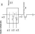
- Memory system 700 comprises memory cell 710, word line 722, control gate line 726, erase gate line 728, bit line 720, and source line 714.
- Memory cell 710 can be any of the types shown in Figures 1-6 , namely, memory cell 110, memory cell 210, memory cell 310, memory cell 410, memory cell 510, memory cell 610, or another type of memory cell.
- Source line 714 is coupled to pull down transistor 730, which here comprises a single NMOS transistor. When the gate of pull down transistor 730 is activated, source line 714 is pulled down to ground.
- each source line 714 may require more than one pull down circuit depending on the capacitance of the source line 714.
- the pull down transistors 714 require operating voltages of around 0-1.2 V for low voltage operations and 4-5-11.5 V for high voltage operations, as shown in Tables 1-4. This means that pull down transistor 730 needs one or both of a high voltage transistor type (e.g., 11.5V transistor) or an IO transistor type (e.g., 2.5V or 3V transistor), which takes up die space and increases the overall cost and complexity of the system.
- a high voltage transistor type e.g., 11.5V transistor
- an IO transistor type e.g., 2.5V or 3V transistor
- both types In the situation where both types are present, they typically will be connected to ground on one end and to a multiplexor on the other end, where the multiplexor connects one of the transistors to the source line in response to a control signal.
- the pull down transistors can incur overstress and breakdown when memory cell 710 is programmed.
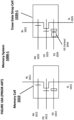
- flash memory system 800 comprises exemplary memory cell 710 and exemplary dummy memory cell 810.
- Dummy memory cell 810 is of the same construction as memory cell 710 except that dummy memory cell 810 is not used to store data.
- Source line 714 of memory cell 710 is coupled to source line 814 of dummy memory cell 810, as would typically be the case if memory cell 710 and dummy memory cell 810 are in the same row within an array.
- Word line 722 is coupled to word line 822, and bit line 720 is shared among memory cells 800 of the column.
- memory cell 710 and dummy memory cell 810 follow the design of memory cell 410 in Figure 4 . It will be understood that memory cell 710 and dummy memory cell 810 also can follow the design of memory cell 310 in Figure 3 or memory cell 510 in Figure 5 (in which case erase gates 728 and 828 will not be present), of memory cell 610 in Figure 6 (in which case control gates 726 and 826 will not be present), or of memory cell 110 in Figure 1 or memory cell 210 in Figure 2 (in which case erase gates 728 and 828 and control gate 726 and 826 will not be present).
- source line 814 is coupled to ground through the dummy memory cell 810 and dummy bitline 820, which is switchably coupled to ground, which results in source line 714 and source line 814, anything else that is electrically connected to bit line 820, being pulled to ground.
- Dummy memory cells 810 are required to be erased before a read operation.
- dummy bitline 820 When the memory cell 710 is in program mode, dummy bitline 820 is switchably coupled to an inhibit voltage such as VDD. This will place dummy memory cell 810 in a program inhibit mode which maintains dummy memory cell 810 in an erased state. There can be a plurality of dummy memory cells 810 for each memory cell 710 to strengthen the pull down of the source line 714 to ground.
- Figure 9 depicts flash memory system 900, which comprises exemplary memory cells 920 and exemplary dummy memory cell circuit 910.
- Dummy memory cell circuit 910 comprises a plurality of dummy memory cells coupled to one another.
- source line 930 (also labeled SL0) and source line 940 (also labeled SL1) from memory cells 920 are coupled to source line terminals of dummy memory cell circuit 910.
- source line 930 SL0 and source line 940 SL1 are connected together.
- the source lines for an entire sector or sectors of memory cells 920 can be coupled together to a source line of dummy memory cell circuit 910 comprising dummy memory cells from the same rows of cells that are part of the sector or sectors.
- dummy memory cell circuit 910 When memory cells 920 are in read mode or erase mode, dummy memory cell circuit 910 will be coupled to ground through the dummy bitlines. The dummy memory cells are required to be erased before a read operation. The erased dummy memory cells, when coupled to ground through the dummy bitlines will pull source lines 930 and 940 to ground.
- the dummy bitlines of dummy memory cell circuit 910 When memory cells 920 are in program mode, the dummy bitlines of dummy memory cell circuit 910 will be coupled to an inhibit voltage such as VDD. This will place the dummy memory cells of dummy memory cell circuit 910 in a program inhibit mode, which maintains the dummy memory cells in an erased state.
- VDD inhibit voltage
- word line 950 also labeled WL_rdcellpdwn, which is separate from wordlines of the memory cell 920
- control gate 960 also labeled CG_rdcellpdwn, which is separate from control gates of the memory cell 920
- word line 950 also labeled WL_rdcellpdwn, which is separate from wordlines of the memory cell 920
- control gate 960 also labeled CG_rdcellpdwn, which is separate from control gates of the memory cell 920
- Figures 8 and 9 require additional die space for the dummy memory cells of the dummy memory cell circuit. This increases the size, complexity, and manufacturing cost of the die.
- FIGS 10A , 10B , 10C , and 10D depict prior art memory systems 1000-1, 1000-2, 1000-3, and 1000-4, respectively, which comprise exemplary memory cell 1010 and exemplary strap cell 1020, i.e. exemplary strap cell 1020-1, 1020-2, 1020-3 and 1020-4, respectively.
- Strap cell 1020 is part of a strap row or a strap column that typically is present in the array as an area in which physically connections can be made between one or more of erase gate lines, source lines, control gate lines, and word lines and another structure outside of the array (such as a driver, low voltage decoder, or high voltage decoder). Strap cell 1020 contains some, but not always all, of the same components as memory cell 1010.
- memory cell 1010 comprises first bit line terminal 1011, first word line terminal 1012, first control gate terminal 1013, first erase gate terminal 1014, and first source line terminal 1015, as would be the case if memory cell 1010 follows the design of memory cell 410 in Figure 4 .
- Strap cell 1020 could be one of four different types of strap cells: erase gate strap cell 1020-1 (shown in Figure 10A ), source line strap cell 1020-2 (shown in Figure 10B ), control gate strap cell 1020-3 (shown in Figure 10C ), and word line strap cell 1020-4 (shown in Figure 10D ).
- strap cell 1020 can be erase gate strap cell 1020-1, comprising second bit line terminal 1021, second word line terminal 1022, second control gate terminal 1023, second erase gate terminal 1024, second source line terminal 1025, and erase gate contact 1034, where erase gate contact 1034 connects second erase gate terminal 1024 to a structure (such as a low voltage or high voltage decoder) outside of the array containing memory cell 1010 and strap cell 1020-1 that drives the erase gate line 1104 connected to second erase gate terminal 1024 as needed during program, erase, and read operations. Second erase gate terminal 1024 is further connected to erase gate line 1104 since it is in the same row as memory cell 1010.
- Memory cell 1010 comprises a first word line terminal 1012, a first control gate terminal 1013, an first erase gate terminal 1014, a first source line terminal 1015 and a first bit line terminal 1011.
- Figure 11A depicts an example of an array containing erase gate strap cell 1020-1.
- Array 1100-1 comprises bit lines 1101, word lines 1102a and 1102b, control gate lines 1103a and 1103b, erase gate line 1104, and source line 1105.
- Source line 1105 is located underneath erase gate line 1104, and therefore from this view would appear to be the same line even though they are separate in the three-dimensional space.
- Exemplary memory cell 1010 is depicted.
- the word line terminal (such as first word line terminal 1012 in Figure 10 ) of cell 1010 is coupled to word line 1102a
- the control gate terminal of memory cell 1010 (such as first control gate terminal 1013 in Figure 10 ) is coupled to control gate line 1103a
- the erase gate terminal (such as first erase gate terminal 1014 in Figure 10 ) of cell 1010 is coupled to erase gate line 1104
- the source line terminal such as first source line terminal 1015 in Figure 10 ) of memory cell 1010 is coupled to source line 1105.
- Bit lines 1101 are coupled to structures outside of array 1100 through bit line contacts 1106 (which are located at either end of each bit line).
- Array 1100 also comprises erase gate strap 1110, which comprises exemplary erase gate strap cell 1020-1.
- Erase gate strap 1110 is coupled to erase gate line 1104, since it is in the same row, and thus erase gate line 1104 and erase gate terminal 1014 of memory cell 1010 are coupled to erase gate contact 1034.
- Strap cell 1020-1 and erase gate strap 1110 are not connected to any bit line contacts and therefore are not connected to its corresponding bit line to a structure outside of array 1100. As a result, strap cell 1020-1 and erase gate strap 1110 have no pull down function in the prior art.
- strap cell 1020 can be source line strap cell 1020-2.
- Source line strap cell 1020-2 comprises second bit line terminal 1021, second word line terminal 1022, second control gate terminal 1023, second source line terminal 1025, and source line contact 1035 and does not comprise an erase gate terminal (to provide room for source line contact 1035), where source line contact 1035 connects to a structure (such as a low voltage or high voltage decoder) outside of the array containing memory cell 1010 and strap cell 1020-2 that drives the source line connected to second source line terminal 1025 as needed during program, erase, and read operations.
- Memory cell 1010 comprises a first word line terminal 1012, a first control gate terminal 1013, a first erase gate terminal 1014, a first source line terminal 1015 and a first bit line terminal 1011.
- Figure 11B depicts an example of an array containing source line strap cell 1020-2.
- Array 1100-2-2 is similar to array 1100-1 of Figure 11A , except that erase gate strap 1110 is replaced with source line strap 1120, which comprises exemplary source line strap cell 1020-2.
- Source line strap 1120 is coupled to source line 1105, since it is in the same row, and thus source line 1105 and source line terminal 1015 of memory cell 1010 are coupled to source line contact 1035.
- Source line strap cell 1020-2 and source line strap 1120 are not connected to any bit line contacts and therefore are not connected via their associated bit line to a structure outside of array 1100-2. As a result, source line strap cell 1020-2 and source line strap 1120 performs no pull down function in the prior art.
- strap cell 1020 can be control gate strap cell 1020-3.
- Control gate strap cell 1020-3 comprises second bit line terminal 1021, second word line terminal 1022, second control gate terminal 1023, second source line terminal 1025, control gate contact 1033, and source line contact 1035 and does not comprise an erase gate terminal (to provide room for source line contact 1035), where control gate contact 1033 and source line contact 1035 connect to structures (such as a low voltage or high voltage decoders) outside of the array containing memory cell 1010 and strap cell 1020-3 that drives the control gate line 1103a and source line 1105 connected to second control gate terminal 1023 and source line terminal 1025, respectively, as needed during program, erase, and read operations.
- Memory cell 1010 comprises a first word line terminal 1012, a first control gate terminal 1013, a first erase gate terminal 1014, a first source line terminal 1015 and a first bit line terminal 1011.
- Figure 11C depicts an example of an array containing control gate line strap cell 1130.
- Array 1100-3 is similar to array 1100-1 and 1100-2 in Figures 11A and 11B , respectively, except that the except that erase gate strap 1110 or source line strap 1120, respectively, are replaced with control gate line strap 1130, which comprises exemplary control gate strap cell 1020-3.
- Control gate line strap 1130 particularly control gate strap cells 1020-3 (one of which is called out), are respectively coupled to control gate lines 1103a and 1103b, since they are in the same row, and thus control gate lines 1103a, 110b, and control gate terminals 1013 of memory cells 1010, respectively, are coupled to control gate line contacts 1033a and 1033b, respectively.
- Source line 1105 is coupled to second source line terminal 1025, since they are in the same row, and thus source line 1105 is coupled to source line contact 1035.
- Control gate line strap cell 1020-3 and control gate line strap 1130 are not connected to any bit line contacts and therefore are not connected via their associated bit line to a structure outside of array 1100-3. As a result, control gate line strap cell 1020-3 and control gate line strap 1130 perform no pull down function in the prior art.
- strap cell 1020 can be word line strap cell 1020-4.
- Word line strap cell 1020-4 comprises second bit line terminal 1021, second word line terminal 1022, second control gate terminal 1023, second source line terminal 1025, word line contact 1032, and source line contact 1035 and does not comprise an erase gate terminal (to provide room for source line contact 1035), where word line contact 1032 and source line contact 1035 connect to structures (such as a low voltage or high voltage decoders) outside of the array containing memory cell 1010 and strap cell 1020-4 that drive the word line and source line connected to word line contact 1032 and source line contact 1035, respectively, as needed during program, erase, and read operations.
- Memory cell 1010 comprises a first word line terminal 1012, a first control gate terminal 1013, a first erase gate terminal 1014, a first source line terminal 1015 and a first bit line terminal 1011.
- Figure 11D depicts an example of an array containing word line strap cell 1020-4.
- Array 1100-4 is similar to arrays 1100-1, 1100-2, and 1100-3 of Figures 11A , 11B , and 11C , respectively, except that the except that erase gate strap 1110, source line strap 1120 or control gate line strap 1130, respectively, are replaced with word line strap 1140, which comprises exemplary word line strap cell 1020-4.
- Word line strap 1140 are coupled to word lines 1102a and 1102b, since they are in the same row, respectively, and thus word lines 1102a and 1102b and word line terminals 1012 of memory cells 1010, are coupled to word line contacts 1032a and 1032b, respectively.
- Source line 1105 is coupled to second source line terminal 1025, since they are in the same row, and thus source line 1105 is coupled to source line contact 1035.
- Strap cell 1020-4 and word line strap 1140 are not connected to any bit line contacts and therefore are not connected via their associated bit line to a structure outside of array 1100-4. Word line strap cell 1020-4 and word line strap 1140 therefore perform no pull down function in the prior art.
- first source line terminal 1015 of memory cell 1010 is coupled to the same source line as second source line terminal 1025 of strap cell 1020
- first word line terminal 1012 of memory cell 1010 is coupled to the same word line as second word line terminal 1022 of strap cell 1020
- first control gate terminal 1013 of memory cell 1010 is coupled to the same control gate line as second control gate terminal 1023 of strap cell 1020
- first erase gate terminal 1014 of memory cell 1010 is coupled to the same erase gate line as second erase gate terminal 1024 (if present) of strap cell 1020.
- memory cell 1010 and strap cell 1020 follow the design of memory cell 410 in Figure 4 , with the exceptions described above for strap cells 1020-2, 1020-3, and 1030-4.
- Memory cell 1010 and strap cell 1020 also can follow the design of memory cell 310 in Figure 3 or memory cell 510 in Figure 5 (in which case first and second erase gate terminals 1014 and 1024 will not be present), of memory cell 610 in Figure 6 (in which case first and second control gate terminals 1013 and 1023 will not be present), or of memory cell 110 in Figure 1 or memory cell 210 in Figure 2 (in which case first and second erase gate terminals 1014 and 1024 and first and second control gate terminals 1013 and 1023 will not be present).
- a strap cell is a cell, not used for storing data, comprising at least one of an erase gate contact, a control gate contact, a source line contact and a word line contact which connect to a structure (such as a low voltage decoder or high voltage decoder) outside of the array containing the memory cells.
- the respective erase gate contact, control gate contact, source line contact and word line contact are vertical contacts which connect to a metal line, which metal line are connected to the structure (such as a low voltage decoder or high voltage decoder) outside of the array containing the memory cells.
- a flash memory device utilizes existing strap cells in the array in source line pull down circuits.
- a memory system comprises a memory cell comprising a first bit line terminal and a first source line terminal; a strap cell comprising a second bit line terminal and a second source line terminal; a source line coupled to the first source line terminal and the second source line terminal; and a pull down circuit that selectively couples the second bitline terminal to ground when the memory cell is being read or erased and to a voltage source when the memory cell is being programmed.
- the memory cell comprises a first word line terminal and the strap cell comprises a second word line terminal. In certain embodiments, the memory cell comprises a first control gate terminal and the strap cell comprises a second control gate terminal. In certain embodiments, the memory cell comprises a first erase gate terminal and the strap cell comprises a second erase gate terminal.
- the strap cell is a source line strap cell, wherein the second source line terminal is connected to a source line contact.
- the strap cell is a word line strap cell, wherein the second word line terminal is connected to a word line contact.
- the strap cell is a control gate strap cell, wherein the second control line terminal is connected to a control gate contact.
- the strap cell is an erase gate strap cell wherein the second erase gate terminal is connected to an erase gate contact.
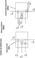
- FIG 12 depicts an embodiment with a strap cell used as a pull down circuit for a source line.
- Memory system 1200 comprises memory cell 1010, which comprises the same components described previously for memory cell 1010 with respect to Figures 10A-10D , in particular memory cell 1010 comprises a first word line terminal 1012, a first control gate terminal 1013, a first erase gate terminal 1014, a first source line terminal 1015 and a first bit line terminal 1011.
- Memory system 1200 also comprises strap cell 1020, which can be any of strap cells 1020-1, 1020-2, 1020-3, and 1020-4 described previously with respect to Figures 10A-10D and 11A-11D .
- second bit line terminal 1021 of strap cell 1020 is connected to pull down circuit contact 1201 (which can comprise, for example, a via between layers), which in turn connects outside of the memory array to pull down circuit 1210.
- Pull down circuit 1210 comprises switch 1211 that, in response to a control signal, will be selectively connected to ground or a voltage source such as VDD.
- first source line terminal 1015 is coupled to source line 1105, which is coupled to strap cell 1020 and pull down circuit 1210 to ground.
- first source line terminal 1015, source line 1105, and second source line terminal 1025 will be pulled down to ground through strap cell 1020.
- more than one strap cell 1020 can be coupled to first source line terminal 1015 to strengthen the pull down of the first source line terminal 1015 and source line 1105 to ground so as to cause first source line terminal 1015 and source line 1105 to pull to ground faster.
- second bit line terminal 1021 is coupled to an inhibit voltage source such as VDD through switch 1211 in pull down circuit 1210. This will place strap cell 1020 in a program inhibit mode, which maintains strap cell 1020 in an erased state, even while memory cell 1010 is programmed.
- Strap cell 1020 is produced in a neutral state, in which it conducts current (equivalent to an erased state). When memory cell 1010 is erased, strap cell 1020 similarly experiences erase potentials, and thus remains in the erased state at all times, or optionally is not erased and is kept in a neutral state, in which current flows through strap cell 1020, since when memory cell 1010 is programmed, strap cell 1020 experiences inhibit program potentials responsive to pull down circuit 1210.
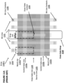
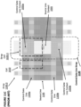
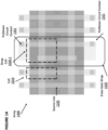
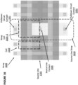
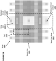
- Figures 13-18 depict exemplary layouts of embodiments utilizing the four types of strap cells (erase gate strap cell 1020-1, source line strap cell 1020-2, control gate strap cell 1020-3, and word line strap cell 1020-4) for strap cell 1020, respectively.
- Figure 13 depicts array 1300, which is similar to array 1100-1, except that the bit line terminal 1021 (not shown, but seen in Figure 10A - 10D ) in erase gate strap 1310 is connected to pull down circuit contacts 1201 on both ends of the bit line, which in turn connects to a switchable contact of respective pull down circuits 1210 (not shown here, but shown in Figure 12 ).
- Cell 1010 and erase gate strap cell 1020-1 share source line 1105, and source line 1105 is pulled down to ground through pull down circuit contacts 1201 and respective pull down circuits 1210 during a read mode or an erase mode, and is pulled to VDD through pull down circuit contacts 1201 responsive to pull down circuits 1210 during a program mode, as discussed previously with reference to Figure 12 .
- Figure 14 depicts array 1400, which is similar to array 1300, except that erase gate strap 1410 is wider than erase gate strap 1310, and erase gate strap cell 1020-2 is wider in array 1400 than in array 1300, in this example, by a factor of 2x. This increases the pull down capability.
- Cell 1010 and erase gate strap cell 1020-2 share source line 1105, and source line 1105 is pulled down to ground through pull down circuit contacts 1201 responsive to pull down circuits 1210 during a read mode or an erase mode, and is pulled to VDD through pull down circuit contacts 1201 responsive to pull down circuits 1210 during a program mode, as discussed previously with reference to Figure 12 .
- Figure 15 depicts array 1500, which is similar to array 1400 of Figure 14 , except that (1) erase gate strap 1410 has been replaced with erase gate strap 1510, which comprises two columns of erase gate strap cells, each similar in size to a column of memory cells, (2) there are two erase gate strap cells 1020-2 instead of one, and (3) erase gate strap 1510 has four pull down circuit contacts 1201 each connected to a respective bit line terminal, instead of two .
- Array 1500 might be easier to manufacture than array 1400 due to the relative uniformity among the columns of normal cells and the two columns of erase gate strap cells.
- Figure 16 depicts array 1600, which comprises source line strap 1610.
- Array 1600 is similar to array 1100-2 of Figures 11B , except that he bit line terminal in source line strap 1610 is connected to pull down circuit contacts 1201 on both ends of the bit line, which in turn connects to a switchable contact of respective pull down circuits 1210 (not shown here, but shown in Figure 12 ).
- Cell 1010 and source line strap cell 1020-2 share source line 1105, and shared source line 1105 is pulled down to ground through pull down circuit contact 1201 responsive to pull down circuits 1210 during a read or erase mode, and is pulled to VDD through pull down circuit contacts 1201 responsive to pull down circuits 1210 during a program mode, as discussed previously with reference to Figure 12 .
- Figure 17 depicts array 1700, which comprises control gate line strap 1710.
- Array 1700 is similar to array 1100-3 of Figure 11C , except that the bit line terminal in control gate line strap 1710 is connected to pull down circuit contacts 1201 on both ends of the bit line, which in turn connect to switchable contacts of respective pull down circuits 1210 (not shown here, but shown in Figure 12 ).
- Cell 1010 and control gate strap cell 1020-3 share source line 1105, and source line 1105 is pulled down to ground through pull down circuit contacts 1201 responsive to pull down circuit 1210 during a read mode or erase mode, and is pulled to VDD through pull down circuit contacts 1201 responsive to pull down circuits 1210 during a program mode, as discussed previously with reference to Figure 12 .
- Figure 18 depicts array 1800, which comprises word line strap 1810.
- Array 1800 is similar to array 1100-4 of Figure 11D , except that the bit line terminals in word line strap 1810 are respectively connected to pull down circuit contacts 1201 on both ends of the bit line, which in turn connects to the switchable contacts of respective pull down circuits 1210 (not shown here, but shown in Figure 12 ).
- Cell 1010 and word line strap cell 1020-4 share source line 1105, and source line 1105 is pulled down to ground through pull down circuit contacts 1201 responsive to pull down circuits 1210 during a read mode or erase mode, and is pulled to VDD through pull down circuit contacts 1201 responsive to pull down circuits 1210 during a program mode, as discussed previously with reference to Figure 12 .
- the term “adjacent” includes “directly adjacent” (no intermediate materials, elements or space disposed therebetween) and “indirectly adjacent” (intermediate materials, elements or space disposed there between)
- “coupled” includes “directly coupled to” (no intermediate materials or elements therebetween that electrically connect the elements together) and “indirectly coupled to” (intermediate materials or elements therebetween that electrically connect the elements together).
- forming an element "over a substrate” can include forming the element directly on the substrate with no intermediate materials/elements therebetween, as well as forming the element indirectly on the substrate with one or more intermediate materials/elements there between.
Landscapes
- Engineering & Computer Science (AREA)
- Microelectronics & Electronic Packaging (AREA)
- Non-Volatile Memory (AREA)
- Read Only Memory (AREA)
Description
- This application claims the benefit of
Chinese Patent Application No. 202010304167.2, filed on April 17, 2020 U.S. Patent Application No. 17/074,103 filed on October 19, 2020 . - The present invention relates to a non-volatile memory device that utilizes existing strap cells in the array in source line pull down circuits.
-
EP 3347899 A1 discloses that the present invention relates to a flash memory device that uses dummy memory cells as source line pull down circuits. -
US 20180204627 A1 discloses that the present invention relates to a flash memory cell with only four terminals and decoder circuitry for operating an array of such flash memory cells. The invention allows for fewer terminals for each flash memory cell compared to the prior art, which results in a simplification of the decoder circuitry and overall die space required per flash memory cells. The invention also provides for the use of high voltages on one or more of the four terminals to allow for read, erase, and programming operations despite the lower number of terminals compared to prior art flash memory cells. -
US 20100226181 A1 discloses that a non-volatile memory device comprises an array of non-volatile memory cells arranged in a plurality of rows and columns. Each memory cell has a bit terminal for connection to a bit line, a high voltage terminal for connection to a high voltage source, and a low voltage terminal for connection to a low voltage source. The array has a first side adjacent to a first column of memory cells, and a second side opposite the first side, a third side adjacent to a first row of memory cells, and a fourth side opposite the third side. The memory device further comprises a plurality of columns of reference memory cells embedded in the memory array, with a plurality of reference cells in each row of the array of non-volatile memory cells, substantially evenly spaced apart from one another. Each of the reference memory cells is substantially the same as the non-volatile memory cells, and has a bit terminal for connection to a bit line, a high voltage terminal for connection to a high voltage source and a low voltage terminal for connection to a low voltage source. A high voltage decoder is positioned on the first side, and has a plurality of high voltage lines, with each high voltage line connected to the high voltage terminal of the memory cells and reference cells in the same row. A low voltage row decoder is positioned on the second side, and has a plurality of low voltage lines, with each low voltage line connected to the low voltage terminal of the memory cells and reference cells in the same row. A plurality of sense amplifiers are positioned on the third side, with each sense amplifier connected to the bit terminal of one column of non-volatile memory cells and to the bit terminal of a column of reference memory cells. This invention also includes N-of-M selective reference scheme, distributed source line pull down, source line resistance strap compensation, replica-data-pattern current consumption, data current compensation, and bit line voltage error compensation. -
US 20200105775 A1 discloses that various embodiments of the present application are directed towards an integrated memory chip comprising a memory array with a strap-cell architecture that reduces the number of distinct strap-cell types and that reduces strap-line density. In some embodiments, the memory array is limited to three distinct types of strap cells: a source line/erase gate (SLEG) strap cell; a control gate/word line (CGWL) strap cell; and a word-line strap cell. The small number of distinct strap-cell types simplifies design of the memory array and further simplifies design of a corresponding interconnect structure. Further, in some embodiments, the three distinct strap-cell types electrically couple word lines, erase gates, and control gates to corresponding strap lines in different metallization layers of an interconnect structure. By spreading the strap lines amongst different metallization layers, strap-line density is reduced. -
US 20100008141 A1 discloses a semiconductor device with multiple strap-contact configurations for a memory cell array. An array with memory cells interconnected with bitlines, control-gate lines, erase gate lines, common-source lines, and word-lines is provided. In one aspect of an illustrative embodiment, a strap-contact corridor is spaced at n bit-line intervals (n>1) across the array. The strap-contact corridor comprises strap-contact cells, which provide electrical interconnection between control-gate lines, erase gate lines, common-source lines, and word-lines and their respective straps. - The present invention is defined in the independent claims. Preferred embodiments are defined in the dependent claims.
- Non-volatile memory cells are well known in the art. Examples of non-volatile memory cells known in the prior art are shown in
Figures 1-6 . -
Figure 1 depicts stacked-gate non-volatilememory cell 110. Eachmemory cell 110 includes source region (also referred to as source line terminal) 14 anddrain region 16 formed insemiconductor substrate 12, withchannel region 18 there between. Floatinggate 20 is formed over and insulated from (and controls the conductivity of)channel region 18, and over a portion of each of thedrain region 16 and thesource region 14. Control gate terminal 22 (which here is coupled to a word line) is disposed over and insulated fromfloating gate 20. Thefloating gate 20 andcontrol gate terminal 22 are insulated from each other and from thesubstrate 12 by a gate oxide.Bitline terminal 24 is coupled todrain region 16. - Programming is performed using hot electron injection from
channel 18 to floatinggate 20 in the channel region next to thedrain region 16. - Erasing is performed using by Fowler-Nordheim electron tunneling from
floating gate 20 tosubstrate 12. - Reading is performed by placing positive read voltages on the
drain region 16 and control gate terminal 22 (which turns on channel region 18). If thefloating gate 20 is positively charged (i.e. erased of electrons), thenchannel region 18 under thefloating gate 20 is turned on as well, and current will flow across thechannel region 18, which is sensed as the erased or "1" state. If thefloating gate 20 is negatively charged (i.e. programmed with electrons), then the channel region under thefloating gate 20 is mostly or entirely turned off, and current will not flow (or there will be little flow) across thechannel region 18, which is sensed as the programmed or "0" state. - Table No. 1 depicts typical voltage ranges that can be applied to the terminals of
memory cell 110 andsubstrate 12 for performing read, erase, and program operations:Table No. 1: Operation of Stacked-Gate Non-Volatile Memory Cell 110 of Figure 1CG BL SL Substrate Read 1 0-5V 0.1 - 2V 0-2V 0V Read 2 0.5-2V 0-2V 2-0.1V 0V Erase -8 to -10V/0V FLT FLT 8-10V / 15-20V Program 8-12V 3-5 V/0 V 0V/3-5V 0V "Read 1" is a read mode in which the cell current is output on the bit line. "Read 2" is a read mode in which the cell current is output on source line terminal 14. In the program mode, the bit line terminal is set to VDD (typically 3-5 V) and the source line terminal is set to 0 V to inhibit programming of the cell, and the bit line terminal is set to 0 V and the source line terminal is set to VDD (typically 3-5 V) to program the cell. -
Figure 2 depicts split-gate non-volatilememory cell 210. Eachmemory cell 210 includes source region (source line terminal) 14 anddrain region 16 formed insemiconductor substrate 12, withchannel region 18 there between. Floatinggate 20 is formed over and insulated from (and controls the conductivity of) a first portion of thechannel region 18, and over a portion of thesource region 14. Word line terminal 22 (which is typically coupled to a word line) has a first portion that is disposed over and insulated from (and controls the conductivity of) a second portion of thechannel region 18, and a second portion that extends up and over thefloating gate 20. Thefloating gate 20 andword line terminal 22 are insulated from thesubstrate 12 by a gate oxide.Bitline terminal 24 is coupled todrain region 16. -
Memory cell 210 is erased (where electrons are removed from the floating gate) by placing a high positive voltage on theword line terminal 22, which causes electrons on thefloating gate 20 to tunnel through the intermediate insulation from thefloating gate 20 to theword line terminal 22 via Fowler-Nordheim tunneling. -
Memory cell 210 is programmed (where electrons are placed on the floating gate) by placing a positive voltage on theword line terminal 22, and a positive voltage on thesource region 14. Electron current will flow from thedrain region 16 towards the source region 14 (source line terminal). The electrons will accelerate and become energized (heated) when they reach the gap between theword line terminal 22 and thefloating gate 20. Some of the heated electrons will be injected through the gate oxide onto thefloating gate 20 due to the attractive electrostatic force from thefloating gate 20. -
Memory cell 210 is read by placing positive read voltages on thedrain region 16 and word line terminal 22 (which turns on the portion of thechannel region 18 under the word line terminal). If thefloating gate 20 is positively charged (i.e. erased of electrons), then the portion of thechannel region 18 under thefloating gate 20 is turned on as well, and current will flow across thechannel region 18, which is sensed as the erased or " 1" state. If thefloating gate 20 is negatively charged (i.e. programmed with electrons), then the portion of the channel region under thefloating gate 20 is mostly or entirely turned off, and current will not flow (or there will be little flow) across thechannel region 18, which is sensed as the programmed or "0" state. - Table No. 2 depicts typical voltage ranges that can be applied to the terminals of
memory cell 210 for performing read, erase, and program operations:Table No. 2: Operation of Non-Volatile Memory Cell 210 of Figure 2WL BL SL Read 1 0.5-3V 0.1-2V 0V Read 2 0.5-3V 0-2V 2-0.1V Erase ~11-13V 0V 0V Program 1-2V 1-3µA 9-10V "Read 1" is a read mode in which the cell current is output on the bit line. "Read 2" is a read mode in which the cell current is output on source line terminal 14. -
Figure 3 depicts split-gatenon-volatile memory cell 310.Memory cell 310 is similar tomemory cell 210 ofFigure 2 with the addition of control gate (CG)terminal 28.Control gate terminal 28 is biased at a high positive voltage, e.g., 10V, in programming, low or negative voltage in erase, e.g., 0v/-8V, low or mid-range voltage in read, e.g., 0v/2.5V. Other terminals are biased similarly to that ofFigure 2 . -
Figure 4 depicts split-gate non-volatilememory cell 410.Memory cell 410 comprises source region (source line terminal) 14,drain region 16, floatinggate 20 over a first portion ofchannel region 18, a select gate 22 (typically coupled to a word line, WL) over a second portion of thechannel region 18, acontrol gate 28 over the floatinggate 20, and an erasegate 30 over thesource region 14. Here, all gates are non-floating gates except floatinggate 20, meaning that they are electrically connected or connectable to a voltage source. Programming is performed by heated electrons from thechannel region 18 injecting themselves onto the floatinggate 20. Erasing is performed by electrons tunneling from the floatinggate 20 to the erasegate 30. - Table No. 3 depicts typical voltage ranges that can be applied to the terminals of
memory cell 410 for performing read, erase, and program operations:Table No. 3: Operation of Non-Volatile Memory Cell 410 of Figure 4WL/SG BL CG EG SL Read 1 0.5-2V 0.1-2V 0-2.6V 0-2.6V 0V Read 2 0.5-2V 0-2V 0-2.6V 0-2.6V 2-0.1V Erase -0.5V/0V 0V 0V/-8V 8-12V 0V Program 1V 1µA 8-11V 4.5-9V 4.5-5V " Read 1" is a read mode in which the cell current is output on the bit line. "Read 2" is a read mode in which the cell current is output on the source line terminal. -
Figure 5 depicts split-gatenon-volatile memory cell 510.Memory cell 510 is similar tomemory cell 410 ofFigure 4 except thatmemory cell 510 does not contain an erase gate EG terminal. Programming is performed by heated electrons from thechannel region 18 injecting themselves onto the floatinggate 20. An erase is performed by biasing thesubstrate 12 to a high voltage and biasing the controlgate CG terminal 28 to a low or negative voltage such that electrons tunnel from the floatinggate 20 to thechannel region 18. Alternatively, an erase is performed by biasingword line terminal 22 to a positive voltage and biasingcontrol gate terminal 28 to a negative voltage such that electrons tunnel from the floatinggate 20 to theword line terminal 22. Programming and reading is similar to that ofFigure 4 . -
Figure 6 depicts split-gatenon-volatile memory cell 610.Memory cell 610 is identical to thememory cell 410 ofFigure 4 except thatmemory cell 610 does not have a separate control gate terminal. The erase operation (whereby erasing occurs through use of the erase gate terminal) and read operation are similar to that of theFigure 4 except there is no control gate bias applied. The programming operation also is done without the control gate bias, and as a result, a higher voltage must be applied on thesource line terminal 14 during a program operation to compensate for a lack of control gate bias. - Table No. 4 depicts typical voltage ranges that can be applied to the terminals of
memory cell 610 for performing read, erase, and program operations:Table No. 4: Operation of Non-Volatile Memory Cell 610 of Figure 6WL/SG BL EG SL Read 1 0.5-2.2V 0.1-2V 0-2.6V 0V Read 2 0.5-2.2V 0-2V 0-2.6V 2-0.1V Erase -0.5V/0V 0V 11.5V 0V Program 1V 2-3µA 4.5V 7-9V " Read 1" is a read mode in which the cell current is output on the bit line. "Read 2" is a read mode in which the cell current is output on the source line terminal. - Memory cells of the types shown in
Figures 1-6 typically are arranged into rows and columns to form an array. Erase operations are performed on entire rows or pairs of rows at one time, since each word lines controls a row of memory cells and is coupled toword line terminal 22 of each cell in that row, and erase gate lines (when present) are shared by pairs of rows of memory cells and are coupled to erasegate terminals 30 of each cell in those pairs of rows. Source lines typically are coupled to sourceline terminals 14 of one row of memory cells or two adjacent rows of memory cells. Bitlines typically are coupled tobit line terminals 24 of one column ofmemory cells 24. - For each of the prior art memory cells of
Figures 1-6 , and as can be seen in the above Tables, it often is necessary to pull the source line down to ground, i.e. to 0 volts, and to do so relatively quickly. -
Figure 7 depicts a typical prior art technique for doing this.Memory system 700 comprisesmemory cell 710,word line 722,control gate line 726, erasegate line 728,bit line 720, and source line 714.Memory cell 710 can be any of the types shown inFigures 1-6 , namely,memory cell 110,memory cell 210,memory cell 310,memory cell 410,memory cell 510,memory cell 610, or another type of memory cell. Source line 714 is coupled to pull downtransistor 730, which here comprises a single NMOS transistor. When the gate of pull downtransistor 730 is activated, source line 714 is pulled down to ground. In a flash memory system, numerous pull down circuits will be required, and each source line 714 may require more than one pull down circuit depending on the capacitance of the source line 714. The pull down transistors 714 require operating voltages of around 0-1.2 V for low voltage operations and 4-5-11.5 V for high voltage operations, as shown in Tables 1-4. This means that pull downtransistor 730 needs one or both of a high voltage transistor type (e.g., 11.5V transistor) or an IO transistor type (e.g., 2.5V or 3V transistor), which takes up die space and increases the overall cost and complexity of the system. In the situation where both types are present, they typically will be connected to ground on one end and to a multiplexor on the other end, where the multiplexor connects one of the transistors to the source line in response to a control signal. In addition, the pull down transistors can incur overstress and breakdown whenmemory cell 710 is programmed. - Applicant presented an improvement over
memory system 700 inPCT Publication No. WO 2017/044251 A1 , titled "Flash Memory System Using Dummy Memory Cell As Source Line Pull Down Circuit," which is incorporated herein by reference. This memory system is depicted inFigures 8 and9 . - With reference to
Figure 8 ,flash memory system 800 comprisesexemplary memory cell 710 and exemplarydummy memory cell 810.Dummy memory cell 810 is of the same construction asmemory cell 710 except thatdummy memory cell 810 is not used to store data. Source line 714 ofmemory cell 710 is coupled to source line 814 ofdummy memory cell 810, as would typically be the case ifmemory cell 710 anddummy memory cell 810 are in the same row within an array.Word line 722 is coupled toword line 822, and bitline 720 is shared amongmemory cells 800 of the column. - In the example shown,
memory cell 710 anddummy memory cell 810 follow the design ofmemory cell 410 inFigure 4 . It will be understood thatmemory cell 710 anddummy memory cell 810 also can follow the design ofmemory cell 310 inFigure 3 ormemory cell 510 inFigure 5 (in which case erasegates memory cell 610 inFigure 6 (in which case controlgates memory cell 110 inFigure 1 ormemory cell 210 inFigure 2 (in which case erasegates control gate - When
memory cell 710 is in read mode or erase mode, source line 814 is coupled to ground through thedummy memory cell 810 anddummy bitline 820, which is switchably coupled to ground, which results in source line 714 and source line 814, anything else that is electrically connected to bitline 820, being pulled to ground.Dummy memory cells 810 are required to be erased before a read operation. - When the
memory cell 710 is in program mode,dummy bitline 820 is switchably coupled to an inhibit voltage such as VDD. This will placedummy memory cell 810 in a program inhibit mode which maintainsdummy memory cell 810 in an erased state. There can be a plurality ofdummy memory cells 810 for eachmemory cell 710 to strengthen the pull down of the source line 714 to ground. -
Figure 9 depictsflash memory system 900, which comprisesexemplary memory cells 920 and exemplary dummymemory cell circuit 910. Dummymemory cell circuit 910 comprises a plurality of dummy memory cells coupled to one another. In this example, source line 930 (also labeled SL0) and source line 940 (also labeled SL1) frommemory cells 920 are coupled to source line terminals of dummymemory cell circuit 910. In this example,source line 930 SL0 andsource line 940 SL1 are connected together. - Thus, the source lines for an entire sector or sectors of
memory cells 920 can be coupled together to a source line of dummymemory cell circuit 910 comprising dummy memory cells from the same rows of cells that are part of the sector or sectors. - When
memory cells 920 are in read mode or erase mode, dummymemory cell circuit 910 will be coupled to ground through the dummy bitlines. The dummy memory cells are required to be erased before a read operation. The erased dummy memory cells, when coupled to ground through the dummy bitlines will pullsource lines - When
memory cells 920 are in program mode, the dummy bitlines of dummymemory cell circuit 910 will be coupled to an inhibit voltage such as VDD. This will place the dummy memory cells of dummymemory cell circuit 910 in a program inhibit mode, which maintains the dummy memory cells in an erased state. - Optionally, word line 950 (also labeled WL_rdcellpdwn, which is separate from wordlines of the memory cell 920) and control gate 960 (also labeled CG_rdcellpdwn, which is separate from control gates of the memory cell 920) are biased at a different voltage than that of the
memory cell 920, such as VDD or higher, during read or standby modes to minimize the current drop across the dummy memory cells of dummymemory cell circuit 910. - The systems of
Figures 8 and9 have numerous benefits over the prior art system ofFigure 7 . First, the source line pull down current is distributed among many dummy memory cells and metal paths, which results in lower electromagnetic interference and less decoding interconnection. Second, there is less power dissipation across the dummy memory cells compared to the pull down high voltage transistors of the prior art. Third, the embodiments require less die space versus the high voltage transistor pull down solution. Fourth, bias and logic control of the embodiments are simpler than that of the pull down transistors of the prior art. This results in less overstress and breakdown during programming modes. - However, the embodiments of
Figures 8 and9 require additional die space for the dummy memory cells of the dummy memory cell circuit. This increases the size, complexity, and manufacturing cost of the die. - Prior art memory systems also contain strap cells.
Figures 10A ,10B ,10C , and10D depict prior art memory systems 1000-1, 1000-2, 1000-3, and 1000-4, respectively, which compriseexemplary memory cell 1010 andexemplary strap cell 1020, i.e. exemplary strap cell 1020-1, 1020-2, 1020-3 and 1020-4, respectively.Strap cell 1020 is part of a strap row or a strap column that typically is present in the array as an area in which physically connections can be made between one or more of erase gate lines, source lines, control gate lines, and word lines and another structure outside of the array (such as a driver, low voltage decoder, or high voltage decoder).Strap cell 1020 contains some, but not always all, of the same components asmemory cell 1010. - In each of the examples shown in
Figures 10A ,10B ,10C , and10D ,memory cell 1010 comprises firstbit line terminal 1011, firstword line terminal 1012, firstcontrol gate terminal 1013, first erasegate terminal 1014, and firstsource line terminal 1015, as would be the case ifmemory cell 1010 follows the design ofmemory cell 410 inFigure 4 .Strap cell 1020 could be one of four different types of strap cells: erase gate strap cell 1020-1 (shown inFigure 10A ), source line strap cell 1020-2 (shown inFigure 10B ), control gate strap cell 1020-3 (shown inFigure 10C ), and word line strap cell 1020-4 (shown inFigure 10D ). - With reference to
Figure 10A ,strap cell 1020 can be erase gate strap cell 1020-1, comprising secondbit line terminal 1021, secondword line terminal 1022, secondcontrol gate terminal 1023, second erasegate terminal 1024, secondsource line terminal 1025, and erasegate contact 1034, where erasegate contact 1034 connects second erasegate terminal 1024 to a structure (such as a low voltage or high voltage decoder) outside of the array containingmemory cell 1010 and strap cell 1020-1 that drives the erasegate line 1104 connected to second erasegate terminal 1024 as needed during program, erase, and read operations. Second erasegate terminal 1024 is further connected to erasegate line 1104 since it is in the same row asmemory cell 1010.Memory cell 1010 comprises a firstword line terminal 1012, a firstcontrol gate terminal 1013, an first erasegate terminal 1014, a firstsource line terminal 1015 and a firstbit line terminal 1011. -
Figure 11A depicts an example of an array containing erase gate strap cell 1020-1. Array 1100-1 comprisesbit lines 1101,word lines control gate lines gate line 1104, andsource line 1105.Source line 1105 is located underneath erasegate line 1104, and therefore from this view would appear to be the same line even though they are separate in the three-dimensional space. -
Exemplary memory cell 1010 is depicted. The word line terminal (such as firstword line terminal 1012 inFigure 10 ) ofcell 1010 is coupled toword line 1102a, the control gate terminal of memory cell 1010 (such as firstcontrol gate terminal 1013 inFigure 10 ) is coupled to controlgate line 1103a, the erase gate terminal (such as first erasegate terminal 1014 inFigure 10 ) ofcell 1010 is coupled to erasegate line 1104, and the source line terminal (such as firstsource line terminal 1015 inFigure 10 ) ofmemory cell 1010 is coupled tosource line 1105. -
Bit lines 1101 are coupled to structures outside of array 1100 through bit line contacts 1106 (which are located at either end of each bit line). - Array 1100 also comprises erase
gate strap 1110, which comprises exemplary erase gate strap cell 1020-1. Erasegate strap 1110 is coupled to erasegate line 1104, since it is in the same row, and thus erasegate line 1104 and erasegate terminal 1014 ofmemory cell 1010 are coupled to erasegate contact 1034. Strap cell 1020-1 and erasegate strap 1110 are not connected to any bit line contacts and therefore are not connected to its corresponding bit line to a structure outside of array 1100. As a result, strap cell 1020-1 and erasegate strap 1110 have no pull down function in the prior art. - With reference to
Figure 10B ,strap cell 1020 can be source line strap cell 1020-2. Source line strap cell 1020-2 comprises secondbit line terminal 1021, secondword line terminal 1022, secondcontrol gate terminal 1023, secondsource line terminal 1025, andsource line contact 1035 and does not comprise an erase gate terminal (to provide room for source line contact 1035), wheresource line contact 1035 connects to a structure (such as a low voltage or high voltage decoder) outside of the array containingmemory cell 1010 and strap cell 1020-2 that drives the source line connected to secondsource line terminal 1025 as needed during program, erase, and read operations.Memory cell 1010 comprises a firstword line terminal 1012, a firstcontrol gate terminal 1013, a first erasegate terminal 1014, a firstsource line terminal 1015 and a firstbit line terminal 1011. -
Figure 11B depicts an example of an array containing source line strap cell 1020-2. Array 1100-2-2 is similar to array 1100-1 ofFigure 11A , except that erasegate strap 1110 is replaced withsource line strap 1120, which comprises exemplary source line strap cell 1020-2. -
Source line strap 1120 is coupled tosource line 1105, since it is in the same row, and thussource line 1105 andsource line terminal 1015 ofmemory cell 1010 are coupled to sourceline contact 1035. Source line strap cell 1020-2 andsource line strap 1120 are not connected to any bit line contacts and therefore are not connected via their associated bit line to a structure outside of array 1100-2. As a result, source line strap cell 1020-2 andsource line strap 1120 performs no pull down function in the prior art. - With reference to
Figure 10C ,strap cell 1020 can be control gate strap cell 1020-3. Control gate strap cell 1020-3 comprises secondbit line terminal 1021, secondword line terminal 1022, secondcontrol gate terminal 1023, secondsource line terminal 1025,control gate contact 1033, andsource line contact 1035 and does not comprise an erase gate terminal (to provide room for source line contact 1035), wherecontrol gate contact 1033 andsource line contact 1035 connect to structures (such as a low voltage or high voltage decoders) outside of the array containingmemory cell 1010 and strap cell 1020-3 that drives thecontrol gate line 1103a andsource line 1105 connected to secondcontrol gate terminal 1023 andsource line terminal 1025, respectively, as needed during program, erase, and read operations.Memory cell 1010 comprises a firstword line terminal 1012, a firstcontrol gate terminal 1013, a first erasegate terminal 1014, a firstsource line terminal 1015 and a firstbit line terminal 1011. -
Figure 11C depicts an example of an array containing control gateline strap cell 1130. Array 1100-3 is similar to array 1100-1 and 1100-2 inFigures 11A and11B , respectively, except that the except that erasegate strap 1110 orsource line strap 1120, respectively, are replaced with controlgate line strap 1130, which comprises exemplary control gate strap cell 1020-3. Controlgate line strap 1130, particularly control gate strap cells 1020-3 (one of which is called out), are respectively coupled to controlgate lines gate lines 1103a, 110b, and controlgate terminals 1013 ofmemory cells 1010, respectively, are coupled to controlgate line contacts Source line 1105 is coupled to secondsource line terminal 1025, since they are in the same row, and thussource line 1105 is coupled to sourceline contact 1035. Control gate line strap cell 1020-3 and controlgate line strap 1130 are not connected to any bit line contacts and therefore are not connected via their associated bit line to a structure outside of array 1100-3. As a result, control gate line strap cell 1020-3 and controlgate line strap 1130 perform no pull down function in the prior art. - With reference to
Figure 10D ,strap cell 1020 can be word line strap cell 1020-4. Word line strap cell 1020-4 comprises secondbit line terminal 1021, secondword line terminal 1022, secondcontrol gate terminal 1023, secondsource line terminal 1025,word line contact 1032, andsource line contact 1035 and does not comprise an erase gate terminal (to provide room for source line contact 1035), whereword line contact 1032 andsource line contact 1035 connect to structures (such as a low voltage or high voltage decoders) outside of the array containingmemory cell 1010 and strap cell 1020-4 that drive the word line and source line connected toword line contact 1032 andsource line contact 1035, respectively, as needed during program, erase, and read operations.Memory cell 1010 comprises a firstword line terminal 1012, a firstcontrol gate terminal 1013, a first erasegate terminal 1014, a firstsource line terminal 1015 and a firstbit line terminal 1011. -
Figure 11D depicts an example of an array containing word line strap cell 1020-4. Array 1100-4 is similar to arrays 1100-1, 1100-2, and 1100-3 ofFigures 11A ,11B , and11C , respectively, except that the except that erasegate strap 1110,source line strap 1120 or controlgate line strap 1130, respectively, are replaced withword line strap 1140, which comprises exemplary word line strap cell 1020-4. -
Word line strap 1140, particularly word line strap cells 1020-4 (one of which is called out), are coupled toword lines word lines word line terminals 1012 ofmemory cells 1010, are coupled to word line contacts 1032a and 1032b, respectively.Source line 1105 is coupled to secondsource line terminal 1025, since they are in the same row, and thussource line 1105 is coupled to sourceline contact 1035. Strap cell 1020-4 andword line strap 1140 are not connected to any bit line contacts and therefore are not connected via their associated bit line to a structure outside of array 1100-4. Word line strap cell 1020-4 andword line strap 1140 therefore perform no pull down function in the prior art. - With reference again to
Figures 10A-10D and11A-11D , and as indicated above, becausememory cell 1010 andstrap cell 1020 are located in the same row, firstsource line terminal 1015 ofmemory cell 1010 is coupled to the same source line as secondsource line terminal 1025 ofstrap cell 1020, firstword line terminal 1012 ofmemory cell 1010 is coupled to the same word line as secondword line terminal 1022 ofstrap cell 1020, firstcontrol gate terminal 1013 ofmemory cell 1010 is coupled to the same control gate line as secondcontrol gate terminal 1023 ofstrap cell 1020, and first erasegate terminal 1014 ofmemory cell 1010 is coupled to the same erase gate line as second erase gate terminal 1024 (if present) ofstrap cell 1020.. - In the example shown in
Figures 10A-10D and11A-11D ,memory cell 1010 andstrap cell 1020 follow the design ofmemory cell 410 inFigure 4 , with the exceptions described above for strap cells 1020-2, 1020-3, and 1030-4.Memory cell 1010 andstrap cell 1020 also can follow the design ofmemory cell 310 inFigure 3 ormemory cell 510 inFigure 5 (in which case first and second erasegate terminals memory cell 610 inFigure 6 (in which case first and secondcontrol gate terminals memory cell 110 inFigure 1 ormemory cell 210 inFigure 2 (in which case first and second erasegate terminals control gate terminals - Thus, a strap cell is a cell, not used for storing data, comprising at least one of an erase gate contact, a control gate contact, a source line contact and a word line contact which connect to a structure (such as a low voltage decoder or high voltage decoder) outside of the array containing the memory cells. The respective erase gate contact, control gate contact, source line contact and word line contact are vertical contacts which connect to a metal line, which metal line are connected to the structure (such as a low voltage decoder or high voltage decoder) outside of the array containing the memory cells.
- What is needed is a new technique for pulling source lines to ground in a flash memory system that utilizes less die space than the previous design disclosed by Applicant and discussed above with reference to
Figures 8-9 . - In the embodiments described below, a flash memory device utilizes existing strap cells in the array in source line pull down circuits.
- In one embodiment, a memory system comprises a memory cell comprising a first bit line terminal and a first source line terminal; a strap cell comprising a second bit line terminal and a second source line terminal; a source line coupled to the first source line terminal and the second source line terminal; and a pull down circuit that selectively couples the second bitline terminal to ground when the memory cell is being read or erased and to a voltage source when the memory cell is being programmed.
- In certain embodiments, the memory cell comprises a first word line terminal and the strap cell comprises a second word line terminal. In certain embodiments, the memory cell comprises a first control gate terminal and the strap cell comprises a second control gate terminal. In certain embodiments, the memory cell comprises a first erase gate terminal and the strap cell comprises a second erase gate terminal.
- In certain embodiments, the strap cell is a source line strap cell, wherein the second source line terminal is connected to a source line contact. In certain embodiments, the strap cell is a word line strap cell, wherein the second word line terminal is connected to a word line contact. In certain embodiments, the strap cell is a control gate strap cell, wherein the second control line terminal is connected to a control gate contact. In certain embodiments, the strap cell is an erase gate strap cell wherein the second erase gate terminal is connected to an erase gate contact.
-
-
Figure 1 is a cross-sectional view of a stacked-gate, non-volatile memory cell of the prior art to which the present invention can be applied. -
Figure 2 is a cross-sectional view of a split-gate, non-volatile memory cell of the prior art to which the present invention can be applied. -
Figure 3 is a cross-sectional view of a split-gate, non-volatile memory cell of the prior art to which the present invention can be applied. -
Figure 4 is a cross-sectional view of a split-gate, non-volatile memory cell of the prior art to which the present invention can be applied. -
Figure 5 is a cross-sectional view of a split-gate, non-volatile memory cell of the prior art to which the present invention can be applied. -
Figure 6 is a cross-sectional view of a split-gate, non-volatile memory cell of the prior art to which the present invention can be applied. -
Figure 7 depicts a prior art memory cell with a pull down transistor coupled to the source line. -
Figure 8 depicts a design previously disclosed by Applicant where a dummy memory cell is used as a pull down circuit for a source line. -
Figure 9 depicts another design previously disclosed by Applicant where a plurality of dummy memory cells are used as a pull down circuit for a source line. -
Figure 10A depicts a prior art memory cell and erase gate strap cell. -
Figure 10B depicts a prior art memory cell and source line strap cell. -
Figure 10C depicts a prior art memory cell and control gate strap cell. -
Figure 10D depicts a prior art memory cell and word line strap cell. -
Figure 11A depicts a prior art memory array comprising an erase gate strap. -
Figure 11B depicts a prior art memory array comprising a source line strap. -
Figure 11C depicts a prior art memory array comprising a control gate strap. -
Figure 11D depicts a prior art memory array comprising a word line strap. -
Figure 12 depicts an embodiment with a strap cell used as pull down circuit for a source line. -
Figure 13 depicts a layout diagram of an embodiment of a memory array comprising an erase gate strap used in a source line pull down circuit. -
Figure 14 depicts a layout diagram of another embodiment of a memory array comprising an erase gate strap used in a source line pull down circuit. -
Figure 15 depicts a layout diagram of another embodiment of a memory array comprising an erase gate strap used in a source line pull down circuit. -
Figure 16 depicts a layout diagram of an embodiment of a memory array comprising a source line strap used in a source line pull down circuit. -
Figure 17 depicts a layout diagram of an embodiment of a memory array comprising a control gate strap used in a source line pull down circuit. -
Figure 18 depicts a layout diagram of an embodiment of a memory array comprising a word line strap used in a source line pull down circuit. -
Figure 12 depicts an embodiment with a strap cell used as a pull down circuit for a source line.Memory system 1200 comprisesmemory cell 1010, which comprises the same components described previously formemory cell 1010 with respect toFigures 10A-10D , inparticular memory cell 1010 comprises a firstword line terminal 1012, a firstcontrol gate terminal 1013, a first erasegate terminal 1014, a firstsource line terminal 1015 and a firstbit line terminal 1011.Memory system 1200 also comprisesstrap cell 1020, which can be any of strap cells 1020-1, 1020-2, 1020-3, and 1020-4 described previously with respect toFigures 10A-10D and11A-11D . - Unlike in the prior art, second
bit line terminal 1021 ofstrap cell 1020 is connected to pull down circuit contact 1201 (which can comprise, for example, a via between layers), which in turn connects outside of the memory array to pull downcircuit 1210. Pull downcircuit 1210 comprisesswitch 1211 that, in response to a control signal, will be selectively connected to ground or a voltage source such as VDD. - When
memory cell 1010 is in read mode or erase mode, firstsource line terminal 1015 is coupled tosource line 1105, which is coupled tostrap cell 1020 and pull downcircuit 1210 to ground. Thus, firstsource line terminal 1015,source line 1105, and secondsource line terminal 1025 will be pulled down to ground throughstrap cell 1020. Optionally, more than onestrap cell 1020 can be coupled to firstsource line terminal 1015 to strengthen the pull down of the firstsource line terminal 1015 andsource line 1105 to ground so as to cause firstsource line terminal 1015 andsource line 1105 to pull to ground faster. - When the
memory cell 1010 is in program mode, secondbit line terminal 1021 is coupled to an inhibit voltage source such as VDD throughswitch 1211 in pull downcircuit 1210. This will placestrap cell 1020 in a program inhibit mode, which maintainsstrap cell 1020 in an erased state, even whilememory cell 1010 is programmed. -
Strap cell 1020 is produced in a neutral state, in which it conducts current (equivalent to an erased state). Whenmemory cell 1010 is erased,strap cell 1020 similarly experiences erase potentials, and thus remains in the erased state at all times, or optionally is not erased and is kept in a neutral state, in which current flows throughstrap cell 1020, since whenmemory cell 1010 is programmed,strap cell 1020 experiences inhibit program potentials responsive to pull downcircuit 1210. -
Figures 13-18 depict exemplary layouts of embodiments utilizing the four types of strap cells (erase gate strap cell 1020-1, source line strap cell 1020-2, control gate strap cell 1020-3, and word line strap cell 1020-4) forstrap cell 1020, respectively. -
Figure 13 depictsarray 1300, which is similar to array 1100-1, except that the bit line terminal 1021 (not shown, but seen inFigure 10A - 10D ) in erasegate strap 1310 is connected to pull downcircuit contacts 1201 on both ends of the bit line, which in turn connects to a switchable contact of respective pull down circuits 1210 (not shown here, but shown inFigure 12 ).Cell 1010 and erase gate strap cell 1020-1share source line 1105, andsource line 1105 is pulled down to ground through pull downcircuit contacts 1201 and respective pull downcircuits 1210 during a read mode or an erase mode, and is pulled to VDD through pull downcircuit contacts 1201 responsive to pull downcircuits 1210 during a program mode, as discussed previously with reference toFigure 12 . -
Figure 14 depictsarray 1400, which is similar toarray 1300, except that erasegate strap 1410 is wider than erasegate strap 1310, and erase gate strap cell 1020-2 is wider inarray 1400 than inarray 1300, in this example, by a factor of 2x. This increases the pull down capability.Cell 1010 and erase gate strap cell 1020-2share source line 1105, andsource line 1105 is pulled down to ground through pull downcircuit contacts 1201 responsive to pull downcircuits 1210 during a read mode or an erase mode, and is pulled to VDD through pull downcircuit contacts 1201 responsive to pull downcircuits 1210 during a program mode, as discussed previously with reference toFigure 12 . -
Figure 15 depictsarray 1500, which is similar toarray 1400 ofFigure 14 , except that (1) erasegate strap 1410 has been replaced with erasegate strap 1510, which comprises two columns of erase gate strap cells, each similar in size to a column of memory cells, (2) there are two erase gate strap cells 1020-2 instead of one, and (3) erasegate strap 1510 has four pull downcircuit contacts 1201 each connected to a respective bit line terminal, instead of two .Array 1500 might be easier to manufacture thanarray 1400 due to the relative uniformity among the columns of normal cells and the two columns of erase gate strap cells. -
Figure 16 depictsarray 1600, which comprisessource line strap 1610.Array 1600 is similar to array 1100-2 ofFigures 11B , except that he bit line terminal insource line strap 1610 is connected to pull downcircuit contacts 1201 on both ends of the bit line, which in turn connects to a switchable contact of respective pull down circuits 1210 (not shown here, but shown inFigure 12 ).Cell 1010 and source line strap cell 1020-2share source line 1105, and sharedsource line 1105 is pulled down to ground through pull downcircuit contact 1201 responsive to pull downcircuits 1210 during a read or erase mode, and is pulled to VDD through pull downcircuit contacts 1201 responsive to pull downcircuits 1210 during a program mode, as discussed previously with reference toFigure 12 . -
Figure 17 depictsarray 1700, which comprises controlgate line strap 1710.Array 1700 is similar to array 1100-3 ofFigure 11C , except that the bit line terminal in controlgate line strap 1710 is connected to pull downcircuit contacts 1201 on both ends of the bit line, which in turn connect to switchable contacts of respective pull down circuits 1210 (not shown here, but shown inFigure 12 ).Cell 1010 and control gate strap cell 1020-3share source line 1105, andsource line 1105 is pulled down to ground through pull downcircuit contacts 1201 responsive to pull downcircuit 1210 during a read mode or erase mode, and is pulled to VDD through pull downcircuit contacts 1201 responsive to pull downcircuits 1210 during a program mode, as discussed previously with reference toFigure 12 . -
Figure 18 depictsarray 1800, which comprisesword line strap 1810.Array 1800 is similar to array 1100-4 ofFigure 11D , except that the bit line terminals inword line strap 1810 are respectively connected to pull downcircuit contacts 1201 on both ends of the bit line, which in turn connects to the switchable contacts of respective pull down circuits 1210 (not shown here, but shown inFigure 12 ).Cell 1010 and word line strap cell 1020-4share source line 1105, andsource line 1105 is pulled down to ground through pull downcircuit contacts 1201 responsive to pull downcircuits 1210 during a read mode or erase mode, and is pulled to VDD through pull downcircuit contacts 1201 responsive to pull downcircuits 1210 during a program mode, as discussed previously with reference toFigure 12 . - The embodiments described above utilize less die space than the system of the prior art systems of
Figures 8 and9 . This is a significant improvement that will reduce manufacturing complexity and cost. - It should be noted that, as used herein, the terms "over" and "on" both inclusively include "directly on" (no intermediate materials, elements or space disposed therebetween) and "indirectly on" (intermediate materials, elements or space disposed therebetween). Likewise, the term "adjacent" includes "directly adjacent" (no intermediate materials, elements or space disposed therebetween) and "indirectly adjacent" (intermediate materials, elements or space disposed there between), and "coupled" includes "directly coupled to" (no intermediate materials or elements therebetween that electrically connect the elements together) and "indirectly coupled to" (intermediate materials or elements therebetween that electrically connect the elements together). For example, forming an element "over a substrate" can include forming the element directly on the substrate with no intermediate materials/elements therebetween, as well as forming the element indirectly on the substrate with one or more intermediate materials/elements there between.
Claims (14)
- A memory system (1200) comprising:a split-gate flash memory cell (1010) comprising a first bit line terminal (1011) and a first source line terminal (1015);a first bit line coupled to the first bit line terminal;a strap cell (1020, 1020-1, 1020-2) comprising a second bit line terminal (1021) and a second source line terminal (1025);a first pull down circuit contact (1201);a second pull down circuit contact (1201);a second bit line coupled to the second bit line terminal, the first pull down circuit contact, and the second pull down circuit contact, wherein the first pull down circuit contact is located on one end of the second bit line and the second pull down circuit contact is located on an opposite end of the second bit line;a source line coupled to the first source line terminal and the second source line terminal; anda first pull down circuit (1210) coupled to the first pull down circuit contact and a second pull down circuit (1210) coupled to the second pull down circuit contact that selectively couple the second bit line to ground (GND) when the split-gate flash memory cell is being read or erased and to a voltage source (VDD) when the split-gate flash memory cell is being programmed.
- The memory system of claim 1, wherein the split-gate flash memory cell comprises a first word line terminal (1012) and the strap cell comprises a second word line terminal (1032).
- The memory system of claim 2, wherein the split-gate flash memory cell comprises a first control gate terminal (1013) and the strap cell comprises a second control gate terminal (1033).
- The memory system of claim 3, wherein the split-gate flash memory cell comprises a first erase gate terminal (1014) and the strap cell comprises a second erase gate terminal (1034).
- The memory system of claim 4, wherein the strap cell is a source line strap cell (1020-2), wherein the second source line terminal is connected to a source line contact (1035).
- The memory system of claim 4, wherein the strap cell is a word line strap cell (1020-4), wherein the second word line terminal is connected to a word line contact (1032).
- The memory system of claim 4, wherein the strap cell is a control gate strap cell (1020-3), wherein the second control gate terminal is connected to a control gate contact (1033).
- The memory system of claim 4, wherein the strap cell is an erase gate strap cell (1020-1) wherein the second erase gate terminal is connected to an erase gate contact (1034).
- The memory system of claim 3, wherein the strap cell is a source line strap cell (1020-2), wherein the second source line terminal is connected to a source line contact (1035).
- The memory system of claim 3, wherein the strap cell is a word line strap cell (1020-4), wherein the second word line terminal is connected to a word line contact (1032).
- The memory system of claim 3, wherein the strap cell is a control gate strap cell (1020-3), wherein the second control line terminal is connected to a control gate contact (1033).
- The memory system of claim 2, wherein the strap cell is a source line strap cell (1020-2), wherein the second source line terminal is connected to a source line contact (1035).
- The memory system of claim 2, wherein the strap cell is a word line strap cell (1020-4), wherein the second word line terminal is connected to a word line contact (1032).
- The memory system of claim 1, wherein the strap cell is a source line strap cell (1020-2), wherein the second source line terminal is connected to a source line contact (1035).
Applications Claiming Priority (3)
| Application Number | Priority Date | Filing Date | Title |
|---|---|---|---|
| CN202010304167.2A CN113539333B (en) | 2020-04-17 | 2020-04-17 | Nonvolatile memory system using strap cells in source line pull-down circuit |
| US17/074,103 US11508442B2 (en) | 2020-04-17 | 2020-10-19 | Non-volatile memory system using strap cells in source line pull down circuits |
| PCT/US2020/056430 WO2021211164A1 (en) | 2020-04-17 | 2020-10-20 | Non-volatile memory system using strap cells in source line pull down circuits |
Publications (2)
| Publication Number | Publication Date |
|---|---|
| EP4136639A1 EP4136639A1 (en) | 2023-02-22 |
| EP4136639B1 true EP4136639B1 (en) | 2024-07-24 |
Family
ID=78082560
Family Applications (1)
| Application Number | Title | Priority Date | Filing Date |
|---|---|---|---|
| EP20807194.4A Active EP4136639B1 (en) | 2020-04-17 | 2020-10-20 | Non-volatile memory system using strap cells in source line pull down circuits |
Country Status (7)
| Country | Link |
|---|---|
| US (1) | US11508442B2 (en) |
| EP (1) | EP4136639B1 (en) |
| JP (1) | JP7426505B2 (en) |
| KR (1) | KR102936059B1 (en) |
| CN (1) | CN113539333B (en) |
| TW (1) | TWI813975B (en) |
| WO (1) | WO2021211164A1 (en) |
Families Citing this family (3)
| Publication number | Priority date | Publication date | Assignee | Title |
|---|---|---|---|---|
| TWI744009B (en) * | 2020-09-25 | 2021-10-21 | 華邦電子股份有限公司 | Memory apparatus |
| CN116234316A (en) * | 2021-12-01 | 2023-06-06 | 联华电子股份有限公司 | Semiconductor memory element |
| CN117476067A (en) * | 2023-11-01 | 2024-01-30 | 合芯科技(苏州)有限公司 | Pull-down circuit, memory and data writing method |
Family Cites Families (14)
| Publication number | Priority date | Publication date | Assignee | Title |
|---|---|---|---|---|
| US7701767B2 (en) | 2008-07-09 | 2010-04-20 | Taiwan Semiconductor Manufacturing Company, Ltd. | Strap-contact scheme for compact array of memory cells |
| US7839682B2 (en) | 2009-01-29 | 2010-11-23 | Silicon Storage Technology, Inc. | Array and pitch of non-volatile memory cells |
| US8018773B2 (en) | 2009-03-04 | 2011-09-13 | Silicon Storage Technology, Inc. | Array of non-volatile memory cells including embedded local and global reference cells and system |
| US8379456B2 (en) | 2009-10-14 | 2013-02-19 | Samsung Electronics Co., Ltd. | Nonvolatile memory devices having dummy cell and bias methods thereof |
| US8693235B2 (en) * | 2011-12-06 | 2014-04-08 | Taiwan Semiconductor Manufacturing Company, Ltd. | Methods and apparatus for finFET SRAM arrays in integrated circuits |
| CN103077742B (en) * | 2012-12-21 | 2017-02-08 | 上海华虹宏力半导体制造有限公司 | Row decoding circuit and memory |
| WO2015133987A1 (en) | 2014-03-03 | 2015-09-11 | Intel Corporation | High voltage tolerant word-line driver |
| US10134475B2 (en) * | 2015-03-31 | 2018-11-20 | Silicon Storage Technology, Inc. | Method and apparatus for inhibiting the programming of unselected bitlines in a flash memory system |
| US9601162B1 (en) * | 2015-09-10 | 2017-03-21 | Taiwan Semiconductor Manufacturing Co., Ltd. | Memory devices with strap cells |
| CN106531212B (en) * | 2015-09-11 | 2020-02-07 | 硅存储技术公司 | Flash memory system using memory cells as source line pull-down circuits |
| US9824729B2 (en) * | 2016-03-25 | 2017-11-21 | Taiwan Semiconductor Manufacturing Company, Ltd. | Memory macro and method of operating the same |
| US9953719B2 (en) | 2016-05-18 | 2018-04-24 | Silicon Storage Technology, Inc. | Flash memory cell and associated decoders |
| US11164881B2 (en) | 2018-09-11 | 2021-11-02 | Globalfoundries Singapore Pte. Ltd. | Transistor device, memory arrays, and methods of forming the same |
| US10943913B2 (en) | 2018-09-27 | 2021-03-09 | Taiwan Semiconductor Manufacturing Co., Ltd. | Strap-cell architecture for embedded memory |
-
2020
- 2020-04-17 CN CN202010304167.2A patent/CN113539333B/en active Active
- 2020-10-19 US US17/074,103 patent/US11508442B2/en active Active
- 2020-10-20 WO PCT/US2020/056430 patent/WO2021211164A1/en not_active Ceased
- 2020-10-20 JP JP2022562523A patent/JP7426505B2/en active Active
- 2020-10-20 EP EP20807194.4A patent/EP4136639B1/en active Active
- 2020-10-20 KR KR1020227036138A patent/KR102936059B1/en active Active
-
2021
- 2021-04-15 TW TW110113519A patent/TWI813975B/en active
Also Published As
| Publication number | Publication date |
|---|---|
| US11508442B2 (en) | 2022-11-22 |
| JP7426505B2 (en) | 2024-02-01 |
| US20210327512A1 (en) | 2021-10-21 |
| CN113539333B (en) | 2025-08-29 |
| KR20220156049A (en) | 2022-11-24 |
| CN113539333A (en) | 2021-10-22 |
| TWI813975B (en) | 2023-09-01 |
| EP4136639A1 (en) | 2023-02-22 |
| KR102936059B1 (en) | 2026-03-09 |
| JP2023523565A (en) | 2023-06-06 |
| TW202143448A (en) | 2021-11-16 |
| WO2021211164A1 (en) | 2021-10-21 |
Similar Documents
| Publication | Publication Date | Title |
|---|---|---|
| EP3178086B1 (en) | Flash memory system with eeprom functionality | |
| EP4243081B1 (en) | Improved flash memory cell associated decoders | |
| EP0660413B1 (en) | Electrically programmable read-only memory array | |
| US7110295B2 (en) | Semiconductor data processing device | |
| KR100323970B1 (en) | Non-volatile memory structure | |
| US8633544B2 (en) | Twin MONOS array for high speed application | |
| US6222774B1 (en) | Data-erasable non-volatile semiconductor memory device | |
| US20110205800A1 (en) | Memory devices having strings of series-coupled memory cells selectively coupled to different bit lines | |
| US20010005015A1 (en) | Electrically erasable and programmable semiconductor memory | |
| EP2223303B1 (en) | Read, verify word line reference voltage to track source level | |
| US20090196106A1 (en) | Mem suspended gate non-volatile memory | |
| EP3794594B1 (en) | Split-gate flash memory array with byte erase operation | |
| EP2564388A1 (en) | Non-volatile memory and method with even/odd combined interleaved block decoding with adapted word line activation circuitry | |
| JPH07105693A (en) | Semiconductor memory device | |
| TWI813975B (en) | Non-volatile memory system using strap cells in source line pull down circuits | |
| JPH04186598A (en) | Nonvolatile semiconductor memory | |
| US6697280B2 (en) | Semiconductor capacitance device, booster circuit and nonvolatile semiconductor storage device | |
| EP3347899B1 (en) | Flash memory system using dummy memory cell as source line pull down circuit | |
| US6914815B2 (en) | Nonvolatile semiconductor storage device | |
| JPH01273296A (en) | Semiconductor storage device | |
| US6493268B1 (en) | Circuit device for performing hierarchic row decoding in non-volatile memory devices | |
| US12148473B2 (en) | Non-volatile memory cell with single poly, floating gate extending over two wells | |
| JP2004503898A (en) | Method for reducing the capacitive load of a flash memory x-decoder to accurately control the voltage on word and select lines | |
| CN100447903C (en) | Memory device and reading method thereof | |
| WO2013180401A2 (en) | Non-volatile memory comprising pure-logic transistor |
Legal Events
| Date | Code | Title | Description |
|---|---|---|---|
| STAA | Information on the status of an ep patent application or granted ep patent |
Free format text: STATUS: UNKNOWN |
|
| STAA | Information on the status of an ep patent application or granted ep patent |
Free format text: STATUS: THE INTERNATIONAL PUBLICATION HAS BEEN MADE |
|
| PUAI | Public reference made under article 153(3) epc to a published international application that has entered the european phase |
Free format text: ORIGINAL CODE: 0009012 |
|
| STAA | Information on the status of an ep patent application or granted ep patent |
Free format text: STATUS: REQUEST FOR EXAMINATION WAS MADE |
|
| 17P | Request for examination filed |
Effective date: 20221027 |
|
| AK | Designated contracting states |
Kind code of ref document: A1 Designated state(s): AL AT BE BG CH CY CZ DE DK EE ES FI FR GB GR HR HU IE IS IT LI LT LU LV MC MK MT NL NO PL PT RO RS SE SI SK SM TR |
|
| DAV | Request for validation of the european patent (deleted) | ||
| DAX | Request for extension of the european patent (deleted) | ||
| STAA | Information on the status of an ep patent application or granted ep patent |
Free format text: STATUS: EXAMINATION IS IN PROGRESS |
|
| 17Q | First examination report despatched |
Effective date: 20230911 |
|
| GRAP | Despatch of communication of intention to grant a patent |
Free format text: ORIGINAL CODE: EPIDOSNIGR1 |
|
| STAA | Information on the status of an ep patent application or granted ep patent |
Free format text: STATUS: GRANT OF PATENT IS INTENDED |
|
| RIC1 | Information provided on ipc code assigned before grant |
Ipc: G11C 16/12 20060101ALN20240209BHEP Ipc: G11C 16/10 20060101ALN20240209BHEP Ipc: H10B 41/40 20230101ALI20240209BHEP Ipc: G11C 16/26 20060101ALI20240209BHEP Ipc: G11C 16/14 20060101ALI20240209BHEP Ipc: G11C 16/08 20060101ALI20240209BHEP Ipc: G11C 16/04 20060101ALI20240209BHEP Ipc: G11C 16/30 20060101AFI20240209BHEP |
|
| INTG | Intention to grant announced |
Effective date: 20240226 |
|
| GRAS | Grant fee paid |
Free format text: ORIGINAL CODE: EPIDOSNIGR3 |
|
| GRAA | (expected) grant |
Free format text: ORIGINAL CODE: 0009210 |
|
| STAA | Information on the status of an ep patent application or granted ep patent |
Free format text: STATUS: THE PATENT HAS BEEN GRANTED |
|
| P01 | Opt-out of the competence of the unified patent court (upc) registered |
Free format text: CASE NUMBER: APP_35075/2024 Effective date: 20240611 |
|
| AK | Designated contracting states |
Kind code of ref document: B1 Designated state(s): AL AT BE BG CH CY CZ DE DK EE ES FI FR GB GR HR HU IE IS IT LI LT LU LV MC MK MT NL NO PL PT RO RS SE SI SK SM TR |
|
| REG | Reference to a national code |
Ref country code: GB Ref legal event code: FG4D |
|
| REG | Reference to a national code |
Ref country code: CH Ref legal event code: EP |
|
| REG | Reference to a national code |
Ref country code: IE Ref legal event code: FG4D Ref country code: DE Ref legal event code: R096 Ref document number: 602020034564 Country of ref document: DE |
|
| REG | Reference to a national code |
Ref country code: NL Ref legal event code: FP |
|
| REG | Reference to a national code |
Ref country code: LT Ref legal event code: MG9D |
|
| PG25 | Lapsed in a contracting state [announced via postgrant information from national office to epo] |
Ref country code: PT Free format text: LAPSE BECAUSE OF FAILURE TO SUBMIT A TRANSLATION OF THE DESCRIPTION OR TO PAY THE FEE WITHIN THE PRESCRIBED TIME-LIMIT Effective date: 20241125 |
|
| REG | Reference to a national code |
Ref country code: AT Ref legal event code: MK05 Ref document number: 1707101 Country of ref document: AT Kind code of ref document: T Effective date: 20240724 |
|
| PG25 | Lapsed in a contracting state [announced via postgrant information from national office to epo] |
Ref country code: PT Free format text: LAPSE BECAUSE OF FAILURE TO SUBMIT A TRANSLATION OF THE DESCRIPTION OR TO PAY THE FEE WITHIN THE PRESCRIBED TIME-LIMIT Effective date: 20241125 |
|
| PG25 | Lapsed in a contracting state [announced via postgrant information from national office to epo] |
Ref country code: NO Free format text: LAPSE BECAUSE OF FAILURE TO SUBMIT A TRANSLATION OF THE DESCRIPTION OR TO PAY THE FEE WITHIN THE PRESCRIBED TIME-LIMIT Effective date: 20241024 |
|
| PG25 | Lapsed in a contracting state [announced via postgrant information from national office to epo] |
Ref country code: FI Free format text: LAPSE BECAUSE OF FAILURE TO SUBMIT A TRANSLATION OF THE DESCRIPTION OR TO PAY THE FEE WITHIN THE PRESCRIBED TIME-LIMIT Effective date: 20240724 Ref country code: PL Free format text: LAPSE BECAUSE OF FAILURE TO SUBMIT A TRANSLATION OF THE DESCRIPTION OR TO PAY THE FEE WITHIN THE PRESCRIBED TIME-LIMIT Effective date: 20240724 Ref country code: GR Free format text: LAPSE BECAUSE OF FAILURE TO SUBMIT A TRANSLATION OF THE DESCRIPTION OR TO PAY THE FEE WITHIN THE PRESCRIBED TIME-LIMIT Effective date: 20241025 |
|
| PG25 | Lapsed in a contracting state [announced via postgrant information from national office to epo] |
Ref country code: BG Free format text: LAPSE BECAUSE OF FAILURE TO SUBMIT A TRANSLATION OF THE DESCRIPTION OR TO PAY THE FEE WITHIN THE PRESCRIBED TIME-LIMIT Effective date: 20240724 |
|
| PG25 | Lapsed in a contracting state [announced via postgrant information from national office to epo] |
Ref country code: LV Free format text: LAPSE BECAUSE OF FAILURE TO SUBMIT A TRANSLATION OF THE DESCRIPTION OR TO PAY THE FEE WITHIN THE PRESCRIBED TIME-LIMIT Effective date: 20240724 |
|
| PG25 | Lapsed in a contracting state [announced via postgrant information from national office to epo] |
Ref country code: AT Free format text: LAPSE BECAUSE OF FAILURE TO SUBMIT A TRANSLATION OF THE DESCRIPTION OR TO PAY THE FEE WITHIN THE PRESCRIBED TIME-LIMIT Effective date: 20240724 Ref country code: IS Free format text: LAPSE BECAUSE OF FAILURE TO SUBMIT A TRANSLATION OF THE DESCRIPTION OR TO PAY THE FEE WITHIN THE PRESCRIBED TIME-LIMIT Effective date: 20241124 |
|
| PG25 | Lapsed in a contracting state [announced via postgrant information from national office to epo] |
Ref country code: HR Free format text: LAPSE BECAUSE OF FAILURE TO SUBMIT A TRANSLATION OF THE DESCRIPTION OR TO PAY THE FEE WITHIN THE PRESCRIBED TIME-LIMIT Effective date: 20240724 |
|
| PG25 | Lapsed in a contracting state [announced via postgrant information from national office to epo] |
Ref country code: ES Free format text: LAPSE BECAUSE OF FAILURE TO SUBMIT A TRANSLATION OF THE DESCRIPTION OR TO PAY THE FEE WITHIN THE PRESCRIBED TIME-LIMIT Effective date: 20240724 |
|
| PG25 | Lapsed in a contracting state [announced via postgrant information from national office to epo] |
Ref country code: PL Free format text: LAPSE BECAUSE OF FAILURE TO SUBMIT A TRANSLATION OF THE DESCRIPTION OR TO PAY THE FEE WITHIN THE PRESCRIBED TIME-LIMIT Effective date: 20240724 Ref country code: NO Free format text: LAPSE BECAUSE OF FAILURE TO SUBMIT A TRANSLATION OF THE DESCRIPTION OR TO PAY THE FEE WITHIN THE PRESCRIBED TIME-LIMIT Effective date: 20241024 Ref country code: LV Free format text: LAPSE BECAUSE OF FAILURE TO SUBMIT A TRANSLATION OF THE DESCRIPTION OR TO PAY THE FEE WITHIN THE PRESCRIBED TIME-LIMIT Effective date: 20240724 Ref country code: IS Free format text: LAPSE BECAUSE OF FAILURE TO SUBMIT A TRANSLATION OF THE DESCRIPTION OR TO PAY THE FEE WITHIN THE PRESCRIBED TIME-LIMIT Effective date: 20241124 Ref country code: HR Free format text: LAPSE BECAUSE OF FAILURE TO SUBMIT A TRANSLATION OF THE DESCRIPTION OR TO PAY THE FEE WITHIN THE PRESCRIBED TIME-LIMIT Effective date: 20240724 Ref country code: GR Free format text: LAPSE BECAUSE OF FAILURE TO SUBMIT A TRANSLATION OF THE DESCRIPTION OR TO PAY THE FEE WITHIN THE PRESCRIBED TIME-LIMIT Effective date: 20241025 Ref country code: FI Free format text: LAPSE BECAUSE OF FAILURE TO SUBMIT A TRANSLATION OF THE DESCRIPTION OR TO PAY THE FEE WITHIN THE PRESCRIBED TIME-LIMIT Effective date: 20240724 Ref country code: ES Free format text: LAPSE BECAUSE OF FAILURE TO SUBMIT A TRANSLATION OF THE DESCRIPTION OR TO PAY THE FEE WITHIN THE PRESCRIBED TIME-LIMIT Effective date: 20240724 Ref country code: BG Free format text: LAPSE BECAUSE OF FAILURE TO SUBMIT A TRANSLATION OF THE DESCRIPTION OR TO PAY THE FEE WITHIN THE PRESCRIBED TIME-LIMIT Effective date: 20240724 Ref country code: AT Free format text: LAPSE BECAUSE OF FAILURE TO SUBMIT A TRANSLATION OF THE DESCRIPTION OR TO PAY THE FEE WITHIN THE PRESCRIBED TIME-LIMIT Effective date: 20240724 |
|
| PG25 | Lapsed in a contracting state [announced via postgrant information from national office to epo] |
Ref country code: DK Free format text: LAPSE BECAUSE OF FAILURE TO SUBMIT A TRANSLATION OF THE DESCRIPTION OR TO PAY THE FEE WITHIN THE PRESCRIBED TIME-LIMIT Effective date: 20240724 Ref country code: SM Free format text: LAPSE BECAUSE OF FAILURE TO SUBMIT A TRANSLATION OF THE DESCRIPTION OR TO PAY THE FEE WITHIN THE PRESCRIBED TIME-LIMIT Effective date: 20240724 Ref country code: RO Free format text: LAPSE BECAUSE OF FAILURE TO SUBMIT A TRANSLATION OF THE DESCRIPTION OR TO PAY THE FEE WITHIN THE PRESCRIBED TIME-LIMIT Effective date: 20240724 |
|
| PG25 | Lapsed in a contracting state [announced via postgrant information from national office to epo] |
Ref country code: EE Free format text: LAPSE BECAUSE OF FAILURE TO SUBMIT A TRANSLATION OF THE DESCRIPTION OR TO PAY THE FEE WITHIN THE PRESCRIBED TIME-LIMIT Effective date: 20240724 |
|
| PG25 | Lapsed in a contracting state [announced via postgrant information from national office to epo] |
Ref country code: CZ Free format text: LAPSE BECAUSE OF FAILURE TO SUBMIT A TRANSLATION OF THE DESCRIPTION OR TO PAY THE FEE WITHIN THE PRESCRIBED TIME-LIMIT Effective date: 20240724 |
|
| REG | Reference to a national code |
Ref country code: DE Ref legal event code: R097 Ref document number: 602020034564 Country of ref document: DE |
|
| PG25 | Lapsed in a contracting state [announced via postgrant information from national office to epo] |
Ref country code: SK Free format text: LAPSE BECAUSE OF FAILURE TO SUBMIT A TRANSLATION OF THE DESCRIPTION OR TO PAY THE FEE WITHIN THE PRESCRIBED TIME-LIMIT Effective date: 20240724 Ref country code: IT Free format text: LAPSE BECAUSE OF FAILURE TO SUBMIT A TRANSLATION OF THE DESCRIPTION OR TO PAY THE FEE WITHIN THE PRESCRIBED TIME-LIMIT Effective date: 20240724 |
|
| PLBE | No opposition filed within time limit |
Free format text: ORIGINAL CODE: 0009261 |
|
| STAA | Information on the status of an ep patent application or granted ep patent |
Free format text: STATUS: NO OPPOSITION FILED WITHIN TIME LIMIT |
|
| REG | Reference to a national code |
Ref country code: CH Ref legal event code: PL |
|
| PG25 | Lapsed in a contracting state [announced via postgrant information from national office to epo] |
Ref country code: RS Free format text: LAPSE BECAUSE OF FAILURE TO SUBMIT A TRANSLATION OF THE DESCRIPTION OR TO PAY THE FEE WITHIN THE PRESCRIBED TIME-LIMIT Effective date: 20240724 |
|
| GBPC | Gb: european patent ceased through non-payment of renewal fee |
Effective date: 20241024 |
|
| 26N | No opposition filed |
Effective date: 20250425 |
|
| PG25 | Lapsed in a contracting state [announced via postgrant information from national office to epo] |
Ref country code: MC Free format text: LAPSE BECAUSE OF FAILURE TO SUBMIT A TRANSLATION OF THE DESCRIPTION OR TO PAY THE FEE WITHIN THE PRESCRIBED TIME-LIMIT Effective date: 20240724 |
|
| PG25 | Lapsed in a contracting state [announced via postgrant information from national office to epo] |
Ref country code: GB Free format text: LAPSE BECAUSE OF NON-PAYMENT OF DUE FEES Effective date: 20241024 |
|
| PG25 | Lapsed in a contracting state [announced via postgrant information from national office to epo] |
Ref country code: BE Free format text: LAPSE BECAUSE OF NON-PAYMENT OF DUE FEES Effective date: 20241031 Ref country code: LU Free format text: LAPSE BECAUSE OF NON-PAYMENT OF DUE FEES Effective date: 20241020 |
|
| PG25 | Lapsed in a contracting state [announced via postgrant information from national office to epo] |
Ref country code: CH Free format text: LAPSE BECAUSE OF NON-PAYMENT OF DUE FEES Effective date: 20241031 |
|
| REG | Reference to a national code |
Ref country code: BE Ref legal event code: MM Effective date: 20241031 |
|
| PG25 | Lapsed in a contracting state [announced via postgrant information from national office to epo] |
Ref country code: SE Free format text: LAPSE BECAUSE OF FAILURE TO SUBMIT A TRANSLATION OF THE DESCRIPTION OR TO PAY THE FEE WITHIN THE PRESCRIBED TIME-LIMIT Effective date: 20240724 |
|
| PGFP | Annual fee paid to national office [announced via postgrant information from national office to epo] |
Ref country code: NL Payment date: 20250923 Year of fee payment: 6 |
|
| PGFP | Annual fee paid to national office [announced via postgrant information from national office to epo] |
Ref country code: FR Payment date: 20250925 Year of fee payment: 6 |
|
| PG25 | Lapsed in a contracting state [announced via postgrant information from national office to epo] |
Ref country code: IE Free format text: LAPSE BECAUSE OF NON-PAYMENT OF DUE FEES Effective date: 20241020 |
|
| PGFP | Annual fee paid to national office [announced via postgrant information from national office to epo] |
Ref country code: DE Payment date: 20250923 Year of fee payment: 6 |
|
| PG25 | Lapsed in a contracting state [announced via postgrant information from national office to epo] |
Ref country code: CY Free format text: LAPSE BECAUSE OF FAILURE TO SUBMIT A TRANSLATION OF THE DESCRIPTION OR TO PAY THE FEE WITHIN THE PRESCRIBED TIME-LIMIT; INVALID AB INITIO Effective date: 20201020 |
|
| PG25 | Lapsed in a contracting state [announced via postgrant information from national office to epo] |
Ref country code: HU Free format text: LAPSE BECAUSE OF FAILURE TO SUBMIT A TRANSLATION OF THE DESCRIPTION OR TO PAY THE FEE WITHIN THE PRESCRIBED TIME-LIMIT; INVALID AB INITIO Effective date: 20201020 |