EP4135096A1 - Battery apparatus and manufacturing method therefor - Google Patents
Battery apparatus and manufacturing method therefor Download PDFInfo
- Publication number
- EP4135096A1 EP4135096A1 EP21856114.0A EP21856114A EP4135096A1 EP 4135096 A1 EP4135096 A1 EP 4135096A1 EP 21856114 A EP21856114 A EP 21856114A EP 4135096 A1 EP4135096 A1 EP 4135096A1
- Authority
- EP
- European Patent Office
- Prior art keywords
- hole
- board
- battery
- wire
- conductive pattern
- Prior art date
- Legal status (The legal status is an assumption and is not a legal conclusion. Google has not performed a legal analysis and makes no representation as to the accuracy of the status listed.)
- Granted
Links
Images



Classifications
-
- H—ELECTRICITY
- H05—ELECTRIC TECHNIQUES NOT OTHERWISE PROVIDED FOR
- H05K—PRINTED CIRCUITS; CASINGS OR CONSTRUCTIONAL DETAILS OF ELECTRIC APPARATUS; MANUFACTURE OF ASSEMBLAGES OF ELECTRICAL COMPONENTS
- H05K3/00—Apparatus or processes for manufacturing printed circuits
- H05K3/44—Manufacturing insulated metal core circuits or other insulated electrically conductive core circuits
- H05K3/445—Manufacturing insulated metal core circuits or other insulated electrically conductive core circuits having insulated holes or insulated via connections through the metal core
-
- H—ELECTRICITY
- H01—ELECTRIC ELEMENTS
- H01M—PROCESSES OR MEANS, e.g. BATTERIES, FOR THE DIRECT CONVERSION OF CHEMICAL ENERGY INTO ELECTRICAL ENERGY
- H01M10/00—Secondary cells; Manufacture thereof
- H01M10/42—Methods or arrangements for servicing or maintenance of secondary cells or secondary half-cells
- H01M10/425—Structural combination with electronic components, e.g. electronic circuits integrated to the outside of the casing
-
- H—ELECTRICITY
- H01—ELECTRIC ELEMENTS
- H01M—PROCESSES OR MEANS, e.g. BATTERIES, FOR THE DIRECT CONVERSION OF CHEMICAL ENERGY INTO ELECTRICAL ENERGY
- H01M10/00—Secondary cells; Manufacture thereof
- H01M10/42—Methods or arrangements for servicing or maintenance of secondary cells or secondary half-cells
-
- H—ELECTRICITY
- H01—ELECTRIC ELEMENTS
- H01M—PROCESSES OR MEANS, e.g. BATTERIES, FOR THE DIRECT CONVERSION OF CHEMICAL ENERGY INTO ELECTRICAL ENERGY
- H01M10/00—Secondary cells; Manufacture thereof
- H01M10/42—Methods or arrangements for servicing or maintenance of secondary cells or secondary half-cells
- H01M10/48—Accumulators combined with arrangements for measuring, testing or indicating the condition of cells, e.g. the level or density of the electrolyte
- H01M10/482—Accumulators combined with arrangements for measuring, testing or indicating the condition of cells, e.g. the level or density of the electrolyte for several batteries or cells simultaneously or sequentially
-
- H—ELECTRICITY
- H01—ELECTRIC ELEMENTS
- H01M—PROCESSES OR MEANS, e.g. BATTERIES, FOR THE DIRECT CONVERSION OF CHEMICAL ENERGY INTO ELECTRICAL ENERGY
- H01M50/00—Constructional details or processes of manufacture of the non-active parts of electrochemical cells other than fuel cells, e.g. hybrid cells
- H01M50/20—Mountings; Secondary casings or frames; Racks, modules or packs; Suspension devices; Shock absorbers; Transport or carrying devices; Holders
- H01M50/204—Racks, modules or packs for multiple batteries or multiple cells
- H01M50/207—Racks, modules or packs for multiple batteries or multiple cells characterised by their shape
- H01M50/209—Racks, modules or packs for multiple batteries or multiple cells characterised by their shape adapted for prismatic or rectangular cells
-
- H—ELECTRICITY
- H01—ELECTRIC ELEMENTS
- H01M—PROCESSES OR MEANS, e.g. BATTERIES, FOR THE DIRECT CONVERSION OF CHEMICAL ENERGY INTO ELECTRICAL ENERGY
- H01M50/00—Constructional details or processes of manufacture of the non-active parts of electrochemical cells other than fuel cells, e.g. hybrid cells
- H01M50/20—Mountings; Secondary casings or frames; Racks, modules or packs; Suspension devices; Shock absorbers; Transport or carrying devices; Holders
- H01M50/284—Mountings; Secondary casings or frames; Racks, modules or packs; Suspension devices; Shock absorbers; Transport or carrying devices; Holders with incorporated circuit boards, e.g. printed circuit boards [PCB]
-
- H—ELECTRICITY
- H01—ELECTRIC ELEMENTS
- H01M—PROCESSES OR MEANS, e.g. BATTERIES, FOR THE DIRECT CONVERSION OF CHEMICAL ENERGY INTO ELECTRICAL ENERGY
- H01M50/00—Constructional details or processes of manufacture of the non-active parts of electrochemical cells other than fuel cells, e.g. hybrid cells
- H01M50/20—Mountings; Secondary casings or frames; Racks, modules or packs; Suspension devices; Shock absorbers; Transport or carrying devices; Holders
- H01M50/298—Mountings; Secondary casings or frames; Racks, modules or packs; Suspension devices; Shock absorbers; Transport or carrying devices; Holders characterised by the wiring of battery packs
-
- H—ELECTRICITY
- H01—ELECTRIC ELEMENTS
- H01M—PROCESSES OR MEANS, e.g. BATTERIES, FOR THE DIRECT CONVERSION OF CHEMICAL ENERGY INTO ELECTRICAL ENERGY
- H01M50/00—Constructional details or processes of manufacture of the non-active parts of electrochemical cells other than fuel cells, e.g. hybrid cells
- H01M50/50—Current conducting connections for cells or batteries
- H01M50/502—Interconnectors for connecting terminals of adjacent batteries; Interconnectors for connecting cells outside a battery casing
- H01M50/503—Interconnectors for connecting terminals of adjacent batteries; Interconnectors for connecting cells outside a battery casing characterised by the shape of the interconnectors
-
- H—ELECTRICITY
- H01—ELECTRIC ELEMENTS
- H01M—PROCESSES OR MEANS, e.g. BATTERIES, FOR THE DIRECT CONVERSION OF CHEMICAL ENERGY INTO ELECTRICAL ENERGY
- H01M50/00—Constructional details or processes of manufacture of the non-active parts of electrochemical cells other than fuel cells, e.g. hybrid cells
- H01M50/50—Current conducting connections for cells or batteries
- H01M50/502—Interconnectors for connecting terminals of adjacent batteries; Interconnectors for connecting cells outside a battery casing
- H01M50/514—Methods for interconnecting adjacent batteries or cells
- H01M50/516—Methods for interconnecting adjacent batteries or cells by welding, soldering or brazing
-
- H—ELECTRICITY
- H01—ELECTRIC ELEMENTS
- H01M—PROCESSES OR MEANS, e.g. BATTERIES, FOR THE DIRECT CONVERSION OF CHEMICAL ENERGY INTO ELECTRICAL ENERGY
- H01M50/00—Constructional details or processes of manufacture of the non-active parts of electrochemical cells other than fuel cells, e.g. hybrid cells
- H01M50/50—Current conducting connections for cells or batteries
- H01M50/502—Interconnectors for connecting terminals of adjacent batteries; Interconnectors for connecting cells outside a battery casing
- H01M50/519—Interconnectors for connecting terminals of adjacent batteries; Interconnectors for connecting cells outside a battery casing comprising printed circuit boards [PCB]
-
- H—ELECTRICITY
- H01—ELECTRIC ELEMENTS
- H01M—PROCESSES OR MEANS, e.g. BATTERIES, FOR THE DIRECT CONVERSION OF CHEMICAL ENERGY INTO ELECTRICAL ENERGY
- H01M50/00—Constructional details or processes of manufacture of the non-active parts of electrochemical cells other than fuel cells, e.g. hybrid cells
- H01M50/50—Current conducting connections for cells or batteries
- H01M50/502—Interconnectors for connecting terminals of adjacent batteries; Interconnectors for connecting cells outside a battery casing
- H01M50/521—Interconnectors for connecting terminals of adjacent batteries; Interconnectors for connecting cells outside a battery casing characterised by the material
- H01M50/522—Inorganic material
-
- H—ELECTRICITY
- H05—ELECTRIC TECHNIQUES NOT OTHERWISE PROVIDED FOR
- H05K—PRINTED CIRCUITS; CASINGS OR CONSTRUCTIONAL DETAILS OF ELECTRIC APPARATUS; MANUFACTURE OF ASSEMBLAGES OF ELECTRICAL COMPONENTS
- H05K1/00—Printed circuits
- H05K1/02—Details
- H05K1/11—Printed elements for providing electric connections to or between printed circuits
- H05K1/115—Via connections; Lands around holes or via connections
-
- H—ELECTRICITY
- H05—ELECTRIC TECHNIQUES NOT OTHERWISE PROVIDED FOR
- H05K—PRINTED CIRCUITS; CASINGS OR CONSTRUCTIONAL DETAILS OF ELECTRIC APPARATUS; MANUFACTURE OF ASSEMBLAGES OF ELECTRICAL COMPONENTS
- H05K3/00—Apparatus or processes for manufacturing printed circuits
- H05K3/30—Assembling printed circuits with electric components, e.g. with resistors
- H05K3/32—Assembling printed circuits with electric components, e.g. with resistors electrically connecting electric components or wires to printed circuits
- H05K3/34—Assembling printed circuits with electric components, e.g. with resistors electrically connecting electric components or wires to printed circuits by soldering
-
- H—ELECTRICITY
- H05—ELECTRIC TECHNIQUES NOT OTHERWISE PROVIDED FOR
- H05K—PRINTED CIRCUITS; CASINGS OR CONSTRUCTIONAL DETAILS OF ELECTRIC APPARATUS; MANUFACTURE OF ASSEMBLAGES OF ELECTRICAL COMPONENTS
- H05K3/00—Apparatus or processes for manufacturing printed circuits
- H05K3/30—Assembling printed circuits with electric components, e.g. with resistors
- H05K3/32—Assembling printed circuits with electric components, e.g. with resistors electrically connecting electric components or wires to printed circuits
- H05K3/34—Assembling printed circuits with electric components, e.g. with resistors electrically connecting electric components or wires to printed circuits by soldering
- H05K3/3447—Lead-in-hole components
-
- H—ELECTRICITY
- H05—ELECTRIC TECHNIQUES NOT OTHERWISE PROVIDED FOR
- H05K—PRINTED CIRCUITS; CASINGS OR CONSTRUCTIONAL DETAILS OF ELECTRIC APPARATUS; MANUFACTURE OF ASSEMBLAGES OF ELECTRICAL COMPONENTS
- H05K3/00—Apparatus or processes for manufacturing printed circuits
- H05K3/40—Forming printed elements for providing electric connections to or between printed circuits
- H05K3/4038—Through-connections; Vertical interconnect access [VIA] connections
-
- H—ELECTRICITY
- H01—ELECTRIC ELEMENTS
- H01M—PROCESSES OR MEANS, e.g. BATTERIES, FOR THE DIRECT CONVERSION OF CHEMICAL ENERGY INTO ELECTRICAL ENERGY
- H01M10/00—Secondary cells; Manufacture thereof
- H01M10/42—Methods or arrangements for servicing or maintenance of secondary cells or secondary half-cells
- H01M10/425—Structural combination with electronic components, e.g. electronic circuits integrated to the outside of the casing
- H01M2010/4271—Battery management systems including electronic circuits, e.g. control of current or voltage to keep battery in healthy state, cell balancing
-
- H—ELECTRICITY
- H05—ELECTRIC TECHNIQUES NOT OTHERWISE PROVIDED FOR
- H05K—PRINTED CIRCUITS; CASINGS OR CONSTRUCTIONAL DETAILS OF ELECTRIC APPARATUS; MANUFACTURE OF ASSEMBLAGES OF ELECTRICAL COMPONENTS
- H05K1/00—Printed circuits
- H05K1/02—Details
- H05K1/11—Printed elements for providing electric connections to or between printed circuits
- H05K1/115—Via connections; Lands around holes or via connections
- H05K1/116—Lands, clearance holes or other lay-out details concerning the surrounding of a via
-
- H—ELECTRICITY
- H05—ELECTRIC TECHNIQUES NOT OTHERWISE PROVIDED FOR
- H05K—PRINTED CIRCUITS; CASINGS OR CONSTRUCTIONAL DETAILS OF ELECTRIC APPARATUS; MANUFACTURE OF ASSEMBLAGES OF ELECTRICAL COMPONENTS
- H05K2201/00—Indexing scheme relating to printed circuits covered by H05K1/00
- H05K2201/09—Shape and layout
- H05K2201/09209—Shape and layout details of conductors
- H05K2201/09654—Shape and layout details of conductors covering at least two types of conductors provided for in H05K2201/09218 - H05K2201/095
- H05K2201/09718—Clearance holes
-
- H—ELECTRICITY
- H05—ELECTRIC TECHNIQUES NOT OTHERWISE PROVIDED FOR
- H05K—PRINTED CIRCUITS; CASINGS OR CONSTRUCTIONAL DETAILS OF ELECTRIC APPARATUS; MANUFACTURE OF ASSEMBLAGES OF ELECTRICAL COMPONENTS
- H05K2201/00—Indexing scheme relating to printed circuits covered by H05K1/00
- H05K2201/10—Details of components or other objects attached to or integrated in a printed circuit board
- H05K2201/10007—Types of components
- H05K2201/10037—Printed or non-printed battery
-
- H—ELECTRICITY
- H05—ELECTRIC TECHNIQUES NOT OTHERWISE PROVIDED FOR
- H05K—PRINTED CIRCUITS; CASINGS OR CONSTRUCTIONAL DETAILS OF ELECTRIC APPARATUS; MANUFACTURE OF ASSEMBLAGES OF ELECTRICAL COMPONENTS
- H05K2201/00—Indexing scheme relating to printed circuits covered by H05K1/00
- H05K2201/10—Details of components or other objects attached to or integrated in a printed circuit board
- H05K2201/10227—Other objects, e.g. metallic pieces
- H05K2201/10287—Metal wires as connectors or conductors
-
- Y—GENERAL TAGGING OF NEW TECHNOLOGICAL DEVELOPMENTS; GENERAL TAGGING OF CROSS-SECTIONAL TECHNOLOGIES SPANNING OVER SEVERAL SECTIONS OF THE IPC; TECHNICAL SUBJECTS COVERED BY FORMER USPC CROSS-REFERENCE ART COLLECTIONS [XRACs] AND DIGESTS
- Y02—TECHNOLOGIES OR APPLICATIONS FOR MITIGATION OR ADAPTATION AGAINST CLIMATE CHANGE
- Y02E—REDUCTION OF GREENHOUSE GAS [GHG] EMISSIONS, RELATED TO ENERGY GENERATION, TRANSMISSION OR DISTRIBUTION
- Y02E60/00—Enabling technologies; Technologies with a potential or indirect contribution to GHG emissions mitigation
- Y02E60/10—Energy storage using batteries
Definitions
- the present invention relates to a battery apparatus and a method of manufacturing the same, and more particularly, to a battery apparatus capable of preventing an electrical damage of a battery management system (BMS) when a wire extending from a battery cell is soldered onto a board to connect the battery cell and the BMS and a method of manufacturing the same.
- BMS battery management system
- a chargeable secondary battery i.e., a battery
- a battery has been widely used as an energy source of a mobile device such as a smartphone.
- the battery has been used as an energy source of an electric vehicle and a hybrid electric vehicle, which are suggested as a measure for solving a limitation such as air pollution caused by a gasoline vehicle or a diesel vehicle, which uses a fossil fuel.
- the kind of applications using the battery is extremely diversified due to an advantageous aspect of the battery, and the battery is expected to be applied to more fields and products than now.
- the battery is classified into a lithium-ion battery, a lithium-ion-polymer battery, and a lithium-polymer battery according to a configuration of an electrode and an electrolyte, and the lithium-ion-polymer battery that has a low risk of leakage of the electrolyte and is easily manufactured has been increasingly used.
- the battery has been widely used as an energy source of various products.
- the battery contains all sorts of combustible materials, the battery has a risk of heating and explosion caused by overcharge, overcurrent, and other physical impacts.
- the battery includes a safety system such as a protection circuit for blocking a current in case of overcharge, overdischarge, and overcurrent, a positive temperature coefficient (PTC) element having a resistance that extremely increases when a temperature increases to block a current, and a safety vent for exhausting a gas or blocking a current when a pressure increases due to gas generation.
- PTC positive temperature coefficient
- a medium and large sized battery pack having a structure in which a plurality of battery modules are combined includes a safety system such as a fuse, a bimetal, or a battery management system (BMS) for protecting a battery cell against overdischarge, overcharge, and overcurrent.
- a safety system such as a fuse, a bimetal, or a battery management system (BMS) for protecting a battery cell against overdischarge, overcharge, and overcurrent.
- BMS battery management system
- the BMS is electrically connected with a plurality of battery cells configuring the battery pack.
- one battery bank is configured as at least two battery cells are connected in parallel, and the battery pack includes at least two battery banks.
- a wire extending from the battery cell to connect the BMS with the battery cells extends onto a board to which the BMS is mounted and is soldered onto the board to connect the battery cell with the BMS.
- the wire is inserted into the through-hole, and as the wire above the through-hole is soldered, the BMS mounted on the board and the battery cell are connected through the wire.
- the battery cells are necessarily connected to the BMS sequentially from a low battery cell to a high battery cell of the battery bank to blocking an electrical damage to at least one integrated circuit (IC) among a plurality of ICs configuring the BMS.
- first to eighth battery banks are provided from the top to the bottom, and first to n-th battery cells are arranged in each battery bank
- the battery cells are connected to the BMS from the n-th battery cell to the first battery cell of the eighth battery bank, and, in the same manner, the battery cells from the eighth battery bank to the first battery bank are sequentially connected to the BMS.
- an electrical damage may occur. That is, a power for operating the IC is received from the battery cell, and when a ground is not firstly connected, e.g., an intermediate battery cell among the first to n-th battery cells is firstly connected, a voltage of 4.2V or more is applied to an input pin of the IC, and two or more battery cells are connected although not allowed to cause an electrical damage as a voltage greater than an allowable voltage is applied to the IC.
- the electrical damage causes a malfunction of the IC as a current or a voltage greater than an allowable value is applied.
- the present disclosure provides a battery apparatus capable of preventing an electrical damage of a battery management system (BMS) when a wire extending from a battery cell is soldered onto a board to connect the battery cell and the BMS and a method of manufacturing the same.
- BMS battery management system
- the present disclosure also provides a battery apparatus preventing an electrical damage of a BMS even when the BMS is not connected sequentially from a battery cell of a low battery bank and a method of manufacturing the same.
- a battery apparatus includes: at least one battery pack including a plurality of battery cells; a battery management system (BMS) configured to manage the plurality of battery cells; a board to which the BMS is mounted and on which at least one insulation layer and a conductive layer are laminated; a plurality of wires extending from the battery cells onto the board; a plurality of through-holes which are formed in the board and to which the plurality of wires are respectively inserted; a non-conductive area formed on at least one area around the through-hole; and a soldering part formed on the through-hole to which the wire is inserted.
- BMS battery management system
- the battery apparatus may further include a conductive pattern formed on the board, connected with the BMS, and connected with the wire by the soldering part.
- the non-conductive area may include a non-conductive layer formed on an inside surface of the through-hole.
- the non-conductive layer may be made of a material different from that of the insulation layer of the board.
- the non-conductive area may include a conductive pattern spaced by a predetermined distance from an outer circumference of the through-hole.
- the conductive pattern may be spaced by 0.3 mm to 1 mm from the outer circumference of the through-hole.
- a method of manufacturing a battery apparatus includes processes of: forming a through-hole in a board on which at least one insulation layer and a conductive layer are laminated; forming a conductive pattern on the board around the through-hole; forming a non-conductive layer on an inside surface of the through-hole; inserting a wire extending from a plurality of battery cells to the inside of the non-conductive layer of the through-hole; and forming a soldering part configured to connect the wire above the through-hole with the conductive pattern.
- the method may further include a process of mounting a BMS on the board before inserting the wire after the non-conductive layer is formed.
- the conductive pattern may be formed on the board from an outer circumference of the through-hole.
- the non-conductive layer may be made of a material different from that of the insulation layer of the board.
- a method of manufacturing a battery apparatus includes processes of: forming a plurality of through-holes in a board; forming a conductive pattern on a board around the through-hole; inserting a wire extending from a plurality of battery cells to the inside of the through-hole; and forming a soldering part configured to connect the wire above the through-hole with the conductive pattern, and the conductive pattern is spaced by a predetermined distance from an outer circumference of the through-hole.
- the conductive pattern may be formed on an area spaced by 0.3 mm to 1 mm from the outer circumference of the through-hole.
- the wire may not be electrically connected with the conductive pattern on the board before the wire is inserted into the through-hole and soldered. That is, as the insulation layer is formed on the inside surface of the through-hole, the wire inserted to the through-hole may not be connected with the conductive pattern exposed to the inside of the through-hole or the conductive pattern on the board, and as the conductive pattern on the board is spaced a predetermined distance from the through-hole, the wire may not be connected with the conductive pattern on the board when inserted into the through-hole.
- the present invention may prevent the electrical damage of the BMS when the wire extending from the battery cell is soldered onto the board to connect the battery cell and the BMS. That is, even when the BMS is not connected sequentially from the battery cell of the low battery bank, the electrical damage may not be generated in the BMS.
- FIG. 1 is a block diagram for explaining a configuration of a battery apparatus in accordance with an exemplary embodiment.
- FIGS. 2 and 3 are partial cross-sectional views respectively illustrating battery apparatuses in accordance with an exemplary embodiment and another exemplary embodiment. That is, FIGS. 2 and 3 are partial cross-sectional views respectively illustrating the battery apparatuses in which a wire inserted to a through-hole defined in a board is soldered in accordance with the exemplary embodiments.
- the battery apparatus in accordance with the exemplary embodiments may include: a battery pack 100 including a plurality of battery banks 110 to 150, a battery management system (BMS) 200 for managing the battery pack 100; a board 300 on which the BMS is mounted; a wire 400 extending from the battery pack 100 to connect a battery cell and the BMS 200 on the board 300; and a soldering part for fixing the wire 400 on the board 300 for electrically connection therebeteween.
- BMS battery management system
- the battery pack 100 supplies electric energy to applications such as a smartphone or an electric vehicle.
- the battery pack 100 may be managed by the BMS 200 and charged by an external power.
- the battery pack 100 may include a plurality of battery banks 110 to 150.
- each of the battery banks 110 to 150 may include a plurality of chargeable battery cells 111 and 112.
- each of the battery banks 110 to 150 includes two battery cells 111 and 112 in the drawing, each of the battery banks 110 to 150 may include two or more battery cells 111 and 112.
- reference numerals are applied to only the battery cells 111 and 112 of one battery, i.e., a first battery bank 110 in FIG.
- the battery cells 111 and 112 refer to all battery cells of the battery banks 120 to 150.
- the battery cells 111 and 112 of each of the battery banks 110 to 150 may be connected in parallel.
- the battery cells 111 and 112 of the first battery bank 110 may be connected in parallel
- the battery cells 111 and 112 of each of second to fifth battery banks 120 to 150 may be also connected in parallel.
- the battery cells 111 and 112 may be serial-connected or serial-parallel-connected to each other in addition to the parallel connection.
- the battery cells 111 and 112 may be serial-connected, parallel-connected, or serial-parallel-connected to each other.
- the present invention is not limited to the kind of the battery cells 111 and 112.
- the battery cells 111 and 112 may include a lithium-ion cell, a lithium-polymer cell, a nickelcadmium cell, a nickel-hydride cell, and a nickel-zinc cell.
- the battery cells 111 and 112 is classified into a cylindrical cell in which an electrode assembly is contained in a cylindrical or angular metal can and a pouch cell in which an electrode assembly is contained in a pouch case made of an aluminium laminate sheet according to a shape of the case.
- the cylindrical cell is described as an example in the exemplary embodiment.
- the BMS 200 estimates a state of the battery pack 100 and manages the battery pack 100 by using estimated state information.
- the state information of the battery pack 100 such as SOC, a state of health (SOH), a maximum input-output power allowance, and an output voltage is estimated and managed.
- charge or discharge of the battery pack 100 is controlled by using the state information.
- the BMS in accordance with an exemplary embodiment includes a SOC estimation device for estimating a SOC of the battery pack 100.
- the BMS 200 controls cell balancing for balancing a charge state of each battery cell. That is, the battery cell 111 and 112 in a relatively high charge state may be discharged, and the battery cell 111 and 112 in a relatively low charge state may be charged.
- a sensing part for sensing a state of the battery pack 100 to manage the battery pack 100 by using the BMS 200 may be further provided.
- the sensing part may include a current sensor for sensing a current of the battery pack 100, a voltage sensor for sensing a voltage of the battery pack 100, and a temperature sensor for sensing a temperature of the battery pack 100.
- at least one current sensor, at least one voltage sensor, and at least one temperature sensor may be provided.
- the BMS performing the above-described various functions may include various components and be mounted on the board 300. That is, a plurality of components for estimating the SOC, a plurality of components for cell balancing, a plurality of components for configuring the sensing part, and other passive elements may be mounted on the board 300.
- a charge-discharge protection circuit for protecting the battery pack 100 by controlling the charge-discharge of the battery pack 100 may be further provided. That is, the charge-discharge protection circuit may be mounted on the board 300 as a component separated from the BMS 200.
- the board 300 may include a printed circuit board (PCB) in which a circuit pattern is formed on an insulation layer.
- the necessary circuit pattern of the PCB is formed by attaching a copper thin plate to a surface of a phenol-resin insulation layer or an epoxy-resin insulation layer and then etching the copper thin plate according to a predetermined pattern, and the above-described PCB may be used as the board 300.
- a single sided board, a double sided board, and a multilayer board may be used as the PCB according to the circuit layer and the number of the insulation layers, and since the board having a large number of layers exhibits an excellent mounting capacity of electronic components and is used for a high-precision product, the number of layers may be selected according to the number and the degree of integration of components mounted to the PCB.
- a passive element such as a capacitor, an inductor, and a resistor may be mounted on the board 300.
- a plurality of through-holes 310 may be defined in the board 300.
- a predetermined conductive pattern 320 may be formed on a top surface of the board 300.
- the conductive pattern 320 may be formed around the through-hole 310 on the board 300.
- the conductive pattern 320 may be connected to at least one component mounted on the board 300. That is, the conductive pattern 320 may be connected to at least a portion of the BMS 200.
- the wire 400 may connect the battery cells 111 and 112 of the battery banks 110 to 150 with the BMS 200. That is, the wire 400 may extend from the battery cells 111 and 112 onto the board 300 and be connected with the BMS 200.
- the wire 400 may be made of, e.g., copper, aluminum, or an alloy thereof.
- the wire 400 may extend from the battery cells 111 and 112 onto the board 300 and be inserted to the through-hole 310 of the board 300.
- soldering part 410 is formed at an upper side of the through-hole 310 by soldering after the wire 400 is inserted to the through-hole 310, the wire 400 may be connected to the conductive pattern 320 on the board 300, and thus the battery pack 100 and the BMS 200 may be electrically connected to each other.
- the battery cells 111 and 112 and the BMS 200 may not be electrically connected to each other before the soldering part 410 is formed. That is, as illustrated in FIG. 2 , in accordance with an exemplary embodiment, the soldering part 410 may be formed by soldering the wire 400 above the board 300 after a non-conductive layer 330 is formed on an inside surface of the through-hole 310, and the wire 400 is inserted inside the non-conductive layer 330.
- the non-conductive layer 330 is formed on the inside surface of the through-hole 310, the wire 400 may not contact a conductive material, e.g., the conductive pattern 320 on the board 300 in a process of inserting the wire 400 into the through-hole 310, and the battery cells and the BMS 200 may not be electrically connected to each other before the soldering part 410 is formed.
- the non-conductive layer 330 may be made of a different kind of material from the board 300. That is, the non-conductive layer 330 may be made of a material different from the insulation layer of the board 300. Alternatively, the non-conductive layer 330 may be made of the same material as the insulation layer of the board 300.
- the non-conductive layer 330 may be formed in a following process after the insulation layer and the conductive layer of the board 300 are formed. That is, the board 300 may be manufactured into the PCB on which the plurality of insulation layers and the conductive pattern are laminated and in which the through-hole 310 is formed, and then the non-conducive layer 330 in the through-hole 310 may be formed on the inside surface of the through-hole 310 in a following process.
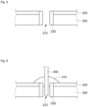
- the wire 400 may be inserted into the through-hole 310 and soldered, and then electrically connected. That is, as illustrated in FIG. 3 , since the wire 400 and the conductive pattern 320 on the board 300 do not contact each other in the process of inserting the wire 400 into the through-hole 310 as the conductive patterns 320 on the board 300 is spaced a predetermined distance from the through-hole 310 in another exemplary embodiment, the battery cells and the BMS 200 may not be electrically connected to each other before the soldering part 410 is formed.
- the exemplary embodiments allow the wire and the conductive pattern on the board not to be electrically connected with each other before the wire is inserted into the through-hole and soldered. That is, as the non-conductive layer is formed on the inside surface of the through-hole, the wire inserted to the through-hole may not be connected with the conductive pattern exposed to the inside of the through-hole or the conductive pattern on the board, and as the conductive pattern on the board is spaced a predetermined distance from the through-hole, the wire may not be connected with the conductive pattern on the board when inserted into the through-hole.
- the exemplary embodiment may prevent an electrical damage of the BMS when the wire extending from the battery cell is soldered on the board to connect the battery cell and the BMS. That is, even when the BMS is not connected sequentially from the battery cell of the low battery bank, an electrical damage may not be generated in the BMS.
- FIGS. 4 to 6 are views for explaining a method of manufacturing a battery apparatus in accordance with an exemplary embodiment.
- a through-hole 310 is formed in a predetermined area of the board 300.
- the board 300 may be a PCB on which a predetermined conductive pattern is formed. That is, the board 300 may be a PCB on which at least one insulation layer is formed and a predetermined conductive pattern is formed on the insulation layer. For example, the board 300 may be formed such that a plurality of insulation layers are laminated thereon, and a predetermined conductive pattern is formed between the insulation layers.
- a plurality of through-holes 310 may be formed in the predetermined area of the board 300.
- the through-holes 310 may be formed in various methods. For example, the through-holes 310 may be formed by using a pressing machine at a plurality of positions to which a plurality of wires extending from the battery cells are inserted.
- each of the through-holes 310 may be formed to have a diameter greater than that of the wire 400 extending from the battery cell, e.g., a diameter greater by two times to five times than that of the wire 400.
- the conductive pattern 320 may be formed on the board 300.
- the conductive pattern 320 may be formed as a predetermined pattern on an area except for the through-hole 310. That is, the conductive pattern 320 may be formed as a predetermined pattern from an extension line extending perpendicular to the inside surface of the through-hole 310.
- the conductive pattern 320 may be formed around the through-hole 310 from an area coinciding with the inside surface of the through-hole 310 in a vertical direction.
- a non-conductive layer 330 is formed on the inside surface of the through-hole 310.
- the non-conductive layer 330 may be formed by applying an insulating material on the inside surface of the through-hole 310, and thus the through-hole 310 may have a diameter less than an initially formed diameter thereof. That is, the through-hole 310 may be formed to have a first diameter, and as the non-conductive layer 330 is formed on the inside surface of the through-hole 310, the through-hole 310 may have a second diameter less than the first diameter after the non-conductive layer 330 is formed.
- the diameter of the through-hole 310 after the non-conductive layer 330 is formed may be also greater than that of the wire 400.
- the through-hole 310 may have a diameter greater by 1.5 times to 3 times than that of the wire 400.
- the insulation layer may be remained on the inside surface of the through-hole 310 by applying an insulating material to cover the through-hole 310 and then removing the insulation layer on the board and penetrating the through-hole 310 again.
- a soldering part 410 is formed by inserting the wire 400 inside the through-hole 310 and then soldering an upper side of the wire 400.
- the wire 400 and the conductive pattern 320 may be electrically connected to each other by the soldering part 410.
- the method of manufacturing the battery apparatus in accordance with an exemplary embodiment may include: a process of preparing at least one battery pack 100 including a plurality of battery cells 111 and 112; a process of forming a plurality of wires 400 connected with the plurality of battery cells 111 and 112; a process of providing the board 300 on which at least one insulation layer and a conductive layer are formed and forming the through-hole 310 therein; a process of forming the conductive pattern 320 around the through-hole 310 on the board 300; a process of forming the non-conductive layer 330 on the inside surface of the through-hole 310; a process of inserting the wire 400 inside the non-conductive layer 330 of the through-hole 310; and a process of forming the soldering part 410 connecting the wire 400 and the conductive pattern 320 by soldering the wire 400 above the board 300.
- the BMS 200 may be mounted onto the board 300 before the wire 400 is inserted after the non-conductive layer 330 is formed inside the through-
- the through-hole 310 may be formed before the conductive pattern 320 is formed, the non-conductive layer 330 may be formed on the inside surface of the through-hole 310, and then the conductive pattern 320 may be formed around the through-hole 310 on the board 300.
- a modified example of the method of manufacturing the battery apparatus in accordance with an exemplary embodiment may include: a process of forming the through-hole 310 in the board 300; a process of forming the non-conductive layer 330 on the inside surface of the through-hole 310; a process of forming the conductive pattern on the board 300 around the through-hole 310; a process of inserting the wire 400 inside the non-conductive layer 330 of the through-hole 310; and a process of forming the soldering part 410 connecting the wire 400 and the conductive pattern 320 by soldering the wire 400 above the board 300.
- the soldering part 410 may be formed by soldering the wire 400 above the board 300 after the non-conductive layer 330 is formed on the inside surface of the through-hole 310, and the wire 400 is inserted inside the non-conductive layer 330. Since the non-conductive layer 330 is formed on the inside surface of the through-hole 310, the wire 400 may not contact the conductive pattern 320 on the board 300 in a process of inserting the wire 400 into the through-hole 310, and the battery cells and the BMS 200 may not be electrically connected to each other before the soldering part 410 is formed. That is, as the inside of the through-hole 310 to which the wire 400 is inserted is not plated in an exemplary embodiment, the battery cells and the BMS 200 may not be electrically connected to each other before the soldering part 410 is formed.
- FIGS. 7 to 8 are views for explaining a method of manufacturing a battery apparatus in accordance with another exemplary embodiment.
- a description of another exemplary embodiment, which is overlapped with that of an exemplary embodiment, will be omitted, and a feature that is not mentioned in the description of another exemplary embodiment is as same as that of an exemplary embodiment.
- a through-hole 310 is formed in a predetermined area of a board 300.
- the board 300 may be a PCB on which a predetermined conductive pattern is formed.
- a plurality of through-holes 310 may be formed in the predetermined area of the board 300.
- the through-holes 310 may be formed in various methods.
- the through-holes 310 may be formed by using a pressing machine at a plurality of positions to which a plurality of wires extending from the battery cells are inserted.
- each of the through-holes 310 may be formed to have a diameter greater than that of the wire 400 extending from the battery cell.
- a conductive pattern 320 may be formed on the board 300.
- the conductive pattern 320 may be formed as a predetermined pattern on an area except for the through-hole 310.
- the conductive pattern 320 may be spaced a predetermined distance from the through-hole 310.
- the conductive pattern 320 may be spaced by about 0.3 mm from an outer circumference of the through-hole 310.
- the spaced distance between the conductive pattern 320 and the through-hole 310 requires maintaining a distance by which the wire 400 does not contact the conductive pattern 320 when inserted into the through-hole 310.
- the spaced distance between the conductive pattern 320 and the through-hole 310 requires maintaining a distance preventing a size of the soldering part 410 from increasing too much because the size of the soldering part 410 increases too much when the spaced distance therebetween is extremely large.
- the spaced distance between the conductive pattern 320 and the through-hole 310 may maintain a distance in a range from 0.3 mm to 1 mm in consideration of a size of the through-hole 310, a thickness of the wire 400, and a size of the soldering part 410.
- the soldering part 410 is formed by inserting the wire 400 inside the through-hole 310 and then soldering an upper side of the wire 400.
- the wire 400 and the conductive pattern 320 may be electrically connected to each other by the soldering part 410.
- the method of manufacturing the battery apparatus in accordance with another exemplary embodiment may include: a process of preparing at least one battery pack 100 including a plurality of battery cells 111 and 112; a process of forming a plurality of wires 400 connected with the plurality of battery cells 111 and 112; a process of preparing the board 300 on which at least one insulation layer and a conductive layer are laminated and a battery management system (BMS) is mounted; a process of forming the through-hole 310 in the board 300; a process of forming the conductive pattern 320 around the through-hole 310 on the board 300; a process of inserting the wire 400 inside the through-hole 310; and a process of forming the soldering part 410 connecting the wire 400 and the conductive pattern 320 by soldering the wire 400 above the board 300.
- BMS battery management system
- the conductive pattern 320 may be firstly formed in consideration of an area in which the through-hole 310 is to be formed, and then the through-hole 310 may be formed to be spaced apart from the conductive pattern 320.
- a modified example of the method of manufacturing the battery apparatus in accordance with another exemplary embodiment may include: a process of forming the conductive pattern 320 on the board 300; a process of forming the through-hole 310 inside the conductive pattern 320; a process of inserting the wire 400 inside the through-hole 310; and a process of forming the soldering part 410 connecting the wire 400 and the conductive pattern 320 by soldering the wire 400 above the board 300.
- the conductive pattern 320 may be formed on the board 300 so as to be spaced apart from the through-hole 310, and the soldering part 410 may be formed by soldering the wire 400 above the board 300 after the wire 400 is inserted into the through-hole 310. Since the conductive pattern 320 is formed on the board 300 while being spaced apart from the through-hole 310, the wire 400 may not contact the conductive pattern 320 on the board 300 in the process of inserting the wire 400 into the through-hole 310, and the battery cells and the BMS 200 may not be electrically connected to each other before the soldering part 410 is formed.
Landscapes
- Engineering & Computer Science (AREA)
- Chemical & Material Sciences (AREA)
- Chemical Kinetics & Catalysis (AREA)
- Electrochemistry (AREA)
- General Chemical & Material Sciences (AREA)
- Manufacturing & Machinery (AREA)
- Microelectronics & Electronic Packaging (AREA)
- Inorganic Chemistry (AREA)
- Connection Of Batteries Or Terminals (AREA)
- Battery Mounting, Suspending (AREA)
- Secondary Cells (AREA)
Abstract
Description
- The present invention relates to a battery apparatus and a method of manufacturing the same, and more particularly, to a battery apparatus capable of preventing an electrical damage of a battery management system (BMS) when a wire extending from a battery cell is soldered onto a board to connect the battery cell and the BMS and a method of manufacturing the same.
- A chargeable secondary battery, i.e., a battery, has been widely used as an energy source of a mobile device such as a smartphone. Furthermore, the battery has been used as an energy source of an electric vehicle and a hybrid electric vehicle, which are suggested as a measure for solving a limitation such as air pollution caused by a gasoline vehicle or a diesel vehicle, which uses a fossil fuel.
- The kind of applications using the battery is extremely diversified due to an advantageous aspect of the battery, and the battery is expected to be applied to more fields and products than now.
- The battery is classified into a lithium-ion battery, a lithium-ion-polymer battery, and a lithium-polymer battery according to a configuration of an electrode and an electrolyte, and the lithium-ion-polymer battery that has a low risk of leakage of the electrolyte and is easily manufactured has been increasingly used.
- As described above, the battery has been widely used as an energy source of various products. However, since the battery contains all sorts of combustible materials, the battery has a risk of heating and explosion caused by overcharge, overcurrent, and other physical impacts. In order to prevent the above-described limitation, the battery includes a safety system such as a protection circuit for blocking a current in case of overcharge, overdischarge, and overcurrent, a positive temperature coefficient (PTC) element having a resistance that extremely increases when a temperature increases to block a current, and a safety vent for exhausting a gas or blocking a current when a pressure increases due to gas generation. A medium and large sized battery pack having a structure in which a plurality of battery modules are combined includes a safety system such as a fuse, a bimetal, or a battery management system (BMS) for protecting a battery cell against overdischarge, overcharge, and overcurrent.
- Among the safety systems, the BMS is electrically connected with a plurality of battery cells configuring the battery pack. Here, one battery bank is configured as at least two battery cells are connected in parallel, and the battery pack includes at least two battery banks.
- A wire extending from the battery cell to connect the BMS with the battery cells extends onto a board to which the BMS is mounted and is soldered onto the board to connect the battery cell with the BMS. As a through-hole is formed in the board, the wire is inserted into the through-hole, and as the wire above the through-hole is soldered, the BMS mounted on the board and the battery cell are connected through the wire. Here, the battery cells are necessarily connected to the BMS sequentially from a low battery cell to a high battery cell of the battery bank to blocking an electrical damage to at least one integrated circuit (IC) among a plurality of ICs configuring the BMS. For example, when first to eighth battery banks are provided from the top to the bottom, and first to n-th battery cells are arranged in each battery bank, the battery cells are connected to the BMS from the n-th battery cell to the first battery cell of the eighth battery bank, and, in the same manner, the battery cells from the eighth battery bank to the first battery bank are sequentially connected to the BMS.
- However, when the battery banks are not sequentially soldered from the low battery bank, as a cell power is applied randomly to the BMS IC, an electrical damage may occur. That is, a power for operating the IC is received from the battery cell, and when a ground is not firstly connected, e.g., an intermediate battery cell among the first to n-th battery cells is firstly connected, a voltage of 4.2V or more is applied to an input pin of the IC, and two or more battery cells are connected although not allowed to cause an electrical damage as a voltage greater than an allowable voltage is applied to the IC. The electrical damage causes a malfunction of the IC as a current or a voltage greater than an allowable value is applied.
-
- (Patent document 1)
Korean Patent Registration No. 10-1572650 - (Patent document 2)
Korean Patent Publication No. 2018-0118920 - The present disclosure provides a battery apparatus capable of preventing an electrical damage of a battery management system (BMS) when a wire extending from a battery cell is soldered onto a board to connect the battery cell and the BMS and a method of manufacturing the same.
- The present disclosure also provides a battery apparatus preventing an electrical damage of a BMS even when the BMS is not connected sequentially from a battery cell of a low battery bank and a method of manufacturing the same.
- In accordance with an exemplary embodiment, a battery apparatus includes: at least one battery pack including a plurality of battery cells; a battery management system (BMS) configured to manage the plurality of battery cells; a board to which the BMS is mounted and on which at least one insulation layer and a conductive layer are laminated; a plurality of wires extending from the battery cells onto the board; a plurality of through-holes which are formed in the board and to which the plurality of wires are respectively inserted; a non-conductive area formed on at least one area around the through-hole; and a soldering part formed on the through-hole to which the wire is inserted.
- The battery apparatus may further include a conductive pattern formed on the board, connected with the BMS, and connected with the wire by the soldering part.
- The non-conductive area may include a non-conductive layer formed on an inside surface of the through-hole.
- The non-conductive layer may be made of a material different from that of the insulation layer of the board.
- The non-conductive area may include a conductive pattern spaced by a predetermined distance from an outer circumference of the through-hole.
- The conductive pattern may be spaced by 0.3 mm to 1 mm from the outer circumference of the through-hole.
- In accordance with another exemplary embodiment, a method of manufacturing a battery apparatus includes processes of: forming a through-hole in a board on which at least one insulation layer and a conductive layer are laminated; forming a conductive pattern on the board around the through-hole; forming a non-conductive layer on an inside surface of the through-hole; inserting a wire extending from a plurality of battery cells to the inside of the non-conductive layer of the through-hole; and forming a soldering part configured to connect the wire above the through-hole with the conductive pattern.
- The method may further include a process of mounting a BMS on the board before inserting the wire after the non-conductive layer is formed.
- The conductive pattern may be formed on the board from an outer circumference of the through-hole.
- The non-conductive layer may be made of a material different from that of the insulation layer of the board.
- In accordance with still another exemplary embodiment, a method of manufacturing a battery apparatus includes processes of: forming a plurality of through-holes in a board; forming a conductive pattern on a board around the through-hole; inserting a wire extending from a plurality of battery cells to the inside of the through-hole; and forming a soldering part configured to connect the wire above the through-hole with the conductive pattern, and the conductive pattern is spaced by a predetermined distance from an outer circumference of the through-hole.
- The conductive pattern may be formed on an area spaced by 0.3 mm to 1 mm from the outer circumference of the through-hole.
- In the present invention, the wire may not be electrically connected with the conductive pattern on the board before the wire is inserted into the through-hole and soldered. That is, as the insulation layer is formed on the inside surface of the through-hole, the wire inserted to the through-hole may not be connected with the conductive pattern exposed to the inside of the through-hole or the conductive pattern on the board, and as the conductive pattern on the board is spaced a predetermined distance from the through-hole, the wire may not be connected with the conductive pattern on the board when inserted into the through-hole.
- Thus, the present invention may prevent the electrical damage of the BMS when the wire extending from the battery cell is soldered onto the board to connect the battery cell and the BMS. That is, even when the BMS is not connected sequentially from the battery cell of the low battery bank, the electrical damage may not be generated in the BMS.
- Exemplary embodiments can be understood in more detail from the following description taken in conjunction with the accompanying drawings, in which:
-
FIG. 1 is a block diagram for explaining a configuration of a battery apparatus in accordance with exemplary embodiments; -
FIGS. 2 and3 are partial cross-sectional views respectively illustrating battery apparatuses in accordance with an exemplary embodiment and another exemplary embodiment; -
FIGS. 4 to 6 are views for explaining a method of manufacturing a battery apparatus in accordance with an exemplary embodiment; and -
FIGS. 7 to 8 are views for explaining a method of manufacturing a battery apparatus in accordance with another exemplary embodiment. - Hereinafter, specific embodiments will be described in detail with reference to the accompanying drawings. The present disclosure may, however, be embodied in different forms and should not be construed as limited to the embodiments set forth herein. Rather, these embodiments are provided so that this disclosure will be thorough and complete, and will fully convey the scope of the present disclosure to those skilled in the art. In the figures, the dimensions of layers and regions are exaggerated for clarity of illustration. Like reference numerals refer to like elements throughout.
-
FIG. 1 is a block diagram for explaining a configuration of a battery apparatus in accordance with an exemplary embodiment. Also,FIGS. 2 and3 are partial cross-sectional views respectively illustrating battery apparatuses in accordance with an exemplary embodiment and another exemplary embodiment. That is,FIGS. 2 and3 are partial cross-sectional views respectively illustrating the battery apparatuses in which a wire inserted to a through-hole defined in a board is soldered in accordance with the exemplary embodiments. - Referring to
FIG. 1 , the battery apparatus in accordance with the exemplary embodiments may include: abattery pack 100 including a plurality ofbattery banks 110 to 150, a battery management system (BMS) 200 for managing thebattery pack 100; aboard 300 on which the BMS is mounted; awire 400 extending from thebattery pack 100 to connect a battery cell and theBMS 200 on theboard 300; and a soldering part for fixing thewire 400 on theboard 300 for electrically connection therebeteween. The configuration of the battery apparatus in accordance with an exemplary embodiment will be described in detail below. - The battery pack 100 supplies electric energy to applications such as a smartphone or an electric vehicle. The
battery pack 100 may be managed by the BMS 200 and charged by an external power. Here, thebattery pack 100 may include a plurality ofbattery banks 110 to 150. Also, each of thebattery banks 110 to 150 may include a plurality ofchargeable battery cells battery banks 110 to 150 includes twobattery cells battery banks 110 to 150 may include two ormore battery cells battery cells first battery bank 110 inFIG. 1 , since each of therest battery banks 120 to 150 also includes the same number of battery cells having the same connection relationship, reference numerals are not applied to the battery cells of thebattery banks 120 to 150. Hereinafter, thebattery cells battery banks 120 to 150. Also, thebattery cells battery banks 110 to 150 may be connected in parallel. For example, thebattery cells first battery bank 110 may be connected in parallel, and thebattery cells fifth battery banks 120 to 150 may be also connected in parallel. However, thebattery cells battery cells battery cells battery cells battery cells - The
BMS 200 estimates a state of thebattery pack 100 and manages thebattery pack 100 by using estimated state information. For example, the state information of thebattery pack 100 such as SOC, a state of health (SOH), a maximum input-output power allowance, and an output voltage is estimated and managed. Also, charge or discharge of thebattery pack 100 is controlled by using the state information. The BMS in accordance with an exemplary embodiment includes a SOC estimation device for estimating a SOC of thebattery pack 100. Also, theBMS 200 controls cell balancing for balancing a charge state of each battery cell. That is, thebattery cell battery cell battery pack 100 to manage thebattery pack 100 by using theBMS 200 may be further provided. The sensing part may include a current sensor for sensing a current of thebattery pack 100, a voltage sensor for sensing a voltage of thebattery pack 100, and a temperature sensor for sensing a temperature of thebattery pack 100. Here, at least one current sensor, at least one voltage sensor, and at least one temperature sensor may be provided. The BMS performing the above-described various functions may include various components and be mounted on theboard 300. That is, a plurality of components for estimating the SOC, a plurality of components for cell balancing, a plurality of components for configuring the sensing part, and other passive elements may be mounted on theboard 300. Although not shown, a charge-discharge protection circuit for protecting thebattery pack 100 by controlling the charge-discharge of thebattery pack 100 may be further provided. That is, the charge-discharge protection circuit may be mounted on theboard 300 as a component separated from theBMS 200. - The
board 300 may include a printed circuit board (PCB) in which a circuit pattern is formed on an insulation layer. The necessary circuit pattern of the PCB is formed by attaching a copper thin plate to a surface of a phenol-resin insulation layer or an epoxy-resin insulation layer and then etching the copper thin plate according to a predetermined pattern, and the above-described PCB may be used as theboard 300. Here, a single sided board, a double sided board, and a multilayer board may be used as the PCB according to the circuit layer and the number of the insulation layers, and since the board having a large number of layers exhibits an excellent mounting capacity of electronic components and is used for a high-precision product, the number of layers may be selected according to the number and the degree of integration of components mounted to the PCB. In addition to a plurality of components configuring theBMS 200, a passive element such as a capacitor, an inductor, and a resistor may be mounted on theboard 300. Also, a plurality of through-holes 310 may be defined in theboard 300. Also, a predeterminedconductive pattern 320 may be formed on a top surface of theboard 300. Here, theconductive pattern 320 may be formed around the through-hole 310 on theboard 300. Theconductive pattern 320 may be connected to at least one component mounted on theboard 300. That is, theconductive pattern 320 may be connected to at least a portion of theBMS 200. - The
wire 400 may connect thebattery cells battery banks 110 to 150 with theBMS 200. That is, thewire 400 may extend from thebattery cells board 300 and be connected with theBMS 200. Here, thewire 400 may be made of, e.g., copper, aluminum, or an alloy thereof. Thewire 400 may extend from thebattery cells board 300 and be inserted to the through-hole 310 of theboard 300. Also, as asoldering part 410 is formed at an upper side of the through-hole 310 by soldering after thewire 400 is inserted to the through-hole 310, thewire 400 may be connected to theconductive pattern 320 on theboard 300, and thus thebattery pack 100 and theBMS 200 may be electrically connected to each other. - Here, as the inside of the through-
hole 310 to which thewire 400 is inserted is not plated in an exemplary embodiment, thebattery cells BMS 200 may not be electrically connected to each other before thesoldering part 410 is formed. That is, as illustrated inFIG. 2 , in accordance with an exemplary embodiment, thesoldering part 410 may be formed by soldering thewire 400 above theboard 300 after anon-conductive layer 330 is formed on an inside surface of the through-hole 310, and thewire 400 is inserted inside thenon-conductive layer 330. Since thenon-conductive layer 330 is formed on the inside surface of the through-hole 310, thewire 400 may not contact a conductive material, e.g., theconductive pattern 320 on theboard 300 in a process of inserting thewire 400 into the through-hole 310, and the battery cells and theBMS 200 may not be electrically connected to each other before thesoldering part 410 is formed. Here, thenon-conductive layer 330 may be made of a different kind of material from theboard 300. That is, thenon-conductive layer 330 may be made of a material different from the insulation layer of theboard 300. Alternatively, thenon-conductive layer 330 may be made of the same material as the insulation layer of theboard 300. Here, thenon-conductive layer 330 may be formed in a following process after the insulation layer and the conductive layer of theboard 300 are formed. That is, theboard 300 may be manufactured into the PCB on which the plurality of insulation layers and the conductive pattern are laminated and in which the through-hole 310 is formed, and then thenon-conducive layer 330 in the through-hole 310 may be formed on the inside surface of the through-hole 310 in a following process. - Also, in another exemplary embodiment, as the
conductive pattern 320 is not formed around at the upper side of the through-hole 310, thewire 400 may be inserted into the through-hole 310 and soldered, and then electrically connected. That is, as illustrated inFIG. 3 , since thewire 400 and theconductive pattern 320 on theboard 300 do not contact each other in the process of inserting thewire 400 into the through-hole 310 as theconductive patterns 320 on theboard 300 is spaced a predetermined distance from the through-hole 310 in another exemplary embodiment, the battery cells and theBMS 200 may not be electrically connected to each other before thesoldering part 410 is formed. - As described above, the exemplary embodiments allow the wire and the conductive pattern on the board not to be electrically connected with each other before the wire is inserted into the through-hole and soldered. That is, as the non-conductive layer is formed on the inside surface of the through-hole, the wire inserted to the through-hole may not be connected with the conductive pattern exposed to the inside of the through-hole or the conductive pattern on the board, and as the conductive pattern on the board is spaced a predetermined distance from the through-hole, the wire may not be connected with the conductive pattern on the board when inserted into the through-hole. Thus, the exemplary embodiment may prevent an electrical damage of the BMS when the wire extending from the battery cell is soldered on the board to connect the battery cell and the BMS. That is, even when the BMS is not connected sequentially from the battery cell of the low battery bank, an electrical damage may not be generated in the BMS.
- A method of manufacturing the battery apparatus in accordance with exemplary embodiments will be described with reference to the drawings. Here, the exemplary embodiments describe the manufacturing method focused on the through-hole defined in the board.
-
FIGS. 4 to 6 are views for explaining a method of manufacturing a battery apparatus in accordance with an exemplary embodiment. - Referring to
FIG. 4 , a through-hole 310 is formed in a predetermined area of theboard 300. - The
board 300 may be a PCB on which a predetermined conductive pattern is formed. That is, theboard 300 may be a PCB on which at least one insulation layer is formed and a predetermined conductive pattern is formed on the insulation layer. For example, theboard 300 may be formed such that a plurality of insulation layers are laminated thereon, and a predetermined conductive pattern is formed between the insulation layers. A plurality of through-holes 310 may be formed in the predetermined area of theboard 300. The through-holes 310 may be formed in various methods. For example, the through-holes 310 may be formed by using a pressing machine at a plurality of positions to which a plurality of wires extending from the battery cells are inserted. Here, each of the through-holes 310 may be formed to have a diameter greater than that of thewire 400 extending from the battery cell, e.g., a diameter greater by two times to five times than that of thewire 400. Also, theconductive pattern 320 may be formed on theboard 300. Here, theconductive pattern 320 may be formed as a predetermined pattern on an area except for the through-hole 310. That is, theconductive pattern 320 may be formed as a predetermined pattern from an extension line extending perpendicular to the inside surface of the through-hole 310. In other words, theconductive pattern 320 may be formed around the through-hole 310 from an area coinciding with the inside surface of the through-hole 310 in a vertical direction. - Referring to
FIG. 5 , anon-conductive layer 330 is formed on the inside surface of the through-hole 310. - The
non-conductive layer 330 may be formed by applying an insulating material on the inside surface of the through-hole 310, and thus the through-hole 310 may have a diameter less than an initially formed diameter thereof. That is, the through-hole 310 may be formed to have a first diameter, and as thenon-conductive layer 330 is formed on the inside surface of the through-hole 310, the through-hole 310 may have a second diameter less than the first diameter after thenon-conductive layer 330 is formed. Here, the diameter of the through-hole 310 after thenon-conductive layer 330 is formed may be also greater than that of thewire 400. For example, the through-hole 310 may have a diameter greater by 1.5 times to 3 times than that of thewire 400. Various processes may be used to form thenon-conductive layer 330 on the inside surface of the through-hole 310. For example, the insulation layer may be remained on the inside surface of the through-hole 310 by applying an insulating material to cover the through-hole 310 and then removing the insulation layer on the board and penetrating the through-hole 310 again. - Referring to
FIG. 6 , asoldering part 410 is formed by inserting thewire 400 inside the through-hole 310 and then soldering an upper side of thewire 400. Thus, thewire 400 and theconductive pattern 320 may be electrically connected to each other by thesoldering part 410. - That is, the method of manufacturing the battery apparatus in accordance with an exemplary embodiment may include: a process of preparing at least one
battery pack 100 including a plurality ofbattery cells wires 400 connected with the plurality ofbattery cells board 300 on which at least one insulation layer and a conductive layer are formed and forming the through-hole 310 therein; a process of forming theconductive pattern 320 around the through-hole 310 on theboard 300; a process of forming thenon-conductive layer 330 on the inside surface of the through-hole 310; a process of inserting thewire 400 inside thenon-conductive layer 330 of the through-hole 310; and a process of forming thesoldering part 410 connecting thewire 400 and theconductive pattern 320 by soldering thewire 400 above theboard 300. Here, theBMS 200 may be mounted onto theboard 300 before thewire 400 is inserted after thenon-conductive layer 330 is formed inside the through-hole 310. - Also, an exemplary embodiment described with reference to
FIGS. 4 to 6 may be modified in various methods. For example, the through-hole 310 may be formed before theconductive pattern 320 is formed, thenon-conductive layer 330 may be formed on the inside surface of the through-hole 310, and then theconductive pattern 320 may be formed around the through-hole 310 on theboard 300. That is, a modified example of the method of manufacturing the battery apparatus in accordance with an exemplary embodiment may include: a process of forming the through-hole 310 in theboard 300; a process of forming thenon-conductive layer 330 on the inside surface of the through-hole 310; a process of forming the conductive pattern on theboard 300 around the through-hole 310; a process of inserting thewire 400 inside thenon-conductive layer 330 of the through-hole 310; and a process of forming thesoldering part 410 connecting thewire 400 and theconductive pattern 320 by soldering thewire 400 above theboard 300. - As described above, in accordance with an exemplary embodiment, the
soldering part 410 may be formed by soldering thewire 400 above theboard 300 after thenon-conductive layer 330 is formed on the inside surface of the through-hole 310, and thewire 400 is inserted inside thenon-conductive layer 330. Since thenon-conductive layer 330 is formed on the inside surface of the through-hole 310, thewire 400 may not contact theconductive pattern 320 on theboard 300 in a process of inserting thewire 400 into the through-hole 310, and the battery cells and theBMS 200 may not be electrically connected to each other before thesoldering part 410 is formed. That is, as the inside of the through-hole 310 to which thewire 400 is inserted is not plated in an exemplary embodiment, the battery cells and theBMS 200 may not be electrically connected to each other before thesoldering part 410 is formed. -
FIGS. 7 to 8 are views for explaining a method of manufacturing a battery apparatus in accordance with another exemplary embodiment. Here, a description of another exemplary embodiment, which is overlapped with that of an exemplary embodiment, will be omitted, and a feature that is not mentioned in the description of another exemplary embodiment is as same as that of an exemplary embodiment. - Referring to
FIG. 7 , a through-hole 310 is formed in a predetermined area of aboard 300. - The
board 300 may be a PCB on which a predetermined conductive pattern is formed. A plurality of through-holes 310 may be formed in the predetermined area of theboard 300. The through-holes 310 may be formed in various methods. For example, the through-holes 310 may be formed by using a pressing machine at a plurality of positions to which a plurality of wires extending from the battery cells are inserted. Here, each of the through-holes 310 may be formed to have a diameter greater than that of thewire 400 extending from the battery cell. Also, aconductive pattern 320 may be formed on theboard 300. Here, theconductive pattern 320 may be formed as a predetermined pattern on an area except for the through-hole 310. Also, theconductive pattern 320 may be spaced a predetermined distance from the through-hole 310. For example, theconductive pattern 320 may be spaced by about 0.3 mm from an outer circumference of the through-hole 310. Here, the spaced distance between theconductive pattern 320 and the through-hole 310 requires maintaining a distance by which thewire 400 does not contact theconductive pattern 320 when inserted into the through-hole 310. Also, the spaced distance between theconductive pattern 320 and the through-hole 310 requires maintaining a distance preventing a size of thesoldering part 410 from increasing too much because the size of thesoldering part 410 increases too much when the spaced distance therebetween is extremely large. Thus, the spaced distance between theconductive pattern 320 and the through-hole 310 may maintain a distance in a range from 0.3 mm to 1 mm in consideration of a size of the through-hole 310, a thickness of thewire 400, and a size of thesoldering part 410. - Referring to
FIG. 8 , thesoldering part 410 is formed by inserting thewire 400 inside the through-hole 310 and then soldering an upper side of thewire 400. Thus, thewire 400 and theconductive pattern 320 may be electrically connected to each other by thesoldering part 410. - That is, the method of manufacturing the battery apparatus in accordance with another exemplary embodiment may include: a process of preparing at least one
battery pack 100 including a plurality ofbattery cells wires 400 connected with the plurality ofbattery cells board 300 on which at least one insulation layer and a conductive layer are laminated and a battery management system (BMS) is mounted; a process of forming the through-hole 310 in theboard 300; a process of forming theconductive pattern 320 around the through-hole 310 on theboard 300; a process of inserting thewire 400 inside the through-hole 310; and a process of forming thesoldering part 410 connecting thewire 400 and theconductive pattern 320 by soldering thewire 400 above theboard 300. - Here, another exemplary embodiment may be modified in various methods. For example, the
conductive pattern 320 may be firstly formed in consideration of an area in which the through-hole 310 is to be formed, and then the through-hole 310 may be formed to be spaced apart from theconductive pattern 320. That is, a modified example of the method of manufacturing the battery apparatus in accordance with another exemplary embodiment may include: a process of forming theconductive pattern 320 on theboard 300; a process of forming the through-hole 310 inside theconductive pattern 320; a process of inserting thewire 400 inside the through-hole 310; and a process of forming thesoldering part 410 connecting thewire 400 and theconductive pattern 320 by soldering thewire 400 above theboard 300. - As described above, in accordance with another exemplary embodiment, the
conductive pattern 320 may be formed on theboard 300 so as to be spaced apart from the through-hole 310, and thesoldering part 410 may be formed by soldering thewire 400 above theboard 300 after thewire 400 is inserted into the through-hole 310. Since theconductive pattern 320 is formed on theboard 300 while being spaced apart from the through-hole 310, thewire 400 may not contact theconductive pattern 320 on theboard 300 in the process of inserting thewire 400 into the through-hole 310, and the battery cells and theBMS 200 may not be electrically connected to each other before thesoldering part 410 is formed. - As described above, the technical idea of the present invention has been specifically described with respect to the above embodiments, but it should be noted that the foregoing embodiments are provided only for illustration while not limiting the present invention. Various embodiments may be provided to allow those skilled in the art to understand the scope of the preset invention, but the present invention is not limited thereto.
- Description of Reference Numerals in the drawings of the present invention is given below.
100 battery pack 200 BMS 300 board 400 wire
Claims (12)
- A battery apparatus comprising:at least one battery pack comprising a plurality of battery cells;a battery management system BMS configured to manage the plurality of battery cells;a board to which the BMS is mounted and on which at least one insulation layer and a conductive layer are laminated;a plurality of wires extending from the plurality of battery cells onto the board;a plurality of through-holes which are formed in the board and to which the plurality of wires are respectively inserted;a non-conductive area formed on at least one area around the through-hole; anda soldering part formed on the through-hole to which the wire is inserted.
- The battery apparatus of claim 1, further comprising a conductive pattern formed on the board, connected with the BMS, and connected with the wire by the soldering part.
- The battery apparatus of claim 1 or 2, wherein the non-conductive area comprises a non-conductive layer formed on an inside surface of the through-hole.
- The battery apparatus of claim 3, wherein the non-conductive layer is made of a material different from that of the insulation layer of the board.
- The battery apparatus of claim 1, wherein the non-conductive area comprises a conductive pattern spaced by a predetermined distance from an outer circumference of the through-hole.
- The battery apparatus of claim 5, wherein the conductive pattern is spaced by 0.3 mm to 1 mm from the outer circumference of the through-hole.
- A method of manufacturing a battery apparatus, comprising processes of:forming a through-hole in a board on which at least one insulation layer and a conductive layer are laminated;forming a conductive pattern on the board around the through-hole;forming a non-conductive layer on an inside surface of the through-hole;inserting a wire extending from a plurality of battery cells to the inside of the non-conductive layer of the through-hole; andforming a soldering part configured to connect the wire above the through-hole with the conductive pattern.
- The method of claim 7, further comprising a process of mounting a BMS on the board before inserting the wire after the non-conductive layer is formed.
- The method of claim 7 or 8, wherein the conductive pattern is formed on the board from an outer circumference of the through-hole.
- The method of claim 7 or 8, wherein the non-conductive layer is made of a material different from that of the insulation layer of the board.
- A method of manufacturing a battery apparatus, comprising processes of:forming a plurality of through-holes in a board;forming a conductive pattern on a board around the through-hole;inserting a wire extending from a plurality of battery cells to the inside of the through-hole; andforming a soldering part configured to connect the wire above the through-hole with the conductive pattern,wherein the conductive pattern is spaced by a predetermined distance from an outer circumference of the through-hole.
- The method of claim 11, wherein the conductive pattern is formed on an area spaced by 0.3 mm to 1 mm from the outer circumference of the through-hole.
Applications Claiming Priority (2)
| Application Number | Priority Date | Filing Date | Title |
|---|---|---|---|
| KR1020200100658A KR102847231B1 (en) | 2020-08-11 | 2020-08-11 | Battery apparatus and method of manufacturing the same |
| PCT/KR2021/010081 WO2022035108A1 (en) | 2020-08-11 | 2021-08-02 | Battery apparatus and manufacturing method therefor |
Publications (3)
| Publication Number | Publication Date |
|---|---|
| EP4135096A1 true EP4135096A1 (en) | 2023-02-15 |
| EP4135096A4 EP4135096A4 (en) | 2024-07-31 |
| EP4135096B1 EP4135096B1 (en) | 2025-04-09 |
Family
ID=80247138
Family Applications (1)
| Application Number | Title | Priority Date | Filing Date |
|---|---|---|---|
| EP21856114.0A Active EP4135096B1 (en) | 2020-08-11 | 2021-08-02 | Battery apparatus and manufacturing method therefor |
Country Status (9)
| Country | Link |
|---|---|
| US (1) | US12580234B2 (en) |
| EP (1) | EP4135096B1 (en) |
| JP (1) | JP7531611B2 (en) |
| KR (1) | KR102847231B1 (en) |
| CN (1) | CN115516692B (en) |
| ES (1) | ES3022907T3 (en) |
| HU (1) | HUE070870T2 (en) |
| TW (1) | TW202213851A (en) |
| WO (1) | WO2022035108A1 (en) |
Cited By (1)
| Publication number | Priority date | Publication date | Assignee | Title |
|---|---|---|---|---|
| WO2024145633A1 (en) * | 2022-12-29 | 2024-07-04 | Cps Technology Holdings Llc | Lead assembly pin guide |
Families Citing this family (1)
| Publication number | Priority date | Publication date | Assignee | Title |
|---|---|---|---|---|
| KR102930126B1 (en) * | 2020-10-14 | 2026-02-25 | 주식회사 엘지에너지솔루션 | Battery apparatus |
Family Cites Families (23)
| Publication number | Priority date | Publication date | Assignee | Title |
|---|---|---|---|---|
| JPH08288647A (en) | 1995-04-12 | 1996-11-01 | Fujitsu Ltd | Method for manufacturing printed wiring board and printed wiring board |
| JP4514243B2 (en) | 1997-12-05 | 2010-07-28 | パナソニック株式会社 | Terminal connection device for power circuit |
| US6541712B1 (en) | 2001-12-04 | 2003-04-01 | Teradyhe, Inc. | High speed multi-layer printed circuit board via |
| JP2004273988A (en) | 2003-03-12 | 2004-09-30 | Denso Corp | Circuit board and method of manufacturing the same |
| JP4564342B2 (en) | 2004-11-24 | 2010-10-20 | 大日本印刷株式会社 | Multilayer wiring board and manufacturing method thereof |
| KR100749655B1 (en) | 2005-12-20 | 2007-08-14 | 삼성에스디아이 주식회사 | Battery pack |
| KR100778987B1 (en) * | 2005-12-27 | 2007-11-22 | 삼성에스디아이 주식회사 | Battery pack |
| JP4946742B2 (en) * | 2007-09-05 | 2012-06-06 | ソニー株式会社 | Board, circuit board and battery pack |
| JP5111099B2 (en) | 2007-12-28 | 2012-12-26 | シャープ株式会社 | Battery pack |
| KR100965683B1 (en) | 2008-03-31 | 2010-06-24 | 삼성에스디아이 주식회사 | Battery pack |
| KR20110096245A (en) | 2010-02-22 | 2011-08-30 | 제이앤디써키트주식회사 | Manufacturing method of printed circuit board |
| BR112012021678B1 (en) | 2010-04-19 | 2021-04-06 | Nippon Steel Corporation | PUSH IN SCREW DEVICE AND ROLL MOLDING MACHINE |
| US9451710B2 (en) | 2010-08-26 | 2016-09-20 | Samsung Sdi Co., Ltd. | Battery pack |
| KR101245286B1 (en) * | 2011-06-10 | 2013-03-19 | 주식회사 엘지화학 | Connecting structure for secondary battery and Battery pack including the same |
| KR101853397B1 (en) | 2011-09-01 | 2018-04-30 | 엘지전자 주식회사 | Battery Module |
| KR20130085571A (en) | 2011-12-22 | 2013-07-30 | 삼성전기주식회사 | Fpc and coil connection module for spindle motor and spindle motor having the same |
| US8586217B2 (en) | 2011-12-22 | 2013-11-19 | Samsung Sdi Co., Ltd. | Protective circuit module |
| JP6022348B2 (en) * | 2012-12-27 | 2016-11-09 | 三洋電機株式会社 | Battery pack |
| KR101572650B1 (en) | 2013-02-19 | 2015-12-04 | 주식회사 엘지화학 | Apparatus and method for diagnosis of battery bank's imbalancing |
| US9966584B2 (en) | 2013-03-11 | 2018-05-08 | Atieva, Inc. | Bus bar for battery packs |
| KR101684358B1 (en) | 2013-09-30 | 2016-12-20 | 주식회사 엘지화학 | Battery Pack Having Electric Insulating Pack Case |
| KR101944007B1 (en) | 2015-12-16 | 2019-01-31 | 주식회사 네패스 | Semiconductor package and method of manufacturing the same |
| KR102269112B1 (en) | 2017-04-24 | 2021-06-24 | 주식회사 엘지화학 | Damping Member for Preventing Shake of BMS and Battery Module Having the Same |
-
2020
- 2020-08-11 KR KR1020200100658A patent/KR102847231B1/en active Active
-
2021
- 2021-08-02 JP JP2022567852A patent/JP7531611B2/en active Active
- 2021-08-02 HU HUE21856114A patent/HUE070870T2/en unknown
- 2021-08-02 CN CN202180033630.7A patent/CN115516692B/en active Active
- 2021-08-02 WO PCT/KR2021/010081 patent/WO2022035108A1/en not_active Ceased
- 2021-08-02 ES ES21856114T patent/ES3022907T3/en active Active
- 2021-08-02 US US17/925,796 patent/US12580234B2/en active Active
- 2021-08-02 EP EP21856114.0A patent/EP4135096B1/en active Active
- 2021-08-06 TW TW110129015A patent/TW202213851A/en unknown
Cited By (1)
| Publication number | Priority date | Publication date | Assignee | Title |
|---|---|---|---|---|
| WO2024145633A1 (en) * | 2022-12-29 | 2024-07-04 | Cps Technology Holdings Llc | Lead assembly pin guide |
Also Published As
| Publication number | Publication date |
|---|---|
| CN115516692B (en) | 2025-11-18 |
| JP2023525302A (en) | 2023-06-15 |
| EP4135096A4 (en) | 2024-07-31 |
| KR102847231B1 (en) | 2025-08-18 |
| WO2022035108A1 (en) | 2022-02-17 |
| CN115516692A (en) | 2022-12-23 |
| US20230207895A1 (en) | 2023-06-29 |
| KR20220020106A (en) | 2022-02-18 |
| HUE070870T2 (en) | 2025-07-28 |
| US12580234B2 (en) | 2026-03-17 |
| TW202213851A (en) | 2022-04-01 |
| JP7531611B2 (en) | 2024-08-09 |
| ES3022907T3 (en) | 2025-05-29 |
| EP4135096B1 (en) | 2025-04-09 |
Similar Documents
| Publication | Publication Date | Title |
|---|---|---|
| EP2378594B1 (en) | Secondary battery | |
| US6797018B2 (en) | Solid-state energy storage module employing integrated interconnect board | |
| US8057931B2 (en) | Battery busing scheme | |
| US10601018B2 (en) | Electrode lead for a secondary battery, a pouch type secondary battery and a battery module comprising the same | |
| KR102882949B1 (en) | Printed circuit board and battery apparatus having the same | |
| JPH11345604A (en) | Lithium secondary battery and battery module | |
| US9345146B2 (en) | Circuit board for secondary battery and secondary battery with the circuit board | |
| EP4135096B1 (en) | Battery apparatus and manufacturing method therefor | |
| KR102331064B1 (en) | Battery pack | |
| US20140292284A1 (en) | Electrical capacitor, electrical capacitor module, fabrication method of the electrical capacitor, and fabrication method of the electrical capacitor module | |
| KR102379765B1 (en) | The Secondary Battery And The Battery Module | |
| US8043735B2 (en) | Rechargeable battery, printed circuit board therefor, and method of fabricating the same | |
| KR20210158656A (en) | Method of manufacturing a circuit board, the circuit board manufactured thereby, electric vehicle having the circuit board | |
| US20210074986A1 (en) | Battery Cell and Method for Producing a Battery Cell | |
| CN223583141U (en) | Battery Module | |
| KR20210117044A (en) | The Secondary Battery And The Battery Module | |
| EP3385997A1 (en) | Secondary cell for a traction battery and method for manufacturing a secondary cell | |
| CN110352509A (en) | The method of the secondary battery cell and manufacture secondary battery cell of traction battery | |
| EP3944454A1 (en) | Pre-charge unit for charging a dc link capacitor and battery system comprising the same | |
| EP3454404B1 (en) | Method for joining an electrode stack | |
| US20110123840A1 (en) | Secondary battery | |
| KR20080048851A (en) | Battery pack | |
| KR20200052701A (en) | Protection circuit module |
Legal Events
| Date | Code | Title | Description |
|---|---|---|---|
| STAA | Information on the status of an ep patent application or granted ep patent |
Free format text: STATUS: THE INTERNATIONAL PUBLICATION HAS BEEN MADE |
|
| PUAI | Public reference made under article 153(3) epc to a published international application that has entered the european phase |
Free format text: ORIGINAL CODE: 0009012 |
|
| STAA | Information on the status of an ep patent application or granted ep patent |
Free format text: STATUS: REQUEST FOR EXAMINATION WAS MADE |
|
| 17P | Request for examination filed |
Effective date: 20221109 |
|
| AK | Designated contracting states |
Kind code of ref document: A1 Designated state(s): AL AT BE BG CH CY CZ DE DK EE ES FI FR GB GR HR HU IE IS IT LI LT LU LV MC MK MT NL NO PL PT RO RS SE SI SK SM TR |
|
| DAV | Request for validation of the european patent (deleted) | ||
| DAX | Request for extension of the european patent (deleted) | ||
| A4 | Supplementary search report drawn up and despatched |
Effective date: 20240703 |
|
| RIC1 | Information provided on ipc code assigned before grant |
Ipc: H05K 1/11 20060101ALI20240627BHEP Ipc: H01M 50/522 20210101ALI20240627BHEP Ipc: H01M 50/519 20210101ALI20240627BHEP Ipc: H01M 50/284 20210101ALI20240627BHEP Ipc: H01M 50/209 20210101ALI20240627BHEP Ipc: H01M 10/48 20060101ALI20240627BHEP Ipc: H05K 3/44 20060101ALI20240627BHEP Ipc: H01M 50/516 20210101ALI20240627BHEP Ipc: H01M 50/503 20210101ALI20240627BHEP Ipc: H01M 50/298 20210101ALI20240627BHEP Ipc: H05K 3/34 20060101ALI20240627BHEP Ipc: H05K 3/40 20060101ALI20240627BHEP Ipc: H01M 10/42 20060101AFI20240627BHEP |
|
| GRAP | Despatch of communication of intention to grant a patent |
Free format text: ORIGINAL CODE: EPIDOSNIGR1 |
|
| STAA | Information on the status of an ep patent application or granted ep patent |
Free format text: STATUS: GRANT OF PATENT IS INTENDED |
|
| INTG | Intention to grant announced |
Effective date: 20250114 |
|
| GRAS | Grant fee paid |
Free format text: ORIGINAL CODE: EPIDOSNIGR3 |
|
| GRAA | (expected) grant |
Free format text: ORIGINAL CODE: 0009210 |
|
| STAA | Information on the status of an ep patent application or granted ep patent |
Free format text: STATUS: THE PATENT HAS BEEN GRANTED |
|
| P01 | Opt-out of the competence of the unified patent court (upc) registered |
Free format text: CASE NUMBER: APP_6062/2025 Effective date: 20250205 |
|
| AK | Designated contracting states |
Kind code of ref document: B1 Designated state(s): AL AT BE BG CH CY CZ DE DK EE ES FI FR GB GR HR HU IE IS IT LI LT LU LV MC MK MT NL NO PL PT RO RS SE SI SK SM TR |
|
| REG | Reference to a national code |
Ref country code: GB Ref legal event code: FG4D |
|
| REG | Reference to a national code |
Ref country code: CH Ref legal event code: EP |
|
| REG | Reference to a national code |
Ref country code: DE Ref legal event code: R096 Ref document number: 602021029048 Country of ref document: DE |
|
| REG | Reference to a national code |
Ref country code: IE Ref legal event code: FG4D |
|
| REG | Reference to a national code |
Ref country code: ES Ref legal event code: FG2A Ref document number: 3022907 Country of ref document: ES Kind code of ref document: T3 Effective date: 20250529 |
|
| REG | Reference to a national code |
Ref country code: HU Ref legal event code: AG4A Ref document number: E070870 Country of ref document: HU |
|
| REG | Reference to a national code |
Ref country code: NL Ref legal event code: MP Effective date: 20250409 |
|
| PG25 | Lapsed in a contracting state [announced via postgrant information from national office to epo] |
Ref country code: NL Free format text: LAPSE BECAUSE OF FAILURE TO SUBMIT A TRANSLATION OF THE DESCRIPTION OR TO PAY THE FEE WITHIN THE PRESCRIBED TIME-LIMIT Effective date: 20250409 |
|
| REG | Reference to a national code |
Ref country code: AT Ref legal event code: MK05 Ref document number: 1784403 Country of ref document: AT Kind code of ref document: T Effective date: 20250409 |
|
| PGFP | Annual fee paid to national office [announced via postgrant information from national office to epo] |
Ref country code: HU Payment date: 20250827 Year of fee payment: 5 |
|
| PG25 | Lapsed in a contracting state [announced via postgrant information from national office to epo] |
Ref country code: FI Free format text: LAPSE BECAUSE OF FAILURE TO SUBMIT A TRANSLATION OF THE DESCRIPTION OR TO PAY THE FEE WITHIN THE PRESCRIBED TIME-LIMIT Effective date: 20250409 Ref country code: PT Free format text: LAPSE BECAUSE OF FAILURE TO SUBMIT A TRANSLATION OF THE DESCRIPTION OR TO PAY THE FEE WITHIN THE PRESCRIBED TIME-LIMIT Effective date: 20250811 |
|
| PGFP | Annual fee paid to national office [announced via postgrant information from national office to epo] |
Ref country code: ES Payment date: 20250911 Year of fee payment: 5 |
|
| PGFP | Annual fee paid to national office [announced via postgrant information from national office to epo] |
Ref country code: DE Payment date: 20250721 Year of fee payment: 5 |
|
| REG | Reference to a national code |
Ref country code: LT Ref legal event code: MG9D |
|
| PG25 | Lapsed in a contracting state [announced via postgrant information from national office to epo] |
Ref country code: NO Free format text: LAPSE BECAUSE OF FAILURE TO SUBMIT A TRANSLATION OF THE DESCRIPTION OR TO PAY THE FEE WITHIN THE PRESCRIBED TIME-LIMIT Effective date: 20250709 Ref country code: GR Free format text: LAPSE BECAUSE OF FAILURE TO SUBMIT A TRANSLATION OF THE DESCRIPTION OR TO PAY THE FEE WITHIN THE PRESCRIBED TIME-LIMIT Effective date: 20250710 |
|
| PG25 | Lapsed in a contracting state [announced via postgrant information from national office to epo] |
Ref country code: PL Free format text: LAPSE BECAUSE OF FAILURE TO SUBMIT A TRANSLATION OF THE DESCRIPTION OR TO PAY THE FEE WITHIN THE PRESCRIBED TIME-LIMIT Effective date: 20250409 |
|
| PG25 | Lapsed in a contracting state [announced via postgrant information from national office to epo] |
Ref country code: BG Free format text: LAPSE BECAUSE OF FAILURE TO SUBMIT A TRANSLATION OF THE DESCRIPTION OR TO PAY THE FEE WITHIN THE PRESCRIBED TIME-LIMIT Effective date: 20250409 |
|
| PGFP | Annual fee paid to national office [announced via postgrant information from national office to epo] |
Ref country code: BE Payment date: 20250722 Year of fee payment: 5 Ref country code: GB Payment date: 20250722 Year of fee payment: 5 |
|
| PG25 | Lapsed in a contracting state [announced via postgrant information from national office to epo] |
Ref country code: HR Free format text: LAPSE BECAUSE OF FAILURE TO SUBMIT A TRANSLATION OF THE DESCRIPTION OR TO PAY THE FEE WITHIN THE PRESCRIBED TIME-LIMIT Effective date: 20250409 |
|
| PG25 | Lapsed in a contracting state [announced via postgrant information from national office to epo] |
Ref country code: AT Free format text: LAPSE BECAUSE OF FAILURE TO SUBMIT A TRANSLATION OF THE DESCRIPTION OR TO PAY THE FEE WITHIN THE PRESCRIBED TIME-LIMIT Effective date: 20250409 |
|
| PGFP | Annual fee paid to national office [announced via postgrant information from national office to epo] |
Ref country code: FR Payment date: 20250725 Year of fee payment: 5 |
|
| PG25 | Lapsed in a contracting state [announced via postgrant information from national office to epo] |
Ref country code: RS Free format text: LAPSE BECAUSE OF FAILURE TO SUBMIT A TRANSLATION OF THE DESCRIPTION OR TO PAY THE FEE WITHIN THE PRESCRIBED TIME-LIMIT Effective date: 20250709 |
|
| PG25 | Lapsed in a contracting state [announced via postgrant information from national office to epo] |
Ref country code: IS Free format text: LAPSE BECAUSE OF FAILURE TO SUBMIT A TRANSLATION OF THE DESCRIPTION OR TO PAY THE FEE WITHIN THE PRESCRIBED TIME-LIMIT Effective date: 20250809 |
|
| PG25 | Lapsed in a contracting state [announced via postgrant information from national office to epo] |
Ref country code: LV Free format text: LAPSE BECAUSE OF FAILURE TO SUBMIT A TRANSLATION OF THE DESCRIPTION OR TO PAY THE FEE WITHIN THE PRESCRIBED TIME-LIMIT Effective date: 20250409 |
|
| REG | Reference to a national code |
Ref country code: DE Ref legal event code: R097 Ref document number: 602021029048 Country of ref document: DE |
|
| PG25 | Lapsed in a contracting state [announced via postgrant information from national office to epo] |
Ref country code: DK Free format text: LAPSE BECAUSE OF FAILURE TO SUBMIT A TRANSLATION OF THE DESCRIPTION OR TO PAY THE FEE WITHIN THE PRESCRIBED TIME-LIMIT Effective date: 20250409 Ref country code: SM Free format text: LAPSE BECAUSE OF FAILURE TO SUBMIT A TRANSLATION OF THE DESCRIPTION OR TO PAY THE FEE WITHIN THE PRESCRIBED TIME-LIMIT Effective date: 20250409 |
|
| PG25 | Lapsed in a contracting state [announced via postgrant information from national office to epo] |
Ref country code: CZ Free format text: LAPSE BECAUSE OF FAILURE TO SUBMIT A TRANSLATION OF THE DESCRIPTION OR TO PAY THE FEE WITHIN THE PRESCRIBED TIME-LIMIT Effective date: 20250409 |
|
| PG25 | Lapsed in a contracting state [announced via postgrant information from national office to epo] |
Ref country code: EE Free format text: LAPSE BECAUSE OF FAILURE TO SUBMIT A TRANSLATION OF THE DESCRIPTION OR TO PAY THE FEE WITHIN THE PRESCRIBED TIME-LIMIT Effective date: 20250409 |
|
| PG25 | Lapsed in a contracting state [announced via postgrant information from national office to epo] |
Ref country code: SK Free format text: LAPSE BECAUSE OF FAILURE TO SUBMIT A TRANSLATION OF THE DESCRIPTION OR TO PAY THE FEE WITHIN THE PRESCRIBED TIME-LIMIT Effective date: 20250409 |
|
| PG25 | Lapsed in a contracting state [announced via postgrant information from national office to epo] |
Ref country code: IT Free format text: LAPSE BECAUSE OF FAILURE TO SUBMIT A TRANSLATION OF THE DESCRIPTION OR TO PAY THE FEE WITHIN THE PRESCRIBED TIME-LIMIT Effective date: 20250409 |
|
| PG25 | Lapsed in a contracting state [announced via postgrant information from national office to epo] |
Ref country code: RO Free format text: LAPSE BECAUSE OF FAILURE TO SUBMIT A TRANSLATION OF THE DESCRIPTION OR TO PAY THE FEE WITHIN THE PRESCRIBED TIME-LIMIT Effective date: 20250409 |
|
| PLBE | No opposition filed within time limit |
Free format text: ORIGINAL CODE: 0009261 |
|
| STAA | Information on the status of an ep patent application or granted ep patent |
Free format text: STATUS: NO OPPOSITION FILED WITHIN TIME LIMIT |
|
| REG | Reference to a national code |
Ref country code: CH Ref legal event code: L10 Free format text: ST27 STATUS EVENT CODE: U-0-0-L10-L00 (AS PROVIDED BY THE NATIONAL OFFICE) Effective date: 20260218 |
|
| 26N | No opposition filed |
Effective date: 20260112 |
|
| REG | Reference to a national code |
Ref country code: CH Ref legal event code: H13 Free format text: ST27 STATUS EVENT CODE: U-0-0-H10-H13 (AS PROVIDED BY THE NATIONAL OFFICE) Effective date: 20260324 |
|
| PG25 | Lapsed in a contracting state [announced via postgrant information from national office to epo] |
Ref country code: MC Free format text: LAPSE BECAUSE OF FAILURE TO SUBMIT A TRANSLATION OF THE DESCRIPTION OR TO PAY THE FEE WITHIN THE PRESCRIBED TIME-LIMIT Effective date: 20250409 |
|
| PG25 | Lapsed in a contracting state [announced via postgrant information from national office to epo] |
Ref country code: LU Free format text: LAPSE BECAUSE OF NON-PAYMENT OF DUE FEES Effective date: 20250802 |
|
| PG25 | Lapsed in a contracting state [announced via postgrant information from national office to epo] |
Ref country code: CH Free format text: LAPSE BECAUSE OF NON-PAYMENT OF DUE FEES Effective date: 20250831 |