EP4134732A1 - Electronic device and driving method therefor - Google Patents
Electronic device and driving method therefor Download PDFInfo
- Publication number
- EP4134732A1 EP4134732A1 EP20930120.9A EP20930120A EP4134732A1 EP 4134732 A1 EP4134732 A1 EP 4134732A1 EP 20930120 A EP20930120 A EP 20930120A EP 4134732 A1 EP4134732 A1 EP 4134732A1
- Authority
- EP
- European Patent Office
- Prior art keywords
- area
- electronic device
- liquid crystal
- module
- light
- Prior art date
- Legal status (The legal status is an assumption and is not a legal conclusion. Google has not performed a legal analysis and makes no representation as to the accuracy of the status listed.)
- Granted
Links
Images


Classifications
-
- G—PHYSICS
- G02—OPTICS
- G02F—OPTICAL DEVICES OR ARRANGEMENTS FOR THE CONTROL OF LIGHT BY MODIFICATION OF THE OPTICAL PROPERTIES OF THE MEDIA OF THE ELEMENTS INVOLVED THEREIN; NON-LINEAR OPTICS; FREQUENCY-CHANGING OF LIGHT; OPTICAL LOGIC ELEMENTS; OPTICAL ANALOGUE/DIGITAL CONVERTERS
- G02F1/00—Devices or arrangements for the control of the intensity, colour, phase, polarisation or direction of light arriving from an independent light source, e.g. switching, gating or modulating; Non-linear optics
- G02F1/01—Devices or arrangements for the control of the intensity, colour, phase, polarisation or direction of light arriving from an independent light source, e.g. switching, gating or modulating; Non-linear optics for the control of the intensity, phase, polarisation or colour
- G02F1/13—Devices or arrangements for the control of the intensity, colour, phase, polarisation or direction of light arriving from an independent light source, e.g. switching, gating or modulating; Non-linear optics for the control of the intensity, phase, polarisation or colour based on liquid crystals, e.g. single liquid crystal display cells
- G02F1/133—Constructional arrangements; Operation of liquid crystal cells; Circuit arrangements
- G02F1/1333—Constructional arrangements; Manufacturing methods
- G02F1/1335—Structural association of cells with optical devices, e.g. polarisers or reflectors
- G02F1/133509—Filters, e.g. light shielding masks
- G02F1/133512—Light shielding layers, e.g. black matrix
-
- G—PHYSICS
- G02—OPTICS
- G02F—OPTICAL DEVICES OR ARRANGEMENTS FOR THE CONTROL OF LIGHT BY MODIFICATION OF THE OPTICAL PROPERTIES OF THE MEDIA OF THE ELEMENTS INVOLVED THEREIN; NON-LINEAR OPTICS; FREQUENCY-CHANGING OF LIGHT; OPTICAL LOGIC ELEMENTS; OPTICAL ANALOGUE/DIGITAL CONVERTERS
- G02F1/00—Devices or arrangements for the control of the intensity, colour, phase, polarisation or direction of light arriving from an independent light source, e.g. switching, gating or modulating; Non-linear optics
- G02F1/01—Devices or arrangements for the control of the intensity, colour, phase, polarisation or direction of light arriving from an independent light source, e.g. switching, gating or modulating; Non-linear optics for the control of the intensity, phase, polarisation or colour
- G02F1/13—Devices or arrangements for the control of the intensity, colour, phase, polarisation or direction of light arriving from an independent light source, e.g. switching, gating or modulating; Non-linear optics for the control of the intensity, phase, polarisation or colour based on liquid crystals, e.g. single liquid crystal display cells
- G02F1/133—Constructional arrangements; Operation of liquid crystal cells; Circuit arrangements
- G02F1/1333—Constructional arrangements; Manufacturing methods
-
- G—PHYSICS
- G06—COMPUTING OR CALCULATING; COUNTING
- G06F—ELECTRIC DIGITAL DATA PROCESSING
- G06F1/00—Details not covered by groups G06F3/00 - G06F13/00 and G06F21/00
- G06F1/16—Constructional details or arrangements
- G06F1/1613—Constructional details or arrangements for portable computers
- G06F1/1633—Constructional details or arrangements of portable computers not specific to the type of enclosures covered by groups G06F1/1615 - G06F1/1626
- G06F1/1637—Details related to the display arrangement, including those related to the mounting of the display in the housing
-
- G—PHYSICS
- G09—EDUCATION; CRYPTOGRAPHY; DISPLAY; ADVERTISING; SEALS
- G09G—ARRANGEMENTS OR CIRCUITS FOR CONTROL OF INDICATING DEVICES USING STATIC MEANS TO PRESENT VARIABLE INFORMATION
- G09G3/00—Control arrangements or circuits, of interest only in connection with visual indicators other than cathode-ray tubes
- G09G3/20—Control arrangements or circuits, of interest only in connection with visual indicators other than cathode-ray tubes for presentation of an assembly of a number of characters, e.g. a page, by composing the assembly by combination of individual elements arranged in a matrix no fixed position being assigned to or needed to be assigned to the individual characters or partial characters
- G09G3/34—Control arrangements or circuits, of interest only in connection with visual indicators other than cathode-ray tubes for presentation of an assembly of a number of characters, e.g. a page, by composing the assembly by combination of individual elements arranged in a matrix no fixed position being assigned to or needed to be assigned to the individual characters or partial characters by control of light from an independent source
- G09G3/36—Control arrangements or circuits, of interest only in connection with visual indicators other than cathode-ray tubes for presentation of an assembly of a number of characters, e.g. a page, by composing the assembly by combination of individual elements arranged in a matrix no fixed position being assigned to or needed to be assigned to the individual characters or partial characters by control of light from an independent source using liquid crystals
-
- H—ELECTRICITY
- H04—ELECTRIC COMMUNICATION TECHNIQUE
- H04M—TELEPHONIC COMMUNICATION
- H04M1/00—Substation equipment, e.g. for use by subscribers
- H04M1/02—Constructional features of telephone sets
- H04M1/0202—Portable telephone sets, e.g. cordless phones, mobile phones or bar type handsets
- H04M1/026—Details of the structure or mounting of specific components
- H04M1/0264—Details of the structure or mounting of specific components for a camera module assembly
-
- H—ELECTRICITY
- H04—ELECTRIC COMMUNICATION TECHNIQUE
- H04M—TELEPHONIC COMMUNICATION
- H04M1/00—Substation equipment, e.g. for use by subscribers
- H04M1/02—Constructional features of telephone sets
- H04M1/0202—Portable telephone sets, e.g. cordless phones, mobile phones or bar type handsets
- H04M1/026—Details of the structure or mounting of specific components
- H04M1/0266—Details of the structure or mounting of specific components for a display module assembly
-
- H—ELECTRICITY
- H04—ELECTRIC COMMUNICATION TECHNIQUE
- H04N—PICTORIAL COMMUNICATION, e.g. TELEVISION
- H04N23/00—Cameras or camera modules comprising electronic image sensors; Control thereof
- H04N23/57—Mechanical or electrical details of cameras or camera modules specially adapted for being embedded in other devices
-
- G—PHYSICS
- G02—OPTICS
- G02F—OPTICAL DEVICES OR ARRANGEMENTS FOR THE CONTROL OF LIGHT BY MODIFICATION OF THE OPTICAL PROPERTIES OF THE MEDIA OF THE ELEMENTS INVOLVED THEREIN; NON-LINEAR OPTICS; FREQUENCY-CHANGING OF LIGHT; OPTICAL LOGIC ELEMENTS; OPTICAL ANALOGUE/DIGITAL CONVERTERS
- G02F1/00—Devices or arrangements for the control of the intensity, colour, phase, polarisation or direction of light arriving from an independent light source, e.g. switching, gating or modulating; Non-linear optics
- G02F1/01—Devices or arrangements for the control of the intensity, colour, phase, polarisation or direction of light arriving from an independent light source, e.g. switching, gating or modulating; Non-linear optics for the control of the intensity, phase, polarisation or colour
- G02F1/13—Devices or arrangements for the control of the intensity, colour, phase, polarisation or direction of light arriving from an independent light source, e.g. switching, gating or modulating; Non-linear optics for the control of the intensity, phase, polarisation or colour based on liquid crystals, e.g. single liquid crystal display cells
- G02F1/133—Constructional arrangements; Operation of liquid crystal cells; Circuit arrangements
- G02F1/1333—Constructional arrangements; Manufacturing methods
- G02F1/1335—Structural association of cells with optical devices, e.g. polarisers or reflectors
- G02F1/133509—Filters, e.g. light shielding masks
- G02F1/133514—Colour filters
-
- G—PHYSICS
- G06—COMPUTING OR CALCULATING; COUNTING
- G06F—ELECTRIC DIGITAL DATA PROCESSING
- G06F1/00—Details not covered by groups G06F3/00 - G06F13/00 and G06F21/00
- G06F1/16—Constructional details or arrangements
- G06F1/1613—Constructional details or arrangements for portable computers
- G06F1/1633—Constructional details or arrangements of portable computers not specific to the type of enclosures covered by groups G06F1/1615 - G06F1/1626
- G06F1/1684—Constructional details or arrangements related to integrated I/O peripherals not covered by groups G06F1/1635 - G06F1/1675
- G06F1/1686—Constructional details or arrangements related to integrated I/O peripherals not covered by groups G06F1/1635 - G06F1/1675 the I/O peripheral being an integrated camera
-
- G—PHYSICS
- G09—EDUCATION; CRYPTOGRAPHY; DISPLAY; ADVERTISING; SEALS
- G09G—ARRANGEMENTS OR CIRCUITS FOR CONTROL OF INDICATING DEVICES USING STATIC MEANS TO PRESENT VARIABLE INFORMATION
- G09G2320/00—Control of display operating conditions
- G09G2320/06—Adjustment of display parameters
- G09G2320/0626—Adjustment of display parameters for control of overall brightness
-
- G—PHYSICS
- G09—EDUCATION; CRYPTOGRAPHY; DISPLAY; ADVERTISING; SEALS
- G09G—ARRANGEMENTS OR CIRCUITS FOR CONTROL OF INDICATING DEVICES USING STATIC MEANS TO PRESENT VARIABLE INFORMATION
- G09G2320/00—Control of display operating conditions
- G09G2320/06—Adjustment of display parameters
- G09G2320/0686—Adjustment of display parameters with two or more screen areas displaying information with different brightness or colours
-
- G—PHYSICS
- G09—EDUCATION; CRYPTOGRAPHY; DISPLAY; ADVERTISING; SEALS
- G09G—ARRANGEMENTS OR CIRCUITS FOR CONTROL OF INDICATING DEVICES USING STATIC MEANS TO PRESENT VARIABLE INFORMATION
- G09G2330/00—Aspects of power supply; Aspects of display protection and defect management
- G09G2330/02—Details of power systems and of start or stop of display operation
- G09G2330/021—Power management, e.g. power saving
-
- G—PHYSICS
- G09—EDUCATION; CRYPTOGRAPHY; DISPLAY; ADVERTISING; SEALS
- G09G—ARRANGEMENTS OR CIRCUITS FOR CONTROL OF INDICATING DEVICES USING STATIC MEANS TO PRESENT VARIABLE INFORMATION
- G09G2354/00—Aspects of interface with display user
Definitions
- the present application relates to a field of electronic equipment, and especially to an electronic device and a driving method therefor.
- a front camera In order to realize a selfie function, a front camera is always disposed on a screen, but if the front camera is disposed on the screen, it is impossible for a mobile phone to achieve 100% full screen ratio. Therefore, a full screen technology and a photography technology including the front camera are main driving forces of technology competition of mobile phone manufacturers at present stage. Generally speaking, the larger a ratio of a display area of a mobile phone screen to a front of the whole mobile phone is, the better a performance of the front camera, and more popular the mobile phone is with consumers. However, due to a functional difference between the front camera and a display screen, presence of the front camera will occupy a part of a front area of the mobile phone, which reduces the display area, that is, the screen ratio of the mobile phone is reduced.
- a solution is to hide the front camera inside the mobile phone itself through a lifting mechanical structure to avoid the front camera from occupying the display area.
- Another solution is that the mobile phone is set as a sliding cover, and the front camera is placed on a behind half of the mobile phone, which can also avoid the front camera from occupying the front area of the mobile phone.
- both the above two solutions to increase the screen ratio of the mobile phone have some disadvantages.
- the front camera is set to the lifting structure, that is, it pops up when it is in use, and is stored in a cabin of the mobile phone when it is not in use.
- such mobile phone has a complex structure, high processing difficulty, high manufacturing cost, low reliability of an action of the front camera, and problems of frequent popping up easily lead to bumping damage to the front camera.
- the sliding type will lead to an increase in a thickness and volume of the mobile phone.
- the above two solutions cause a large gap on the mobile phone, water and dust can easily enter the gap, thereby affecting quality of the mobile phone.
- Embodiments of the present application provide an electronic device and a driving method therefor, so as to solve a problem that a 100% full screen cannot be realized.
- the present application provides an electronic device, comprises: a liquid crystal module, having a light-transmitting area, the liquid crystal module comprising an upper polarizer, a color film substrate, a liquid crystal layer, an array substrate, and a lower polarizer from a top to a bottom in sequence, wherein thicknesses of color resist and a black matrix in a first area, at a corresponding position of the light-transmitting area, of the color film substrate are lower than thicknesses of color resist and a black matrix outside the first area, the thicknesses of the color resist and the black matrix of the first area is 10% to 60% of the thicknesses of the color resist and the black matrix outside the first area, a second area is disposed on the array substrate at a corresponding position of the light-transmitting area, and an area of the second area is smaller than an area of the first area and larger than an area of a through hole; a backlight module, disposed below the liquid crystal module, the backlight module is provided with the through
- the area of the second area is determined by a shooting angle of the photographing module and a size of an exposed lens.
- the area of the first area is determined by a shooting angle of the photographing module and a size of an exposed lens.
- the area of the through hole is determined by a shooting angle of the photographing module and a size of an exposed lens.
- the electronic device further comprises a driver chip, and the driver chip is configured to prohibit power supply to a microelectronic circuit in the second area when the photographing module of the electronic device is called for shooting.
- driver chip is further configured to allow power supply to the microelectronic circuit in the second area when the photographing module is not called for shooting, the power supply to the microelectronic circuit in the second area is consistent with power supply to microelectronic circuit outside the second area.
- the present application provides an electronic device, comprises: a liquid crystal module, having a light-transmitting area, the liquid crystal module comprising an upper polarizer, a color film substrate, a liquid crystal layer, an array substrate, and a lower polarizer from a top to a bottom in sequence, wherein thicknesses of color resist and a black matrix in a first area, at a corresponding position of the light-transmitting area, of the color film substrate are lower than thicknesses of color resist and a black matrix outside the first area; a backlight module, disposed below the liquid crystal module, the backlight module is provided with a through hole corresponding to the light-transmitting area; and a photographing module, disposed below the backlight module, the photographing module is disposed corresponding to the through hole, so that external light rays can be obtained by means of the through hole and the light-transmitting area.
- a second area is disposed on the array substrate at a corresponding position of the light-transmitting area, and an area of the second area is smaller than an area of the first area and larger than an area of the through hole.
- the area of the second area is determined by a shooting angle of the photographing module and a size of an exposed lens.
- the area of the first area is determined by a shooting angle of the photographing module and a size of an exposed lens.
- the area of the through hole is determined by a shooting angle of the photographing module and a size of an exposed lens.
- the thicknesses of the color resist and the black matrix of the first area is 10% to 60% of the thicknesses of the color resist and the black matrix outside the first area.
- the electronic device further comprises a driver chip, and the driver chip is configured to prohibit power supply to a microelectronic circuit in the second area when the photographing module of the electronic device is called for shooting.
- driver chip is further configured to allow power supply to the microelectronic circuit in the second area when the photographing module is not called for shooting, the power supply to the microelectronic circuit in the second area is consistent with power supply to microelectronic circuit outside the second area.
- the present application provides a driving method using the above-mentioned electronic device, the method comprises: prohibiting power supply to a microelectronic circuit in a second area by a driver chip in the liquid crystal module of the electronic device when the photographing module of the electronic device is called for shooting, wherein a position of the second area on the array substrate in the liquid crystal module is corresponding to the light-transmitting area in the liquid crystal module; and allowing power supply to the microelectronic circuit in the second area by the driver chip when the photographing module is not called for shooting, the power supply to the microelectronic circuit in the second area is consistent with power supply to microelectronic circuit outside the second area.
- the thicknesses of the color resist and the black matrix in the first area, at the corresponding position of a light-transmitting area, of the color film substrate are smaller than the thicknesses of the color resist and the black matrix outside the first area, and the backlight module is provided with the through hole corresponding to the light-transmitting area, the photographing module is disposed corresponding to the through hole, so that the external light rays can be obtained, thus under-screen photographing is achieved, and 100% full-screen design is satisfied.
- the present application provides an electronic device 100, which is applied to the electronic device, comprising: a liquid crystal module 10, an upper polarizer 101, a color filter substrate 102, a liquid crystal layer 103, an array substrate 104, a lower polarizer 105, a light-transmitting area 110, a first area 120, a second area 130, a backlight module 20, a through hole 210, and a photographing module 30.
- the liquid crystal module 10 is provided with the light-transmitting area 110.
- the liquid crystal module 10 comprises the upper polarizer 101, the color filter substrate 102, the liquid crystal layer 103, the array substrate 104, and the lower polarizer 105 from a top to a bottom in sequence.
- the color filter substrate 102 is provided with the first area 120 at a position corresponding to the light-transmitting area 110, and an area of the first area 120 is determined by a shooting angle of the photographing module 30 and a size of an exposed lens.
- thicknesses of color resist and a black matrix in the first area 120 are lower than thicknesses of color resist and a black matrix outside the first area; specifically, the thicknesses of the color resist and the black matrix of the first area 120 is 10% to 60% of the thicknesses of the color resist and the black matrix outside the first area 120, thus, light transmittance is increased, so that the photographing module obtains external light rays when shooting, and an image is clearer.
- the second area 130 is disposed on the array substrate 104 at a corresponding position of the light-transmitting area 110, an area of the second area 130 is determined by the shooting angle of the photographing module 30 and the size of the exposed lens.
- Microelectronic circuits in the second area 130 are individually controlled by a driver chip.
- the driver chip is configured to prohibit power supply to the microelectronic circuit in the second area 130 when the photographing module of the electronic device is called for shooting. At this time, voltages on an upper side and a lower side of liquid crystal molecules at positions corresponding to the light-transmitting area 110 of the liquid crystal layer 103 are zero.
- the liquid crystal molecules do not twist, which facilitates a light input amount of the photographing module 30 and improves a quality of the image during shooting.
- the driver chip is also used to allow power supply to the microelectronic circuit in the second area 130 when the photographing module 30 is not called for shooting, the power supply of the microelectronic circuit in the second area 130 is consistent with power supply of microelectronic circuit outside the second area.
- the voltages on the upper side and the lower side of the liquid crystal molecules at positions corresponding to the light-transmitting area 110 of the liquid crystal layer 103 are not zero, and the liquid crystal molecules are twisted, which facilitates display effect of the electronic device when not shooting.
- the backlight module 20 is disposed below the liquid crystal module 10.
- the backlight module 20 is defined with a through hole 210 corresponding to the light-transmitting area 110.
- An area of the through hole 210 is determined by the shooting angle of the photographing module 30 and the size of the exposed lens.
- the through hole 210 is used for the photographing module 30 to obtain external light rays.
- the photographing module 30 is disposed below the backlight module 20.
- the photographing module 30 is disposed corresponding to the through hole 210, so that external light rays can be obtained by means of the through hole 210 and the light-transmitting area 110.
- the photographing module 30 is disposed under the display screen to achieve 100% full-screen display, and due to arrangements of the backlight module and the liquid crystal module, when the photographing module is called for shooting, there is enough light rays to make the image clear.
- the thicknesses of the color resist and the black matrix in the first area, at the corresponding position of the light-transmitting area, of the color film substrate are smaller than the thicknesses of the color resist and the black matrix outside the first area, and the backlight module is defined with the through hole corresponding to the light-transmitting area, the photographing module is disposed corresponding to the through hole, so that external light rays can be obtained, thus under-screen photographing is achieved, and 100% full-screen design is satisfied.
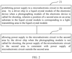
- the present application provides a driving method for an electronic device 200, which specifically comprises the following steps.
- Step S21 prohibiting power supply to a microelectronic circuit in the second area by a driver chip in a liquid crystal module of the electronic device when a photographing module of the electronic device is called for shooting, wherein a position of a second area on an array substrate in the liquid crystal module is corresponding to a light-transmitting area in the liquid crystal module.
- the photographing module when the photographing module is called for shooting, voltages on an upper side and a lower side of the liquid crystal molecules at positions corresponding to the light-transmitting area of the liquid crystal layer of the liquid crystal module are measured, and the voltages are zero. Liquid crystal molecules do not twist, which facilitates a light input amount of the photographing module 30 and improves a quality of an image during shooting.
- Step S22 allowing power supply to the microelectronic circuit in the second area by the driver chip when the photographing module is not called for shooting, the power supply of the microelectronic circuit in the second area is consistent with power supply of microelectronic circuit outside the second area.
- the voltages on the upper side and the lower side of the liquid crystal molecules at the positions of the liquid crystal layer corresponding to the light-transmitting area are measured, and the voltages are not equal to zero. At this time, the liquid crystal molecules are twisted, which facilitates display effect of the electronic device when not shooting.
- the embodiment of the present application provides a storage medium in which a plurality of instructions are stored, and the instructions can be loaded by the processor to execute steps in any driving method for the electronic device provided by the embodiment of the present application.
- the storage medium may comprise: read-only memory (ROM), random-access memory (RAM), magnetic disk, or optical disk, and so on.
- the electronic device 300 may be a device such as a smartphone, a tablet computer, or the like.
- the electronic device also comprises following components.
- An RF circuit 310 is used for receiving and sending electromagnetic waves to realize mutual conversion between electromagnetic waves and electrical signals, so as to communicate with a communication network or other devices.
- the RF circuit 310 may comprise various existing circuit elements for performing these functions, for example, antennas, radio frequency transceivers, digital signal processors, encryption/decryption chips, subscriber identity module (SIM) cards, memory, and the like.
- the RF circuit 310 may communicate with various networks such as the Internet, an intranet, a wireless network, or with other devices over a wireless network.
- the aforementioned wireless network may comprise a cellular telephone network, a wireless local area network, or a metropolitan area network.
- the aforementioned wireless network can use various communication standards, protocols, and technologies, comprising but not limited to Global System for Mobile Communication (GSM), Enhanced Data GSM Environment (EDGE), Wideband Code Division Multiple Access (WCDMA), Code Division Multiple Access (CDMA), Time Division Multiple Access (TDMA), Wireless Fidelity (Wi-Fi) (such as IEEE 802.11a, IEEE 802.11b, IEEE802.11g and/or IEEE 802.11n), Voice over Internet Protocol (VoIP), Worldwide Interoperability for Microwave Access (Wi-Max), other protocols for mail, instant messaging, short messaging, and any other suitable communication protocols, even those are not currently developed.
- GSM Global System for Mobile Communication
- EDGE Enhanced Data GSM Environment
- WCDMA Wideband Code Division Multiple Access
- CDMA Code Division Multiple Access
- TDMA Time Division Multiple Access
- Wi-Fi Wireless Fidelity
- IEEE 802.11a, IEEE 802.11b, IEEE802.11g and/or IEEE 802.11n such as IEEE 802.11a, IEEE 802.
- a memory 320 may be used to store software programs and modules, and a processor 380 executes various functional applications and data processing by running software programs and modules stored in the memory 320.
- the memory 320 may comprise high-speed random-access memory, and may also comprise non-volatile memory, such as one or more magnetic storage devices, flash memory, or other non-volatile solid-state memory.
- the memory 320 may further comprise memories located remotely from the processor 380, and these remote memories may be connected to the electronic device 300 through a network. Examples of such networks comprise, but are not limited to, the Internet, the intranet, the local area network, the mobile communication network, and combinations thereof.
- Input unit 330 may be used to receive input numerical or character information, and to generate signal inputs of keyboard, mouse, joystick, optical, or trackball related to user settings and function control.
- the input unit 330 may comprise a touch-sensitive surface 331 and other input devices 332.
- the touch-sensitive surface 331 also known as a touch display screen or touchpad, may collect touch operations thereon or nearby by a user (such as operations by the user to use fingers, stylus, and any suitable objects or accessories on or nearby the touch-sensitive surface 331) and drive corresponding connection devices according to a preset program.
- the touch-sensitive surface 331 may comprise two portions, a touch detection device and a touch controller.
- the touch detection device detects user's touch orientation and detects signals brought by the touch operations, and transmits the signals to the touch controller; the touch controller receives touch information from the touch detection device, and converts it into contact coordinates, and then sends it to the processor 380, and can receive commands sent by the processor 380 and execute it.
- the touch-sensitive surface 331 may be implemented using various types of resistive, capacitive, infrared, and surface acoustic waves.
- the input unit 330 may also comprise other input devices 332.
- the other input devices 332 may comprise, but are not limited to, one or more of physical keyboards, function keys (such as volume control keys, switch keys, etc.), trackballs, mice, joysticks, and the like.
- a display unit 340 may be used to display information input by or provided to the user and various graphical user interfaces of the electronic device 300, which may be consisted of graphics, text, icons, videos, and any combination thereof.
- the display unit 340 may comprise a display panel 341, optionally, the display panel 341 may be configured of a liquid crystal display (LCD), an organic light-emitting diode (OLED), and the like.
- the touch-sensitive surface 331 may cover the display panel 341, when the touch-sensitive surface 331 detects the touch operations thereon or nearby, and transmits it to the processor 380 to determine a type of a touch event, and then the processor 380 provides a corresponding visual output on the display panel 341 according to the type of the touch event.
- the touch-sensitive surface 331 and the display panel 341 are used as two separate components to realize input and output functions, in some embodiments, the touch-sensitive surface 331 and the display panel 341 may be integrated to realize the input and output functions.
- the electronic device 300 may also comprise at least one type of sensor 350, such as a light sensor, a motion sensor, and other sensors.
- the light sensor may comprise an ambient light sensor and a proximity sensor, wherein the ambient light sensor may adjust brightness of the display panel 341 according to brightness of ambient light rays, and the proximity sensor may turn off the display panel 341 and/or backlight when the electronic device 300 is moved near an ear.
- a gravitational acceleration sensor can detect magnitude of acceleration in all directions (usually three axes), and can detect the magnitude and direction of gravity when it is stationary, which can be used to recognize applications of mobile phone postures (such as horizontal and vertical screen switching, related games, magnetometer posture calibration), vibration recognition related functions (such as pedometer, tapping), and the like.
- mobile phone postures such as horizontal and vertical screen switching, related games, magnetometer posture calibration
- vibration recognition related functions such as pedometer, tapping
- sensors such as a gyroscope, a barometer, a hygrometer, a thermometer, an infrared sensor, etc., that can also be configured in the electronic device 300, details are not described here.
- An audio circuit 360, a speaker 361, and a microphone 362 may provide an audio interface between the user and the electronic device 300.
- the audio circuit 360 can transmit electrical signal converted from received audio data to the speaker 361, and the speaker 361 converts it into a sound signal and outputs it; on the other hand, the microphone 362 converts collected sound signal into an electrical signal, which is received by the audio circuit 360 and converted it into audio data, and then the audio data is processed by the output processor 380 and sent to, for example, another terminal through an antenna device 310, or the audio data is output to the memory 320 for further processing.
- the audio circuit 360 may also comprise a headphone jack to provide communication between a peripheral headphone and the electronic device 300.
- the processor 380 is a control center of the electronic device 300, and uses various interfaces and lines to connect various components of an entire mobile phone, by running or executing software programs and/or modules stored in the memory 320, and calling the data stored in the memory 320 to perform various functions of the electronic device 300 and process data, so as to monitor the mobile phone as a whole.
- the processor 380 may comprise one or more processing cores; in some embodiments, the processor 380 may integrate an application processor and a modem processor, wherein the application processor mainly handles an operating system, a user interface, and application programs, and so on, and the modem processor mainly deals with wireless communication. It can be understood that the above-mentioned modem processor may also not be integrated into the processor 380.
- the electronic device 300 also comprises a power source 390 (such as a battery) for powering supply to the various components.
- the power source may be logically connected to the processor 380 through a power management system to manage charging, discharging, power consumption management, and other functions through the power management system.
- the power source 390 may also comprise one or more DC or AC power sources, recharging systems, power failure detection circuits, power converters or inverters, power status indicators, and any other components.
- the electronic device 300 may further comprise a camera (e.g., a front-facing camera, a rear-facing camera), a BLUETOOTH module, and the like, which will not be repeated here.
- a camera e.g., a front-facing camera, a rear-facing camera
- BLUETOOTH module e.g., a BLUETOOTH module
- the above modules can be implemented as independent entities, or can be arbitrarily combined to be implemented as a same or several entities.
- the specific implementation of the above modules can refer to the previous method embodiments, which will not be repeated here.
- the thicknesses of the color resist and the black matrix in the first area, at the corresponding position of the light-transmitting area, of the color film substrate are smaller than the thicknesses of the color resist and the black matrix outside the first area, and the backlight module is provided with the through hole corresponding to the light-transmitting area, the photographing module is disposed corresponding to the through hole, so that external light rays can be obtained, thus under-screen photographing is achieved, and 100% full-screen design is satisfied.
Landscapes
- Physics & Mathematics (AREA)
- Engineering & Computer Science (AREA)
- Nonlinear Science (AREA)
- General Physics & Mathematics (AREA)
- Crystallography & Structural Chemistry (AREA)
- Chemical & Material Sciences (AREA)
- Computer Hardware Design (AREA)
- Mathematical Physics (AREA)
- Theoretical Computer Science (AREA)
- Optics & Photonics (AREA)
- Signal Processing (AREA)
- Multimedia (AREA)
- Human Computer Interaction (AREA)
- General Engineering & Computer Science (AREA)
- Devices For Indicating Variable Information By Combining Individual Elements (AREA)
- Liquid Crystal (AREA)
Abstract
Description
- The present application claims priority to
Chinese application No. 202010265472.5, filed on April 07, 2020 - The present application relates to a field of electronic equipment, and especially to an electronic device and a driving method therefor.
- In order to realize a selfie function, a front camera is always disposed on a screen, but if the front camera is disposed on the screen, it is impossible for a mobile phone to achieve 100% full screen ratio. Therefore, a full screen technology and a photography technology including the front camera are main driving forces of technology competition of mobile phone manufacturers at present stage. Generally speaking, the larger a ratio of a display area of a mobile phone screen to a front of the whole mobile phone is, the better a performance of the front camera, and more popular the mobile phone is with consumers. However, due to a functional difference between the front camera and a display screen, presence of the front camera will occupy a part of a front area of the mobile phone, which reduces the display area, that is, the screen ratio of the mobile phone is reduced. Regarding this issue, a solution is to hide the front camera inside the mobile phone itself through a lifting mechanical structure to avoid the front camera from occupying the display area. Another solution is that the mobile phone is set as a sliding cover, and the front camera is placed on a behind half of the mobile phone, which can also avoid the front camera from occupying the front area of the mobile phone.
- However, both the above two solutions to increase the screen ratio of the mobile phone have some disadvantages. For example, the front camera is set to the lifting structure, that is, it pops up when it is in use, and is stored in a cabin of the mobile phone when it is not in use. However, such mobile phone has a complex structure, high processing difficulty, high manufacturing cost, low reliability of an action of the front camera, and problems of frequent popping up easily lead to bumping damage to the front camera. The sliding type will lead to an increase in a thickness and volume of the mobile phone. In addition, the above two solutions cause a large gap on the mobile phone, water and dust can easily enter the gap, thereby affecting quality of the mobile phone.
- Embodiments of the present application provide an electronic device and a driving method therefor, so as to solve a problem that a 100% full screen cannot be realized.
- According to a first aspect of the present application, the present application provides an electronic device, comprises: a liquid crystal module, having a light-transmitting area, the liquid crystal module comprising an upper polarizer, a color film substrate, a liquid crystal layer, an array substrate, and a lower polarizer from a top to a bottom in sequence, wherein thicknesses of color resist and a black matrix in a first area, at a corresponding position of the light-transmitting area, of the color film substrate are lower than thicknesses of color resist and a black matrix outside the first area, the thicknesses of the color resist and the black matrix of the first area is 10% to 60% of the thicknesses of the color resist and the black matrix outside the first area, a second area is disposed on the array substrate at a corresponding position of the light-transmitting area, and an area of the second area is smaller than an area of the first area and larger than an area of a through hole; a backlight module, disposed below the liquid crystal module, the backlight module is provided with the through hole corresponding to the light-transmitting area; and a photographing module, disposed below the backlight module, the photographing module is disposed corresponding to the through hole, so that external light rays can be obtained by means of the through hole and the light-transmitting area.
- Further, the area of the second area is determined by a shooting angle of the photographing module and a size of an exposed lens.
- Further, the area of the first area is determined by a shooting angle of the photographing module and a size of an exposed lens.
- Further, the area of the through hole is determined by a shooting angle of the photographing module and a size of an exposed lens.
- Further, the electronic device further comprises a driver chip, and the driver chip is configured to prohibit power supply to a microelectronic circuit in the second area when the photographing module of the electronic device is called for shooting.
- Further, the driver chip is further configured to allow power supply to the microelectronic circuit in the second area when the photographing module is not called for shooting, the power supply to the microelectronic circuit in the second area is consistent with power supply to microelectronic circuit outside the second area.
- According to a second aspect of the present application, the present application provides an electronic device, comprises: a liquid crystal module, having a light-transmitting area, the liquid crystal module comprising an upper polarizer, a color film substrate, a liquid crystal layer, an array substrate, and a lower polarizer from a top to a bottom in sequence, wherein thicknesses of color resist and a black matrix in a first area, at a corresponding position of the light-transmitting area, of the color film substrate are lower than thicknesses of color resist and a black matrix outside the first area; a backlight module, disposed below the liquid crystal module, the backlight module is provided with a through hole corresponding to the light-transmitting area; and a photographing module, disposed below the backlight module, the photographing module is disposed corresponding to the through hole, so that external light rays can be obtained by means of the through hole and the light-transmitting area.
- Further, a second area is disposed on the array substrate at a corresponding position of the light-transmitting area, and an area of the second area is smaller than an area of the first area and larger than an area of the through hole.
- Further, the area of the second area is determined by a shooting angle of the photographing module and a size of an exposed lens.
- Further, the area of the first area is determined by a shooting angle of the photographing module and a size of an exposed lens.
- Further, the area of the through hole is determined by a shooting angle of the photographing module and a size of an exposed lens.
- Further, the thicknesses of the color resist and the black matrix of the first area is 10% to 60% of the thicknesses of the color resist and the black matrix outside the first area.
- Further, the electronic device further comprises a driver chip, and the driver chip is configured to prohibit power supply to a microelectronic circuit in the second area when the photographing module of the electronic device is called for shooting.
- Further, the driver chip is further configured to allow power supply to the microelectronic circuit in the second area when the photographing module is not called for shooting, the power supply to the microelectronic circuit in the second area is consistent with power supply to microelectronic circuit outside the second area.
- According to a third aspect of the present application, the present application provides a driving method using the above-mentioned electronic device, the method comprises: prohibiting power supply to a microelectronic circuit in a second area by a driver chip in the liquid crystal module of the electronic device when the photographing module of the electronic device is called for shooting, wherein a position of the second area on the array substrate in the liquid crystal module is corresponding to the light-transmitting area in the liquid crystal module; and allowing power supply to the microelectronic circuit in the second area by the driver chip when the photographing module is not called for shooting, the power supply to the microelectronic circuit in the second area is consistent with power supply to microelectronic circuit outside the second area.
- Further, measuring voltages on an upper side and a lower side of the liquid crystal molecules at positions of the liquid crystal layer in the liquid crystal module corresponding to the light-transmitting area when the photographing module is called for shooting, and obtain that the voltages are zero; and measuring the voltages on the upper side and the lower side of the liquid crystal molecules at the positions of the liquid crystal layer corresponding to the light-transmitting area when the photographing module is not called for shooting, and obtain that the voltages are not equal to zero.
- Compared with an existing technology, the electronic device and the driving method therefor provided by the present application, the thicknesses of the color resist and the black matrix in the first area, at the corresponding position of a light-transmitting area, of the color film substrate are smaller than the thicknesses of the color resist and the black matrix outside the first area, and the backlight module is provided with the through hole corresponding to the light-transmitting area, the photographing module is disposed corresponding to the through hole, so that the external light rays can be obtained, thus under-screen photographing is achieved, and 100% full-screen design is satisfied.
-
-
FIG. 1 is a schematic structural diagram of an electronic device provided by an embodiment of the present application. -
FIG. 2 is a schematic flowchart of steps of a driving method for the electronic device provided by an embodiment of the present application. -
FIG. 3 is a specific schematic structure diagram of the electronic device provided by an embodiment of the present application. - Technical solutions in embodiments of the present application will be clearly and completely described below with reference to the accompanying drawings in the embodiments of the present application. Obviously, the described embodiments are only parts of the embodiments of the present application, but not all of the embodiments. Based on the embodiments in the present application, all other embodiments obtained by those skilled in the art without creative work fall within protection scope of the present application.
- Terms "first", "second", "third", etc. (if exist) in the description and claims of the present application and the above-mentioned figures are used to distinguish similar objects and are not necessarily used to describe a particular order or sequence. It is to be understood that the objects as described are interchangeable under appropriate circumstances. Furthermore, terms "comprising" and "having", and any variations thereof, are intended to cover non-exclusive inclusion.
- In the detailed description, the drawings discussed below and the embodiments used to describe the principles of the present disclosure are by way of illustration only and should not be construed as limiting the scope of the present disclosure. Those skilled in the art will understand that the principles of the present application may be implemented in any suitably arranged system. Exemplary embodiments will be described in detail, examples of which are illustrated in the accompanying drawings. Also, a terminal according to an exemplary embodiment will be described in detail with reference to the accompanying drawings. The same reference numbers in the figures refer to the same elements. The same reference numbers in the figures refer to the same elements.
- The terms used in this detailed description are used to describe a particular embodiment only, and are not intended to convey the concepts of the present application. Expressions used in the singular cover expressions in the plural unless the context clearly indicates a different meaning. In the specification of the present application, it should be understood that terms such as "comprising", "having" and "containing" are intended to indicate the existence of the possibility of the features, numbers, steps, actions or combinations thereof disclosed in the specification of the present application, and are not intended to be the possibility that one or more other features, numbers, steps, actions, or combinations thereof may be present or may be added is excluded. The same reference numbers in the drawings refer to the same parts.
- As shown in
FIG. 1 , the present application provides an electronic device 100, which is applied to the electronic device, comprising: aliquid crystal module 10, anupper polarizer 101, acolor filter substrate 102, aliquid crystal layer 103, anarray substrate 104, a lower polarizer 105, a light-transmitting area 110, afirst area 120, asecond area 130, abacklight module 20, a throughhole 210, and aphotographing module 30. - The
liquid crystal module 10 is provided with the light-transmittingarea 110. Theliquid crystal module 10 comprises theupper polarizer 101, thecolor filter substrate 102, theliquid crystal layer 103, thearray substrate 104, and the lower polarizer 105 from a top to a bottom in sequence. - In an embodiment of the present application, the
color filter substrate 102 is provided with thefirst area 120 at a position corresponding to the light-transmittingarea 110, and an area of thefirst area 120 is determined by a shooting angle of thephotographing module 30 and a size of an exposed lens. Wherein thicknesses of color resist and a black matrix in thefirst area 120 are lower than thicknesses of color resist and a black matrix outside the first area; specifically, the thicknesses of the color resist and the black matrix of thefirst area 120 is 10% to 60% of the thicknesses of the color resist and the black matrix outside thefirst area 120, thus, light transmittance is increased, so that the photographing module obtains external light rays when shooting, and an image is clearer. - In the embodiment of the present application, the
second area 130 is disposed on thearray substrate 104 at a corresponding position of the light-transmittingarea 110, an area of thesecond area 130 is determined by the shooting angle of thephotographing module 30 and the size of the exposed lens. Microelectronic circuits in thesecond area 130 are individually controlled by a driver chip. Specifically, the driver chip is configured to prohibit power supply to the microelectronic circuit in thesecond area 130 when the photographing module of the electronic device is called for shooting. At this time, voltages on an upper side and a lower side of liquid crystal molecules at positions corresponding to the light-transmittingarea 110 of theliquid crystal layer 103 are zero. The liquid crystal molecules do not twist, which facilitates a light input amount of the photographingmodule 30 and improves a quality of the image during shooting. The driver chip is also used to allow power supply to the microelectronic circuit in thesecond area 130 when the photographingmodule 30 is not called for shooting, the power supply of the microelectronic circuit in thesecond area 130 is consistent with power supply of microelectronic circuit outside the second area. At this time, the voltages on the upper side and the lower side of the liquid crystal molecules at positions corresponding to the light-transmittingarea 110 of theliquid crystal layer 103 are not zero, and the liquid crystal molecules are twisted, which facilitates display effect of the electronic device when not shooting. - The
backlight module 20 is disposed below theliquid crystal module 10. Thebacklight module 20 is defined with a throughhole 210 corresponding to the light-transmittingarea 110. An area of the throughhole 210 is determined by the shooting angle of the photographingmodule 30 and the size of the exposed lens. The throughhole 210 is used for the photographingmodule 30 to obtain external light rays. - The photographing
module 30 is disposed below thebacklight module 20. The photographingmodule 30 is disposed corresponding to the throughhole 210, so that external light rays can be obtained by means of the throughhole 210 and the light-transmittingarea 110. According to a position arrangement of the photographingmodule 30 of the present application, the photographingmodule 30 is disposed under the display screen to achieve 100% full-screen display, and due to arrangements of the backlight module and the liquid crystal module, when the photographing module is called for shooting, there is enough light rays to make the image clear. - In the present application, the thicknesses of the color resist and the black matrix in the first area, at the corresponding position of the light-transmitting area, of the color film substrate are smaller than the thicknesses of the color resist and the black matrix outside the first area, and the backlight module is defined with the through hole corresponding to the light-transmitting area, the photographing module is disposed corresponding to the through hole, so that external light rays can be obtained, thus under-screen photographing is achieved, and 100% full-screen design is satisfied.
- As shown in
FIG. 2 , the present application provides a driving method for an electronic device 200, which specifically comprises the following steps. - Step S21, prohibiting power supply to a microelectronic circuit in the second area by a driver chip in a liquid crystal module of the electronic device when a photographing module of the electronic device is called for shooting, wherein a position of a second area on an array substrate in the liquid crystal module is corresponding to a light-transmitting area in the liquid crystal module.
- In the embodiment of the present application, when the photographing module is called for shooting, voltages on an upper side and a lower side of the liquid crystal molecules at positions corresponding to the light-transmitting area of the liquid crystal layer of the liquid crystal module are measured, and the voltages are zero. Liquid crystal molecules do not twist, which facilitates a light input amount of the photographing
module 30 and improves a quality of an image during shooting. - Step S22, allowing power supply to the microelectronic circuit in the second area by the driver chip when the photographing module is not called for shooting, the power supply of the microelectronic circuit in the second area is consistent with power supply of microelectronic circuit outside the second area.
- In the embodiment of the present application, when the photographing module is not called for shooting, the voltages on the upper side and the lower side of the liquid crystal molecules at the positions of the liquid crystal layer corresponding to the light-transmitting area are measured, and the voltages are not equal to zero. At this time, the liquid crystal molecules are twisted, which facilitates display effect of the electronic device when not shooting.
- Those of ordinary skill in the art can understand that all or part of the steps in the various methods of the above embodiment can be completed by instructions, or completed by instructions that control relevant hardware, and the instructions can be stored in a computer-readable storage medium, and is loaded and executed by a processor. Therefore, the embodiment of the present application provides a storage medium in which a plurality of instructions are stored, and the instructions can be loaded by the processor to execute steps in any driving method for the electronic device provided by the embodiment of the present application.
- Wherein, the storage medium may comprise: read-only memory (ROM), random-access memory (RAM), magnetic disk, or optical disk, and so on.
- As shown in
FIG. 3 , it is a specific structure of anelectronic device 300 provided in an embodiment of the present application, theelectronic device 300 may be a device such as a smartphone, a tablet computer, or the like. The electronic device also comprises following components. - An
RF circuit 310 is used for receiving and sending electromagnetic waves to realize mutual conversion between electromagnetic waves and electrical signals, so as to communicate with a communication network or other devices. TheRF circuit 310 may comprise various existing circuit elements for performing these functions, for example, antennas, radio frequency transceivers, digital signal processors, encryption/decryption chips, subscriber identity module (SIM) cards, memory, and the like. TheRF circuit 310 may communicate with various networks such as the Internet, an intranet, a wireless network, or with other devices over a wireless network. The aforementioned wireless network may comprise a cellular telephone network, a wireless local area network, or a metropolitan area network. The aforementioned wireless network can use various communication standards, protocols, and technologies, comprising but not limited to Global System for Mobile Communication (GSM), Enhanced Data GSM Environment (EDGE), Wideband Code Division Multiple Access (WCDMA), Code Division Multiple Access (CDMA), Time Division Multiple Access (TDMA), Wireless Fidelity (Wi-Fi) (such as IEEE 802.11a, IEEE 802.11b, IEEE802.11g and/or IEEE 802.11n), Voice over Internet Protocol (VoIP), Worldwide Interoperability for Microwave Access (Wi-Max), other protocols for mail, instant messaging, short messaging, and any other suitable communication protocols, even those are not currently developed. - A
memory 320 may be used to store software programs and modules, and aprocessor 380 executes various functional applications and data processing by running software programs and modules stored in thememory 320. Thememory 320 may comprise high-speed random-access memory, and may also comprise non-volatile memory, such as one or more magnetic storage devices, flash memory, or other non-volatile solid-state memory. In some embodiments, thememory 320 may further comprise memories located remotely from theprocessor 380, and these remote memories may be connected to theelectronic device 300 through a network. Examples of such networks comprise, but are not limited to, the Internet, the intranet, the local area network, the mobile communication network, and combinations thereof. -
Input unit 330 may be used to receive input numerical or character information, and to generate signal inputs of keyboard, mouse, joystick, optical, or trackball related to user settings and function control. Specifically, theinput unit 330 may comprise a touch-sensitive surface 331 andother input devices 332. The touch-sensitive surface 331, also known as a touch display screen or touchpad, may collect touch operations thereon or nearby by a user (such as operations by the user to use fingers, stylus, and any suitable objects or accessories on or nearby the touch-sensitive surface 331) and drive corresponding connection devices according to a preset program. Optionally, the touch-sensitive surface 331 may comprise two portions, a touch detection device and a touch controller. Wherein, the touch detection device detects user's touch orientation and detects signals brought by the touch operations, and transmits the signals to the touch controller; the touch controller receives touch information from the touch detection device, and converts it into contact coordinates, and then sends it to theprocessor 380, and can receive commands sent by theprocessor 380 and execute it. In addition, the touch-sensitive surface 331 may be implemented using various types of resistive, capacitive, infrared, and surface acoustic waves. Apart from the touch-sensitive surface 331, theinput unit 330 may also compriseother input devices 332. Specifically, theother input devices 332 may comprise, but are not limited to, one or more of physical keyboards, function keys (such as volume control keys, switch keys, etc.), trackballs, mice, joysticks, and the like. - A
display unit 340 may be used to display information input by or provided to the user and various graphical user interfaces of theelectronic device 300, which may be consisted of graphics, text, icons, videos, and any combination thereof. Thedisplay unit 340 may comprise adisplay panel 341, optionally, thedisplay panel 341 may be configured of a liquid crystal display (LCD), an organic light-emitting diode (OLED), and the like. Further, the touch-sensitive surface 331 may cover thedisplay panel 341, when the touch-sensitive surface 331 detects the touch operations thereon or nearby, and transmits it to theprocessor 380 to determine a type of a touch event, and then theprocessor 380 provides a corresponding visual output on thedisplay panel 341 according to the type of the touch event. InFIG. 3 , although the touch-sensitive surface 331 and thedisplay panel 341 are used as two separate components to realize input and output functions, in some embodiments, the touch-sensitive surface 331 and thedisplay panel 341 may be integrated to realize the input and output functions. - The
electronic device 300 may also comprise at least one type ofsensor 350, such as a light sensor, a motion sensor, and other sensors. Specifically, the light sensor may comprise an ambient light sensor and a proximity sensor, wherein the ambient light sensor may adjust brightness of thedisplay panel 341 according to brightness of ambient light rays, and the proximity sensor may turn off thedisplay panel 341 and/or backlight when theelectronic device 300 is moved near an ear. As a type of motion sensor, a gravitational acceleration sensor can detect magnitude of acceleration in all directions (usually three axes), and can detect the magnitude and direction of gravity when it is stationary, which can be used to recognize applications of mobile phone postures (such as horizontal and vertical screen switching, related games, magnetometer posture calibration), vibration recognition related functions (such as pedometer, tapping), and the like. As for other sensors, such as a gyroscope, a barometer, a hygrometer, a thermometer, an infrared sensor, etc., that can also be configured in theelectronic device 300, details are not described here. - An
audio circuit 360, aspeaker 361, and amicrophone 362 may provide an audio interface between the user and theelectronic device 300. Theaudio circuit 360 can transmit electrical signal converted from received audio data to thespeaker 361, and thespeaker 361 converts it into a sound signal and outputs it; on the other hand, themicrophone 362 converts collected sound signal into an electrical signal, which is received by theaudio circuit 360 and converted it into audio data, and then the audio data is processed by theoutput processor 380 and sent to, for example, another terminal through anantenna device 310, or the audio data is output to thememory 320 for further processing. Theaudio circuit 360 may also comprise a headphone jack to provide communication between a peripheral headphone and theelectronic device 300. - The
processor 380 is a control center of theelectronic device 300, and uses various interfaces and lines to connect various components of an entire mobile phone, by running or executing software programs and/or modules stored in thememory 320, and calling the data stored in thememory 320 to perform various functions of theelectronic device 300 and process data, so as to monitor the mobile phone as a whole. Optionally, theprocessor 380 may comprise one or more processing cores; in some embodiments, theprocessor 380 may integrate an application processor and a modem processor, wherein the application processor mainly handles an operating system, a user interface, and application programs, and so on, and the modem processor mainly deals with wireless communication. It can be understood that the above-mentioned modem processor may also not be integrated into theprocessor 380. - The
electronic device 300 also comprises a power source 390 (such as a battery) for powering supply to the various components. In some embodiments, the power source may be logically connected to theprocessor 380 through a power management system to manage charging, discharging, power consumption management, and other functions through the power management system. Thepower source 390 may also comprise one or more DC or AC power sources, recharging systems, power failure detection circuits, power converters or inverters, power status indicators, and any other components. - Although not shown, the
electronic device 300 may further comprise a camera (e.g., a front-facing camera, a rear-facing camera), a BLUETOOTH module, and the like, which will not be repeated here. - During specific implementation, the above modules can be implemented as independent entities, or can be arbitrarily combined to be implemented as a same or several entities. The specific implementation of the above modules can refer to the previous method embodiments, which will not be repeated here.
- In the present application, the thicknesses of the color resist and the black matrix in the first area, at the corresponding position of the light-transmitting area, of the color film substrate are smaller than the thicknesses of the color resist and the black matrix outside the first area, and the backlight module is provided with the through hole corresponding to the light-transmitting area, the photographing module is disposed corresponding to the through hole, so that external light rays can be obtained, thus under-screen photographing is achieved, and 100% full-screen design is satisfied.
- The electronic device and the driving method therefor provided by the embodiments of the present application have been described in detail above. The principles and implementations of the present application are described with specific examples. The method of the application and its core idea; at the same time, for those skilled in the art, according to the idea of the present application, there will be changed in the specific embodiments and application scope. In summary, the content of this specification should not be construed as a limitation to the present application.
Claims (16)
- An electronic device, comprising:a liquid crystal module, having a light-transmitting area, the liquid crystal module comprising an upper polarizer, a color film substrate, a liquid crystal layer, an array substrate, and a lower polarizer from a top to a bottom in sequence, wherein thicknesses of color resist and a black matrix in a first area, at a corresponding position of the light-transmitting area, of the color film substrate are lower than thicknesses of color resist and a black matrix outside the first area, the thicknesses of the color resist and the black matrix of the first area is 10% to 60% of the thicknesses of the color resist and the black matrix outside the first area, a second area is disposed on the array substrate at a corresponding position of the light-transmitting area, and an area of the second area is smaller than that of the first area and larger than an area of a through hole;a backlight module, disposed below the liquid crystal module, the backlight module is defined with the through hole corresponding to the light-transmitting area; anda photographing module, disposed below the backlight module, the photographing module is disposed corresponding to the through hole, so that external light rays can be obtained by means of the through hole and the light-transmitting area.
- The electronic device as claimed in claim 1, wherein the area of the second area is determined by a shooting angle of the photographing module and a size of an exposed lens.
- The electronic device as claimed in claim 1, wherein the area of the first area is determined by a shooting angle of the photographing module and a size of an exposed lens.
- The electronic device as claimed in claim 1, wherein the area of the through hole is determined by a shooting angle of the photographing module and a size of an exposed lens.
- The electronic device as claimed in claim 1, wherein the electronic device further comprises a driver chip, and the driver chip is configured to prohibit power supply to a microelectronic circuit in the second area when the photographing module of the electronic device is called for shooting.
- The electronic device as claimed in claim 5, wherein the driver chip is further configured to allow power supply to the microelectronic circuit in the second area when the photographing module is not called for shooting, the power supply to the microelectronic circuit in the second area is consistent with power supply to microelectronic circuit outside the second area.
- An electronic device, comprising:a liquid crystal module, having a light-transmitting area, the liquid crystal module comprising an upper polarizer, a color film substrate, a liquid crystal layer, an array substrate, and a lower polarizer from a top to a bottom in sequence, wherein thicknesses of color resist and a black matrix in a first area, at a corresponding position of the light-transmitting area, of the color film substrate are lower than thicknesses of color resist and a black matrix outside the first area;a backlight module, disposed below the liquid crystal module, the backlight module is provided with a through hole corresponding to the light-transmitting area; anda photographing module, disposed below the backlight module, the photographing module is disposed corresponding to the through hole, so that external light rays can be obtained by means of the through hole and the light-transmitting area.
- The electronic device as claimed in claim 7, wherein a second area is disposed on the array substrate at a corresponding position of the light-transmitting area, and an area of the second area is smaller than an area of the first area and larger than an area of the through hole.
- The electronic device as claimed in claim 8, wherein the area of the second area is determined by a shooting angle of the photographing module and a size of an exposed lens.
- The electronic device as claimed in claim 7, wherein the area of the first area is determined by a shooting angle of the photographing module and a size of an exposed lens.
- The electronic device as claimed in claim 7, wherein the area of the through hole is determined by a shooting angle of the photographing module and a size of an exposed lens.
- The electronic device as claimed in claim 7, wherein the thicknesses of the color resist and the black matrix of the first area is 10% to 60% of the thicknesses of the color resist and the black matrix outside the first area.
- The electronic device as claimed in claim 8, wherein the electronic device further comprises a driver chip, and the driver chip is configured to prohibit power supply to a microelectronic circuit in the second area when the photographing module of the electronic device is called for shooting.
- The electronic device as claimed in claim 13, wherein the driver chip is further configured to allow power supply to the microelectronic circuit in the second area when the photographing module is not called for shooting, the power supply to the microelectronic circuit in the second area is consistent with power supply to microelectronic circuit outside the second area.
- A driving method for the electronic device as claimed in claim 7, comprising:prohibiting power supply to a microelectronic circuit in a second area by a driver chip in the liquid crystal module of the electronic device when the photographing module of the electronic device is called for shooting, wherein a position of the second area on the array substrate in the liquid crystal module is corresponding to the light-transmitting area in the liquid crystal module; andallowing power supply to the microelectronic circuit in the second area by the driver chip when the photographing module is not called for shooting, the power supply to the microelectronic circuit in the second area is consistent with power supply to microelectronic circuit outside the second area.
- The driving method as claimed in claim 15, further comprising:measuring voltages on an upper side and a lower side of the liquid crystal molecules at positions of the liquid crystal layer in the liquid crystal module corresponding to the light-transmitting area when the photographing module is called for shooting, and obtain that the voltages are zero; andmeasuring the voltages on the upper side and the lower side of the liquid crystal molecules at the positions of the liquid crystal layer corresponding to the light-transmitting area when the photographing module is not called for shooting, and obtain that the voltages are not equal to zero.
Applications Claiming Priority (2)
| Application Number | Priority Date | Filing Date | Title |
|---|---|---|---|
| CN202010265472.5A CN111443518A (en) | 2020-04-07 | 2020-04-07 | Electronic device and driving method thereof |
| PCT/CN2020/089624 WO2021203512A1 (en) | 2020-04-07 | 2020-05-11 | Electronic device and driving method therefor |
Publications (3)
| Publication Number | Publication Date |
|---|---|
| EP4134732A1 true EP4134732A1 (en) | 2023-02-15 |
| EP4134732A4 EP4134732A4 (en) | 2024-05-01 |
| EP4134732B1 EP4134732B1 (en) | 2026-01-28 |
Family
ID=71651046
Family Applications (1)
| Application Number | Title | Priority Date | Filing Date |
|---|---|---|---|
| EP20930120.9A Active EP4134732B1 (en) | 2020-04-07 | 2020-05-11 | Electronic device and driving method therefor |
Country Status (4)
| Country | Link |
|---|---|
| US (1) | US11892723B2 (en) |
| EP (1) | EP4134732B1 (en) |
| CN (1) | CN111443518A (en) |
| WO (1) | WO2021203512A1 (en) |
Families Citing this family (2)
| Publication number | Priority date | Publication date | Assignee | Title |
|---|---|---|---|---|
| US11678042B2 (en) * | 2021-01-27 | 2023-06-13 | Qualcomm Incorporated | In-display camera activation |
| CN113777687B (en) | 2021-08-12 | 2023-04-18 | 惠州Tcl云创科技有限公司 | Camera assembly under screen, backlight module and display device |
Family Cites Families (12)
| Publication number | Priority date | Publication date | Assignee | Title |
|---|---|---|---|---|
| JP4728793B2 (en) * | 2005-12-14 | 2011-07-20 | 株式会社アイ・オー・データ機器 | Display device and control method thereof |
| KR20130021160A (en) * | 2011-08-22 | 2013-03-05 | 삼성디스플레이 주식회사 | Display apparatus and method for manufacturing the same |
| US9733509B2 (en) * | 2015-08-06 | 2017-08-15 | Chunghwa Picture Tubes, Ltd. | LCD display panel and color filter substrate |
| KR102342609B1 (en) * | 2017-04-25 | 2021-12-22 | 후아웨이 테크놀러지 컴퍼니 리미티드 | Lcd display screen, electronic device, manufacturing method for lcd display screen |
| CN110888261A (en) * | 2018-12-07 | 2020-03-17 | 鸿富锦精密工业(深圳)有限公司 | Display panel and display device |
| CN210605285U (en) * | 2019-03-26 | 2020-05-22 | 武汉华星光电技术有限公司 | Display panel and display device |
| CN110010666B (en) * | 2019-03-28 | 2021-03-16 | 武汉华星光电半导体显示技术有限公司 | Under-screen camera structure of OLED screen and OLED screen |
| CN109856850B (en) * | 2019-03-29 | 2020-10-13 | 武汉华星光电技术有限公司 | Display device |
| CN110471211B (en) * | 2019-08-28 | 2024-08-30 | 武汉华星光电技术有限公司 | Liquid crystal display panel, liquid crystal display device and electronic equipment |
| CN110579898A (en) * | 2019-09-23 | 2019-12-17 | 武汉华星光电技术有限公司 | display module and dispensing method thereof |
| CN110716340A (en) * | 2019-09-23 | 2020-01-21 | 武汉华星光电技术有限公司 | Display device, electronic equipment and manufacturing method of display device |
| CN110676301B (en) * | 2019-10-30 | 2022-04-15 | 武汉天马微电子有限公司 | Organic light-emitting display panel and display device |
-
2020
- 2020-04-07 CN CN202010265472.5A patent/CN111443518A/en active Pending
- 2020-05-11 US US17/995,257 patent/US11892723B2/en active Active
- 2020-05-11 EP EP20930120.9A patent/EP4134732B1/en active Active
- 2020-05-11 WO PCT/CN2020/089624 patent/WO2021203512A1/en not_active Ceased
Also Published As
| Publication number | Publication date |
|---|---|
| EP4134732A4 (en) | 2024-05-01 |
| WO2021203512A1 (en) | 2021-10-14 |
| EP4134732B1 (en) | 2026-01-28 |
| US20230176415A1 (en) | 2023-06-08 |
| CN111443518A (en) | 2020-07-24 |
| US11892723B2 (en) | 2024-02-06 |
Similar Documents
| Publication | Publication Date | Title |
|---|---|---|
| US11366563B2 (en) | Electronic device and method for inducing input | |
| CN105518605B (en) | A touch operation method and device for a terminal | |
| CN108521499B (en) | Antenna switching method, storage medium and electronic device | |
| US12307271B2 (en) | Electronic device and multi-window control method of electronic device | |
| CN108494957A (en) | Antenna switching method and device, storage medium and electronic equipment | |
| CN106484283A (en) | A display control method and mobile terminal | |
| CN106534550B (en) | Text information reading method and mobile terminal | |
| US20220319378A1 (en) | Screen color temperature control method, apparatus, storage medium, and mobile terminal | |
| CN107609439A (en) | Method, device, storage medium and terminal for processing radio frequency interference | |
| US20200150860A1 (en) | Mobile terminal and control method therefor, and readable storage medium | |
| CN108418969B (en) | Antenna feed point switching method and device, storage medium and electronic equipment | |
| CN105141854A (en) | Flash control method, device and terminal equipment | |
| US11262911B2 (en) | Integrated home key and virtual key area for a smart terminal | |
| CN106055947A (en) | Method, device and mobile terminal for unlocking mobile terminal by fingerprint | |
| WO2022082960A1 (en) | Local display region compensation value determination method, apparatus, storage medium and terminal device | |
| US11892723B2 (en) | Electronic device and driving method therefor | |
| CN105792299A (en) | Optimal use method, device and mobile terminal of 3G network | |
| CN111368238A (en) | Status bar adjustment method, device, mobile terminal and storage medium | |
| CN106210514A (en) | Method, device and smart device for taking pictures and focusing | |
| CN105718141A (en) | Method for moving desktop icons and mobile terminal | |
| CN110740265A (en) | Image processing method and terminal equipment | |
| CN110312274A (en) | A kind of method for building up and electronic equipment of wireless access point | |
| KR102940208B1 (en) | Electronic device and method for driving slide based on multi touch | |
| WO2023138214A1 (en) | Screen matching method, screen configuration method, and screen matching device | |
| CN111917982A (en) | Camera selection method and device, storage medium and mobile terminal |
Legal Events
| Date | Code | Title | Description |
|---|---|---|---|
| STAA | Information on the status of an ep patent application or granted ep patent |
Free format text: STATUS: THE INTERNATIONAL PUBLICATION HAS BEEN MADE |
|
| PUAI | Public reference made under article 153(3) epc to a published international application that has entered the european phase |
Free format text: ORIGINAL CODE: 0009012 |
|
| STAA | Information on the status of an ep patent application or granted ep patent |
Free format text: STATUS: REQUEST FOR EXAMINATION WAS MADE |
|
| 17P | Request for examination filed |
Effective date: 20221103 |
|
| AK | Designated contracting states |
Kind code of ref document: A1 Designated state(s): AL AT BE BG CH CY CZ DE DK EE ES FI FR GB GR HR HU IE IS IT LI LT LU LV MC MK MT NL NO PL PT RO RS SE SI SK SM TR |
|
| DAV | Request for validation of the european patent (deleted) | ||
| DAX | Request for extension of the european patent (deleted) | ||
| A4 | Supplementary search report drawn up and despatched |
Effective date: 20240402 |
|
| RIC1 | Information provided on ipc code assigned before grant |
Ipc: H04N 23/57 20230101ALI20240325BHEP Ipc: G06F 1/16 20060101ALI20240325BHEP Ipc: G02F 1/1333 20060101ALI20240325BHEP Ipc: H04M 1/02 20060101ALI20240325BHEP Ipc: G09G 3/36 20060101ALI20240325BHEP Ipc: G02F 1/1335 20060101AFI20240325BHEP |
|
| STAA | Information on the status of an ep patent application or granted ep patent |
Free format text: STATUS: EXAMINATION IS IN PROGRESS |
|
| 17Q | First examination report despatched |
Effective date: 20250325 |
|
| GRAP | Despatch of communication of intention to grant a patent |
Free format text: ORIGINAL CODE: EPIDOSNIGR1 |
|
| STAA | Information on the status of an ep patent application or granted ep patent |
Free format text: STATUS: GRANT OF PATENT IS INTENDED |
|
| INTG | Intention to grant announced |
Effective date: 20251020 |
|
| GRAS | Grant fee paid |
Free format text: ORIGINAL CODE: EPIDOSNIGR3 |
|
| GRAA | (expected) grant |
Free format text: ORIGINAL CODE: 0009210 |
|
| STAA | Information on the status of an ep patent application or granted ep patent |
Free format text: STATUS: THE PATENT HAS BEEN GRANTED |
|
| P01 | Opt-out of the competence of the unified patent court (upc) registered |
Free format text: CASE NUMBER: UPC_APP_0014499_4134732/2025 Effective date: 20251124 |
|
| AK | Designated contracting states |
Kind code of ref document: B1 Designated state(s): AL AT BE BG CH CY CZ DE DK EE ES FI FR GB GR HR HU IE IS IT LI LT LU LV MC MK MT NL NO PL PT RO RS SE SI SK SM TR |
|
| REG | Reference to a national code |
Ref country code: CH Ref legal event code: F10 Free format text: ST27 STATUS EVENT CODE: U-0-0-F10-F00 (AS PROVIDED BY THE NATIONAL OFFICE) Effective date: 20260128 Ref country code: GB Ref legal event code: FG4D |
|
| REG | Reference to a national code |
Ref country code: DE Ref legal event code: R096 Ref document number: 602020066389 Country of ref document: DE |
|
| REG | Reference to a national code |
Ref country code: IE Ref legal event code: FG4D |
|
| PGFP | Annual fee paid to national office [announced via postgrant information from national office to epo] |
Ref country code: GB Payment date: 20260306 Year of fee payment: 7 |