EP4133118B1 - Method for monitoring process conditions of, and method for controlling, a plasma pvd process - Google Patents
Method for monitoring process conditions of, and method for controlling, a plasma pvd process Download PDFInfo
- Publication number
- EP4133118B1 EP4133118B1 EP21716868.1A EP21716868A EP4133118B1 EP 4133118 B1 EP4133118 B1 EP 4133118B1 EP 21716868 A EP21716868 A EP 21716868A EP 4133118 B1 EP4133118 B1 EP 4133118B1
- Authority
- EP
- European Patent Office
- Prior art keywords
- plasma
- target
- radio frequency
- power supply
- response
- Prior art date
- Legal status (The legal status is an assumption and is not a legal conclusion. Google has not performed a legal analysis and makes no representation as to the accuracy of the status listed.)
- Active
Links
Images



Classifications
-
- H—ELECTRICITY
- H05—ELECTRIC TECHNIQUES NOT OTHERWISE PROVIDED FOR
- H05H—PLASMA TECHNIQUE; PRODUCTION OF ACCELERATED ELECTRICALLY-CHARGED PARTICLES OR OF NEUTRONS; PRODUCTION OR ACCELERATION OF NEUTRAL MOLECULAR OR ATOMIC BEAMS
- H05H1/00—Generating plasma; Handling plasma
-
- C—CHEMISTRY; METALLURGY
- C23—COATING METALLIC MATERIAL; COATING MATERIAL WITH METALLIC MATERIAL; CHEMICAL SURFACE TREATMENT; DIFFUSION TREATMENT OF METALLIC MATERIAL; COATING BY VACUUM EVAPORATION, BY SPUTTERING, BY ION IMPLANTATION OR BY CHEMICAL VAPOUR DEPOSITION, IN GENERAL; INHIBITING CORROSION OF METALLIC MATERIAL OR INCRUSTATION IN GENERAL
- C23C—COATING METALLIC MATERIAL; COATING MATERIAL WITH METALLIC MATERIAL; SURFACE TREATMENT OF METALLIC MATERIAL BY DIFFUSION INTO THE SURFACE, BY CHEMICAL CONVERSION OR SUBSTITUTION; COATING BY VACUUM EVAPORATION, BY SPUTTERING, BY ION IMPLANTATION OR BY CHEMICAL VAPOUR DEPOSITION, IN GENERAL
- C23C14/00—Coating by vacuum evaporation, by sputtering or by ion implantation of the coating forming material
- C23C14/22—Coating by vacuum evaporation, by sputtering or by ion implantation of the coating forming material characterised by the process of coating
- C23C14/34—Sputtering
- C23C14/35—Sputtering by application of a magnetic field, e.g. magnetron sputtering
-
- C—CHEMISTRY; METALLURGY
- C23—COATING METALLIC MATERIAL; COATING MATERIAL WITH METALLIC MATERIAL; CHEMICAL SURFACE TREATMENT; DIFFUSION TREATMENT OF METALLIC MATERIAL; COATING BY VACUUM EVAPORATION, BY SPUTTERING, BY ION IMPLANTATION OR BY CHEMICAL VAPOUR DEPOSITION, IN GENERAL; INHIBITING CORROSION OF METALLIC MATERIAL OR INCRUSTATION IN GENERAL
- C23C—COATING METALLIC MATERIAL; COATING MATERIAL WITH METALLIC MATERIAL; SURFACE TREATMENT OF METALLIC MATERIAL BY DIFFUSION INTO THE SURFACE, BY CHEMICAL CONVERSION OR SUBSTITUTION; COATING BY VACUUM EVAPORATION, BY SPUTTERING, BY ION IMPLANTATION OR BY CHEMICAL VAPOUR DEPOSITION, IN GENERAL
- C23C14/00—Coating by vacuum evaporation, by sputtering or by ion implantation of the coating forming material
- C23C14/22—Coating by vacuum evaporation, by sputtering or by ion implantation of the coating forming material characterised by the process of coating
- C23C14/24—Vacuum evaporation
-
- C—CHEMISTRY; METALLURGY
- C23—COATING METALLIC MATERIAL; COATING MATERIAL WITH METALLIC MATERIAL; CHEMICAL SURFACE TREATMENT; DIFFUSION TREATMENT OF METALLIC MATERIAL; COATING BY VACUUM EVAPORATION, BY SPUTTERING, BY ION IMPLANTATION OR BY CHEMICAL VAPOUR DEPOSITION, IN GENERAL; INHIBITING CORROSION OF METALLIC MATERIAL OR INCRUSTATION IN GENERAL
- C23C—COATING METALLIC MATERIAL; COATING MATERIAL WITH METALLIC MATERIAL; SURFACE TREATMENT OF METALLIC MATERIAL BY DIFFUSION INTO THE SURFACE, BY CHEMICAL CONVERSION OR SUBSTITUTION; COATING BY VACUUM EVAPORATION, BY SPUTTERING, BY ION IMPLANTATION OR BY CHEMICAL VAPOUR DEPOSITION, IN GENERAL
- C23C14/00—Coating by vacuum evaporation, by sputtering or by ion implantation of the coating forming material
- C23C14/22—Coating by vacuum evaporation, by sputtering or by ion implantation of the coating forming material characterised by the process of coating
- C23C14/34—Sputtering
- C23C14/3435—Applying energy to the substrate during sputtering
- C23C14/345—Applying energy to the substrate during sputtering using substrate bias
-
- C—CHEMISTRY; METALLURGY
- C23—COATING METALLIC MATERIAL; COATING MATERIAL WITH METALLIC MATERIAL; CHEMICAL SURFACE TREATMENT; DIFFUSION TREATMENT OF METALLIC MATERIAL; COATING BY VACUUM EVAPORATION, BY SPUTTERING, BY ION IMPLANTATION OR BY CHEMICAL VAPOUR DEPOSITION, IN GENERAL; INHIBITING CORROSION OF METALLIC MATERIAL OR INCRUSTATION IN GENERAL
- C23C—COATING METALLIC MATERIAL; COATING MATERIAL WITH METALLIC MATERIAL; SURFACE TREATMENT OF METALLIC MATERIAL BY DIFFUSION INTO THE SURFACE, BY CHEMICAL CONVERSION OR SUBSTITUTION; COATING BY VACUUM EVAPORATION, BY SPUTTERING, BY ION IMPLANTATION OR BY CHEMICAL VAPOUR DEPOSITION, IN GENERAL
- C23C14/00—Coating by vacuum evaporation, by sputtering or by ion implantation of the coating forming material
- C23C14/22—Coating by vacuum evaporation, by sputtering or by ion implantation of the coating forming material characterised by the process of coating
- C23C14/52—Means for observation of the coating process
-
- C—CHEMISTRY; METALLURGY
- C23—COATING METALLIC MATERIAL; COATING MATERIAL WITH METALLIC MATERIAL; CHEMICAL SURFACE TREATMENT; DIFFUSION TREATMENT OF METALLIC MATERIAL; COATING BY VACUUM EVAPORATION, BY SPUTTERING, BY ION IMPLANTATION OR BY CHEMICAL VAPOUR DEPOSITION, IN GENERAL; INHIBITING CORROSION OF METALLIC MATERIAL OR INCRUSTATION IN GENERAL
- C23C—COATING METALLIC MATERIAL; COATING MATERIAL WITH METALLIC MATERIAL; SURFACE TREATMENT OF METALLIC MATERIAL BY DIFFUSION INTO THE SURFACE, BY CHEMICAL CONVERSION OR SUBSTITUTION; COATING BY VACUUM EVAPORATION, BY SPUTTERING, BY ION IMPLANTATION OR BY CHEMICAL VAPOUR DEPOSITION, IN GENERAL
- C23C14/00—Coating by vacuum evaporation, by sputtering or by ion implantation of the coating forming material
- C23C14/22—Coating by vacuum evaporation, by sputtering or by ion implantation of the coating forming material characterised by the process of coating
- C23C14/54—Controlling or regulating the coating process
-
- C—CHEMISTRY; METALLURGY
- C23—COATING METALLIC MATERIAL; COATING MATERIAL WITH METALLIC MATERIAL; CHEMICAL SURFACE TREATMENT; DIFFUSION TREATMENT OF METALLIC MATERIAL; COATING BY VACUUM EVAPORATION, BY SPUTTERING, BY ION IMPLANTATION OR BY CHEMICAL VAPOUR DEPOSITION, IN GENERAL; INHIBITING CORROSION OF METALLIC MATERIAL OR INCRUSTATION IN GENERAL
- C23C—COATING METALLIC MATERIAL; COATING MATERIAL WITH METALLIC MATERIAL; SURFACE TREATMENT OF METALLIC MATERIAL BY DIFFUSION INTO THE SURFACE, BY CHEMICAL CONVERSION OR SUBSTITUTION; COATING BY VACUUM EVAPORATION, BY SPUTTERING, BY ION IMPLANTATION OR BY CHEMICAL VAPOUR DEPOSITION, IN GENERAL
- C23C14/00—Coating by vacuum evaporation, by sputtering or by ion implantation of the coating forming material
- C23C14/22—Coating by vacuum evaporation, by sputtering or by ion implantation of the coating forming material characterised by the process of coating
- C23C14/54—Controlling or regulating the coating process
- C23C14/542—Controlling the film thickness or evaporation rate
- C23C14/543—Controlling the film thickness or evaporation rate using measurement on the vapor source
-
- H—ELECTRICITY
- H01—ELECTRIC ELEMENTS
- H01J—ELECTRIC DISCHARGE TUBES OR DISCHARGE LAMPS
- H01J37/00—Discharge tubes with provision for introducing objects or material to be exposed to the discharge, e.g. for the purpose of examination or processing thereof
- H01J37/32—Gas-filled discharge tubes
- H01J37/34—Gas-filled discharge tubes operating with cathodic sputtering
- H01J37/3464—Operating strategies
- H01J37/3467—Pulsed operation, e.g. HIPIMS
-
- H—ELECTRICITY
- H05—ELECTRIC TECHNIQUES NOT OTHERWISE PROVIDED FOR
- H05H—PLASMA TECHNIQUE; PRODUCTION OF ACCELERATED ELECTRICALLY-CHARGED PARTICLES OR OF NEUTRONS; PRODUCTION OR ACCELERATION OF NEUTRAL MOLECULAR OR ATOMIC BEAMS
- H05H1/00—Generating plasma; Handling plasma
- H05H1/01—Handling plasma, e.g. of subatomic particles
-
- H—ELECTRICITY
- H05—ELECTRIC TECHNIQUES NOT OTHERWISE PROVIDED FOR
- H05H—PLASMA TECHNIQUE; PRODUCTION OF ACCELERATED ELECTRICALLY-CHARGED PARTICLES OR OF NEUTRONS; PRODUCTION OR ACCELERATION OF NEUTRAL MOLECULAR OR ATOMIC BEAMS
- H05H1/00—Generating plasma; Handling plasma
- H05H1/24—Generating plasma
- H05H1/46—Generating plasma using applied electromagnetic fields, e.g. high frequency or microwave energy
- H05H1/4645—Radiofrequency discharges
-
- C—CHEMISTRY; METALLURGY
- C23—COATING METALLIC MATERIAL; COATING MATERIAL WITH METALLIC MATERIAL; CHEMICAL SURFACE TREATMENT; DIFFUSION TREATMENT OF METALLIC MATERIAL; COATING BY VACUUM EVAPORATION, BY SPUTTERING, BY ION IMPLANTATION OR BY CHEMICAL VAPOUR DEPOSITION, IN GENERAL; INHIBITING CORROSION OF METALLIC MATERIAL OR INCRUSTATION IN GENERAL
- C23C—COATING METALLIC MATERIAL; COATING MATERIAL WITH METALLIC MATERIAL; SURFACE TREATMENT OF METALLIC MATERIAL BY DIFFUSION INTO THE SURFACE, BY CHEMICAL CONVERSION OR SUBSTITUTION; COATING BY VACUUM EVAPORATION, BY SPUTTERING, BY ION IMPLANTATION OR BY CHEMICAL VAPOUR DEPOSITION, IN GENERAL
- C23C14/00—Coating by vacuum evaporation, by sputtering or by ion implantation of the coating forming material
-
- H—ELECTRICITY
- H05—ELECTRIC TECHNIQUES NOT OTHERWISE PROVIDED FOR
- H05H—PLASMA TECHNIQUE; PRODUCTION OF ACCELERATED ELECTRICALLY-CHARGED PARTICLES OR OF NEUTRONS; PRODUCTION OR ACCELERATION OF NEUTRAL MOLECULAR OR ATOMIC BEAMS
- H05H1/00—Generating plasma; Handling plasma
- H05H1/0006—Investigating plasma, e.g. measuring the degree of ionisation or the electron temperature
Definitions
- the present disclosure relates in general to a method for monitoring process conditions in a plasma PVD process.
- the present disclosure further relates in general to a method for controlling a plasma PVD process.
- the present disclosure further relates in general to a computer program and a computer-readable medium.
- the present disclosure also relates in general to a plasma PVD process apparatus.
- PVD Physical vapor deposition
- a source material goes from a solid phase (or in some rare cases, a liquid state) to a vapor phase and then again to a solid state, for example as a thin film on a substrate.
- the most common PVD processes include sputtering, wherein atoms or particles are physically ejected from the source material, and evaporation, wherein the source material is evaporated to the vapor phase.
- HiPIMS high-power impulse magnetron sputtering
- a previously known technique to analyze sputtering plasma conditions is to utilize a probe connected to a radio frequency bias voltage source and perform precise probe RF voltage and RF current waveform measurements.
- a proper analysis of the measured signals allows determining ion flux to the probe surface.
- the method was originally proposed by Sobolewski in the 1990s (see M.A. Sobolewski, J. Vac. Sci. Technol. A 10, 3550 (1992 )).
- US 2009/045046 A1 discloses a method of responding to voltage or current transients during processing of a wafer in a plasma reactor at each of a plurality of RF power applicators and at the wafer support surface.
- US 2002/124959 A1 discloses a plasma monitoring method and a semiconductor production device, which may be a sputtering apparatus.
- a target is placed on an electrode which is electrically connected to an RF probe, and a radio-frequency wave generator.
- Ar gas is discharged by a radio-frequency wave, generated by the radio-frequency generator, into a plasma state.
- the voltage and current of the radio-frequency wave are measured with the RF probe, and a judgement device judges the state of the plasma.
- the object of the present invention is to further improve the ability to determine process conditions in a plasma PVD process while at the same time seek to avoid the risk of disturbing the plasma PVD process.
- a method for monitoring process conditions in a plasma PVD, performed in an apparatus comprises a process chamber, a target arranged inside the process chamber, and a power supply arrangement connected to the target and configured to generate plasma discharges.
- the apparatus further comprises a radio frequency generator and a radio frequency sensor.
- the method comprises a step of, when a plasma has been generated by means of the power supply arrangement, applying an oscillating voltage signal to the target by means of the radio frequency generator.
- the method further comprises a step of recording a response from the applied oscillating voltage signal by means of the radio frequency sensor.
- the method further comprises a step of, based on the recorded response, deriving information regarding at least one plasma process condition at or in the close vicinity of the target.
- the target will in addition to acting as a plasma generating electrode also act as a probe used for determining plasma process conditions. Thereby, no additional hardware needs to be inserted into the process chamber. Thereby, the present method may be performed essentially without disturbing the plasma PVD process, which in turn minimizes the risk of loss of production speed or reduced quality of the produced thin film or nanoparticles.
- the step of recording a response from the applied oscillating voltage signal comprises recording the response current amplitude and current phase shift.
- the oscillating voltage signal is applied with a frequency of from 100 kHz to 1 MHz. Thereby, it is ensured that the frequency is much lower than the ion plasma frequency. At the same time, such a frequency enables a very good time resolution.
- the peak-to-peak amplitude of the applied oscillating voltage signal may suitably be from 10 V to 300 V. Thereby, the amplitude is sufficiently high for the electron contribution to the recorded response to be negligible, but at the same time sufficiently low so as to not cause alterations to the plasma PVD process.
- the power supply arrangement may be configured to operate in a pulsed mode.
- the step of deriving information regarding at least one plasma process condition may suitably be performed based on a response recorded in between two active plasma discharge pulses as applied by the power supply arrangement.
- the step of deriving information regarding at least one plasma process condition may suitably be performed based on a response recorded in between two active plasma discharge pulses as applied by the power supply arrangement.
- the plasma PVD process may be high-power impulse magnetron sputtering.
- the method may further comprise, during operation of the plasma PVD process, applying a second oscillating voltage signal to a probe arranged at a substrate position, recording the response from the second applied oscillating voltage signal.
- the method may further comprise, based on the recorded response from the second applied oscillating voltage, deriving information regarding at least one plasma process condition at the substrate position.
- further information regarding the processing conditions during the plasma PVD process can be obtained, more specifically at the substrate position. This in turn further improves the traceability of the process conditions as well as further enables improved active control of the plasma PVD process in situ for the purpose of obtaining a more stable process and/or to achieve desired thin film or nanoparticle properties.
- the present disclosure further provides a method for controlling a plasma PVD process, for example a high-power impulse magnetron sputtering process, performed in an apparatus.
- the apparatus comprises a process chamber, a target arranged inside the process chamber, and a power supply arrangement connected to the target and configured to generate plasma discharges.
- the apparatus further comprises a radio frequency generator and a radio frequency sensor.
- the method for controlling a plasma PVD process comprises a step of performing the method for monitoring process conditions in a plasma PVD process as described above, thereby deriving information regarding at least one plasma process condition.
- the method for controlling a plasma PVD process further comprises a step of, based on the derived information regarding at least one plasma process condition at or in the close vicinity of the target, adjusting an input signal to the power supply arrangement for the purpose of adjusting plasma process conditions in the apparatus.
- the method for controlling a plasma PVD process comprises a step of, based on the derived information regarding at least one plasma process condition at or in the close vicinity of the target, adjusting an input signal to a gas supply device configured to introduce process gas into the process chamber, for the purpose of adjusting plasma process conditions in the apparatus.
- the method for controlling the plasma PVD process may be performed continuously during the plasma PVD process. Thereby, a more stable plasma PVD process may be achieved.
- the present disclosure further relates to a computer program, wherein said computer program comprises instructions for causing a control device to perform any one of the methods described above.
- the present disclosure further relates to a computer-readable medium comprising instructions, which when executed by a control device, cause the control device to perform any one of the methods as described above.
- the plasma PVD process apparatus comprises:
- the plasma PVD apparatus has the advantages described above with reference to the corresponding methods.
- the power supply arrangement may be configured to be operated in a pulsed mode.
- the control device may be configured to derive information regarding the at least one plasma process condition based on the response recorded by the radio frequency sensor between plasma discharge pulses applied by the power supply arrangement.
- the control device may further be configured to adjust an input signal to the power supply arrangement, and/or an input signal to a gas supply device configured to introduce process gas into the process chamber, based on the derived information regarding at least one plasma process condition at or in the close vicinity of the target.
- the purpose of such an adjustment is to adjust the process conditions in situ.
- the plasma PVD process apparatus may for example be a high-power impulse magnetron sputtering apparatus.
- the term "target” should be interpreted broadly and thus encompasses any plasma generating electrode in a physical vapor deposition process.
- the target may be formed of the source material which is to be sputtered (or possibly evaporated) from the surface of the target.
- a method for monitoring process conditions in a plasma physical vapor deposition (PVD) process is provided.
- the method provides real-time process characterization in for example deposition systems used for volume production, without the need to introduce any additional equipment inside the process chamber.
- the method according to the present disclosure avoids the need of introducing a separate probe into the process chamber, although this may also be performed to derive further information if desired.
- information regarding the process conditions at the target surface or in the close vicinity thereof may be obtained in real time.
- This information is highly relevant since it inter alia governs the ionization degree of the sputtered material from the target, which in turn governs the possible degree of ionization of the material flux arriving at the substrate and thus enables tailoring of film texture and microstructure.
- the method can also provide information on the chemical state of the source material, which enables process stabilization and higher deposition rates when using reactive working gases. Process conditions in the volume close to the target surface may otherwise be very difficult to reliably measure in real time, especially in industrial deposition systems.
- the method for monitoring process conditions in a plasma PVD process according to the present disclosure further has the advantage of being able to use in comparatively dirty industrial plasma PVD processes since the data acquisition is not adversely affected by erosion or contamination of the target used to collect the required information.
- the present method may be used in reactive processes in which a reactive gas is introduced during the process for the purpose of for example producing compound coatings on a substrate.
- the method for monitoring process conditions in a plasma PVD process is performed in an apparatus comprising a process chamber (such as a vacuum chamber), a target arranged inside the process chamber, a power supply arrangement connected to the target and configured to generate plasma discharges inside the process chamber.
- the apparatus may be any previously known apparatus for performing the plasma PVD process and typically comprises at least a process chamber and a power supply arrangement configured to generate plasma discharges inside the process chamber.
- the power supply arrangement may for example be a HiPIMS power supply arrangement, a RF power supply arrangement, a (pulsed or un-pulsed) DC power supply arrangement, or a microwave power supply arrangement.
- a target is arranged inside the apparatus.
- the apparatus wherein the present method is performed is supplemented with a radio frequency generator and a radio frequency sensor.
- the radio frequency generator is a separate device from the power supply arrangement. In other words, said radio frequency generator is not used for generating, or sustaining, a plasma. Instead, the radio frequency generator is configured to apply an (auxiliary) oscillating voltage signal to the target which is separate from the power supplied by the power supply arrangement for the purpose of generating and/or sustaining a plasma discharge.
- the radio frequency sensor may suitably be connected to the radio frequency generator so as to also being able to record the applied oscillating voltage signal in addition to the response from the applied oscillating voltage.
- the method for monitoring process conditions in a plasma PVD process is performed by a control device configured therefore.
- the method comprises a step of, when a plasma has been generated by means of the power supply arrangement, applying an oscillating voltage signal to the target by means of the radio frequency generator.
- the oscillating voltage signal may for example be applied continuously to the target during the operation of the plasma PVD process, or at preselected time intervals.
- the oscillating voltage may for example be applied with a frequency of between 100 kHz and 1 MHz (including the end values of the range), preferably from 250 kHz to 500 kHz. Such a frequency will give a time resolution in the order of a few microseconds and will therefore for example enable obtaining relevant information regarding the plasma process conditions even when there is no active plasma discharge applied by the power supply arrangement (but a remnant plasma from a previous plasma discharge).
- the peak-to-peak amplitude of the applied oscillating voltage may suitably be between 10 V and 300 V (including the end values), preferably from 40 V to 100 V. Thereby, it is inter alia ensured that the applied oscillating voltage is sufficiently high for the electron contribution to the recorded response to be negligible. Furthermore, it is ensured that the applied oscillating voltage is sufficiently low so as to not cause substantial negative effects to the plasma PVD process as such.
- the applied oscillating voltage signal may be a sinusoidal shaped voltage signal. Moreover, the oscillating voltage potential applied by the radio frequency generator is not sufficient to generate or sustain a plasma discharge.
- the maximum power generated by the application of the oscillating voltage signal to the target by means of the radio frequency generator may typically be less than 10%, or even less than 5%, of the time-averaged power supplied to the target by means of the power supply arrangement. According to an example, the maximum power generated by the application of the oscillating voltage signal to the target by means of the radio frequency generator may be equal to or less than 2%, of the time-averaged power supplied to the target by means of the power supply arrangement.
- the method further comprises a step of recording the response from the applied oscillating voltage signal by means of the radio frequency sensor. More specifically, the method comprises a step of recording the response of the plasma from the applied oscillating voltage signal.
- the radio frequency sensor is for said purpose connected to the target.
- the step of recording a response of the plasma from the applied oscillating voltage signal may comprise recording the response current amplitude. By knowing the response current amplitude and the amplitude of the applied oscillating voltage, it is possible to derive information regarding ion flux to the target surface.
- the step of recording a response from the applied oscillating voltage signal may also comprise recording the current phase shift, i.e. the relative phase between the oscillating voltage signal and the current response.
- the step of recording a response from the applied oscillating voltage signal may comprise recording the current and voltage waveforms, as well as the current and voltage amplitudes.
- the radio frequency sensor may preferably be configured to record said applied oscillating voltage signal. This in turn increases the reliability since it can be ensured that the time at which the applied oscillating voltage is accurate in relation to the recorded response, and there is essentially no risk for errors which may occur if relying on input parameters to the radio frequency generator. It should however be noted that measurements of radio frequency signals should be adequately calibrated. The skilled person is however aware of techniques therefore and this will therefore not be described in detail here.
- the method further comprises a step of, based on the recorded response, deriving information regarding at least one plasma process condition at or in the close vicinity of the target.
- the information may for example be derived by calculation of the plasma process condition from the recorded response. In such a calculation, the displacement currents may be subtracted from the recorded response.
- Examples of plasma process conditions which may be derived by means of the method for monitoring process conditions in accordance with the present disclosure includes the ion flux to the target surface, the plasma sheath impedance at the target, the electron temperature in the close vicinity of the target as well as electron density in the vicinity of the target. From these process conditions, further information may be obtained. For example, the chemical state of the source material (i.e. the target material) can be obtained by determining the plasma sheath impedance at the target. Furthermore, the ion fraction of the sputtered material can be obtained from the electron density and electron temperature at the target.
- the target will in practice function as a probe in addition to its function as a plasma generating electrode.
- the method described above may be performed continuously during the plasma PVD process, or at preselected time intervals as desired. Furthermore, the method described above may also be performed during a temporary interruption of the plasma PVD process. Such a temporary interruption may be performed for the sole basis of enabling performing the method for monitoring according to the present disclosure. Performing the method during a temporary interruption is useful for example in case of plasma PVD processes where the plasma discharges are not provided in a pulsed mode. For other situations, it is generally more relevant to perform the method continuously or at preselected time intervals.
- the step of recording a response from the applied oscillating voltage signal should be performed as soon as possible after the interruption of the plasma PVD process in order for the plasma to still be present and for obtaining the most relevant information. This would preferably be in the order of a few microseconds after interruption of the plasma discharge.
- the information derived regarding process conditions, resulting from the above described method for monitoring process conditions can be further utilized for various purposes.
- the derived data may be used for the purpose of traceability of obtained plasma conditions.
- the derived data may be used for the purpose of improving the repeatability of intended process conditions. This can be done by using the derived information for the purpose of controlling the plasma PVD process as will be further described below.
- the derived data allows for a wider process parameter space available for the development and production of thin films and coatings for different applications. This is due to enabling more stable process conditions for the PVD process by improving the ability to active control the plasma PVD process in situ.
- the method may advantageously be used also in reactive deposition systems since the ability to in situ monitor the process conditions may improve the active control of the reactive PVD process when operating under unstable conditions. This may in turn improve the quality of the deposited compound film.
- the method for monitoring process conditions in a plasma PVD process may in practice be performed in any plasma PVD process as long as the response from the applied oscillating voltage can be identified and isolated from the noise.
- the oscillating voltage potential applied by the radio frequency generator is of a considerably lower power than the power applied to create plasma discharges.
- plasma PVD processes wherein the present method may be utilized include for example DC magnetron sputtering and cathodic arc deposition (which is an evaporation process), but are not limited thereto.
- the method is however greatly facilitated in case of being performed in pulsed plasma PVD processes, wherein the plasma discharges are provided in pulses.
- the method for monitoring process conditions in a plasma PVD process may suitably be performed in a pulsed plasma PVD process.
- the power supply arrangement is configured to operate in a pulsed mode.
- HiPIMS high-power impulse magnetron sputtering
- HiPIMS is based on magnetron sputtering, but utilizes very high power densities applied to the target in short pulses (impulses).
- the peak power density could typically be in the order of kW/cm 2 or even MW/cm 2 over the target surface.
- the peak discharge current density can reach several A/cm 2 over the target surface.
- the pulses are applied with a low duty cycle, typically ⁇ 10%. Despite the low duty cycle, the average discharge power over time can be at least essentially the same as the time-averaged discharge power in conventional magnetron sputtering.
- HiPIMS inter alia has the advantage of enabling a very high degree of ionization of the sputtered material.
- the HiPIMS process can also be conducted as a bipolar HiPIMS process, wherein the active discharge pulses are each followed by a pulse with reversed polarity to the target.
- the step of recording the response from the applied oscillating voltage signal can easily be performed during the period between active discharge pulses.
- pulsed plasma PVD processes wherein the method for monitoring plasma process conditions according to the present disclosure may be easily used include pulsed cathodic arc deposition or pulsed DC magnetron sputtering, in particular asymmetric bipolar DC magnetron sputtering.
- a cathodic arc deposition process an electric arc is used to vaporize material from a target.
- a high current, low voltage arc is used to strike the surface of the target in a so-called cathode spot.
- the localized temperature in the cathode spot is extremely high, which results in a high velocity jet of vaporized material from the target.
- the cathode spot is only active for a short period of time.
- the arc can be influenced by application of an electromagnetic field for the purpose of rapidly moving the arc over the surface of the target.
- the arc is provided in a pulsed mode which means that there are times during the process at which there is no active discharge arc. During said periods, the step of recording the response from the applied oscillating voltage can easily be achieved.
- pulsed DC magnetron sputtering In pulsed DC magnetron sputtering, a pulsed DC electrical current (typically of a few hundreds of volts) is applied to the target.
- a pulsed magnetron sputtering arrangement can be either asymmetric bipolar pulsed or unipolar pulsed.
- Asymmetric bipolar pulsed is frequently used for deposition of insulating films from conductive targets through reactive sputtering, since it can still operate in conditions where the target is partially covered by insulating material.
- pulsed DC operation pulsing of the magnetron sputtering discharge is often in the frequency range of 10-250 kHz and the duty cycle is typically 50-90%.
- the above described method for monitoring process conditions in a plasma PVD process may further be supplemented by an oscillating voltage signal to a probe at a substrate position in the apparatus, recording the response from said applied oscillating voltage signal, and, based on the responded response, deriving information regarding at least one plasma process condition at the substrate position.
- This may for example be made by applying the oscillating voltage signal to the substrate itself.
- plasma process conditions may be determined at the most relevant volumes of the process chamber.
- a separate probe may be introduced into the apparatus at another location than described above.
- An oscillating voltage may be applied to said separate probe and the response recorded.
- other techniques such as a Langmuir probe, OES analysis or the like may be utilized as previously known in the art, if desired.
- the present disclosure further relates to a method for controlling a plasma PVD process.
- the method for controlling a plasma PVD process comprises a step of performing the method for monitoring process conditions as described above, thereby deriving information regarding at least one plasma process condition.
- the method for controlling a plasma PVD process further comprises a step of, based on the derived information regarding at least one plasma process condition at or close to the target, adjusting an input signal to the power supply arrangement for the purpose of adjusting plasma process conditions in the apparatus.
- the method for controlling a plasma PVD process comprises a step of, based on the derived information regarding at least one plasma process condition at or close to the target, adjusting an input signal to a gas supply device configured to introduce process gas into the process chamber and/or an input signal to a magnetic field generating device to adjust the magnetic field arrangement (in case of a tunable magnetic field) of the apparatus.
- the method for controlling the plasma PVD process may suitably be performed continuously during the plasma PVD process. This also implies that the step of performing the method for monitoring plasma process conditions, as such, is performed continuously during the plasma PVD process.
- the term "continuously” is in this context considered to mean that it is performed repeatedly without interruption during the plasma PVD process.
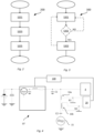
- Figure 1 schematically illustrates a cross sectional side view of an exemplifying embodiment of a plasma PVD apparatus 1 in accordance with the present disclosure.
- the apparatus may for example be used as an industrial deposition system.
- the apparatus 1 according to this exemplifying embodiment may be used for high-power impulse magnetron sputtering.
- the apparatus 1 comprises a process chamber 2 in the form of a vacuum chamber.
- the process chamber 2 may for example be essentially cylindrical, but is not limited thereto.
- At least one target 3 is arranged in the process chamber.
- the shape of the target may for example be planar rectangular, cylindrical, or hollow cylindrical, but is not limited thereto.
- the target 3 constitutes the cathode.
- the target 3 is mounted to a magnetron 4.
- the magnetron 4 may typically also provide the electrical connection of the target 3 to a power supply arrangement 10.
- the magnetron 4 may further comprise conduits for enabling cooling of the target (commonly water cooling).
- the magnetron 4 is arranged on the side of the target 3 which is opposite the side of the target 3 that faces the interior of the process chamber 2.
- the magnetron 4 generates a magnetic field (not shown) at the surface of the target 3 facing the interior of the process chamber 2. This magnetic field serves as a trap for electrons in the plasma.
- the apparatus 1 further comprises an anode, which may for example be in the form of an anode ring or any other previously known configuration therefore.
- anode which may for example be in the form of an anode ring or any other previously known configuration therefore.
- the walls of the process chamber may serve as the anode.
- the apparatus further comprises a power supply arrangement 10 configured to generate plasma discharges between the target and the anode.
- a plasma is generated in front of the surface of the target facing the interior of the process chamber 2.
- ions of a process gas such as argon
- the target has a lower potential than the region in which the plasma is formed and the target surface therefore attracts ions.
- the positive ions move towards the target with a high velocity and then impact the target, thereby causing atoms from the target to physically dislodge or sputter from the surface.
- the power supply arrangement 10 may be configured to operate in a pulsed power mode. Thereby, the power supply arrangement will generate plasma discharges during a number of consecutive pulses, each separated by a duration at which there is no active discharge. During the duration at which there is no active plasma discharge, the plasma will start to fade out until the following active discharge pulse.
- the apparatus 1 may further comprise a substrate holder 6 configured to hold one or more substrates 7 onto which for example a coating is to be deposited. In the figure, three different substrates 7 are shown.
- the substrate holder may be stationary or rotatably arranged during the deposition process. In case of the substrate holder being rotatably arranged, it may be configured for three-fold planetary rotation or simply rotatable around a single axis of rotation.
- the apparatus 1 may further comprise a bias supply device 8 connected to the substrate holder 6.
- the bias supply device 8 may be configured to supply a bias to each of the substrates 7 during the deposition process.
- the apparatus 1 further comprises a gas inlet 11.
- Process gas for example argon
- the apparatus may further comprise one or more additional gas inlets, if desired.
- the apparatus may comprise an auxiliary gas inlet intended for introduction of a reactive gas, if desired.
- the apparatus further comprises an exhaust 13 configured to allow gas to be led out of the process chamber 2.
- the apparatus 1 further comprises a radio frequency generator 15 configured to apply an oscillating voltage signal to the target 3. Thereby, the target may be provided with an oscillating potential.
- the radio frequency generator 15 is not intended to be used for the creation of plasma discharges and is therefore not to be confused with the power supply arrangement 10.
- the radio frequency generator 15 is intended simply for the purpose of enabling monitoring process conditions in the apparatus.
- the radio frequency generator may be configured to apply an oscillating voltage having a peak-to-peak amplitude of from 10 V to 300 V.
- the radio frequency generator may be configured to apply the oscillating voltage signal with a frequency of from 100 kHz to 1 MHz.
- the apparatus 1 further comprises a radio frequency sensor 16 configured to record a response from the oscillating voltage signal applied to the target 3 by means of the radio frequency generator 15.
- the apparatus 1 further comprises a control device 100 configured to control one or more of the constituent components of the apparatus 1. More specifically, the control device may be configured to control at least the radio frequency generator 15 and the radio frequency sensor 16. The control device may suitably also be configured to control the power supply arrangement 10. By way of example, the control device may be configured to control the pulse width, duty cycle, pulse frequency, and voltage as applied by the power supply arrangement to the target.
- the control device 100 may comprise one or more control units.
- each control unit may be configured to control a certain function or a certain function may be divided between more than one control units.
- the performance of the methods as described herein may be governed by programmed instructions.
- These programmed instructions typically take the form of a computer program P which, when executed in or by a control device (such as the control device 100), causes the control device to effect desired forms of action.
- Such instructions may typically be stored on a computer-readable medium.
- the apparatus 1 as described in the exemplifying embodiment shown in Figure 1 is intended for HiPIMS, the method for monitoring process conditions in a plasma PVD process is not limited to being performed in a HiPIMS process. It may be used in other plasma PVD processes, such as cathodic arc or pulsed DC magnetron sputtering.
- FIG 2 represents a flowchart schematically illustrating an exemplifying embodiment of a method 200 for monitoring process conditions in a plasma PVD process in accordance with the present disclosure.
- the plasma PVD process is performed in an apparatus as previously described, for example the apparatus 1 shown in Figure 1 .
- the method 200 comprises a step S201 of applying an oscillating voltage signal to the target by means of a radio frequency generator.
- the step S201 may be performed continuously, but the method is not limited thereto.
- the step S201 is performed at least when there is a desire to determine process conditions, i.e. when there is a plasma present in the process chamber. In other words, step S201 is performed when a plasma has been generated by means of the power supply arrangement.
- the method 200 further comprises a step S203 of recording a response from the applied oscillating voltage signal as applied by the radio frequency generator.
- the response is recorded by means of a radio frequency sensor.
- the method 200 further comprises a step S205 of deriving information regarding at least one plasma process condition at or in the close vicinity of the target. Said information is derived based on the response as recorded by the radio frequency sensor in step S203.
- FIG 3 represents a flowchart schematically illustrating an exemplifying embodiment of a method 300 for controlling a plasma PVD process in accordance with the present disclosure.
- the method 300 comprises a step S301 of performing the method 200 as described above with reference to Figure 2 .
- the method 300 may optionally further comprise a step S302 of determining whether or not there is a desire or need for adjusting input parameters to the power supply arrangement for the purpose of adjusting plasma process conditions in the apparatus.
- the step S302 would in such a case be performed based on the information derived in step S301.
- the step S302 may for example be performed by comparing the derived information regarding at least one plasma process condition with a corresponding reference range of said plasma process condition.
- the method may be reverted to step S301.
- the process further comprises a step S303 of, based on the derived information regarding at least one plasma process condition at or in the close vicinity of the target, adjusting an input signal to the power supply arrangement for the purpose of adjusting plasma process conditions in the apparatus if needed.
- the method 300 may suitably be repeated for the whole duration of the plasma PVD process. Thereby, relatively stable plasma process conditions may be obtained, which for example increases the quality of the resulting product of the process. Alternatively, the method 300 may for example be performed when there is an expected need for adjusting input parameters to the power supply arrangement.
- the method provides a procedure where simultaneously measured radio frequency current and voltage characteristics may be used to characterize the plasma.
- the first step is to carefully measure the applied RF voltage signal U s ( t ) and resulting RF current signal I s ( t ). This is carried out using an RF sensor, typically placed between the RF generator and the target.
- the resulting U s ( t ) and I s ( t ) waveforms may be recorded on an oscilloscope or a computer.
- the RF current signal can for example be measured by a current transformer and the voltage signal can for example be measured using a capacitive probe located inside the RF sensor. Details of such solutions are described by Sezemsky et al mentioned above.
- the RF sensor should preferably be calibrated in a wide frequency range, for example from 100 kHz to 3 MHz.
- the calibration can be performed using a frequency-independent resistance, resulting in voltage and current amplitude and phase correction factors.
- Correct measurements of the U s ( t ) and I s ( t ) waveforms may be obtained using discrete Fourier transformation (DFT) of the measured signals, where the DFT spectra are corrected with the amplitude and phase correction factors followed by inverse DFT transformation.
- DFT discrete Fourier transformation
- the above described calibrated measurements of U s ( t ) and I s ( t ) may be used to determine the relative phase ⁇ s ( t ) between U s ( t ) and I s ( t ). Using these values, the ion flux towards the target and the plasma sheath impedance at the target can be estimated as follows.
- the applied RF voltage signal to the target should have a sufficiently high amplitude (typically >10 V) to repel most of the electrons from the target surface. It is assumed that the electron contribution to the measured I s ( t ) in for example a typical HiPIMS process is close to zero when the amplitude of U s ( t ) is at least U s min ⁇ ⁇ 35 V . Therefore, a peak-to-peak amplitude of at least about 70 V could advantageously be used in case of a HiPIMS process.
- the total current measured at U s min is attributed only to positive ion current to the target.
- the plasma sheath impedance characterizes a measure of current flowing through the sheath, when there is a voltage across the sheath. Impedances measured in plasmas are commonly complex quantities because of the capacitive and inductive behavior of these discharges. Note that for a high-density plasma, which is the case in for example HiPIMS, the plasma impedance is negligible compared to the impedance of the sheath.
- U s pk t and I s pk t denote peak values of the measured RF probe voltage and current, respectively, and T is the period of the RF probe signal.
- the recorded signal is not given solely by the plasma sheath impedance Z pl ( t ), but also by the impedance of the target itself and the power feed line between the target and the RF sensor unit.
- This background impedance has a capacitive character, resulting in a displacement current added to the recorded RF current signal I s ( t ). Therefore, the background impedance should be measured using the same setup, but without a plasma, and subtracted from the calculated impedance Z s ( t ) in order to obtain the correct plasma sheath impedance.
- the same measurements of U s ( t ) and I s ( t ) can also be used to estimate the electron (plasma) density and electron temperature, again provided that the applied RF voltage signal to the target has a sufficiently high amplitude (typically >10 V).
- the method utilizes an approach described in detail by for example Müller et al, Towards Fast Measurement of the Electron Temperature in the SOL of ASDEX Upgrade Using Swept Langmuir Probes, Contrib. Plasma Phys. 50, 847 (2010 ), where highfrequency voltage sweeps were used during Langmuir probe diagnostics.
- the method is based on the transformation of data measured by the RF current/voltage sensor to Langmuir-like current-voltage characteristics, where each period of the RF voltage U s ( t ) is considered similar to a sweeping Langmuir probe voltage with a forward and a backward part.
- the above-described displacement current should be subtracted from the measured current signal I s ( t ) to get the total current I tot ( t ).
- the total current still contains a small capacitive current due to the differential sheath capacitance, which results in a difference in I tot ( t ) depending on the voltage sweep going in the forward or backward direction.
- the desired Langmuir-like current I p ( t ) is thereby obtained by substracting the capacitive current from the total current. Details of such solutions are described by Sezemsky et al. In this way, I p ( t ) can be plotted as a function of U s ( t ) and this characteristics can be further processed in a similar manner as Langmuir probe data. For example, the electron temperature T e (in units of eV) can be determined from the first derivative of the electron current in the I p ( t ) - U s ( t ) characteristics at the floating potential in a semi-logarithmic plot.
- Other quantities are as follows: q e the elementary charge, M i the ion mass, k B the Boltzmann constant, and T e the electron temperature in Kelvin.
- the ion flux to the target can be obtained by the radio frequency sensor recording the amplitude of the radio frequency voltage U s ( t ) and the current I s ( t ). Furthermore, by recording the complete waveforms of U s ( t ) and I s ( t ) it is possible to obtain information also regarding plasma sheath impedance, electron temperature and electron (plasma) density.
- the method utilizes the target as a probe instead of for example inserting a dedicated probe into the apparatus.
- Utilizing the target as the probe is not straight forward since the recorded response from the applied oscillating voltage, applied by means of the radio frequency generator, needs to be separated from power supplied by the power supply arrangement which is also connected to the target. This could for example be made by recording the response only when there is not active plasma discharge, for example by recording the response in the time between active discharge pulses or by a temporary short interruption of the plasma PVD process. It is however also possible to record the response during an active plasma discharge if the response can be adequately separated from the noise created by the power supply arrangement.
- the radio frequency generator must also be protected from the power supplied by the power supply arrangement, and it should be ensured that the power supplied by the power supply arrangement is utilized for creating the intended plasma discharge(s) instead of being lost in the radio frequency generator.
- Figure 4 schematically illustrates one example of how the power supply arrangement, the radio frequency generator and the radio frequency sensor may be connected in a HiPIMS apparatus.
- a HiPIMS power supply arrangement 10' is connected to the magnetron 4.
- the cable connecting the HiPIMS power supply arrangement with the magnetron has a parasitic capacitance C1.
- the radio frequency generator 15 is connected to the magnetron 4 via a capacitor C2 in order to protect the radio frequency generator 15 from the HiPIMS power supply.
- the radio frequency sensor 16 (see Figure 1 ) comprises a radio frequency voltage probe 16a and a current probe 16b. These probes 16a and 16b of the radio frequency sensor 16 detect the radio frequency voltage and current signals, respectively.
- Probe 16a comprises a first sensing resistor R1 which may be used when measuring the target voltage.
- Probe 16b comprises a second sensing resistor R2 over which the induced target current can be measured as a voltage drop.
- Signals from probes 16a and 16b of the radio frequency sensor 16 are led to for example a digital oscilloscope 20 for further processing of the data.
- the digital oscilloscope 20 may be connected to a control device 100.
- the control device 100 may further be connected to the HiPIMS power supply arrangement 10'.
- the HiPIMS power supply used in the experiments, had a configuration as described in M. ⁇ ada, Z. Hubi ⁇ ka, P. Adámek, J. Kluso ⁇ , and L Jastrabik, Surf. Coatings Technol. 205, S317 (2011).
- a time-averaged discharge power of 250 W was kept constant in all experiments by varying the discharge voltage.
- the pulse on-time and pulse frequency were fixed at 100 ⁇ s and 100 Hz, respectively.
- the experimental setup for measuring the plasma sheath impedance at the target, the ion flux towards the target as well as the electron (plasma) density and electron temperature at the target was as described above with reference to Figure 4 .
- the target RF voltage was provided by a Tabor Electronics 9100 high-voltage wideband amplifier with a fixed gain connected to a function generator, Agilent 33220A.
- the function generator was set to deliver a sinusoidal 350 kHz signal. After amplification the signal had a peak-to-peak value of U s pk ⁇ 70 V on the target.
- the target voltage and current were monitored on an Agilent InfiniiVision DSO7104B oscilloscope.
- FIGS 5a and 5b An example of the target voltage and current characteristics when superimposing the RF voltage signal in a HiPIMS process are shown in Figures 5a and 5b , respectively.
- the RF voltage signal was continuously applied during the whole time, which means that it is present both during the HiPIMS discharge pulse as well as between consecutive discharge pulses without any interruption.
- the iron target was sputtered in pure argon working gas at a flow rate of 26 sccm using the experimental setup described above, without any introduction of oxygen gas.
- the iron target was sputtered in a working gas mixture of argon (flow rate 26 sccm) and oxygen (flow rate 2 sccm) using the experimental setup described above.
- Measured electron temperatures are in the range of a few eV, which is well in agreement with probe measurements by Sezemsky et al., Modified high frequency probe approach for diagnostics of highly reactive plasma, Plasma Sources Sci. Technol. 28, 115009 (2019 ), who used the same analysis method as described in the theoretical considerations.
- Figure 6a illustrates the target voltage over time
- Figure 6b illustrates the target current over time
- Figure 6c illustrates the target power over time.
- the applied oscillating voltage becomes evident a few microseconds after the HiPIMS pulse has ended.
- the power at the target firstly increases as a result of the increased amplitude of the oscillating voltage.
- the power shown in Figure 6c may be compared with the time-averaged discharge power of 250 W of the HiPIMS power supply arrangement.
Landscapes
- Chemical & Material Sciences (AREA)
- Engineering & Computer Science (AREA)
- Organic Chemistry (AREA)
- Materials Engineering (AREA)
- Mechanical Engineering (AREA)
- Metallurgy (AREA)
- Chemical Kinetics & Catalysis (AREA)
- Physics & Mathematics (AREA)
- Plasma & Fusion (AREA)
- Spectroscopy & Molecular Physics (AREA)
- Electromagnetism (AREA)
- Analytical Chemistry (AREA)
- Plasma Technology (AREA)
- Physical Vapour Deposition (AREA)
- Other Resins Obtained By Reactions Not Involving Carbon-To-Carbon Unsaturated Bonds (AREA)
Description
- The present disclosure relates in general to a method for monitoring process conditions in a plasma PVD process. The present disclosure further relates in general to a method for controlling a plasma PVD process. The present disclosure further relates in general to a computer program and a computer-readable medium. The present disclosure also relates in general to a plasma PVD process apparatus.
- Physical vapor deposition (PVD) is a generic term for a variety of different processes which may be used for production of thin films, coatings or nanoparticles. According to these processes, a source material goes from a solid phase (or in some rare cases, a liquid state) to a vapor phase and then again to a solid state, for example as a thin film on a substrate. The most common PVD processes include sputtering, wherein atoms or particles are physically ejected from the source material, and evaporation, wherein the source material is evaporated to the vapor phase.
- With the introduction of various ionized physical vapor deposition (IPVD) processes, the possibility to ionize and accelerate a substantial fraction of the deposition flux has opened up new ways to tailor thin films with improved properties. One example of an IPVD method currently gaining a lot of interest is high-power impulse magnetron sputtering (HiPIMS). HiPIMS utilizes very high power densities of the order of kW/cm2, averaged over the active cathode surface, in short pulses at a low duty cycle, usually <10 %. By means of HiPIMS, it is inter alia possible to obtain a very high degree of ionization of the sputtered source material.
- Many PVD processes suffer from the problem of the process parameters not being stable, both in the short-time frame (seconds) and in the long-time frame (minutes and hours). For the purpose of providing a more stable process, it would be desirous to be able to continuously, or regularly, determine the process parameters and based on the data, shift and guide the input parameters of the PVD process. However, commonly known measurement methods for determining certain process parameters defining plasma characteristics are complex and some are even likely to disturb the process. The latter can in turn be very costly in a production environment, for example if resulting in a whole batch having an inferior quality of the resulting film or nanoparticles.
- A previously known technique to analyze sputtering plasma conditions is to utilize a probe connected to a radio frequency bias voltage source and perform precise probe RF voltage and RF current waveform measurements. A proper analysis of the measured signals allows determining ion flux to the probe surface. The method was originally proposed by Sobolewski in the 1990s (see M.A. Sobolewski, J. Vac. Sci. Technol. A 10, 3550 (1992)).
- D. Lundin et al., Time-resolved ion flux and impedance measurements for process characterization in reactive high-power impulse magnetron sputtering, Journal of Vacuum Science & Technology A34, 041305 (2016), discloses a planar ion flux probe, based on the so called Sobolewski method for time-resolved plasma characterization. The probe was evaluated in a high-power impulse magnetron sputtering (HiPIMS) process. The probe was placed at the substrate position and time-resolved measurements of the absolute ion flux impinging on the probe, as well as the probe sheath impedance, were recorded during the HiPIMS pulse.
-
US 2009/045046 A1 discloses a method of responding to voltage or current transients during processing of a wafer in a plasma reactor at each of a plurality of RF power applicators and at the wafer support surface. -
US 2002/124959 A1 discloses a plasma monitoring method and a semiconductor production device, which may be a sputtering apparatus. In the sputtering apparatus, a target is placed on an electrode which is electrically connected to an RF probe, and a radio-frequency wave generator. Ar gas is discharged by a radio-frequency wave, generated by the radio-frequency generator, into a plasma state. The voltage and current of the radio-frequency wave are measured with the RF probe, and a judgement device judges the state of the plasma. - The object of the present invention is to further improve the ability to determine process conditions in a plasma PVD process while at the same time seek to avoid the risk of disturbing the plasma PVD process.
- The object is achieved by means of the subject-matter of the appended independent claims.
- In accordance with the present disclosure, a method for monitoring process conditions in a plasma PVD, performed in an apparatus, is provided. The apparatus comprises a process chamber, a target arranged inside the process chamber, and a power supply arrangement connected to the target and configured to generate plasma discharges. The apparatus further comprises a radio frequency generator and a radio frequency sensor. The method comprises a step of, when a plasma has been generated by means of the power supply arrangement, applying an oscillating voltage signal to the target by means of the radio frequency generator. The method further comprises a step of recording a response from the applied oscillating voltage signal by means of the radio frequency sensor. The method further comprises a step of, based on the recorded response, deriving information regarding at least one plasma process condition at or in the close vicinity of the target.
- By means of the present method, the target will in addition to acting as a plasma generating electrode also act as a probe used for determining plasma process conditions. Thereby, no additional hardware needs to be inserted into the process chamber. Thereby, the present method may be performed essentially without disturbing the plasma PVD process, which in turn minimizes the risk of loss of production speed or reduced quality of the produced thin film or nanoparticles.
- Furthermore, by means of the present method, reliable information regarding the plasma characteristics at the target can be obtained. This inter alia enables an improved possibility for active control of the plasma PVD process in situ, which in turn enables obtaining a more stable plasma PVD process. Moreover, the information regarding the plasma characteristics improves the traceability of the process conditions.
- The step of recording a response from the applied oscillating voltage signal comprises recording the response current amplitude and current phase shift. By knowing the current amplitude and the current phase shift, it is possible to obtain information regarding ion flux to the target surface as well as plasma sheath impedance at the target. Furthermore, information regarding the electron density and the electron temperature at the target can be derived.
- The oscillating voltage signal is applied with a frequency of from 100 kHz to 1 MHz. Thereby, it is ensured that the frequency is much lower than the ion plasma frequency. At the same time, such a frequency enables a very good time resolution.
- The peak-to-peak amplitude of the applied oscillating voltage signal may suitably be from 10 V to 300 V. Thereby, the amplitude is sufficiently high for the electron contribution to the recorded response to be negligible, but at the same time sufficiently low so as to not cause alterations to the plasma PVD process.
- The power supply arrangement may be configured to operate in a pulsed mode. In such a case, the step of deriving information regarding at least one plasma process condition may suitably be performed based on a response recorded in between two active plasma discharge pulses as applied by the power supply arrangement. Thereby, it can be avoided having to isolate the recorded response from the power supplied by the power supply arrangement during an active discharge. This in turn significantly facilitates the method. Although there is no active plasma discharge pulse when the response is recorded, there will still be a remnant plasma in the apparatus. Since the present method has a very good time resolution, the time delay from the active plasma discharge to the time at which the response is recorded may be sufficiently short for the fading out of the plasma to be negligible.
- According to one aspect, the plasma PVD process may be high-power impulse magnetron sputtering.
- Moreover, the method may further comprise, during operation of the plasma PVD process, applying a second oscillating voltage signal to a probe arranged at a substrate position, recording the response from the second applied oscillating voltage signal. The method may further comprise, based on the recorded response from the second applied oscillating voltage, deriving information regarding at least one plasma process condition at the substrate position. Thereby, further information regarding the processing conditions during the plasma PVD process can be obtained, more specifically at the substrate position. This in turn further improves the traceability of the process conditions as well as further enables improved active control of the plasma PVD process in situ for the purpose of obtaining a more stable process and/or to achieve desired thin film or nanoparticle properties.
- The present disclosure further provides a method for controlling a plasma PVD process, for example a high-power impulse magnetron sputtering process, performed in an apparatus. The apparatus comprises a process chamber, a target arranged inside the process chamber, and a power supply arrangement connected to the target and configured to generate plasma discharges. The apparatus further comprises a radio frequency generator and a radio frequency sensor. The method for controlling a plasma PVD process comprises a step of performing the method for monitoring process conditions in a plasma PVD process as described above, thereby deriving information regarding at least one plasma process condition. The method for controlling a plasma PVD process further comprises a step of, based on the derived information regarding at least one plasma process condition at or in the close vicinity of the target, adjusting an input signal to the power supply arrangement for the purpose of adjusting plasma process conditions in the apparatus. Alternatively, or additionally, the method for controlling a plasma PVD process comprises a step of, based on the derived information regarding at least one plasma process condition at or in the close vicinity of the target, adjusting an input signal to a gas supply device configured to introduce process gas into the process chamber, for the purpose of adjusting plasma process conditions in the apparatus.
- The method for controlling the plasma PVD process may be performed continuously during the plasma PVD process. Thereby, a more stable plasma PVD process may be achieved.
- The present disclosure further relates to a computer program, wherein said computer program comprises instructions for causing a control device to perform any one of the methods described above.
- The present disclosure further relates to a computer-readable medium comprising instructions, which when executed by a control device, cause the control device to perform any one of the methods as described above.
- Moreover, in accordance with the present disclosure, a plasma PVD process apparatus is provided. The plasma PVD process apparatus comprises:
- a process chamber configured to comprise a target;
- a power supply arrangement configured to be connected to the target and configured to provide plasma discharges;
- a radio frequency generator configured to apply an oscillating voltage signal, with a frequency of from 100 kHz to 1 MHz, to the target when a plasma has been generated by means of the power supply arrangement;
- a radio frequency sensor configured to record a response from the applied oscillating voltage signal to the target; and
- a control device configured to derive information regarding at least one plasma process condition at, or in the close vicinity of, the target based on the response recorded by the radio frequency sensor, wherein the recorded response comprises a response current amplitude and current phase shift.
- The plasma PVD apparatus has the advantages described above with reference to the corresponding methods.
- The power supply arrangement may be configured to be operated in a pulsed mode. In such a case, the control device may be configured to derive information regarding the at least one plasma process condition based on the response recorded by the radio frequency sensor between plasma discharge pulses applied by the power supply arrangement.
- The control device may further be configured to adjust an input signal to the power supply arrangement, and/or an input signal to a gas supply device configured to introduce process gas into the process chamber, based on the derived information regarding at least one plasma process condition at or in the close vicinity of the target. The purpose of such an adjustment is to adjust the process conditions in situ.
- The plasma PVD process apparatus may for example be a high-power impulse magnetron sputtering apparatus.
-
- Fig. 1
- schematically illustrates a cross sectional view of one exemplifying embodiment of a plasma PVD apparatus in accordance with the present disclosure;
- Fig. 2
- represents a flowchart schematically illustrating one exemplifying embodiment of a method for monitoring process conditions in a plasma PVD process according to the present disclosure;
- Fig. 3
- represents a flowchart schematically illustrating one exemplifying embodiment of a method for control of a plasma PVD process in accordance with the present disclosure;
- Fig. 4
- schematically illustrates one example of a possible connection between a HiPIMS power supply arrangement, a magnetron, a radio frequency generator and a radio frequency sensor;
- Fig. 5a
- shows an example of target voltage characteristics when an oscillating voltage signal is superimposed by means of a radio frequency generator in a HiPIMS process;
- Fig. 5b
- shows the corresponding target current characteristics when superimposing an oscillating voltage signal in the HiPIMS process as shown in
Figure 5a ; - Fig. 6a
- shows an example of target voltage over time, after an HiPIMS pulse, when an oscillating voltage signal is applied to a target;
- Fig. 6b
- shows an example of target current over time, after an HiPIMS pulse, when an oscillating voltage signal is applied to a target; and
- Fig. 6c
- shows an example of target power over time, after an HiPIMS pulse, when an oscillating voltage signal is applied to a target.
- The present invention will in the following be described in more detail with reference to various exemplifying embodiments and the drawings, as well as experimental results. The invention is however not limited to the exemplifying embodiments or experimental results described but may be varied within the scope of the independent claim(s). Furthermore, the drawings shall not be considered drawn to scale as some feature may be exaggerated in order to more clearly illustrate features therein.
- In the present disclosure, the term "target" should be interpreted broadly and thus encompasses any plasma generating electrode in a physical vapor deposition process. In a deposition process, the target may be formed of the source material which is to be sputtered (or possibly evaporated) from the surface of the target.
- In accordance with the present disclosure, a method for monitoring process conditions in a plasma physical vapor deposition (PVD) process is provided. The method provides real-time process characterization in for example deposition systems used for volume production, without the need to introduce any additional equipment inside the process chamber. Thus, the method according to the present disclosure avoids the need of introducing a separate probe into the process chamber, although this may also be performed to derive further information if desired.
- Furthermore, by means of the present method, information regarding the process conditions at the target surface or in the close vicinity thereof may be obtained in real time. This information is highly relevant since it inter alia governs the ionization degree of the sputtered material from the target, which in turn governs the possible degree of ionization of the material flux arriving at the substrate and thus enables tailoring of film texture and microstructure. The method can also provide information on the chemical state of the source material, which enables process stabilization and higher deposition rates when using reactive working gases. Process conditions in the volume close to the target surface may otherwise be very difficult to reliably measure in real time, especially in industrial deposition systems.
- The method for monitoring process conditions in a plasma PVD process according to the present disclosure further has the advantage of being able to use in comparatively dirty industrial plasma PVD processes since the data acquisition is not adversely affected by erosion or contamination of the target used to collect the required information. For essentially the same reason, the present method may be used in reactive processes in which a reactive gas is introduced during the process for the purpose of for example producing compound coatings on a substrate.
- The method for monitoring process conditions in a plasma PVD process according to the present disclosure is performed in an apparatus comprising a process chamber (such as a vacuum chamber), a target arranged inside the process chamber, a power supply arrangement connected to the target and configured to generate plasma discharges inside the process chamber. The apparatus may be any previously known apparatus for performing the plasma PVD process and typically comprises at least a process chamber and a power supply arrangement configured to generate plasma discharges inside the process chamber. The power supply arrangement may for example be a HiPIMS power supply arrangement, a RF power supply arrangement, a (pulsed or un-pulsed) DC power supply arrangement, or a microwave power supply arrangement. During the plasma PVD process, a target is arranged inside the apparatus. In contrast to such previously known apparatuses, the apparatus wherein the present method is performed is supplemented with a radio frequency generator and a radio frequency sensor. The radio frequency generator is a separate device from the power supply arrangement. In other words, said radio frequency generator is not used for generating, or sustaining, a plasma. Instead, the radio frequency generator is configured to apply an (auxiliary) oscillating voltage signal to the target which is separate from the power supplied by the power supply arrangement for the purpose of generating and/or sustaining a plasma discharge. The radio frequency sensor may suitably be connected to the radio frequency generator so as to also being able to record the applied oscillating voltage signal in addition to the response from the applied oscillating voltage. The method for monitoring process conditions in a plasma PVD process is performed by a control device configured therefore.
- The method comprises a step of, when a plasma has been generated by means of the power supply arrangement, applying an oscillating voltage signal to the target by means of the radio frequency generator. The oscillating voltage signal may for example be applied continuously to the target during the operation of the plasma PVD process, or at preselected time intervals. The oscillating voltage may for example be applied with a frequency of between 100 kHz and 1 MHz (including the end values of the range), preferably from 250 kHz to 500 kHz. Such a frequency will give a time resolution in the order of a few microseconds and will therefore for example enable obtaining relevant information regarding the plasma process conditions even when there is no active plasma discharge applied by the power supply arrangement (but a remnant plasma from a previous plasma discharge). The peak-to-peak amplitude of the applied oscillating voltage may suitably be between 10 V and 300 V (including the end values), preferably from 40 V to 100 V. Thereby, it is inter alia ensured that the applied oscillating voltage is sufficiently high for the electron contribution to the recorded response to be negligible. Furthermore, it is ensured that the applied oscillating voltage is sufficiently low so as to not cause substantial negative effects to the plasma PVD process as such. The applied oscillating voltage signal may be a sinusoidal shaped voltage signal. Moreover, the oscillating voltage potential applied by the radio frequency generator is not sufficient to generate or sustain a plasma discharge. The maximum power generated by the application of the oscillating voltage signal to the target by means of the radio frequency generator may typically be less than 10%, or even less than 5%, of the time-averaged power supplied to the target by means of the power supply arrangement. According to an example, the maximum power generated by the application of the oscillating voltage signal to the target by means of the radio frequency generator may be equal to or less than 2%, of the time-averaged power supplied to the target by means of the power supply arrangement.
- The method further comprises a step of recording the response from the applied oscillating voltage signal by means of the radio frequency sensor. More specifically, the method comprises a step of recording the response of the plasma from the applied oscillating voltage signal. The radio frequency sensor is for said purpose connected to the target. The step of recording a response of the plasma from the applied oscillating voltage signal may comprise recording the response current amplitude. By knowing the response current amplitude and the amplitude of the applied oscillating voltage, it is possible to derive information regarding ion flux to the target surface. The step of recording a response from the applied oscillating voltage signal may also comprise recording the current phase shift, i.e. the relative phase between the oscillating voltage signal and the current response. More specifically, the step of recording a response from the applied oscillating voltage signal may comprise recording the current and voltage waveforms, as well as the current and voltage amplitudes. For the purpose of knowing the amplitude and/or the waveform of the oscillating voltage signal as applied by the radio frequency generator, the radio frequency sensor may preferably be configured to record said applied oscillating voltage signal. This in turn increases the reliability since it can be ensured that the time at which the applied oscillating voltage is accurate in relation to the recorded response, and there is essentially no risk for errors which may occur if relying on input parameters to the radio frequency generator. It should however be noted that measurements of radio frequency signals should be adequately calibrated. The skilled person is however aware of techniques therefore and this will therefore not be described in detail here.
- The method further comprises a step of, based on the recorded response, deriving information regarding at least one plasma process condition at or in the close vicinity of the target. The information may for example be derived by calculation of the plasma process condition from the recorded response. In such a calculation, the displacement currents may be subtracted from the recorded response.
- Examples of plasma process conditions which may be derived by means of the method for monitoring process conditions in accordance with the present disclosure includes the ion flux to the target surface, the plasma sheath impedance at the target, the electron temperature in the close vicinity of the target as well as electron density in the vicinity of the target. From these process conditions, further information may be obtained. For example, the chemical state of the source material (i.e. the target material) can be obtained by determining the plasma sheath impedance at the target. Furthermore, the ion fraction of the sputtered material can be obtained from the electron density and electron temperature at the target.
- By means of the present method, the target will in practice function as a probe in addition to its function as a plasma generating electrode.
- The method described above may be performed continuously during the plasma PVD process, or at preselected time intervals as desired. Furthermore, the method described above may also be performed during a temporary interruption of the plasma PVD process. Such a temporary interruption may be performed for the sole basis of enabling performing the method for monitoring according to the present disclosure. Performing the method during a temporary interruption is useful for example in case of plasma PVD processes where the plasma discharges are not provided in a pulsed mode. For other situations, it is generally more relevant to perform the method continuously or at preselected time intervals. In case of performing the method during a temporary interruption, the step of recording a response from the applied oscillating voltage signal should be performed as soon as possible after the interruption of the plasma PVD process in order for the plasma to still be present and for obtaining the most relevant information. This would preferably be in the order of a few microseconds after interruption of the plasma discharge.
- The information derived regarding process conditions, resulting from the above described method for monitoring process conditions can be further utilized for various purposes. For example, the derived data may be used for the purpose of traceability of obtained plasma conditions. Moreover, the derived data may be used for the purpose of improving the repeatability of intended process conditions. This can be done by using the derived information for the purpose of controlling the plasma PVD process as will be further described below. Furthermore, the derived data allows for a wider process parameter space available for the development and production of thin films and coatings for different applications. This is due to enabling more stable process conditions for the PVD process by improving the ability to active control the plasma PVD process in situ. Furthermore, the method may advantageously be used also in reactive deposition systems since the ability to in situ monitor the process conditions may improve the active control of the reactive PVD process when operating under unstable conditions. This may in turn improve the quality of the deposited compound film.
- The method for monitoring process conditions in a plasma PVD process may in practice be performed in any plasma PVD process as long as the response from the applied oscillating voltage can be identified and isolated from the noise. Here it should be recognized that the oscillating voltage potential applied by the radio frequency generator is of a considerably lower power than the power applied to create plasma discharges. Examples of plasma PVD processes wherein the present method may be utilized include for example DC magnetron sputtering and cathodic arc deposition (which is an evaporation process), but are not limited thereto. The method is however greatly facilitated in case of being performed in pulsed plasma PVD processes, wherein the plasma discharges are provided in pulses. This is due to the ability to record the response from the applied oscillating voltage signal at a time between active plasma discharge pulses. Thereby, the response need not be isolated from the "noise" formed by the applied power used to obtain the plasma discharge (i.e. the power provided by the power supply arrangement). By recording the response from the applied oscillating voltage shortly after termination of an active plasma discharge pulse, there will still be a remaining plasma in the process chamber. In case of recording the response essentially immediately after termination of an active plasma discharge pulse, the plasma may still be existing to some degree (sometimes referred to as an "afterglow plasma").
- Therefore, the method for monitoring process conditions in a plasma PVD process may suitably be performed in a pulsed plasma PVD process. This means that the power supply arrangement is configured to operate in a pulsed mode.
- One example of such a process is the high-power impulse magnetron sputtering (HiPIMS) process. HiPIMS is based on magnetron sputtering, but utilizes very high power densities applied to the target in short pulses (impulses). The peak power density could typically be in the order of kW/cm2 or even MW/cm2 over the target surface. The peak discharge current density can reach several A/cm2 over the target surface. In order to avoid overheating or other damages of the target, the pulses are applied with a low duty cycle, typically <10%. Despite the low duty cycle, the average discharge power over time can be at least essentially the same as the time-averaged discharge power in conventional magnetron sputtering. HiPIMS inter alia has the advantage of enabling a very high degree of ionization of the sputtered material. The HiPIMS process can also be conducted as a bipolar HiPIMS process, wherein the active discharge pulses are each followed by a pulse with reversed polarity to the target. When performing the method for monitoring process conditions in accordance with the present disclosure in a HiPIMS process, the step of recording the response from the applied oscillating voltage signal can easily be performed during the period between active discharge pulses.
- Other examples of pulsed plasma PVD processes wherein the method for monitoring plasma process conditions according to the present disclosure may be easily used include pulsed cathodic arc deposition or pulsed DC magnetron sputtering, in particular asymmetric bipolar DC magnetron sputtering.
- In a cathodic arc deposition process, an electric arc is used to vaporize material from a target. In this process, a high current, low voltage arc is used to strike the surface of the target in a so-called cathode spot. The localized temperature in the cathode spot is extremely high, which results in a high velocity jet of vaporized material from the target. The cathode spot is only active for a short period of time. The arc can be influenced by application of an electromagnetic field for the purpose of rapidly moving the arc over the surface of the target. In a pulsed cathodic arc process, the arc is provided in a pulsed mode which means that there are times during the process at which there is no active discharge arc. During said periods, the step of recording the response from the applied oscillating voltage can easily be achieved.
- In pulsed DC magnetron sputtering, a pulsed DC electrical current (typically of a few hundreds of volts) is applied to the target. A pulsed magnetron sputtering arrangement can be either asymmetric bipolar pulsed or unipolar pulsed. Asymmetric bipolar pulsed is frequently used for deposition of insulating films from conductive targets through reactive sputtering, since it can still operate in conditions where the target is partially covered by insulating material. In pulsed DC operation, pulsing of the magnetron sputtering discharge is often in the frequency range of 10-250 kHz and the duty cycle is typically 50-90%.
- The above described method for monitoring process conditions in a plasma PVD process may further be supplemented by an oscillating voltage signal to a probe at a substrate position in the apparatus, recording the response from said applied oscillating voltage signal, and, based on the responded response, deriving information regarding at least one plasma process condition at the substrate position. This may for example be made by applying the oscillating voltage signal to the substrate itself. Thereby, it is possible to also obtain knowledge regarding the conditions at the substrate position. Thereby, plasma process conditions may be determined at the most relevant volumes of the process chamber.
- The above described method for monitoring process conditions in a plasma PVD process may naturally be further supplemented, if desired, with further techniques for determining process conditions. By way of example, a separate probe may be introduced into the apparatus at another location than described above. An oscillating voltage may be applied to said separate probe and the response recorded. Furthermore, other techniques such as a Langmuir probe, OES analysis or the like may be utilized as previously known in the art, if desired.
- The present disclosure further relates to a method for controlling a plasma PVD process. The method for controlling a plasma PVD process comprises a step of performing the method for monitoring process conditions as described above, thereby deriving information regarding at least one plasma process condition. The method for controlling a plasma PVD process further comprises a step of, based on the derived information regarding at least one plasma process condition at or close to the target, adjusting an input signal to the power supply arrangement for the purpose of adjusting plasma process conditions in the apparatus. Alternatively, or additionally, the method for controlling a plasma PVD process comprises a step of, based on the derived information regarding at least one plasma process condition at or close to the target, adjusting an input signal to a gas supply device configured to introduce process gas into the process chamber and/or an input signal to a magnetic field generating device to adjust the magnetic field arrangement (in case of a tunable magnetic field) of the apparatus.
- The method for controlling the plasma PVD process may suitably be performed continuously during the plasma PVD process. This also implies that the step of performing the method for monitoring plasma process conditions, as such, is performed continuously during the plasma PVD process. The term "continuously" is in this context considered to mean that it is performed repeatedly without interruption during the plasma PVD process.
-
Figure 1 schematically illustrates a cross sectional side view of an exemplifying embodiment of aplasma PVD apparatus 1 in accordance with the present disclosure. The apparatus may for example be used as an industrial deposition system. Theapparatus 1 according to this exemplifying embodiment may be used for high-power impulse magnetron sputtering. - The
apparatus 1 comprises aprocess chamber 2 in the form of a vacuum chamber. Theprocess chamber 2 may for example be essentially cylindrical, but is not limited thereto. At least onetarget 3 is arranged in the process chamber. The shape of the target may for example be planar rectangular, cylindrical, or hollow cylindrical, but is not limited thereto. During sputtering of the material from the target, thetarget 3 constitutes the cathode. Thetarget 3 is mounted to amagnetron 4. Themagnetron 4 may typically also provide the electrical connection of thetarget 3 to apower supply arrangement 10. Themagnetron 4 may further comprise conduits for enabling cooling of the target (commonly water cooling). Themagnetron 4 is arranged on the side of thetarget 3 which is opposite the side of thetarget 3 that faces the interior of theprocess chamber 2. Themagnetron 4 generates a magnetic field (not shown) at the surface of thetarget 3 facing the interior of theprocess chamber 2. This magnetic field serves as a trap for electrons in the plasma. - The
apparatus 1 further comprises an anode, which may for example be in the form of an anode ring or any other previously known configuration therefore. Alternatively, the walls of the process chamber may serve as the anode. - The apparatus further comprises a
power supply arrangement 10 configured to generate plasma discharges between the target and the anode. Thereby, a plasma is generated in front of the surface of the target facing the interior of theprocess chamber 2. During a deposition process, ions of a process gas (such as argon) are generated in the plasma and drawn out of the plasma and accelerated across a cathode sheath. The target has a lower potential than the region in which the plasma is formed and the target surface therefore attracts ions. The positive ions move towards the target with a high velocity and then impact the target, thereby causing atoms from the target to physically dislodge or sputter from the surface. - The
power supply arrangement 10 may be configured to operate in a pulsed power mode. Thereby, the power supply arrangement will generate plasma discharges during a number of consecutive pulses, each separated by a duration at which there is no active discharge. During the duration at which there is no active plasma discharge, the plasma will start to fade out until the following active discharge pulse. - The
apparatus 1 may further comprise asubstrate holder 6 configured to hold one ormore substrates 7 onto which for example a coating is to be deposited. In the figure, threedifferent substrates 7 are shown. The substrate holder may be stationary or rotatably arranged during the deposition process. In case of the substrate holder being rotatably arranged, it may be configured for three-fold planetary rotation or simply rotatable around a single axis of rotation. Theapparatus 1 may further comprise abias supply device 8 connected to thesubstrate holder 6. Thebias supply device 8 may be configured to supply a bias to each of thesubstrates 7 during the deposition process. - The
apparatus 1 further comprises agas inlet 11. Process gas, for example argon, may be introduced via thegas inlet 11 by means of agas supply device 12 of the apparatus. The apparatus may further comprise one or more additional gas inlets, if desired. For example, the apparatus may comprise an auxiliary gas inlet intended for introduction of a reactive gas, if desired. The apparatus further comprises anexhaust 13 configured to allow gas to be led out of theprocess chamber 2. - The
apparatus 1 further comprises aradio frequency generator 15 configured to apply an oscillating voltage signal to thetarget 3. Thereby, the target may be provided with an oscillating potential. Theradio frequency generator 15 is not intended to be used for the creation of plasma discharges and is therefore not to be confused with thepower supply arrangement 10. Theradio frequency generator 15 is intended simply for the purpose of enabling monitoring process conditions in the apparatus. - The radio frequency generator may be configured to apply an oscillating voltage having a peak-to-peak amplitude of from 10 V to 300 V. The radio frequency generator may be configured to apply the oscillating voltage signal with a frequency of from 100 kHz to 1 MHz. The
apparatus 1 further comprises aradio frequency sensor 16 configured to record a response from the oscillating voltage signal applied to thetarget 3 by means of theradio frequency generator 15. - The
apparatus 1 further comprises acontrol device 100 configured to control one or more of the constituent components of theapparatus 1. More specifically, the control device may be configured to control at least theradio frequency generator 15 and theradio frequency sensor 16. The control device may suitably also be configured to control thepower supply arrangement 10. By way of example, the control device may be configured to control the pulse width, duty cycle, pulse frequency, and voltage as applied by the power supply arrangement to the target. - The
control device 100 may comprise one or more control units. In case of the control device comprising a plurality of control units, each control unit may be configured to control a certain function or a certain function may be divided between more than one control units. - The performance of the methods as described herein may be governed by programmed instructions. These programmed instructions typically take the form of a computer program P which, when executed in or by a control device (such as the control device 100), causes the control device to effect desired forms of action. Such instructions may typically be stored on a computer-readable medium.
- It should be noted that although, the
apparatus 1 as described in the exemplifying embodiment shown inFigure 1 is intended for HiPIMS, the method for monitoring process conditions in a plasma PVD process is not limited to being performed in a HiPIMS process. It may be used in other plasma PVD processes, such as cathodic arc or pulsed DC magnetron sputtering. -
Figure 2 represents a flowchart schematically illustrating an exemplifying embodiment of amethod 200 for monitoring process conditions in a plasma PVD process in accordance with the present disclosure. The plasma PVD process is performed in an apparatus as previously described, for example theapparatus 1 shown inFigure 1 . Themethod 200 comprises a step S201 of applying an oscillating voltage signal to the target by means of a radio frequency generator. The step S201 may be performed continuously, but the method is not limited thereto. The step S201 is performed at least when there is a desire to determine process conditions, i.e. when there is a plasma present in the process chamber. In other words, step S201 is performed when a plasma has been generated by means of the power supply arrangement. - The
method 200 further comprises a step S203 of recording a response from the applied oscillating voltage signal as applied by the radio frequency generator. The response is recorded by means of a radio frequency sensor. - The
method 200 further comprises a step S205 of deriving information regarding at least one plasma process condition at or in the close vicinity of the target. Said information is derived based on the response as recorded by the radio frequency sensor in step S203. -
Figure 3 represents a flowchart schematically illustrating an exemplifying embodiment of amethod 300 for controlling a plasma PVD process in accordance with the present disclosure. Themethod 300 comprises a step S301 of performing themethod 200 as described above with reference toFigure 2 . Themethod 300 may optionally further comprise a step S302 of determining whether or not there is a desire or need for adjusting input parameters to the power supply arrangement for the purpose of adjusting plasma process conditions in the apparatus. The step S302 would in such a case be performed based on the information derived in step S301. The step S302 may for example be performed by comparing the derived information regarding at least one plasma process condition with a corresponding reference range of said plasma process condition. If there is no need to adjust the input parameters to the power supply apparatus, the method may be reverted to step S301. The process further comprises a step S303 of, based on the derived information regarding at least one plasma process condition at or in the close vicinity of the target, adjusting an input signal to the power supply arrangement for the purpose of adjusting plasma process conditions in the apparatus if needed. - The
method 300 may suitably be repeated for the whole duration of the plasma PVD process. Thereby, relatively stable plasma process conditions may be obtained, which for example increases the quality of the resulting product of the process. Alternatively, themethod 300 may for example be performed when there is an expected need for adjusting input parameters to the power supply arrangement. - In the following, theoretical considerations for deriving information regarding at least one plasma process condition at or in the close vicinity of the target will be described. These theoretical considerations are similar to those described for example in Sezemsky et al., Modified high frequency probe approach for diagnostics of highly reactive plasma, Plasma Sources Sci. Technol. 28, 115009 (2019), but with the important difference of the target functioning as the probe instead of a separate probe inserted into the plasma.
- By means of the applying an oscillating voltage signal to the target using a radio frequency generator and recording the response from the applied oscillating voltage signal, various plasma process conditions may be determined in situ. Described differently, the method provides a procedure where simultaneously measured radio frequency current and voltage characteristics may be used to characterize the plasma.
- The first step is to carefully measure the applied RF voltage signal U s(t) and resulting RF current signal I s(t). This is carried out using an RF sensor, typically placed between the RF generator and the target. The resulting U s(t) and I s(t) waveforms may be recorded on an oscilloscope or a computer. The RF current signal can for example be measured by a current transformer and the voltage signal can for example be measured using a capacitive probe located inside the RF sensor. Details of such solutions are described by Sezemsky et al mentioned above. The RF sensor should preferably be calibrated in a wide frequency range, for example from 100 kHz to 3 MHz. The calibration can be performed using a frequency-independent resistance, resulting in voltage and current amplitude and phase correction factors. Correct measurements of the U s(t) and I s(t) waveforms may be obtained using discrete Fourier transformation (DFT) of the measured signals, where the DFT spectra are corrected with the amplitude and phase correction factors followed by inverse DFT transformation.
- The above described calibrated measurements of U s(t) and I s(t) may be used to determine the relative phase ϕ s(t) between U s(t) and I s(t). Using these values, the ion flux towards the target and the plasma sheath impedance at the target can be estimated as follows.
- The applied RF voltage signal to the target should have a sufficiently high amplitude (typically >10 V) to repel most of the electrons from the target surface. It is assumed that the electron contribution to the measured I s(t) in for example a typical HiPIMS process is close to zero when the amplitude of U s(t) is at least


- The plasma sheath impedance characterizes a measure of current flowing through the sheath, when there is a voltage across the sheath. Impedances measured in plasmas are commonly complex quantities because of the capacitive and inductive behavior of these discharges. Note that for a high-density plasma, which is the case in for example HiPIMS, the plasma impedance is negligible compared to the impedance of the sheath. The real and the imaginary part (reactance) (


- Here


- It is important to realize that the recorded signal is not given solely by the plasma sheath impedance Z pl(t), but also by the impedance of the target itself and the power feed line between the target and the RF sensor unit. This background impedance has a capacitive character, resulting in a displacement current added to the recorded RF current signal I s(t). Therefore, the background impedance should be measured using the same setup, but without a plasma, and subtracted from the calculated impedance Z s(t) in order to obtain the correct plasma sheath impedance.
- The same measurements of U s(t) and I s(t) can also be used to estimate the electron (plasma) density and electron temperature, again provided that the applied RF voltage signal to the target has a sufficiently high amplitude (typically >10 V). The method utilizes an approach described in detail by for example Müller et al, Towards Fast Measurement of the Electron Temperature in the SOL of ASDEX Upgrade Using Swept Langmuir Probes, Contrib. Plasma Phys. 50, 847 (2010), where highfrequency voltage sweeps were used during Langmuir probe diagnostics. In the present case, the method is based on the transformation of data measured by the RF current/voltage sensor to Langmuir-like current-voltage characteristics, where each period of the RF voltage U s(t) is considered similar to a sweeping Langmuir probe voltage with a forward and a backward part. Also here, the above-described displacement current should be subtracted from the measured current signal I s(t) to get the total current Itot (t). However, the total current still contains a small capacitive current due to the differential sheath capacitance, which results in a difference in Itot (t) depending on the voltage sweep going in the forward or backward direction. The desired Langmuir-like current Ip (t) is thereby obtained by substracting the capacitive current from the total current. Details of such solutions are described by Sezemsky et al. In this way, Ip (t) can be plotted as a function of U s(t) and this characteristics can be further processed in a similar manner as Langmuir probe data. For example, the electron temperature Te (in units of eV) can be determined from the first derivative of the electron current in the Ip (t) - U s(t) characteristics at the floating potential in a semi-logarithmic plot. Once the electron temperature is known, the electron (plasma) density ne can be estimated according to the Bohm criterion:

- To summarize the theoretical considerations above, the ion flux to the target can be obtained by the radio frequency sensor recording the amplitude of the radio frequency voltage U s(t) and the current I s(t). Furthermore, by recording the complete waveforms of U s(t) and I s(t) it is possible to obtain information also regarding plasma sheath impedance, electron temperature and electron (plasma) density.
- As evident from the disclosure of the method for monitoring process conditions in a plasma PVD process in accordance with the present disclosure, the method utilizes the target as a probe instead of for example inserting a dedicated probe into the apparatus. Utilizing the target as the probe is not straight forward since the recorded response from the applied oscillating voltage, applied by means of the radio frequency generator, needs to be separated from power supplied by the power supply arrangement which is also connected to the target. This could for example be made by recording the response only when there is not active plasma discharge, for example by recording the response in the time between active discharge pulses or by a temporary short interruption of the plasma PVD process. It is however also possible to record the response during an active plasma discharge if the response can be adequately separated from the noise created by the power supply arrangement.
- Moreover, the radio frequency generator must also be protected from the power supplied by the power supply arrangement, and it should be ensured that the power supplied by the power supply arrangement is utilized for creating the intended plasma discharge(s) instead of being lost in the radio frequency generator. This can be achieved in various ways, wherein one example thereof is illustrated in
Figure 4 for a high-power impulse magnetron sputtering apparatus. More specifically,Figure 4 schematically illustrates one example of how the power supply arrangement, the radio frequency generator and the radio frequency sensor may be connected in a HiPIMS apparatus. - As shown in
Figure 4 , a HiPIMS power supply arrangement 10' is connected to themagnetron 4. The cable connecting the HiPIMS power supply arrangement with the magnetron has a parasitic capacitance C1. Theradio frequency generator 15 is connected to themagnetron 4 via a capacitor C2 in order to protect theradio frequency generator 15 from the HiPIMS power supply. The radio frequency sensor 16 (seeFigure 1 ) comprises a radiofrequency voltage probe 16a and acurrent probe 16b. Theseprobes radio frequency sensor 16 detect the radio frequency voltage and current signals, respectively.Probe 16a comprises a first sensing resistor R1 which may be used when measuring the target voltage.Probe 16b comprises a second sensing resistor R2 over which the induced target current can be measured as a voltage drop. Signals fromprobes radio frequency sensor 16 are led to for example adigital oscilloscope 20 for further processing of the data. Thedigital oscilloscope 20 may be connected to acontrol device 100. Thecontrol device 100 may further be connected to the HiPIMS power supply arrangement 10'. - All experiments were carried out in a custom-built vacuum chamber evacuated by a turbomolecular pump to a base pressure below 10-4 Pa. The system was equipped with a Lesker Torus 2HV magnetron. Iron was sputtered from a target of 50 mm in diameter and a thickness of 1.8 mm (99.9% purity) clamped onto the magnetron. Argon (99.999% purity) was used as working gas and was held constant at a pressure of 1.0 Pa. In one experiment (
Case 2 below), oxygen gas (99.995 % purity) was introduced into the chamber through a mass flow controller and separate gas inlet. - The HiPIMS power supply, used in the experiments, had a configuration as described in M. Čada, Z. Hubička, P. Adámek, J. Klusoň, and L Jastrabik, Surf. Coatings Technol. 205, S317 (2011). A time-averaged discharge power of 250 W was kept constant in all experiments by varying the discharge voltage. The pulse on-time and pulse frequency were fixed at 100 µs and 100 Hz, respectively.
- The experimental setup for measuring the plasma sheath impedance at the target, the ion flux towards the target as well as the electron (plasma) density and electron temperature at the target was as described above with reference to
Figure 4 . The target RF voltage was provided by a Tabor Electronics 9100 high-voltage wideband amplifier with a fixed gain connected to a function generator, Agilent 33220A. The function generator was set to deliver a sinusoidal 350 kHz signal. After amplification the signal had a peak-to-peak value of
- An example of the target voltage and current characteristics when superimposing the RF voltage signal in a HiPIMS process are shown in
Figures 5a and 5b , respectively. In theFigures 5a and 5b , the RF voltage signal was continuously applied during the whole time, which means that it is present both during the HiPIMS discharge pulse as well as between consecutive discharge pulses without any interruption. As can be seen inFigures 5a and 5b , the HiPIMS discharge pulse is initiated at t=0 and ended at t=100 µs. - The iron target was sputtered in pure argon working gas at a flow rate of 26 sccm using the experimental setup described above, without any introduction of oxygen gas. The following plasma parameters were extracted, as described above under theoretical considerations, at the time instant t = 134 µs after onset of the 100 µs-long HiPIMS discharge pulse:
- Ion flux Γi towards the target: 2.27 · 10-3 A.cm-2
- Plasma sheath impedance at the target: ReZ= 229 Ω, ImZ=212 Ω
- Electron temperature: 4.45 eV
- Electron density: 1.28 · 1016 m-3
- The iron target was sputtered in a working gas mixture of argon (flow rate 26 sccm) and oxygen (flow
rate 2 sccm) using the experimental setup described above. The following plasma parameters were extracted, as described above under theoretical considerations, at the time instant t = 134 µs after onset of the 100 µs-long HiPIMS discharge pulse: - Ion flux Γi towards the target: 4.47 · 10-3 A.cm-2
- Plasma sheath impedance at the target: ReZ= 188 Ω, ImZ= 256 Ω
- Electron temperature: 3.3 eV
- Electron density: 2.96 · 1016 m-3
- From the experimental results presented above we here discuss some of the observed differences and similarities between the two investigated cases.
- The total ion flux consists of ionized working gas as well as ionized sputtered material. Together they result in an ion flux to the target of a few mA.cm-2 in the plasma afterglow (t = 134 µs, i.e., 34 µs after the HiPIMS discharge pulse). This is in good agreement with ion flux measurements at a typical substrate position by D. Lundin et al., Time-resolved ion flux and impedance measurements for process characterization in reactive high-power impulse magnetron sputtering, Journal of Vacuum Science & Technology A 34, 041305 (2016) at approximately the same time-instant. It is in above described experimental results found that the ion flux in the reactive case is almost twice the ion flux in the non-reactive (pure argon) case, which also correlates well with the measured electron density exhibiting the same trend. The results on ion flux and the electron density are correlated with the discharge current density, which was higher at the end of the HiPIMS pulse when adding oxygen to the working gas.
- Measured electron temperatures are in the range of a few eV, which is well in agreement with probe measurements by Sezemsky et al., Modified high frequency probe approach for diagnostics of highly reactive plasma, Plasma Sources Sci. Technol. 28, 115009 (2019), who used the same analysis method as described in the theoretical considerations.
- It is difficult to make any direct comparisons of the plasma sheath impedance at the target, due to the lack of data in the literature. However, plasma sheath impedance measurements at a typical substrate position by D. Lundin et al., Time-resolved ion flux and impedance measurements for process characterization in reactive high-power impulse magnetron sputtering, Journal of Vacuum Science & Technology A 34, 041305 (2016) show that ImZ (reactance) is about a factor eight higher compared to the target values reported here at approximately the same time-instant. The higher reactance at the substrate position is likely related to the lower remnant plasma density at the substrate position compared to the denser plasma region in the vicinity of the target.
- For the purpose of illustrating the difference between the power generated as a result of application of an oscillating voltage signal to the target by means of a radio frequency generator and the power generated by the power supply arrangement during the conduct of the method according to the present disclosure, a test was performed essentially in accordance with the above-described experimental results with the exception that the applied oscillating voltage signal had a peak-to-peak value of

-
Figure 6a illustrates the target voltage over time, andFigure 6b illustrates the target current over time.Figure 6c illustrates the target power over time. In all ofFigures 6a-6c , the HIPIMS pulse was ended at t=100 µs. - As can be seen in
Figure 6a , the applied oscillating voltage becomes evident a few microseconds after the HiPIMS pulse has ended. As seen inFigure 6c , the power at the target firstly increases as a result of the increased amplitude of the oscillating voltage. Furthermore, the maximum power of the target resulting from the application of the oscillating voltage signal by means of the radio frequency generator is 2 W and occurred at about t = 130 µs. Thereafter, the power is reduced and after about t = 180 µs (when the plasma discharge has faded out) the power is fairly constant at about 0.3 W. This is a result of the amplitude of the current decreasing, although the amplitude of the applied oscillating voltage is essentially constant. The power shown inFigure 6c may be compared with the time-averaged discharge power of 250 W of the HiPIMS power supply arrangement.
Claims (14)
- A method (200) for monitoring process conditions in a plasma PVD process, the plasma PVD process performed in an apparatus (1) comprising:a process chamber (2),a target (3) arranged inside the process chamber (2),a power supply arrangement (10, 10') connected to the target (3) and configured to generate plasma discharges,wherein the apparatus further comprises a radio frequency generator (15), anda radio frequency sensor (16);the method comprising the steps of:when a plasma has been generated by means of the power supply arrangement, applying (S201) an oscillating voltage signal to the target (3) by means of the radio frequency generator (15);recording (S203) a response from the applied oscillating voltage signal by means of the radio frequency sensor (16); andbased on the recorded response, deriving (S205) information regarding at least one plasma process condition at or in the close vicinity of the target;wherein the step of recording (S203) a response from the applied oscillating voltage signal comprises recording the response current amplitude and current phase shift, andwherein the oscillating voltage signal is applied with a frequency of from 100 kHz to 1 MHz.
- The method (200) according to claim 1, wherein a peak-to-peak amplitude of the applied oscillating voltage signal is from 10 V to 300 V.
- The method (200) according to any one of claims 1 and 2, wherein the power supply arrangement (10, 10') is configured to operate in a pulsed mode, and wherein the step of deriving information regarding at least one plasma process condition is performed based on a response recorded in between two active plasma discharge pulses as applied by the power supply arrangement.
- The method (200) according to any one of the preceding claims, wherein the plasma PVD process is high-power impulse magnetron sputtering (HiPIMS).
- The method (200) according to any one of the preceding claims,
the method further comprising:during operation of the plasma PVD process, applying a second oscillating voltage signal to a probe arranged at a substrate position in the apparatus,recording a response from the second applied oscillating voltage signal, andbased on the recorded response from the second applied oscillating voltage, deriving information regarding at least one plasma process condition at the substrate position. - A method (300) for controlling a plasma PVD process performed in an apparatus (1), the apparatus (1) comprising:a process chamber (2),a target (3) arranged inside the process chamber (2),a power supply arrangement (10, 10') connected to the target (3) and configured to generate plasma discharges,wherein the apparatus further comprises a radio frequency generator (15), anda radio frequency sensor (16);the method for controlling a plasma PVD process comprising the steps of:performing (S301) the method (200) for monitoring process conditions according to any one of the preceding claims, thereby deriving information regarding at least one plasma process condition; andbased on the derived information regarding at least one plasma process condition at or in the close vicinity of the target, adjusting (S303) an input signal to the power supply arrangement (10, 10') and/or an input signal to a gas supply device (12) configured to introduce process gas into the process chamber, thereby adjusting plasma process conditions in the apparatus.
- The method according to claim 6, wherein the method for controlling the plasma PVD process is performed continuously during the plasma PVD process.
- The method according to any one of claims 6 and 7, wherein the plasma PVD process is high-power impulse magnetron sputtering (HiPIMS).
- A computer program (P) comprising instructions which, when executed by a control device (100), cause the control device (100) to carry out the method according to any one of the preceding claims.
- A computer-readable medium comprising instructions which, when executed by a control device (100), cause the control device (100) to carry out the method according to any one of claims 1 to 8.
- A plasma PVD process apparatus (1) comprising:a process chamber (2) configured to comprise a target (3); anda power supply arrangement (10, 10') configured to be connected to the target andconfigured to provide plasma discharges;characterized in that the apparatus further comprises:a radio frequency generator (15) configured to apply an oscillating voltage signal, with a frequency of from 100kHz to 1MHz, to the target (3) when a plasma has been generated by means of the power supply arrangement (10, 10');a radio frequency sensor (16) configured to record a response from the applied oscillating voltage signal to the target (3); anda control device (100) configured to derive information regarding at least one plasma process condition at, or in the close vicinity of, the target (3) based on the response recorded by the radio frequency sensor (16),wherein the recorded response comprises a response current amplitude and current phase shift.
- The plasma PVD process apparatus according to claim 11, wherein the power supply arrangement (10, 10') is configured to be operated in a pulsed mode, and wherein the control device (100) is configured to derive information regarding the at least one plasma process condition based on the response recorded by the radio frequency sensor between plasma discharge pulses applied by the power supply arrangement.
- The plasma PVD process apparatus according to any one of claims 11 and 12, wherein the control device (100) is further configured to adjust an input signal to the power supply arrangement (10, 10'), and/or an input signal to a gas supply device (12) configured to introduce process gas into the process chamber (2), based on the derived information regarding at least one plasma process condition at or close to the target for the purpose of adjusting plasma process conditions in-situ.
- The plasma PVD process apparatus according to any one of claims 11 to 13, wherein the apparatus is a high-power impulse magnetron sputtering (HiPIMS) apparatus.
Applications Claiming Priority (2)
| Application Number | Priority Date | Filing Date | Title |
|---|---|---|---|
| SE2030116A SE544676C2 (en) | 2020-04-06 | 2020-04-06 | Method for monitoring process conditions of, and method for controlling, a plasma pvd process |
| PCT/SE2021/050282 WO2021206609A1 (en) | 2020-04-06 | 2021-03-29 | Method for monitoring process conditions of, and method for controlling, a plasma pvd process |
Publications (2)
| Publication Number | Publication Date |
|---|---|
| EP4133118A1 EP4133118A1 (en) | 2023-02-15 |
| EP4133118B1 true EP4133118B1 (en) | 2024-08-07 |
Family
ID=75396843
Family Applications (1)
| Application Number | Title | Priority Date | Filing Date |
|---|---|---|---|
| EP21716868.1A Active EP4133118B1 (en) | 2020-04-06 | 2021-03-29 | Method for monitoring process conditions of, and method for controlling, a plasma pvd process |
Country Status (6)
| Country | Link |
|---|---|
| US (1) | US12180579B2 (en) |
| EP (1) | EP4133118B1 (en) |
| JP (1) | JP7531604B2 (en) |
| ES (1) | ES2991354T3 (en) |
| SE (1) | SE544676C2 (en) |
| WO (1) | WO2021206609A1 (en) |
Families Citing this family (4)
| Publication number | Priority date | Publication date | Assignee | Title |
|---|---|---|---|---|
| WO2023061519A1 (en) * | 2021-10-15 | 2023-04-20 | Univerzita Palackého v Olomouci | Method and system for plasma diagnostics |
| EP4471821A1 (en) * | 2023-06-02 | 2024-12-04 | Melec Gmbh | Method of magnetron sputtering |
| SE548165C2 (en) * | 2024-08-30 | 2026-04-13 | Ionautics Ab | Control device and method for determining operating point of a reactive HiPIMS process, and method for controlling such a process |
| CN121759914A (en) * | 2026-03-02 | 2026-03-31 | 上海悦匠实业有限公司 | Magnetron sputtering power supply self-adaptive control method, system, equipment and medium |
Citations (1)
| Publication number | Priority date | Publication date | Assignee | Title |
|---|---|---|---|---|
| US20020124959A1 (en) * | 1998-07-10 | 2002-09-12 | Atsushi Denda | Plasma monitoring method and semiconductor production apparatus |
Family Cites Families (15)
| Publication number | Priority date | Publication date | Assignee | Title |
|---|---|---|---|---|
| US5474648A (en) * | 1994-07-29 | 1995-12-12 | Lsi Logic Corporation | Uniform and repeatable plasma processing |
| JPH11158629A (en) | 1997-11-28 | 1999-06-15 | Sony Corp | Film forming equipment |
| JP3665265B2 (en) * | 2000-12-28 | 2005-06-29 | 株式会社日立製作所 | Plasma processing equipment |
| WO2002075332A1 (en) | 2001-03-16 | 2002-09-26 | Tokyo Electron Limited | Impedance monitoring system and method |
| US7247221B2 (en) * | 2002-05-17 | 2007-07-24 | Applied Films Corporation | System and apparatus for control of sputter deposition process |
| US6812044B2 (en) * | 2002-12-19 | 2004-11-02 | Taiwan Semiconductor Manufacturing Co., Ltd | Advanced control for plasma process |
| US7095179B2 (en) * | 2004-02-22 | 2006-08-22 | Zond, Inc. | Methods and apparatus for generating strongly-ionized plasmas with ionizational instabilities |
| EP2477207A3 (en) * | 2004-09-24 | 2014-09-03 | Zond, Inc. | Apparatus for generating high-current electrical discharges |
| WO2006107044A1 (en) * | 2005-04-04 | 2006-10-12 | Matsushita Electric Industrial Co., Ltd. | Plasma processing method and system |
| US7286948B1 (en) | 2006-06-16 | 2007-10-23 | Applied Materials, Inc. | Method for determining plasma characteristics |
| US7768269B2 (en) * | 2007-08-15 | 2010-08-03 | Applied Materials, Inc. | Method of multi-location ARC sensing with adaptive threshold comparison |
| US9039871B2 (en) * | 2007-11-16 | 2015-05-26 | Advanced Energy Industries, Inc. | Methods and apparatus for applying periodic voltage using direct current |
| US8643280B2 (en) * | 2008-03-20 | 2014-02-04 | RUHR-UNIVERSITäT BOCHUM | Method for controlling ion energy in radio frequency plasmas |
| US9695503B2 (en) | 2014-08-22 | 2017-07-04 | Applied Materials, Inc. | High power impulse magnetron sputtering process to achieve a high density high SP3 containing layer |
| KR20170024922A (en) * | 2015-08-26 | 2017-03-08 | 삼성전자주식회사 | Plasma generating apparatus |
-
2020
- 2020-04-06 SE SE2030116A patent/SE544676C2/en unknown
-
2021
- 2021-03-29 WO PCT/SE2021/050282 patent/WO2021206609A1/en not_active Ceased
- 2021-03-29 EP EP21716868.1A patent/EP4133118B1/en active Active
- 2021-03-29 ES ES21716868T patent/ES2991354T3/en active Active
- 2021-03-29 US US17/913,353 patent/US12180579B2/en active Active
- 2021-03-29 JP JP2022559997A patent/JP7531604B2/en active Active
Patent Citations (1)
| Publication number | Priority date | Publication date | Assignee | Title |
|---|---|---|---|---|
| US20020124959A1 (en) * | 1998-07-10 | 2002-09-12 | Atsushi Denda | Plasma monitoring method and semiconductor production apparatus |
Also Published As
| Publication number | Publication date |
|---|---|
| ES2991354T3 (en) | 2024-12-03 |
| JP2023521643A (en) | 2023-05-25 |
| EP4133118A1 (en) | 2023-02-15 |
| US12180579B2 (en) | 2024-12-31 |
| US20230151476A1 (en) | 2023-05-18 |
| SE2030116A1 (en) | 2021-10-07 |
| WO2021206609A1 (en) | 2021-10-14 |
| JP7531604B2 (en) | 2024-08-09 |
| SE544676C2 (en) | 2022-10-11 |
Similar Documents
| Publication | Publication Date | Title |
|---|---|---|
| US12180579B2 (en) | Method for monitoring process conditions of, and method for controlling, a plasma PVD process | |
| Bradley et al. | The distribution of ion energies at the substrate in an asymmetric bi-polar pulsed DC magnetron discharge | |
| US11201034B2 (en) | Plasma processing apparatus and control method | |
| KR100485034B1 (en) | Plasma processing system and method | |
| US11651937B2 (en) | Method of low-temperature plasma generation, method of an electrically conductive or ferromagnetic tube coating using pulsed plasma and corresponding devices | |
| JP5383500B2 (en) | RF substrate bias using high power impulse magnetron sputtering (HIPIMS) | |
| Vetushka et al. | Plasma dynamic in chromium and titanium HIPIMS discharges | |
| Kurihara et al. | Plasma characteristics observed through high-aspect-ratio holes in plasma | |
| Löwe et al. | Control of ion energy and flux in a dual radio frequency excitation magnetron sputtering discharge | |
| Straňák et al. | Time-resolved probe diagnostics of pulsed DC magnetron discharge during deposition of TiOx layers | |
| Bäcker et al. | Time-resolved investigation of plasma parameters during deposition of Ti and TiO2 thin films | |
| Stranak et al. | Time‐Resolved Diagnostics of Dual High Power Impulse Magnetron Sputtering With Pulse Delays of 15 µs and 500 µs | |
| CN119061367A (en) | Method for magnetron sputtering | |
| Bäcker et al. | Using Langmuir probes to measure the plasma decay rates in pulsed RF magnetron discharges | |
| Petrov et al. | Comparison of some basic plasma parameters and discharge characteristics of planar magnetron sputtering discharges in argon and neon | |
| JPH049465A (en) | Method and device for controlling dc potential in thin film forming device | |
| Heinß et al. | High-rate sputter etching of substrates using hollow-cathode arc discharge sources | |
| JP2018534437A (en) | Method for pretreating a surface for coating | |
| Maciel et al. | Studies of a hollow cathode discharge using mass spectrometry and electrostatic probe techniques | |
| Virostko et al. | Measurement of plasma parameters in low temperature high density hollow cathode plasma jet working in magnetic field | |
| Gopalraja et al. | Nonlinear wave interaction in a magnetron plasma | |
| Čadaª et al. | Electron dynamics in high power impulse magnetron sputtering | |
| Bradley et al. | Electric probe measurements in pulsed magnetron plasmas | |
| Virostko et al. | Measurement of Parameters of Low Temperature Technological Plasmas | |
| JP2848590B1 (en) | Electron beam excited plasma generator |
Legal Events
| Date | Code | Title | Description |
|---|---|---|---|
| STAA | Information on the status of an ep patent application or granted ep patent |
Free format text: STATUS: UNKNOWN |
|
| STAA | Information on the status of an ep patent application or granted ep patent |
Free format text: STATUS: THE INTERNATIONAL PUBLICATION HAS BEEN MADE |
|
| PUAI | Public reference made under article 153(3) epc to a published international application that has entered the european phase |
Free format text: ORIGINAL CODE: 0009012 |
|
| STAA | Information on the status of an ep patent application or granted ep patent |
Free format text: STATUS: REQUEST FOR EXAMINATION WAS MADE |
|
| 17P | Request for examination filed |
Effective date: 20220923 |
|
| AK | Designated contracting states |
Kind code of ref document: A1 Designated state(s): AL AT BE BG CH CY CZ DE DK EE ES FI FR GB GR HR HU IE IS IT LI LT LU LV MC MK MT NL NO PL PT RO RS SE SI SK SM TR |
|
| STAA | Information on the status of an ep patent application or granted ep patent |
Free format text: STATUS: EXAMINATION IS IN PROGRESS |
|
| 17Q | First examination report despatched |
Effective date: 20230517 |
|
| DAV | Request for validation of the european patent (deleted) | ||
| DAX | Request for extension of the european patent (deleted) | ||
| REG | Reference to a national code |
Ref country code: DE Ref legal event code: R079 Free format text: PREVIOUS MAIN CLASS: C23C0014340000 Ipc: H01J0037340000 Ref country code: DE Ref legal event code: R079 Ref document number: 602021016824 Country of ref document: DE Free format text: PREVIOUS MAIN CLASS: C23C0014340000 Ipc: H01J0037340000 |
|
| GRAP | Despatch of communication of intention to grant a patent |
Free format text: ORIGINAL CODE: EPIDOSNIGR1 |
|
| STAA | Information on the status of an ep patent application or granted ep patent |
Free format text: STATUS: GRANT OF PATENT IS INTENDED |
|
| RIC1 | Information provided on ipc code assigned before grant |
Ipc: C23C 14/54 20060101ALI20231130BHEP Ipc: C23C 14/35 20060101ALI20231130BHEP Ipc: C23C 14/34 20060101ALI20231130BHEP Ipc: H01J 37/34 20060101AFI20231130BHEP |
|
| INTG | Intention to grant announced |
Effective date: 20231220 |
|
| GRAJ | Information related to disapproval of communication of intention to grant by the applicant or resumption of examination proceedings by the epo deleted |
Free format text: ORIGINAL CODE: EPIDOSDIGR1 |
|
| STAA | Information on the status of an ep patent application or granted ep patent |
Free format text: STATUS: EXAMINATION IS IN PROGRESS |
|
| INTC | Intention to grant announced (deleted) | ||
| GRAP | Despatch of communication of intention to grant a patent |
Free format text: ORIGINAL CODE: EPIDOSNIGR1 |
|
| STAA | Information on the status of an ep patent application or granted ep patent |
Free format text: STATUS: GRANT OF PATENT IS INTENDED |
|
| INTG | Intention to grant announced |
Effective date: 20240521 |
|
| GRAS | Grant fee paid |
Free format text: ORIGINAL CODE: EPIDOSNIGR3 |
|
| GRAA | (expected) grant |
Free format text: ORIGINAL CODE: 0009210 |
|
| STAA | Information on the status of an ep patent application or granted ep patent |
Free format text: STATUS: THE PATENT HAS BEEN GRANTED |
|
| AK | Designated contracting states |
Kind code of ref document: B1 Designated state(s): AL AT BE BG CH CY CZ DE DK EE ES FI FR GB GR HR HU IE IS IT LI LT LU LV MC MK MT NL NO PL PT RO RS SE SI SK SM TR |
|
| REG | Reference to a national code |
Ref country code: GB Ref legal event code: FG4D |
|
| REG | Reference to a national code |
Ref country code: CH Ref legal event code: EP |
|
| REG | Reference to a national code |
Ref country code: IE Ref legal event code: FG4D |
|
| REG | Reference to a national code |
Ref country code: DE Ref legal event code: R096 Ref document number: 602021016824 Country of ref document: DE |
|
| P01 | Opt-out of the competence of the unified patent court (upc) registered |
Free format text: CASE NUMBER: APP_48793/2024 Effective date: 20240827 |
|
| REG | Reference to a national code |
Ref country code: LT Ref legal event code: MG9D |
|
| REG | Reference to a national code |
Ref country code: ES Ref legal event code: FG2A Ref document number: 2991354 Country of ref document: ES Kind code of ref document: T3 Effective date: 20241203 |
|
| REG | Reference to a national code |
Ref country code: NL Ref legal event code: MP Effective date: 20240807 |
|
| PG25 | Lapsed in a contracting state [announced via postgrant information from national office to epo] |
Ref country code: NO Free format text: LAPSE BECAUSE OF FAILURE TO SUBMIT A TRANSLATION OF THE DESCRIPTION OR TO PAY THE FEE WITHIN THE PRESCRIBED TIME-LIMIT Effective date: 20241107 |
|
| REG | Reference to a national code |
Ref country code: AT Ref legal event code: MK05 Ref document number: 1711922 Country of ref document: AT Kind code of ref document: T Effective date: 20240807 |
|
| PG25 | Lapsed in a contracting state [announced via postgrant information from national office to epo] |
Ref country code: GR Free format text: LAPSE BECAUSE OF FAILURE TO SUBMIT A TRANSLATION OF THE DESCRIPTION OR TO PAY THE FEE WITHIN THE PRESCRIBED TIME-LIMIT Effective date: 20241108 Ref country code: NL Free format text: LAPSE BECAUSE OF FAILURE TO SUBMIT A TRANSLATION OF THE DESCRIPTION OR TO PAY THE FEE WITHIN THE PRESCRIBED TIME-LIMIT Effective date: 20240807 Ref country code: PL Free format text: LAPSE BECAUSE OF FAILURE TO SUBMIT A TRANSLATION OF THE DESCRIPTION OR TO PAY THE FEE WITHIN THE PRESCRIBED TIME-LIMIT Effective date: 20240807 Ref country code: FI Free format text: LAPSE BECAUSE OF FAILURE TO SUBMIT A TRANSLATION OF THE DESCRIPTION OR TO PAY THE FEE WITHIN THE PRESCRIBED TIME-LIMIT Effective date: 20240807 Ref country code: PT Free format text: LAPSE BECAUSE OF FAILURE TO SUBMIT A TRANSLATION OF THE DESCRIPTION OR TO PAY THE FEE WITHIN THE PRESCRIBED TIME-LIMIT Effective date: 20241209 |
|
| PG25 | Lapsed in a contracting state [announced via postgrant information from national office to epo] |
Ref country code: BG Free format text: LAPSE BECAUSE OF FAILURE TO SUBMIT A TRANSLATION OF THE DESCRIPTION OR TO PAY THE FEE WITHIN THE PRESCRIBED TIME-LIMIT Effective date: 20240807 |
|
| PG25 | Lapsed in a contracting state [announced via postgrant information from national office to epo] |
Ref country code: LV Free format text: LAPSE BECAUSE OF FAILURE TO SUBMIT A TRANSLATION OF THE DESCRIPTION OR TO PAY THE FEE WITHIN THE PRESCRIBED TIME-LIMIT Effective date: 20240807 |
|
| PG25 | Lapsed in a contracting state [announced via postgrant information from national office to epo] |
Ref country code: AT Free format text: LAPSE BECAUSE OF FAILURE TO SUBMIT A TRANSLATION OF THE DESCRIPTION OR TO PAY THE FEE WITHIN THE PRESCRIBED TIME-LIMIT Effective date: 20240807 Ref country code: IS Free format text: LAPSE BECAUSE OF FAILURE TO SUBMIT A TRANSLATION OF THE DESCRIPTION OR TO PAY THE FEE WITHIN THE PRESCRIBED TIME-LIMIT Effective date: 20241207 |
|
| PG25 | Lapsed in a contracting state [announced via postgrant information from national office to epo] |
Ref country code: HR Free format text: LAPSE BECAUSE OF FAILURE TO SUBMIT A TRANSLATION OF THE DESCRIPTION OR TO PAY THE FEE WITHIN THE PRESCRIBED TIME-LIMIT Effective date: 20240807 |
|
| PG25 | Lapsed in a contracting state [announced via postgrant information from national office to epo] |
Ref country code: RS Free format text: LAPSE BECAUSE OF FAILURE TO SUBMIT A TRANSLATION OF THE DESCRIPTION OR TO PAY THE FEE WITHIN THE PRESCRIBED TIME-LIMIT Effective date: 20241107 |
|
| PG25 | Lapsed in a contracting state [announced via postgrant information from national office to epo] |
Ref country code: RS Free format text: LAPSE BECAUSE OF FAILURE TO SUBMIT A TRANSLATION OF THE DESCRIPTION OR TO PAY THE FEE WITHIN THE PRESCRIBED TIME-LIMIT Effective date: 20241107 Ref country code: PT Free format text: LAPSE BECAUSE OF FAILURE TO SUBMIT A TRANSLATION OF THE DESCRIPTION OR TO PAY THE FEE WITHIN THE PRESCRIBED TIME-LIMIT Effective date: 20241209 Ref country code: PL Free format text: LAPSE BECAUSE OF FAILURE TO SUBMIT A TRANSLATION OF THE DESCRIPTION OR TO PAY THE FEE WITHIN THE PRESCRIBED TIME-LIMIT Effective date: 20240807 Ref country code: NO Free format text: LAPSE BECAUSE OF FAILURE TO SUBMIT A TRANSLATION OF THE DESCRIPTION OR TO PAY THE FEE WITHIN THE PRESCRIBED TIME-LIMIT Effective date: 20241107 Ref country code: NL Free format text: LAPSE BECAUSE OF FAILURE TO SUBMIT A TRANSLATION OF THE DESCRIPTION OR TO PAY THE FEE WITHIN THE PRESCRIBED TIME-LIMIT Effective date: 20240807 Ref country code: LV Free format text: LAPSE BECAUSE OF FAILURE TO SUBMIT A TRANSLATION OF THE DESCRIPTION OR TO PAY THE FEE WITHIN THE PRESCRIBED TIME-LIMIT Effective date: 20240807 Ref country code: IS Free format text: LAPSE BECAUSE OF FAILURE TO SUBMIT A TRANSLATION OF THE DESCRIPTION OR TO PAY THE FEE WITHIN THE PRESCRIBED TIME-LIMIT Effective date: 20241207 Ref country code: HR Free format text: LAPSE BECAUSE OF FAILURE TO SUBMIT A TRANSLATION OF THE DESCRIPTION OR TO PAY THE FEE WITHIN THE PRESCRIBED TIME-LIMIT Effective date: 20240807 Ref country code: GR Free format text: LAPSE BECAUSE OF FAILURE TO SUBMIT A TRANSLATION OF THE DESCRIPTION OR TO PAY THE FEE WITHIN THE PRESCRIBED TIME-LIMIT Effective date: 20241108 Ref country code: FI Free format text: LAPSE BECAUSE OF FAILURE TO SUBMIT A TRANSLATION OF THE DESCRIPTION OR TO PAY THE FEE WITHIN THE PRESCRIBED TIME-LIMIT Effective date: 20240807 Ref country code: BG Free format text: LAPSE BECAUSE OF FAILURE TO SUBMIT A TRANSLATION OF THE DESCRIPTION OR TO PAY THE FEE WITHIN THE PRESCRIBED TIME-LIMIT Effective date: 20240807 Ref country code: AT Free format text: LAPSE BECAUSE OF FAILURE TO SUBMIT A TRANSLATION OF THE DESCRIPTION OR TO PAY THE FEE WITHIN THE PRESCRIBED TIME-LIMIT Effective date: 20240807 |
|
| PG25 | Lapsed in a contracting state [announced via postgrant information from national office to epo] |
Ref country code: DK Free format text: LAPSE BECAUSE OF FAILURE TO SUBMIT A TRANSLATION OF THE DESCRIPTION OR TO PAY THE FEE WITHIN THE PRESCRIBED TIME-LIMIT Effective date: 20240807 Ref country code: SM Free format text: LAPSE BECAUSE OF FAILURE TO SUBMIT A TRANSLATION OF THE DESCRIPTION OR TO PAY THE FEE WITHIN THE PRESCRIBED TIME-LIMIT Effective date: 20240807 |
|
| PG25 | Lapsed in a contracting state [announced via postgrant information from national office to epo] |
Ref country code: EE Free format text: LAPSE BECAUSE OF FAILURE TO SUBMIT A TRANSLATION OF THE DESCRIPTION OR TO PAY THE FEE WITHIN THE PRESCRIBED TIME-LIMIT Effective date: 20240807 |
|
| PG25 | Lapsed in a contracting state [announced via postgrant information from national office to epo] |
Ref country code: CZ Free format text: LAPSE BECAUSE OF FAILURE TO SUBMIT A TRANSLATION OF THE DESCRIPTION OR TO PAY THE FEE WITHIN THE PRESCRIBED TIME-LIMIT Effective date: 20240807 |
|
| PG25 | Lapsed in a contracting state [announced via postgrant information from national office to epo] |
Ref country code: SK Free format text: LAPSE BECAUSE OF FAILURE TO SUBMIT A TRANSLATION OF THE DESCRIPTION OR TO PAY THE FEE WITHIN THE PRESCRIBED TIME-LIMIT Effective date: 20240807 |
|
| REG | Reference to a national code |
Ref country code: DE Ref legal event code: R097 Ref document number: 602021016824 Country of ref document: DE |
|
| PLBE | No opposition filed within time limit |
Free format text: ORIGINAL CODE: 0009261 |
|
| STAA | Information on the status of an ep patent application or granted ep patent |
Free format text: STATUS: NO OPPOSITION FILED WITHIN TIME LIMIT |
|
| PGFP | Annual fee paid to national office [announced via postgrant information from national office to epo] |
Ref country code: ES Payment date: 20250402 Year of fee payment: 5 |
|
| 26N | No opposition filed |
Effective date: 20250508 |
|
| PG25 | Lapsed in a contracting state [announced via postgrant information from national office to epo] |
Ref country code: SE Free format text: LAPSE BECAUSE OF FAILURE TO SUBMIT A TRANSLATION OF THE DESCRIPTION OR TO PAY THE FEE WITHIN THE PRESCRIBED TIME-LIMIT Effective date: 20240807 |
|
| PG25 | Lapsed in a contracting state [announced via postgrant information from national office to epo] |
Ref country code: MC Free format text: LAPSE BECAUSE OF FAILURE TO SUBMIT A TRANSLATION OF THE DESCRIPTION OR TO PAY THE FEE WITHIN THE PRESCRIBED TIME-LIMIT Effective date: 20240807 |
|
| REG | Reference to a national code |
Ref country code: CH Ref legal event code: H13 Free format text: ST27 STATUS EVENT CODE: U-0-0-H10-H13 (AS PROVIDED BY THE NATIONAL OFFICE) Effective date: 20251023 |
|
| PG25 | Lapsed in a contracting state [announced via postgrant information from national office to epo] |
Ref country code: LU Free format text: LAPSE BECAUSE OF NON-PAYMENT OF DUE FEES Effective date: 20250329 |
|
| REG | Reference to a national code |
Ref country code: BE Ref legal event code: MM Effective date: 20250331 |
|
| PG25 | Lapsed in a contracting state [announced via postgrant information from national office to epo] |
Ref country code: BE Free format text: LAPSE BECAUSE OF NON-PAYMENT OF DUE FEES Effective date: 20250331 |
|
| PG25 | Lapsed in a contracting state [announced via postgrant information from national office to epo] |
Ref country code: CH Free format text: LAPSE BECAUSE OF NON-PAYMENT OF DUE FEES Effective date: 20250331 |
|
| PG25 | Lapsed in a contracting state [announced via postgrant information from national office to epo] |
Ref country code: IE Free format text: LAPSE BECAUSE OF NON-PAYMENT OF DUE FEES Effective date: 20250329 |
|
| PG25 | Lapsed in a contracting state [announced via postgrant information from national office to epo] |
Ref country code: IT Free format text: LAPSE BECAUSE OF FAILURE TO SUBMIT A TRANSLATION OF THE DESCRIPTION OR TO PAY THE FEE WITHIN THE PRESCRIBED TIME-LIMIT Effective date: 20240807 |
|
| PGFP | Annual fee paid to national office [announced via postgrant information from national office to epo] |
Ref country code: GB Payment date: 20260216 Year of fee payment: 6 |
|
| PGFP | Annual fee paid to national office [announced via postgrant information from national office to epo] |
Ref country code: DE Payment date: 20260217 Year of fee payment: 6 |
|
| PG25 | Lapsed in a contracting state [announced via postgrant information from national office to epo] |
Ref country code: RO Free format text: LAPSE BECAUSE OF FAILURE TO SUBMIT A TRANSLATION OF THE DESCRIPTION OR TO PAY THE FEE WITHIN THE PRESCRIBED TIME-LIMIT Effective date: 20240807 |
|
| PGFP | Annual fee paid to national office [announced via postgrant information from national office to epo] |
Ref country code: FR Payment date: 20260217 Year of fee payment: 6 |