EP4131752A1 - Dual-purpose drive and charger systems and methods thereof - Google Patents
Dual-purpose drive and charger systems and methods thereof Download PDFInfo
- Publication number
- EP4131752A1 EP4131752A1 EP22187194.0A EP22187194A EP4131752A1 EP 4131752 A1 EP4131752 A1 EP 4131752A1 EP 22187194 A EP22187194 A EP 22187194A EP 4131752 A1 EP4131752 A1 EP 4131752A1
- Authority
- EP
- European Patent Office
- Prior art keywords
- converter
- controller
- mode
- voltage
- inverter
- Prior art date
- Legal status (The legal status is an assumption and is not a legal conclusion. Google has not performed a legal analysis and makes no representation as to the accuracy of the status listed.)
- Pending
Links
Images









Classifications
-
- H—ELECTRICITY
- H02—GENERATION; CONVERSION OR DISTRIBUTION OF ELECTRIC POWER
- H02M—APPARATUS FOR CONVERSION BETWEEN AC AND AC, BETWEEN AC AND DC, OR BETWEEN DC AND DC, AND FOR USE WITH MAINS OR SIMILAR POWER SUPPLY SYSTEMS; CONVERSION OF DC OR AC INPUT POWER INTO SURGE OUTPUT POWER; CONTROL OR REGULATION THEREOF
- H02M1/00—Details of apparatus for conversion
- H02M1/0067—Converter structures employing plural converter units, other than for parallel operation of the units on a single load
- H02M1/007—Plural converter units in cascade
-
- H—ELECTRICITY
- H02—GENERATION; CONVERSION OR DISTRIBUTION OF ELECTRIC POWER
- H02M—APPARATUS FOR CONVERSION BETWEEN AC AND AC, BETWEEN AC AND DC, OR BETWEEN DC AND DC, AND FOR USE WITH MAINS OR SIMILAR POWER SUPPLY SYSTEMS; CONVERSION OF DC OR AC INPUT POWER INTO SURGE OUTPUT POWER; CONTROL OR REGULATION THEREOF
- H02M7/00—Conversion of AC power input into DC power output; Conversion of DC power input into AC power output
- H02M7/66—Conversion of AC power input into DC power output; Conversion of DC power input into AC power output with possibility of reversal
- H02M7/68—Conversion of AC power input into DC power output; Conversion of DC power input into AC power output with possibility of reversal by static converters
- H02M7/72—Conversion of AC power input into DC power output; Conversion of DC power input into AC power output with possibility of reversal by static converters using discharge tubes with control electrode or semiconductor devices with control electrode
- H02M7/79—Conversion of AC power input into DC power output; Conversion of DC power input into AC power output with possibility of reversal by static converters using discharge tubes with control electrode or semiconductor devices with control electrode using devices of a triode or transistor type requiring continuous application of a control signal
- H02M7/797—Conversion of AC power input into DC power output; Conversion of DC power input into AC power output with possibility of reversal by static converters using discharge tubes with control electrode or semiconductor devices with control electrode using devices of a triode or transistor type requiring continuous application of a control signal using semiconductor devices only
-
- B—PERFORMING OPERATIONS; TRANSPORTING
- B60—VEHICLES IN GENERAL
- B60L—PROPULSION OF ELECTRICALLY-PROPELLED VEHICLES; SUPPLYING ELECTRIC POWER FOR AUXILIARY EQUIPMENT OF ELECTRICALLY-PROPELLED VEHICLES; ELECTRODYNAMIC BRAKE SYSTEMS FOR VEHICLES IN GENERAL; MAGNETIC SUSPENSION OR LEVITATION FOR VEHICLES; MONITORING OPERATING VARIABLES OF ELECTRICALLY-PROPELLED VEHICLES; ELECTRIC SAFETY DEVICES FOR ELECTRICALLY-PROPELLED VEHICLES
- B60L15/00—Methods, circuits, or devices for controlling the traction-motor speed of electrically-propelled vehicles
- B60L15/007—Physical arrangements or structures of drive train converters specially adapted for the propulsion motors of electric vehicles
-
- B—PERFORMING OPERATIONS; TRANSPORTING
- B60—VEHICLES IN GENERAL
- B60L—PROPULSION OF ELECTRICALLY-PROPELLED VEHICLES; SUPPLYING ELECTRIC POWER FOR AUXILIARY EQUIPMENT OF ELECTRICALLY-PROPELLED VEHICLES; ELECTRODYNAMIC BRAKE SYSTEMS FOR VEHICLES IN GENERAL; MAGNETIC SUSPENSION OR LEVITATION FOR VEHICLES; MONITORING OPERATING VARIABLES OF ELECTRICALLY-PROPELLED VEHICLES; ELECTRIC SAFETY DEVICES FOR ELECTRICALLY-PROPELLED VEHICLES
- B60L15/00—Methods, circuits, or devices for controlling the traction-motor speed of electrically-propelled vehicles
- B60L15/20—Methods, circuits, or devices for controlling the traction-motor speed of electrically-propelled vehicles for control of the vehicle or its driving motor to achieve a desired performance, e.g. speed, torque, programmed variation of speed
-
- B—PERFORMING OPERATIONS; TRANSPORTING
- B60—VEHICLES IN GENERAL
- B60L—PROPULSION OF ELECTRICALLY-PROPELLED VEHICLES; SUPPLYING ELECTRIC POWER FOR AUXILIARY EQUIPMENT OF ELECTRICALLY-PROPELLED VEHICLES; ELECTRODYNAMIC BRAKE SYSTEMS FOR VEHICLES IN GENERAL; MAGNETIC SUSPENSION OR LEVITATION FOR VEHICLES; MONITORING OPERATING VARIABLES OF ELECTRICALLY-PROPELLED VEHICLES; ELECTRIC SAFETY DEVICES FOR ELECTRICALLY-PROPELLED VEHICLES
- B60L53/00—Methods of charging batteries, specially adapted for electric vehicles; Charging stations or on-board charging equipment therefor; Exchange of energy storage elements in electric vehicles
- B60L53/20—Methods of charging batteries, specially adapted for electric vehicles; Charging stations or on-board charging equipment therefor; Exchange of energy storage elements in electric vehicles characterised by converters located in the vehicle
- B60L53/24—Using the vehicle's propulsion converter for charging
-
- B—PERFORMING OPERATIONS; TRANSPORTING
- B60—VEHICLES IN GENERAL
- B60L—PROPULSION OF ELECTRICALLY-PROPELLED VEHICLES; SUPPLYING ELECTRIC POWER FOR AUXILIARY EQUIPMENT OF ELECTRICALLY-PROPELLED VEHICLES; ELECTRODYNAMIC BRAKE SYSTEMS FOR VEHICLES IN GENERAL; MAGNETIC SUSPENSION OR LEVITATION FOR VEHICLES; MONITORING OPERATING VARIABLES OF ELECTRICALLY-PROPELLED VEHICLES; ELECTRIC SAFETY DEVICES FOR ELECTRICALLY-PROPELLED VEHICLES
- B60L53/00—Methods of charging batteries, specially adapted for electric vehicles; Charging stations or on-board charging equipment therefor; Exchange of energy storage elements in electric vehicles
- B60L53/60—Monitoring or controlling charging stations
- B60L53/62—Monitoring or controlling charging stations in response to charging parameters, e.g. current, voltage or electrical charge
-
- B—PERFORMING OPERATIONS; TRANSPORTING
- B60—VEHICLES IN GENERAL
- B60L—PROPULSION OF ELECTRICALLY-PROPELLED VEHICLES; SUPPLYING ELECTRIC POWER FOR AUXILIARY EQUIPMENT OF ELECTRICALLY-PROPELLED VEHICLES; ELECTRODYNAMIC BRAKE SYSTEMS FOR VEHICLES IN GENERAL; MAGNETIC SUSPENSION OR LEVITATION FOR VEHICLES; MONITORING OPERATING VARIABLES OF ELECTRICALLY-PROPELLED VEHICLES; ELECTRIC SAFETY DEVICES FOR ELECTRICALLY-PROPELLED VEHICLES
- B60L58/00—Methods or circuit arrangements for monitoring or controlling batteries or fuel cells, specially adapted for electric vehicles
- B60L58/10—Methods or circuit arrangements for monitoring or controlling batteries or fuel cells, specially adapted for electric vehicles for monitoring or controlling batteries
- B60L58/18—Methods or circuit arrangements for monitoring or controlling batteries or fuel cells, specially adapted for electric vehicles for monitoring or controlling batteries of two or more battery modules
- B60L58/20—Methods or circuit arrangements for monitoring or controlling batteries or fuel cells, specially adapted for electric vehicles for monitoring or controlling batteries of two or more battery modules having different nominal voltages
-
- H—ELECTRICITY
- H02—GENERATION; CONVERSION OR DISTRIBUTION OF ELECTRIC POWER
- H02J—ELECTRIC POWER NETWORKS; CIRCUIT ARRANGEMENTS OR SYSTEMS FOR SUPPLYING OR DISTRIBUTING ELECTRIC POWER; SYSTEMS FOR STORING ELECTRIC ENERGY
- H02J7/00—Circuit arrangements for charging or discharging batteries or for supplying loads from batteries
- H02J7/865—Battery or charger load switching, e.g. concurrent charging and load supply
-
- H—ELECTRICITY
- H02—GENERATION; CONVERSION OR DISTRIBUTION OF ELECTRIC POWER
- H02J—ELECTRIC POWER NETWORKS; CIRCUIT ARRANGEMENTS OR SYSTEMS FOR SUPPLYING OR DISTRIBUTING ELECTRIC POWER; SYSTEMS FOR STORING ELECTRIC ENERGY
- H02J7/00—Circuit arrangements for charging or discharging batteries or for supplying loads from batteries
- H02J7/90—Regulation of charging or discharging current or voltage
- H02J7/933—Regulation of charging or discharging current or voltage the cycle being controlled or terminated in response to electric parameters
-
- H—ELECTRICITY
- H02—GENERATION; CONVERSION OR DISTRIBUTION OF ELECTRIC POWER
- H02M—APPARATUS FOR CONVERSION BETWEEN AC AND AC, BETWEEN AC AND DC, OR BETWEEN DC AND DC, AND FOR USE WITH MAINS OR SIMILAR POWER SUPPLY SYSTEMS; CONVERSION OF DC OR AC INPUT POWER INTO SURGE OUTPUT POWER; CONTROL OR REGULATION THEREOF
- H02M3/00—Conversion of DC power input into DC power output
- H02M3/01—Resonant DC/DC converters
-
- H—ELECTRICITY
- H02—GENERATION; CONVERSION OR DISTRIBUTION OF ELECTRIC POWER
- H02M—APPARATUS FOR CONVERSION BETWEEN AC AND AC, BETWEEN AC AND DC, OR BETWEEN DC AND DC, AND FOR USE WITH MAINS OR SIMILAR POWER SUPPLY SYSTEMS; CONVERSION OF DC OR AC INPUT POWER INTO SURGE OUTPUT POWER; CONTROL OR REGULATION THEREOF
- H02M3/00—Conversion of DC power input into DC power output
- H02M3/22—Conversion of DC power input into DC power output with intermediate conversion into AC
- H02M3/24—Conversion of DC power input into DC power output with intermediate conversion into AC by static converters
- H02M3/28—Conversion of DC power input into DC power output with intermediate conversion into AC by static converters using discharge tubes with control electrode or semiconductor devices with control electrode to produce the intermediate AC
- H02M3/325—Conversion of DC power input into DC power output with intermediate conversion into AC by static converters using discharge tubes with control electrode or semiconductor devices with control electrode to produce the intermediate AC using devices of a triode or a transistor type requiring continuous application of a control signal
- H02M3/335—Conversion of DC power input into DC power output with intermediate conversion into AC by static converters using discharge tubes with control electrode or semiconductor devices with control electrode to produce the intermediate AC using devices of a triode or a transistor type requiring continuous application of a control signal using semiconductor devices only
-
- H—ELECTRICITY
- H02—GENERATION; CONVERSION OR DISTRIBUTION OF ELECTRIC POWER
- H02M—APPARATUS FOR CONVERSION BETWEEN AC AND AC, BETWEEN AC AND DC, OR BETWEEN DC AND DC, AND FOR USE WITH MAINS OR SIMILAR POWER SUPPLY SYSTEMS; CONVERSION OF DC OR AC INPUT POWER INTO SURGE OUTPUT POWER; CONTROL OR REGULATION THEREOF
- H02M3/00—Conversion of DC power input into DC power output
- H02M3/22—Conversion of DC power input into DC power output with intermediate conversion into AC
- H02M3/24—Conversion of DC power input into DC power output with intermediate conversion into AC by static converters
- H02M3/28—Conversion of DC power input into DC power output with intermediate conversion into AC by static converters using discharge tubes with control electrode or semiconductor devices with control electrode to produce the intermediate AC
- H02M3/325—Conversion of DC power input into DC power output with intermediate conversion into AC by static converters using discharge tubes with control electrode or semiconductor devices with control electrode to produce the intermediate AC using devices of a triode or a transistor type requiring continuous application of a control signal
- H02M3/335—Conversion of DC power input into DC power output with intermediate conversion into AC by static converters using discharge tubes with control electrode or semiconductor devices with control electrode to produce the intermediate AC using devices of a triode or a transistor type requiring continuous application of a control signal using semiconductor devices only
- H02M3/33569—Conversion of DC power input into DC power output with intermediate conversion into AC by static converters using discharge tubes with control electrode or semiconductor devices with control electrode to produce the intermediate AC using devices of a triode or a transistor type requiring continuous application of a control signal using semiconductor devices only having several active switching elements
- H02M3/33571—Half-bridge at primary side of an isolation transformer
-
- H—ELECTRICITY
- H02—GENERATION; CONVERSION OR DISTRIBUTION OF ELECTRIC POWER
- H02M—APPARATUS FOR CONVERSION BETWEEN AC AND AC, BETWEEN AC AND DC, OR BETWEEN DC AND DC, AND FOR USE WITH MAINS OR SIMILAR POWER SUPPLY SYSTEMS; CONVERSION OF DC OR AC INPUT POWER INTO SURGE OUTPUT POWER; CONTROL OR REGULATION THEREOF
- H02M7/00—Conversion of AC power input into DC power output; Conversion of DC power input into AC power output
- H02M7/42—Conversion of DC power input into AC power output without possibility of reversal
- H02M7/44—Conversion of DC power input into AC power output without possibility of reversal by static converters
- H02M7/48—Conversion of DC power input into AC power output without possibility of reversal by static converters using discharge tubes with control electrode or semiconductor devices with control electrode
- H02M7/53—Conversion of DC power input into AC power output without possibility of reversal by static converters using discharge tubes with control electrode or semiconductor devices with control electrode using devices of a triode or transistor type requiring continuous application of a control signal
- H02M7/537—Conversion of DC power input into AC power output without possibility of reversal by static converters using discharge tubes with control electrode or semiconductor devices with control electrode using devices of a triode or transistor type requiring continuous application of a control signal using semiconductor devices only, e.g. single switched pulse inverters
- H02M7/5387—Conversion of DC power input into AC power output without possibility of reversal by static converters using discharge tubes with control electrode or semiconductor devices with control electrode using devices of a triode or transistor type requiring continuous application of a control signal using semiconductor devices only, e.g. single switched pulse inverters in a bridge configuration
-
- H—ELECTRICITY
- H02—GENERATION; CONVERSION OR DISTRIBUTION OF ELECTRIC POWER
- H02P—CONTROL OR REGULATION OF ELECTRIC MOTORS, ELECTRIC GENERATORS OR DYNAMO-ELECTRIC CONVERTERS; CONTROLLING TRANSFORMERS, REACTORS OR CHOKE COILS
- H02P27/00—Arrangements or methods for the control of AC motors characterised by the kind of supply voltage
- H02P27/04—Arrangements or methods for the control of AC motors characterised by the kind of supply voltage using variable-frequency supply voltage, e.g. inverter or converter supply voltage
- H02P27/06—Arrangements or methods for the control of AC motors characterised by the kind of supply voltage using variable-frequency supply voltage, e.g. inverter or converter supply voltage using DC to AC converters or inverters
- H02P27/08—Arrangements or methods for the control of AC motors characterised by the kind of supply voltage using variable-frequency supply voltage, e.g. inverter or converter supply voltage using DC to AC converters or inverters with pulse width modulation
-
- B—PERFORMING OPERATIONS; TRANSPORTING
- B60—VEHICLES IN GENERAL
- B60L—PROPULSION OF ELECTRICALLY-PROPELLED VEHICLES; SUPPLYING ELECTRIC POWER FOR AUXILIARY EQUIPMENT OF ELECTRICALLY-PROPELLED VEHICLES; ELECTRODYNAMIC BRAKE SYSTEMS FOR VEHICLES IN GENERAL; MAGNETIC SUSPENSION OR LEVITATION FOR VEHICLES; MONITORING OPERATING VARIABLES OF ELECTRICALLY-PROPELLED VEHICLES; ELECTRIC SAFETY DEVICES FOR ELECTRICALLY-PROPELLED VEHICLES
- B60L2210/00—Converter types
- B60L2210/10—DC to DC converters
-
- B—PERFORMING OPERATIONS; TRANSPORTING
- B60—VEHICLES IN GENERAL
- B60L—PROPULSION OF ELECTRICALLY-PROPELLED VEHICLES; SUPPLYING ELECTRIC POWER FOR AUXILIARY EQUIPMENT OF ELECTRICALLY-PROPELLED VEHICLES; ELECTRODYNAMIC BRAKE SYSTEMS FOR VEHICLES IN GENERAL; MAGNETIC SUSPENSION OR LEVITATION FOR VEHICLES; MONITORING OPERATING VARIABLES OF ELECTRICALLY-PROPELLED VEHICLES; ELECTRIC SAFETY DEVICES FOR ELECTRICALLY-PROPELLED VEHICLES
- B60L2210/00—Converter types
- B60L2210/30—AC to DC converters
-
- H—ELECTRICITY
- H02—GENERATION; CONVERSION OR DISTRIBUTION OF ELECTRIC POWER
- H02J—ELECTRIC POWER NETWORKS; CIRCUIT ARRANGEMENTS OR SYSTEMS FOR SUPPLYING OR DISTRIBUTING ELECTRIC POWER; SYSTEMS FOR STORING ELECTRIC ENERGY
- H02J2207/00—Details of circuit arrangements for charging or discharging batteries or supplying loads from batteries
- H02J2207/20—Charging or discharging characterised by the power electronics converter
-
- Y—GENERAL TAGGING OF NEW TECHNOLOGICAL DEVELOPMENTS; GENERAL TAGGING OF CROSS-SECTIONAL TECHNOLOGIES SPANNING OVER SEVERAL SECTIONS OF THE IPC; TECHNICAL SUBJECTS COVERED BY FORMER USPC CROSS-REFERENCE ART COLLECTIONS [XRACs] AND DIGESTS
- Y02—TECHNOLOGIES OR APPLICATIONS FOR MITIGATION OR ADAPTATION AGAINST CLIMATE CHANGE
- Y02T—CLIMATE CHANGE MITIGATION TECHNOLOGIES RELATED TO TRANSPORTATION
- Y02T10/00—Road transport of goods or passengers
- Y02T10/60—Other road transportation technologies with climate change mitigation effect
- Y02T10/70—Energy storage systems for electromobility, e.g. batteries
-
- Y—GENERAL TAGGING OF NEW TECHNOLOGICAL DEVELOPMENTS; GENERAL TAGGING OF CROSS-SECTIONAL TECHNOLOGIES SPANNING OVER SEVERAL SECTIONS OF THE IPC; TECHNICAL SUBJECTS COVERED BY FORMER USPC CROSS-REFERENCE ART COLLECTIONS [XRACs] AND DIGESTS
- Y02—TECHNOLOGIES OR APPLICATIONS FOR MITIGATION OR ADAPTATION AGAINST CLIMATE CHANGE
- Y02T—CLIMATE CHANGE MITIGATION TECHNOLOGIES RELATED TO TRANSPORTATION
- Y02T10/00—Road transport of goods or passengers
- Y02T10/60—Other road transportation technologies with climate change mitigation effect
- Y02T10/7072—Electromobility specific charging systems or methods for batteries, ultracapacitors, supercapacitors or double-layer capacitors
-
- Y—GENERAL TAGGING OF NEW TECHNOLOGICAL DEVELOPMENTS; GENERAL TAGGING OF CROSS-SECTIONAL TECHNOLOGIES SPANNING OVER SEVERAL SECTIONS OF THE IPC; TECHNICAL SUBJECTS COVERED BY FORMER USPC CROSS-REFERENCE ART COLLECTIONS [XRACs] AND DIGESTS
- Y02—TECHNOLOGIES OR APPLICATIONS FOR MITIGATION OR ADAPTATION AGAINST CLIMATE CHANGE
- Y02T—CLIMATE CHANGE MITIGATION TECHNOLOGIES RELATED TO TRANSPORTATION
- Y02T90/00—Enabling technologies or technologies with a potential or indirect contribution to GHG emissions mitigation
- Y02T90/10—Technologies relating to charging of electric vehicles
- Y02T90/14—Plug-in electric vehicles
Definitions
- Example embodiments are related to drive systems and charger systems such as dual-purpose drive and charger systems.
- an on-board charger In a conventional electric vehicle, an on-board charger is usually a stand-alone part, which means that the manufacturer needs to purchase or design a fully functional stand-alone on-board charger and install it on the vehicle.
- the stand-alone on-board charger will increase the hardware cost. Meanwhile, the stand-alone charger will also occupy extra space inside the vehicle.
- At least some example embodiments provide an integrated on-board charger that reduces the hardware cost and system volume compared to conventional systems. Moreover, an on-board charger solution according to at least some example embodiments reduces charging current ripples by utilizing combined control techniques, such as proportional integral resonant (PIR) control, phase locked control, pulse-frequency-modulation (PFM) control techniques, along with double line frequency ripple reduction.
- PIR proportional integral resonant
- PFM pulse-frequency-modulation
- At least one example embodiment includes, a system includes an inverter configured to operate in at least one of a charging mode or a drive mode, a cascaded direct current (DC)-DC converter, the DC-DC converter including a first portion of the inverter and at least one controller configured to selectively couple the first portion of the inverter to a first portion of the cascaded DC-DC converter during the charging mode, and selectively couple the first portion of the inverter to a second portion of the cascaded DC-DC converter during the drive mode.
- DC direct current
- FIGS. 1-6C represent non-limiting, example embodiments as described herein.
- Such existing hardware may be implemented using processing or control circuitry such as, but not limited to, one or more processors, one or more Central Processing Units (CPUs), one or more microcontrollers, one or more arithmetic logic units (ALUs), one or more digital signal processors (DSPs), one or more microcomputers, one or more field programmable gate arrays (FPGAs), one or more System-on-Chips (SoCs), one or more programmable logic units (PLUs), one or more microprocessors, one or more Application Specific Integrated Circuits (ASICs), or any other device or devices capable of responding to and executing instructions in a defined manner.
- processors e.g., data processors and controllers
- CPUs Central Processing Units
- microcontrollers e.g., one or more arithmetic logic units (ALUs), one or more digital signal processors (DSPs), one or more microcomputers, one or more field programmable gate arrays (FPGAs), one or more System-
- the term 'module' may be replaced with the term 'circuit.
- the term 'module' may refer to, be part of, or include processor hardware (shared, dedicated, or group) that executes code and memory hardware (shared, dedicated, or group) that stores code executed by the processor hardware.
- the module may include one or more interface circuits.
- the interface circuits may include wired or wireless interfaces that are connected to a local area network (LAN), the Internet, a wide area network (WAN), or combinations thereof.
- LAN local area network
- WAN wide area network
- the functionality of any given module of the present disclosure may be distributed among multiple modules that are connected via interface circuits.
- At least one embodiment of the invention relates to a non-transitory computer-readable storage medium comprising electronically readable control information stored thereon, configured such that when the storage medium is used in a controller of a motor system, at least one embodiment of the method is carried out.
- any of the aforementioned methods may be embodied in the form of a program.
- the program may be stored on a non-transitory computer readable medium and is adapted to perform any one of the aforementioned methods when run on a computer device (a device including a processor).
- the non-transitory, tangible computer readable medium is adapted to store information and is adapted to interact with a data processing facility or computer device to execute the program of any of the above mentioned embodiments and/or to perform the method of any of the above mentioned embodiments.
- the computer readable medium or storage medium may be a built-in medium installed inside a computer device main body or a removable medium arranged so that it can be separated from the computer device main body.
- the term computer-readable medium, as used herein, does not encompass transitory electrical or electromagnetic signals propagating through a medium (such as on a carrier wave); the term computer-readable medium is therefore considered tangible and non-transitory.
- various information regarding stored images for example, property information, may be stored in any other form, or it may be provided in other ways.
- code may include software, firmware, and/or microcode, and may refer to programs, routines, functions, classes, data structures, and/or objects.
- memory is a subset of the term computer-readable medium.
- computer-readable medium does not encompass transitory electrical or electromagnetic signals propagating through a medium (such as on a carrier wave); the term computer-readable medium is therefore considered tangible and non-transitory.
- Non-limiting examples of the non-transitory computer-readable medium include, but are not limited to, rewriteable non-volatile memory devices (including, for example flash memory devices, erasable programmable read-only memory devices, or a mask read-only memory devices); volatile memory devices (including, for example static random access memory devices or a dynamic random access memory devices); magnetic storage media (including, for example an analog or digital magnetic tape or a hard disk drive); and optical storage media (including, for example a CD, a DVD, or a Blu-ray Disc).
- Examples of the media with a built-in rewriteable non-volatile memory include but are not limited to memory cards; and media with a built-in ROM, including but not limited to ROM cassettes; etc.
- various information regarding stored images for example, property information, may be stored in any other form, or it may be provided in other ways.
- the term data storage device may be used interchangeably with computer-readable medium.
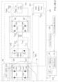
- FIG. 1A illustrates a vehicle system in a charging mode according to at least another example embodiment.
- FIG. 1B illustrates a vehicle system in a traction mode according to at least another example embodiment.
- the vehicle system includes an inverter configured to operate in at least one of a charging mode or a drive mode, a cascaded direct current (DC)-DC converter, the DC-DC converter including a first portion of the inverter and at least one controller configured to selectively couple the first portion of the inverter to a first portion of the cascaded DC-DC converter during the charging mode and selectively couple the inverter to a second portion of the cascaded DC-DC converter during the drive mode.
- the drive mode may also be referred to as a traction mode or a motoring mode.
- the cascaded DC-DC converter includes a first DC-DC converter and a second DC-DC converter and the at least one controller is configured to selectively couple the inverter to the second DC-DC converter during the drive mode.
- the first DC-DC converter is a unidirectional DC-DC converter.
- the first portion of the first DC-DC converter is a single active bridge and the second portion of the first DC-DC converter are two passive bridges.
- the single active bridge is a half-bridge for active switching control and the two passive bridges are two diode bridges for rectification.
- the first DC-DC converter further includes a plurality of diode bridges and a transformer coupled between the diode bridges and the single active bridge.
- the system further includes a first voltage source and a second voltage source, wherein the first DC-DC converter is a first LLC converter having a first inductor connected in series with the first voltage source and the second DC-DC converter is a second LLC converter having a second inductor connected in series with the second voltage source.
- the at least one controller is configured to control the first portion of the inverter during the charging mode based on a DC bus reference voltage.
- the at least one controller includes a proportional-integral-resonant (PIR) controller, a proportional-integral (PI) controller, phase-locked-loop (PLL) controller and a notch filter.
- PIR proportional-integral-resonant
- PI proportional-integral
- PLL phase-locked-loop
- the at least one controller includes a proportional-integral-resonant (PIR) controller and a pulse-frequency-modulation (PFM) controller for the first DC-DC converter.
- PIR proportional-integral-resonant
- PFM pulse-frequency-modulation
- the at least one controller includes a proportional-integral (PI) controller and a pulse-frequency-modulation (PFM) controller for the second DC-DC converter.
- PI proportional-integral
- PFM pulse-frequency-modulation
- the system includes a single-phase AC-DC converter and two cascaded DC/DC converters during the charging mode.
- the charging mode includes a constant current (CC) mode and a constant voltage (CV) mode and the at least one controller is configured to cause the system to operate in a CC mode or CV mode during the charging mode.
- CC constant current
- CV constant voltage
- At least one example embodiment provides a computer-readable medium, when executed by at least one controller, configured to cause a vehicle system to selectively couple a first portion of an inverter to a first portion of a cascaded DC-DC converter during a charging mode, and selectively couple the inverter to a second portion of the cascaded DC-DC converter during a drive mode.
- the computer-readable medium wherein when executed by the at least one controller, is configured to cause the vehicle system to execute a proportional-integral-resonant (PIR) controller, a proportional-integral (PI) controller, phase-locked-loop (PLL) controller and a notch filter.
- PIR proportional-integral-resonant
- PI proportional-integral
- PLL phase-locked-loop
- the computer-readable medium when executed by the at least one controller, is configured to cause the vehicle system to operate in one of a constant current (CC) mode or a constant voltage (CV) mode during the charging mode.
- CC constant current
- CV constant voltage
- the vehicle system includes an inverter configured to operate in at least one of a charging mode or a drive mode, a cascaded direct current (DC)-DC converter, the DC-DC converter including a first portion of the inverter and means for selectively coupling the first portion of the inverter to a first portion of the cascaded DC-DC converter during the charging mode and selectively coupling the inverter to a second portion of the cascaded DC-DC converter during the drive mode.
- DC direct current
- the cascaded DC-DC converter includes a first DC-DC converter and a second DC-DC converter and the vehicle system includes means for selectively coupling the inverter to the second DC-DC converter during the drive mode.
- the vehicle system includes means for controlling the first portion of the inverter during the charging mode based on a DC bus reference voltage.
- the means for controlling includes a proportional-integral-resonant (PIR) controller, a proportional-integral (PI) controller, phase-locked-loop (PLL) controller and a notch filter.
- PIR proportional-integral-resonant
- PI proportional-integral
- PLL phase-locked-loop
- the means for controlling includes a proportional-integral-resonant (PIR) controller and a pulse-frequency-modulation (PFM) controller for the first DC-DC converter.
- PIR proportional-integral-resonant
- PFM pulse-frequency-modulation
- the means for controlling includes a proportional-integral (PI) controller and a pulse-frequency-modulation (PFM) controller for the second DC-DC converter.
- PI proportional-integral
- PFM pulse-frequency-modulation
- the means for controlling is configured to cause the system to operate in a CC mode or CV mode during the charging mode.
- a vehicle system 900 may include a vehicle controller 905, a contactor control circuit 910, an electronic controller 915, a motor 920 and integrated charging and drive control circuitry 930.
- the integrated charging and drive control circuitry 930 may include a filter 935 (e.g., a line filter), a dual purpose inverter 940, a DC-DC output stage 945, a first power supply 950 (e.g., a 350 V battery pack), a converter 952 and a second power supply 954 (e.g., a 12 V battery). While not shown, additional loads may be attached to the converter 952 in parallel with the second power supply 954.
- the dual purpose inverter 940 includes a single inverter. A portion of the dual purpose inverter 940 is configured to operate as part of a cascaded DC-DC converter during the charging mode.
- the vehicle controller 905 controls the contactor control circuit 910 to selectively couple the inverter 940 to the motor during a drive mode (also referred to as the traction mode or a motoring mode), selectively couple the first portion of the inverter to a first portion of the cascaded DC-DC converter during the charging mode, and selectively couple the the inverter to a second portion of the cascaded DC-DC converter during the drive mode.
- a drive mode also referred to as the traction mode or a motoring mode
- the vehicle controller 905 provides a signal to the contactor control circuit 910 to close a switch 960a to connect the AC grid 20 to the filter 935.
- the AC grid 20 provides an input voltage (RMS) of 120 V with an input current (RMS) of 45 A or a voltage of 240 V with a current of 22.5 A.
- RMS input voltage
- RMS input current
- An operator may set a mode signal by selecting the control mode (e.g., charging mode or traction mode) by pushing a button or using an interface such as a touch screen on a vehicle.
- the mode signal indicates whether the vehicle system 900 is to operate in at least one of a charging mode or a traction mode.
- the vehicle controller 905 may select the control mode and set the mode signal based on whether the vehicle system 900 is connected to the grid 20 and whether the motor 920 is running. For example, the vehicle controller 905 may set the mode signal to a charging mode if the vehicle system 900 is connected to the grid 20 and the motor 920 is not running.
- the vehicle controller 905 also provides instructions to the contactor control circuit 910 to close a switch 960b to connect the filter 935 to the dual purpose inverter 940, to close a switch 960c to connect the dual purpose inverter 940 to the DC-DC output stage 945, to close a switch 960d to connect the DC-DC output stage 945 to the first power supply 950, and to operate a switch 960g to connect the DC-DC output stage 945 to the converter 952.
- the vehicle controller 905 and the contactor control circuit 910 collectively operate to open switches 960e and 960f.
- a portion of the dual purpose inverter 940 is configured to operate as an AFE AC-DC converter during the charging mode and a portion of the dual purpose inverter 940 is part of a DC-DC converter during the charging mode. More specifically, two phases (i.e., two half-bridges) of the dual purpose inverter 940 may operate as a single phase AFE converter and one phase (i.e., one half-bridge) may operate as part of a DC-DC converter.
- the vehicle controller 905 provides a signal to the contactor control circuit 910 to close the switch 960e to connect the motor 920 to the dual purpose inverter 940.
- the vehicle controller 905 In a same signal or different signal to the contactor control circuit 910 to close the switch 960e, the vehicle controller 905 also provides instructions to the contactor control circuit 910 to close a switch 960f to connect the dual purpose inverter 940 to the first power supply 950 and to operate the switch 960g to connect the first power supply 950 to the converter 952. In the traction mode, the vehicle controller 905 and the contactor control circuit 910 collectively operate to open switches 960a, 960b, 960c and 960d.
- the first power supply 950 may be a 350 V battery.
- the vehicle controller 905 may be implemented as hardware, such as a processor, firmware or hardware executing software as a special purpose machine.
- vehicle controller 105 When the vehicle controller 105 is hardware, such hardware may include one or more Central Processing Units (CPUs), digital signal processors (DSPs), application-specific-integrated-circuits (ASICs), field programmable gate arrays (FPGAs) computers or the like configured as special purpose machines to perform the functions of described herein.
- CPUs, DSPs, ASICs and FPGAs may generally be referred to as processors and/or microprocessors.
- the vehicle controller 905 is a processor executing software
- the processor is configured as special purpose machine to execute the software to perform the functions of the vehicle controller 905.
- the vehicle controller 905 is a vehicle control unit (VCU).
- VCU vehicle control unit
- the on-board charger allows a user to get power from a utility AC power grid and charge a main 350 V battery in the vehicle, while the 12 V output DC-DC converter could draw power from the main 350V battery and provide power to 12V auxiliary loads, such as a pump, a heater, lighting, and fans.
- the on-board charger and 350-12 V DC-DC converter are usually stand-alone parts. However, those stand-alone parts increase the hardware cost and may occupy more space.
- FIG. 2A illustrates an integrated charging and drive control circuitry in a charging mode according to an example embodiment.
- FIG. 2B illustrates an integrated charging and drive control circuitry in a traction mode according to an example embodiment.
- the integrated charging and drive control circuitry 930 includes the dual purpose inverter 940 and peripheral circuitry 1020.
- the dual purpose inverter 940 is configured for dual purposes: traction drive and for use in a charger.
- existing hardware in an inverter can be reused for an on-board charger.
- hardware costs and system volumes may be reduced because the existing traction inverter is repurposed into a utility cascaded on-board charger with a few additional components.
- the system 900 reduces high-frequency ripples in battery charging currents and the controller 915 reduces the impact of double line-frequency ripples in a AFE DC-link output voltage, which is caused by the single-phase power source (the grid 20) and can deteriorate the charging performance.
- the inverter 940 is disconnected from the motor 920 and re-configured as an AC-DC converter (a single-phase AFE converter) plus a first DC-DC converter 1040 (e.g., a half-bridge LLC converter) to charge the first power supply 950 with the help of switches and passive components (e.g., diodes).
- the converter 952 e.g., a half-bridge LLC converter
- the converter 952 is used to charge the second power supply 954 during the charging mode. In the traction mode shown in FIG.
- the DC/DC output stage 945 includes a resonant tank (C r1 , L r1 , L m1 ), a transformer 1042, a diode bridge, and the DC output capacitor C out1 .
- the DC-DC converter 952 provides power to support the 12 V auxiliary loads in the traction mode.
- the inverter 940 includes half-bridges 1012a, 1012b and 1012c. Each half-bridge includes two switch packages 84 that are placed across a DC-link 942. Each switch package 84 includes a diode 84-1 and a MOSFET transistor 84-2.
- One switch package 84 in each half-bridge is a top-side 985 of the half-bridge and the other switch package 84 is a bottom side 990 of the half-bridge.
- the transistor 84-2 When the appropriate voltage is applied to the gate of an MOSFET transistor 84-2, the transistor 84-2 may be activated and the drain may be coupled electrically to the emitter to supply electric power.
- the appropriate voltage depends on a rating of the transistor 84-2. For example, 14 V may be applied at the gate to turn the transistor 84-2 on. Negative 8 V may be applied at the gate with to turn the transistor 84-2 off.
- MOSFET transistors are shown, field effect transistors, complementary metal oxide semiconductors, power transistors, or other suitable semiconductor devices may be used.
- switch states indicate whether a properly functioning or unimpaired semiconductor device is active ("on” or “closed”) or inactive (“off' or “open”).
- a failure of a semiconductor device to change states may result in a semiconductor device failing in an open state or a closed state, for example.
- the controller 915 may have gate drivers 50, a microprocessor 52 coupled electrically to the gate drivers 50, and memory 54 coupled electrically to the microprocessor 52 and having stored therein operating instructions for the microprocessor 52.
- the gate of each transistor 84-2 is coupled electrically to a respective gate driver 50 that is dedicated to that transistor 84-2 and may provide a DC voltage (e.g., 14 V DC) to turn on and off that transistor 84-2.
- a gate driver 50 for each transistor 84-2 there may be a gate driver 50 for each transistor 84-2.
- the gate drivers 50 for the transistor 84-2 are under the control of the microprocessor 52, which may employ a pulse-frequency-modulation (PFM) (or pulse-width-modulation (PWM)) control scheme to control those gate drivers 50 and the transistor 84-2 to supply electric energy to the DC-link 942 in the charging mode and remove electric energy from the DC-link 942 in the traction mode.
- PFM pulse-frequency-modulation
- PWM pulse-width-modulation
- the DC-link 942 may have a high rating, for example, 700V, and a capacitance C dc determined based on the inverter design and applications' requirements.
- the capacitance C dc is 1000 ⁇ F.
- the filter 935 includes an inductor 1005.
- a first end of the inductor 1005 is connected to the grid 20 and a second end of the inductor 1005 is connected between the switch packages 84 of the half-bridge 1012a (i.e., between a source of the MOSFET of high side switch package 84 and a drain of the MOSFET of the low side switch package 84).
- the inductor 1005 may have an inductance of 300 ⁇ H, and the zero-crossing frequency of the L filter is about 530 Hz.
- filter 935 is illustrated as an L filter, it should be understood that other filters may be used such as an LR filter or an LCL filter.
- the output of the filter 935 (the second end of the inductor 1005) is input to a single-phase AFE converter 1030.
- the single-phase AFE converter 1030 includes the half-bridges 1012a and 1012b.
- the single-phase AFE converter 1030 receives pulse-width modulated signals from the controller 915 to convert the AC voltage output from the grid 20 to DC voltage through the filter 935.
- the switching frequency of the transistors 84-2 in the AFE converter 1030 may be 15 kHz.
- the single-phase AFE converter 1030 outputs a voltage V AFE to the DC-link 942.
- other power switches such as IGBTs may be used instead of MOSFETS.
- a DC-DC converter 1040 includes the half-bridge 1012c, a capacitor C r1 , and inductor L r1 , a transformer 1042, a diode bridge 1044 and an output capacitor C out1 .
- the diode bridge 1044 includes diodes 1046-1049. Diodes may be considered passive components.
- a first end of the capacitor C r1 is connected between the switch packages 84 of the half-bridge 1012c (i.e., between a source of the MOSFET of a high side switch package 1012c1 of the half-bridge 1012c and a drain of the MOSFET of a low side switch package 1012c2 of the half-bridge 1012c).
- a second end of the capacitor C r1 is connected to a first end of a primary side of the transformer 1042.
- a first end of the inductor L r1 is connected to a low-side rail of the inverter 940 and a source of the MOSFET of the low side switch package 84 of the half-bridge 1012c.
- a second end of the inductor L r1 is connected to a second end of the primary side of the transformer 1042.
- a first end of a secondary side of the transformer 1042 is connected between the diodes 1046 and 1047.
- a second end of the secondary side of the transformer 1042 is connected between the diodes 1048 and 1049.
- First ends of the diodes 1046 and 1048 are connected to a node N3.
- a second end of the diode 1046 is connected to a first end of the diode 1047 (and the first end of the secondary side of the transformer 1042).
- a second end of the diode 1048 is connected to a first end of the diode 1049 (and the second end of the secondary side of the transformer 1042).
- the output capacitor C out1 has a first end connected to the node N3 and a second end connected to the node N2.
- the converter 952 provides power to the second power supply 954 and other loads and may be a unidirectional DC-DC converter.
- the converter 952 is connected to the converter 1040 at nodes N2 and N3.
- the input voltage for the second converter 952 is the output of the converter 1040 (i.e., a voltage across C out1 ).
- the converter 952 includes an active halfbride 1052, a capacitor C r2 , and inductor L r2 , a transformer 1054, a diode bridge 1056 and an output capacitor C out2 .
- the diode bridge 1056 includes diodes 1062-1065.
- the converter 952 may include an inductor L bat2 is included.
- the inductor L bat2 may be considered a cable impedance or extra inductor.
- the active half-bridge 1052 includes a high side switch package 1060a and a low side switch package 1060b.
- the high side switch package 1060a and the low side switch package 1060b are structured in the same manner as the high side and low side switch packages 84.
- a drain of the MOSFET of the high side switch package 1060a is connected to the node N2.
- a source of the MOSFET of the low side switch package 1060b is connected to the node N3.
- a first end of the capacitor C r2 is connected between the high side switch package 1060a and the low side switch package 1060b (i.e., between a drain of the MOSFET of the low side switch package 1060b and a source of the MOSFET of the high side switch package 1060a).
- a second end of the capacitor C r2 is connected to a first end of a primary side of the transformer 1054.
- a first end of the inductor L r2 is connected to source of the MOSFET of the low side switch package 1060b and the node N3.
- a second end of the inductor L r2 is connected to a second end of the primary side of the transformer 1054.
- a first end of a secondary side of the transformer 1054 is connected between the diodes 1062 and 1063.
- a second end of the secondary side of the transformer 1054 is connected between the diodes 1064 and 1065.
- First ends of the diodes 1062 and 1064 are connected to a node N4.
- a second end of the diode 1062 is connected to a first end of the diode 1063 (and the first end of the secondary side of the transformer 1054).
- a second end of the diode 1064 is connected to a first end of the diode 1065 (and the second end of the secondary side of the transformer 1054).
- the output capacitor C out2 has a first end connected to the node N4 and a second end connected to the node N5. While only one output capacitor C out2 is shown, it should be understood that each 12 V load may have its own input capacitor.
- the inductor L bat2 includes a first end connected to the node N5 and a second end connected to the power supply 954.
- An inductor L bat1 has a first end connected to the node N2 and a second end connected to a positive terminal of the first power supply 950. A negative terminal of the first power supply 950 is connected to the node N3.
- the inductor Lbat1 reduces the charging current ripple.
- a positive terminal of the second power supply 954 is connected to the node N5 and a negative terminal of the second power supply 954 is connected to the node N4.
- Both the converter 1040 and the converter 952 have the same structure and may be considered LLC converters.
- FHA first-harmonic-approximation
- L r i.e., L r1 or L r2
- L m i.e., Lm1 or Lm2
- C r i.e., C r1 or C r2
- n is the transformer turns ratio
- R ac 8 n 2 ⁇ 2
- R load is an equivalent ac load resistance at the switching frequency of the high side switch package of the converter
- R load is the actual load resistance
- the voltage V in is the voltage across the DC-link 942 (i.e., output voltage of the AFE converter 1030) and V out is the voltage across the capacitor C out1 .
- the voltage V in is the voltage across the capacitor C out1 and V out is the voltage across the capacitor C out2 (i.e., the voltage V ba2 ).
- the converter 1040 may achieve zero voltage switching (ZVS) operation in the primary side of the transformer 1042 and DCM operation on the secondary side of the transformer 1042 if the switching frequency of the switch package 1012c1/c2 is within a range [ ⁇ 2 , ⁇ 1 ].
- the converter 952 may achieve zero voltage switching (ZVS) operation in the primary side of the transformer 1054 and DCM operation on the secondary side of the transformer 1054 if the switching frequency of the switching packages 1060a /b is within a range [ ⁇ 2 , ⁇ 1 ].
- the converter 1040 may be controlled such that the high side switch (or top switch), and the bottom switch operate in a complementary mode (top/bottom: ON/OFF or top/bottom: OFF/ON).
- the converter 952 may be controlled such that the high side switch (or top switch), and the bottom switch operate in a complementary mode (top/bottom: ON/OFF or top/bottom: OFF/ON).
- the voltage gain conditions for the converters 1040 and 952 may be 2 nV out V in , max ⁇ 1 > 1 a 2 nV out V in , min ⁇ 2 ⁇ m m + 1 m 2 Q b where V in,min is the minimal input voltage of the applicable LLC converter, and V in,max is the maximum input voltage of the applicable LLC converter.
- a current sensor 296 may be used to detect the zero-crossing point of the currents I sec1 and Isec2 .
- the current sensor provides current measurements to the controller 915.
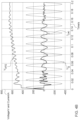
- FIG. 3 illustrates current waveforms of the converter 1040 according to at least one example embodiment.
- a capacitance Cdc of the DC-link 942 is 1000 ⁇ F and inductance of the inductor L bat in the converter 1040 is .5 ⁇ H.
- FIG. 3 illustrates a gating signal G top1 , a power source current I bat1 (also shown in FIG. 2A ), a magnetizing current I m1 , a primary side current I pri1 (also shown in FIG. 2A ) and a secondary side current I sec1 (also shown in FIG. 2A ).
- the magnetizing current I m1 is the magnetizing current of the transformer 1042.
- the gate signal G to1p controls the high-side transistor of the half-bridge 1012c.
- control methods and design of the converter 1040 described with reference to FIG. 3 are also applicable to the converter 952.
- the subscript "1" or "2" is omitted to indicate that the control method applies to both the converter 1040 and the converter 952 (they may be controlled independently) except when referring specifically to what is shown in FIG. 3 .
- the primary side current I pri is negative, thus, ZVS could be achieved if the power device is an ideal switch, as the current flows through the body-diode of the high side switch (e.g., diode of switch package 1012c1 and diode of the switching package 1060a) during the deadtime.
- the body-diode of the high side switch e.g., diode of switch package 1012c1 and diode of the switching package 1060a
- both IGBT and MOSFET transistors have an output capacitance C oss which is caused by the physical structure of the junction. Due to the existence of the capacitance C oss , when the low side switch is off, the primary side current may not directly flow through the body-diode of the high side switch.
- the primary side current I pri discharges the capacitance C oss first, as the top switch voltage is clamped by the capacitance C oss and prevents/restricts the current flowing through the high side body-diode.
- the primary side current I pri discharges the capacitance C oss during a deadtime T dead .
- the primary side current I pri1 is the same as the magnetizing current I m1 , as the secondary side current I sec1 is zero (DCM operation).
- the converter 1040 has a resonant frequency ⁇ 1 of 20 kHz, m is 10, and the transformer turns ratio is 0.9625 for 400 V output and 770 V input.
- an upper limit of the quality factor Q may be: Q ⁇ m m + 1 m 2 V in , min 2 nV out .
- the quality factor Q may be 95% of the upper limit, and the equivalent ac load resistance at the switching frequency R ac may be calculated at the highest output power.
- the leakage inductance L r is set as 10.9 uH
- the capacitance C r is 5.8 uF
- the inductance L m is 109.5 uH for the converter 1040.
- the designs of the converters 1040 and 952 may be performed in the same manner.
- the required components are the same.
- both LLC converters needs transformer, inductor, and capacitor.
- the values of the transformer, the inductor, and the capacitor are different between the converters 1040 and 952 since the converters 1040 and 952 may have different voltage and power ratings.
- the controller 915 may include separate controllers for the AFE converter 1030 (a controller 1200), the converter 1040 (a controller 1300) and the converter 952 (a controller 1400).
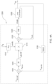
- FIG. 4A illustrates at least one example embodiment of an AFE controller.
- an AFE controller 1200 may include a subtractor 1202, a proportion integral (PI) controller 1205, a phase-locked-loop (PLL) controller 1210, a multiplier 1215, a subtractor 1220, a proportion-integral-resonant (PIR) controller 1225 and a notch filter 1230.
- the AFE controller 1200, including the subtractor 1202, the proportion integral (PI) controller 1205, the phase-locked-loop (PLL) controller 1210, the multiplier 1215, the subtractor 1220, the proportion-integral-resonant (PIR) controller 1225 and the notch filter 1230 may be implemented as hardware, such as a processor, firmware or hardware executing software as a special purpose machine.
- Such hardware may include one or more Central Processing Units (CPUs), digital signal processors (DSPs), application-specific-integrated-circuits (ASICs), field programmable gate arrays (FPGAs) computers or the like configured as special purpose machines to perform the functions of the subtractor 1202, the proportion integral (PI) controller 1205, the phase-locked-loop (PLL) controller 1210, the multiplier 1215, the subtractor 1220, the proportion-integral-resonant (PIR) controller 1225 and the notch filter 1230.
- CPUs, DSPs, ASICs and FPGAs may generally be referred to as processors and/or microprocessors.
- the processor is configured as special purpose machine to execute the software to perform the functions of the AFE controller 1200.
- C dc is the output capacitance of the AFE converter, i.e., the dc-link capacitance
- V max and V min are the AFE output voltage maximum and minimal values respectively
- V avg is the average output voltage of the AFE converter 1030.
- the average output voltage V avg may be measured using a voltage sensor (e.g., the voltage sensor 298, and averaging the measured voltage during one wave cycle at the fundamental frequency of the grid (e.g., 60Hz).
- the output voltage ripple is about ⁇ 23 V if the average output voltage of the AFE converter 1030 is 657 V.
- a virtual d-q frame control may be used to control the output voltage of the AFE converter 1030.
- An outer loop of the controller 1200 is a voltage loop to regulate the output voltage of the AFE converter 1030.
- the subtractor generates a difference between a DC-link reference voltage V dc-ref and a filtered dc-link voltage V dc-filt .
- the PI controller 1205 receives the difference the DC-link reference voltage V dc-ref and the filtered dc-link voltage V dc-filt and generates I Lac-ref .
- the reference voltage V dc-ref may be based on empirical data and preprogrammed. In some example embodiments, the reference voltage V dc-ref may be constant and in other example embodiments, the reference voltage V dc-ref may change based on the input voltage to the AFE converter 1030.
- the PLL controller 1210 generates a sin( ⁇ ) output based on a grid voltage u g .
- the grid voltage grid voltage u g includes two types of information: amplitude and phase where ⁇ is the phase information of the grid voltage u g .
- the multiplier 1215 multiplies I Lac-ref by sin( ⁇ ).
- the subtractor 1220 determines a difference between the product generated by the multiplier and I Lac .
- the difference determined by the subtractor 1220 is input to the PIR controller 1225.
- the PIR 1225 uses the difference determined by the subtractor 1220, the PIR 1225 generates pulse-width-modulation (PWM) signals to the AFE converter 1030.
- PWM pulse-width-modulation
- Measurements of the dc-link voltage V dc (voltage of DC-link 942) and the current I Lac are inputs into the AFE controller 1200.
- the notch filter 1230 filters the dc-link voltage V dc to generate the filtered dc-link voltage V dc-filt .
- the notch filter 1230 may be used to reduce a sensitivity of the controller 1200 to the output double line-frequency ripples.
- ⁇ filt is a notch frequency (e.g., 120 Hz)
- ⁇ 1 and ⁇ 2 are damping ratios.
- a depth and a width of the notch filter 1230 are controlled by the selection of the damping ratios ⁇ 1 and ⁇ 2 .
- the damping ratios ⁇ 1 and ⁇ 2 may be determined based on a desired width and depth of the notch filter 1230.
- the PLL controller 1210 is used to obtain phase information of the AC grid voltage. This permits the reference AC current I Lac-ref ⁇ sin( ⁇ ) to be in phase with the grid voltage by multiplying I Lac-ref by sin( ⁇ ) for the unity power factor control.
- the proportional-integral-resonant (PIR) controller 1225 is used to track the reference AC current I Lac-ref ⁇ sin( ⁇ ) (e.g., a 60 Hz current), as the resonant control term of the PIR controller 1225 may increase a controller gain at the resonant frequency, and thus, the tracking error at the resonant frequency will be reduced.
- I Lac-ref ⁇ sin( ⁇ ) e.g., a 60 Hz current
- K p and K i are gains of the PIR controller 1225
- K r is the gain of the resonant term
- ⁇ res is the resonant frequency, which is 60Hz in the PIR controller 1225
- ⁇ res is the damping ratio of the resonant term.
- the gains K p , K i and K r and the damping ratio ⁇ res are determined based on empirical data and/or frequency-domain design techniques such as stability margin analysis.
- the controller 915 determines the gain of the resonant term K r /2 ⁇ res , so both decreasing the damping ratio ⁇ res or increasing the gain K r may improve the tracking accuracy.
- a power factor can be controlled by adding an offset on the grid phase information sin( ⁇ ). Then, the reference AC current I Lac-ref ⁇ sin(S) will be shifted. For example, by adding 30 degrees phase offset to the output of the PLL controller 1210, the power factor can be changed to 0.866.
- the AFE controller 1200 implements a variable AFE output voltage scheme to help the converter 1040 narrow down an operating frequency range.
- a variable AFE reference voltage scheme is discussed in Li et al, "A 300-kHz 6.6-kW SiC Bidirectional LLC Onboard Charger," in IEEE Transactions on Industrial Electronics, vol. 67, no. 2, pp. 1435-1445, Feb. 2020, doi: 10.1109/TIE.2019.2910048 , the entire contents of which are hereby incorporated by reference.
- the reference output voltage V dc-ref of the AFE converter 1030 is also changed from 480 V to 650 V based on the power source voltage V bat1 .
- the converter 1040 may deal with an almost constant input and output voltage ratio, ignoring the voltage ripples, and the operating switching frequency range can be narrowed down accordingly.
- FIG. 4B illustrates a timing diagram of the output voltage V AFE , the current I Lac and u g , according to an example embodiment. As shown, a variable AFE output voltage V AFE is implemented.
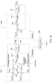
- FIGS. 5A-5B illustrate at least one example embodiment of a controller for the converter 1040.
- the converter controller 1300 includes a subtractor 1302, a subtractor 1304, a PIR controller 1305, a PIR controller 1310, a switch 1312 and a pulse-frequency modulation (PFM) generator 1320.
- the converter controller 1300, including the subtractor 1302, the subtractor 1304, the PIR controller 1305, the PIR controller 1310, the switch 1312 and the PFM generator 1320 may be implemented as hardware, such as a processor, firmware or hardware executing software as a special purpose machine.
- Such hardware may include one or more Central Processing Units (CPUs), digital signal processors (DSPs), application-specific-integrated-circuits (ASICs), field programmable gate arrays (FPGAs) computers or the like configured as special purpose machines to perform the functions of the subtractor 1302, the subtractor 1304, the PIR controller 1305, the PIR controller 1310, the switch 1312 and the PFM generator 1320.
- CPUs, DSPs, ASICs and FPGAs may generally be referred to as processors and/or microprocessors.
- the converter controller 1300 may operate as a constant voltage (CV) charging controller or a constant current (CC) charging controller based on a charging mode selection signal. As will be shown and described with reference to FIG. 5B , the converter controller 1300 may operate in one of the CV or CC mode based on a state-of-charge (SOC) of the power supply 950. For example, when the SOC is relatively low (e.g., less than 90%), the CC mode is used to charge the power supply 950 with a constant charging current. When the state-of-charge is relatively high (e.g., above 90%), CV mode may be used.
- SOC state-of-charge
- the subtractor 1302 determines a difference between a power source reference voltage V bat1-ref and the converter output voltage V bat1 .
- the power source reference voltage V bat1-ref may be equal to (or substantially similar) to a battery open-circuit voltage when the battery state-of-charge is 100%, i.e., fully charged.
- the PIR controller 1305 generates a switching frequency F SW1 (described above with reference to FIG. 3 ) based on the difference determined by the subtractor 1302 and applies the switching frequency F SW1 to the PFM generator 1320.
- the PFM generator 1320 generates the top side gate signal G top1 (as described above and shown in FIG. 3 ).
- the gate signal to control the bottom side of the switch package e.g., 1012c2
- the gate signal to control the bottom side of the switch package may be in a complementary mode with respect to the top side gate signal G top1 .
- both the top side gate signal G top1 and the gate signal to control the bottom side of the switch package are off (e.g., 0 V or logic low).
- the subtractor 1304 determines a difference between a power source reference current I bat1-ref and the converter output current I bat1 .
- the power source reference current I bat1-ref may be a set value and based on a datasheet of the power supply 950.
- the PIR controller 1310 generates the switching frequency F SW1 based on the difference determined by the subtractor 1304 and applies the switching frequency F SW1 to the PFM 1320.
- the PFM generates the top side gate signal G top1 (as described above and shown in FIG. 3 ).
- the PIR controllers 1305, 1310 are used to provide voltage tracking and current tracking, respectively.
- the PIR controllers 1305, 1310 receive a voltage tracking error (V bat1-ref - V bat1 ) and a current tracking error (I bat1-ref - I bat1 ), respectively, then generate a corresponding switching frequency Fsw to reduce the tracking error and attempt to remove the tracking error.
- the PFM generator 1320 applies the top side gate signal G top1 as well as the gate signal to control the bottom side of the switch package to the converter 1040.
- the power source reference current I bat1-ref and the power source reference voltage V bat1-ref signals, as well as the charging mode selection signal, may be obtained from a battery-management-system (BMS).
- BMS battery-management-system
- An example BMS includes AN1086 Orion BMS, but is not limited thereto.
- the converter 1040 may operate in the DCM mode, and the voltage relationship between the input and output voltages is nonlinear.
- the controller 1300 uses a feedforward term to improve a dynamic response of the converter 1040 and compensate for the nonlinearity.
- the output voltage of AFE converter 1030 i.e., the input voltage of the converter 1040, may contain double line-frequency ripples.
- the PIR controllers 1305 and 1310 are used to attenuate an impact of input double line-frequency voltage ripples, and the resonant frequency of the controller 1300 is set as the double line-frequency (e.g. 120 Hz) to reject the input voltage ripple.
- the double line-frequency e.g. 120 Hz
- the converter controller 1300 operates based on an activation signal and the mode signal generated by the controller 915. More specifically, and as shown in FIG. 5B , the controller 915 monitors the voltage V dc across the DC-link 942 using a voltage sensor 298. The controller 915 controls the AFE converter 1030 to charge the DC-link 942. Once the controller 915 determines the voltage V dc reaches a threshold level (e.g., becomes relatively stable) in the charging mode, the controller 915 generates the activation signal to enable the converter 1040 to operate and charge the power source 950.
- a threshold level e.g., becomes relatively stable
- FIG. 5B illustrates an operation of the vehicle system 900 in the charging mode.
- the vehicle system 900 operates in an AFE charging period until a time T 1 (e.g., when the DC-link voltage V dc reaches a threshold level).
- a time T 1 e.g., when the DC-link voltage V dc reaches a threshold level.
- the AFE converter 1030 generates a voltage at the DC-link 942.
- the converter controller 1300 causes the converter 1040 to operate in a CC mode.
- the AFE converter 1030 may continue to operate in a same manner to maintain the DC-link voltage V dc .
- the converter 1040 switches to the CV mode when the SOC reaches a threshold percentage.
- a voltage sensor may provide feedback to the controller 1300, and the SOC can be calculated based on the battery terminal voltage measured through the voltage sensor.
- the controller 1300 may generate the charging mode selection signal (shown in FIG. 5A ) based on whether the SOC exceeds the threshold level.
- the threshold of the SOC may be 95%.
- the CV mode causes the current I bat1 to decrease such that the power source voltage V bat1 remains constant.
- FIGS. 6A-6C illustrate at least one example embodiment of a controller for the converter 952.
- the converter controller 1400 includes a charging portion 1400a and a traction portion 1400b.
- the charging portion 1400a includes a subtractor 1402, a subtractor 1404, a PI controller 1405, a PI controller 1410, a switch 1412 and a pulse-frequency modulation (PFM) generator 1420.
- the charging portion 1400a, including the subtractor 1402, the subtractor 1404, the PI controller 1405, the PI controller 1410, the switch 1412 and the PFM generator 1420 may be implemented as hardware, such as a processor, firmware or hardware executing software as a special purpose machine.
- such hardware may include one or more Central Processing Units (CPUs), digital signal processors (DSPs), application-specific-integrated-circuits (ASICs), field programmable gate arrays (FPGAs) computers or the like configured as special purpose machines to perform the functions of the subtractor 1402, the subtractor 1404, the PI controller 1405, the PI controller 1410, the switch 1412 and the PFM generator 1420.
- CPUs, DSPs, ASICs and FPGAs may generally be referred to as processors and/or microprocessors.
- the traction portion 1400b includes a subtractor 1452, a PI controller 1455 and a PFM 1460.
- the PFM 1460 may be the same as the PFM generator 1420.
- the traction portion 1400b, including the subtractor 1452, the PI controller 1455 and the PFM 1460 may be implemented as hardware, such as a processor, firmware or hardware executing software as a special purpose machine.
- such hardware may include one or more Central Processing Units (CPUs), digital signal processors (DSPs), application-specific-integrated-circuits (ASICs), field programmable gate arrays (FPGAs) computers or the like configured as special purpose machines to perform the functions of the subtractor 1452, the PI controller 1455 and the PFM 1460.
- CPUs, DSPs, ASICs and FPGAs may generally be referred to as processors and/or microprocessors.
- the converter controller 1400 further includes a selection circuit 1465 that selects one of the charging portion 1400a and the traction portion 1400b based on the model signal.
- the converter controller 1400 activates the charging portion 1400a when the activation signal indicates a CC or CV mode (e.g., when the DC-link voltage V dc reaches a threshold level).
- the converter controller 1400 activates the traction portion 1400b when the mode signal indicates the traction mode.
- the converter controller 1400 may operate as a constant voltage (CV) charging controller or a constant current (CC) charging controller in the charging mode based on a charging mode selection signal. As will be shown and described with reference to FIG. 6B , the converter controller 1400 may operate in one of the CV or CC mode based on a state-of-charge (SOC) of the power supply 954. For example, when the SOC is relatively low (e.g., less than 90%), the CC mode is used to charge the power supply 954 with a constant charging current. When the state-of-charge is relatively high (e.g., above 90%), CV mode may be used.
- SOC state-of-charge
- the subtractor 1402 determines a difference between a power source reference voltage V bat2-ref and the converter output voltage V bat2 .
- the power source reference voltage V bat2-ref may be equal to (or substantially similar) to a battery open-circuit voltage when the battery state-of-charge is 100%, i.e., fully charged.
- the switch 1412 operationally connects the PI controller 1405 to the PFM generator 1420.
- the PI controller 1405 generates a switching frequency F SW2 (determined in accordance with the description above with reference to FIG. 3 ) based on the difference determined by the subtractor 1402 and applies the switching frequency F SW2 to the PFM generator 1420.
- the PFM generator 1420 generates a top side gate signal G top2 (as described above and shown in FIG. 6B ).
- the switch 1412 operationally connects the PI controller 1410 to the PFM generator 1420.
- the subtractor 1404 determines a difference between a power source reference current I bat2-ref and the converter output current I bat2 .
- the power source reference current I bat2-ref may be a set value and based on a datasheet of the power supply 954.
- the PI controller 1410 generates the switching frequency F SW2 based on the difference determined by the subtractor 1404 and applies the switching frequency F SW2 to the PFM generator 1420.
- the PFM generator 1420 generates the top side gate signal G top2 (as described above and shown in FIG. 6B ).
- the PI controllers 1405, 1410 are used to provide voltage tracking and current tracking, respectively.
- the PI controllers 1405, 1410 receive a voltage tracking error (V bat2-ref - V bat2 ) and a current tracking error (I bat2-ref - I bat2 ), respectively, then generate a corresponding switching frequency F SW2 to reduce the tracking error and attempt to remove the tracking error.
- V bat2-ref - V bat2 a voltage tracking error
- I bat2-ref - I bat2 current tracking error
- the PFM generator 1420 applies the top side gate signal G top2 to the converter 952.
- the PFM generator 1420 generates the top side gate signal G top2 (as shown in FIG. 6B ).
- the gate signal to control the bottom side of the switch package e.g., 1060b
- the gate signal to control the bottom side of the switch package may be in a complementary mode with respect to the top side gate signal G top2 .
- both the top side gate signal G top2 and the gate signal to control the bottom side of the switch package are off (e.g., 0 V or logic low).
- the power source reference current I bat2-ref and the power source reference voltage V bat2-ref signals, as well as the charging mode selection signal, may be obtained from a battery-management-system (BMS).
- BMS battery-management-system
- An example BMS includes AN1086 Orion BMS, but is not limited thereto.
- FIG. 6B illustrates current waveforms of the converter 952 according to at least one example embodiment.
- a power source current I bat2 is a power source current of the power supply 954, a magnetizing current I m2 is the magnetizing current of the transformer 1054, the primary side current I pri2 is the primary side current of the transformer 1054 and the secondary side current I sec2 is the secondary side current of the transformer 1054.
- the gate signal G top2 controls the transistor of the high side switch package 1060a. ZVS occurs at times T 1 , T 2 and T 3 , for example.
- the converter 952 may operate in the DCM mode, and the voltage relationship between the input and output voltages is nonlinear.
- the controller 1400 uses a feedforward term to improve a dynamic response of the converter 952 and compensate for the nonlinearity.
- the charging portion 1400a operates based on the activation and mode signals generated by the controller 915. More specifically, and as shown in FIG. 6C , the controller 915 monitors the voltage Vdc across the DC-link 942 using the voltage sensor 298. The controller 915 controls the AFE converter 1030 to charge the DC-link 942. Once the controller 915 determines the voltage V dc reaches a threshold level (e.g., becomes relatively stable) in the charging mode, the controller 915 generates the activation signal to enable both the converter 1040 and the converter 952 to operate and charge the power supply 954.
- a threshold level e.g., becomes relatively stable
- FIG. 6C illustrates an operation of the vehicle system 900 in the charging mode.
- the vehicle system 900 operates in an AFE charging period until a time T 1 (e.g., when the DC-link voltage V dc reaches a threshold level).
- a time T 1 e.g., when the DC-link voltage V dc reaches a threshold level.
- the AFE converter 1030 generates a voltage at the DC-link 942.
- the converter controller 1400 causes the converter 952 to operate in a CC mode.
- the AFE converter 1030 may continue to operate in a same manner to maintain the DC-link voltage V dc , and the converter 1040 maintains the DC output voltage across the capacitor C out1 , which is the input voltage of the converter 952.
- the converter 952 switches to the CV mode when the SOC reaches a threshold percentage.
- a voltage sensor may provide feedback to the controller 1400, and the SOC can be calculated based on the battery terminal voltage measured through the voltage sensor.
- the controller 1400 may generate the charging mode selection signal (shown in FIG. 6A ) based on whether the SOC exceeds the threshold level.
- the threshold of the SOC may be 95%.
- the CV mode causes the current I bat2 to decrease such that the power source voltage V bat2 remains constant.
- each switch package 84 is switched on and off to generate the three phases from the DC-link 942 to the motor 920.
- the switch packages 84 of the inverter 940 are switched on and off to generate the three phases for the motor 920.
- the DC/DC output stage 945 and the filter 935 become operably disconnected from the inverter 940 with the exception of the output capacitor C out1 .
- the first end of the capacitor C out1 , the first end of the inductor Lbat1, a positive terminal of the power supply 950, and the high side switch package 84 of the converter 952 become connected to a high side rail of the inverter 940 at a node N6.
- a first end of the inductor L r2 , a negative terminal of the power supply 950, and the low side switch package 84 of the converter 952 become connected to a low side rail of the inverter 940 at a node N7.
Landscapes
- Engineering & Computer Science (AREA)
- Power Engineering (AREA)
- Transportation (AREA)
- Mechanical Engineering (AREA)
- Life Sciences & Earth Sciences (AREA)
- Sustainable Development (AREA)
- Sustainable Energy (AREA)
- Dc-Dc Converters (AREA)
Abstract
Description
- Example embodiments are related to drive systems and charger systems such as dual-purpose drive and charger systems.
- In a conventional electric vehicle, an on-board charger is usually a stand-alone part, which means that the manufacturer needs to purchase or design a fully functional stand-alone on-board charger and install it on the vehicle.
- The stand-alone on-board charger will increase the hardware cost. Meanwhile, the stand-alone charger will also occupy extra space inside the vehicle.
- At least some example embodiments provide an integrated on-board charger that reduces the hardware cost and system volume compared to conventional systems. Moreover, an on-board charger solution according to at least some example embodiments reduces charging current ripples by utilizing combined control techniques, such as proportional integral resonant (PIR) control, phase locked control, pulse-frequency-modulation (PFM) control techniques, along with double line frequency ripple reduction.
- At least one example embodiment includes, a system includes an inverter configured to operate in at least one of a charging mode or a drive mode, a cascaded direct current (DC)-DC converter, the DC-DC converter including a first portion of the inverter and at least one controller configured to selectively couple the first portion of the inverter to a first portion of the cascaded DC-DC converter during the charging mode, and selectively couple the first portion of the inverter to a second portion of the cascaded DC-DC converter during the drive mode.
- Example embodiments will be more clearly understood from the following detailed description taken in conjunction with the accompanying drawings.
FIGS. 1-6C represent non-limiting, example embodiments as described herein. -
FIG. 1A illustrates a vehicle system in a charging mode according to at least one example embodiment; -
FIG. 1B illustrates a vehicle system in a traction mode according to at least one example embodiment; -
FIG. 2A illustrates an integrated charging and drive control circuitry in a charging mode according to at least one example embodiment; -
FIG. 2B illustrates an integrated charging and drive control circuitry in a traction mode according to at least one example embodiment; -
FIG. 3 illustrates current waveforms of an LLC converter shown inFIG. 2A according to at least one example embodiment; -
FIGS. 4A-4B illustrate at least one example embodiment of an AFE (Active Front End) controller; -
FIGS. 5A-5B illustrate at least one example embodiment of a controller for a DC/DC converter; and -
FIGS. 6A-6C illustrate at least one example embodiment of a controller for another DC/DC converter. - Some example embodiments will now be described more fully with reference to the accompanying drawings in which some example embodiments are illustrated.
- Accordingly, while example embodiments are capable of various modifications and alternative forms, embodiments thereof are shown by way of example in the drawings and will herein be described in detail. It should be understood, however, that there is no intent to limit example embodiments to the particular forms disclosed, but on the contrary, example embodiments are to cover all modifications, equivalents, and alternatives falling within the scope of the claims. Like numbers refer to like elements throughout the description of the figures.
- It will be understood that, although the terms first, second, etc. may be used herein to describe various elements, these elements should not be limited by these terms. These terms are only used to distinguish one element from another. For example, a first element could be termed a second element, and, similarly, a second element could be termed a first element, without departing from the scope of example embodiments. As used herein, the term "and/or" includes any and all combinations of one or more of the associated listed items.
- It will be understood that when an element is referred to as being "connected" or "coupled" to another element, it can be directly connected or coupled to the other element or intervening elements may be present. In contrast, when an element is referred to as being "directly connected" or "directly coupled" to another element, there are no intervening elements present. Other words used to describe the relationship between elements should be interpreted in a like fashion (e.g., "between" versus "directly between," "adjacent" versus "directly adjacent," etc.).
- The terminology used herein is for the purpose of describing particular embodiments only and is not intended to be limiting of example embodiments. As used herein, the singular forms "a," "an" and "the" are intended to include the plural forms as well, unless the context clearly indicates otherwise. It will be further understood that the terms "comprises," "comprising," "includes" and/or "including," when used herein, specify the presence of stated features, integers, steps, operations, elements and/or components, but do not preclude the presence or addition of one or more other features, integers, steps, operations, elements, components and/or groups thereof.
- It should also be noted that in some alternative implementations, the functions/ acts noted may occur out of the order noted in the figures. For example, two figures shown in succession may in fact be executed substantially concurrently or may sometimes be executed in the reverse order, depending upon the functionality/acts involved.
- Unless otherwise defined, all terms (including technical and scientific terms) used herein have the same meaning as commonly understood by one of ordinary skill in the art to which example embodiments belong. It will be further understood that terms, e.g., those defined in commonly used dictionaries, should be interpreted as having a meaning that is consistent with their meaning in the context of the relevant art and will not be interpreted in an idealized or overly formal sense unless expressly so defined herein.
- Portions of example embodiments and corresponding detailed description are presented in terms of software, or algorithms and symbolic representations of operation on data bits within a computer memory. These descriptions and representations are the ones by which those of ordinary skill in the art effectively convey the substance of their work to others of ordinary skill in the art. An algorithm, as the term is used here, and as it is used generally, is conceived to be a self-consistent sequence of steps leading to a result. The steps are those requiring physical manipulations of physical quantities. Usually, though not necessarily, these quantities take the form of optical, electrical, or magnetic signals capable of being stored, transferred, combined, compared, and otherwise manipulated. It has proven convenient at times, principally for reasons of common usage, to refer to these signals as bits, values, elements, symbols, characters, terms, numbers, or the like.
- In the following description, illustrative embodiments will be described with reference to acts and symbolic representations of operations (e.g., in the form of flowcharts) that may be implemented as program modules or functional processes including routines, programs, objects, components, data structures, etc., that perform particular tasks or implement particular abstract data types and may be implemented using existing hardware.
- Such existing hardware (e.g., data processors and controllers) may be implemented using processing or control circuitry such as, but not limited to, one or more processors, one or more Central Processing Units (CPUs), one or more microcontrollers, one or more arithmetic logic units (ALUs), one or more digital signal processors (DSPs), one or more microcomputers, one or more field programmable gate arrays (FPGAs), one or more System-on-Chips (SoCs), one or more programmable logic units (PLUs), one or more microprocessors, one or more Application Specific Integrated Circuits (ASICs), or any other device or devices capable of responding to and executing instructions in a defined manner.
- It should be borne in mind, however, that all of these and similar terms are to be associated with the appropriate physical quantities and are merely convenient labels applied to these quantities. Unless specifically stated otherwise, or as is apparent from the discussion, terms such as "processing" or "computing" or "calculating" or "determining" or "displaying" or the like, refer to the action and processes of a computer system, or similar electronic computing device, that manipulates and transforms data represented as physical, electronic quantities within the computer system's registers and memories into other data similarly represented as physical quantities within the computer system memories or registers or other such information storage, transmission or display devices.
- In this application, including the definitions below, the term 'module' may be replaced with the term 'circuit.' The term 'module' may refer to, be part of, or include processor hardware (shared, dedicated, or group) that executes code and memory hardware (shared, dedicated, or group) that stores code executed by the processor hardware.
- The module may include one or more interface circuits. In some examples, the interface circuits may include wired or wireless interfaces that are connected to a local area network (LAN), the Internet, a wide area network (WAN), or combinations thereof. The functionality of any given module of the present disclosure may be distributed among multiple modules that are connected via interface circuits.
- Further, at least one embodiment of the invention relates to a non-transitory computer-readable storage medium comprising electronically readable control information stored thereon, configured such that when the storage medium is used in a controller of a motor system, at least one embodiment of the method is carried out.
- Even further, any of the aforementioned methods may be embodied in the form of a program. The program may be stored on a non-transitory computer readable medium and is adapted to perform any one of the aforementioned methods when run on a computer device (a device including a processor). Thus, the non-transitory, tangible computer readable medium is adapted to store information and is adapted to interact with a data processing facility or computer device to execute the program of any of the above mentioned embodiments and/or to perform the method of any of the above mentioned embodiments.
- The computer readable medium or storage medium may be a built-in medium installed inside a computer device main body or a removable medium arranged so that it can be separated from the computer device main body. The term computer-readable medium, as used herein, does not encompass transitory electrical or electromagnetic signals propagating through a medium (such as on a carrier wave); the term computer-readable medium is therefore considered tangible and non-transitory. Furthermore, various information regarding stored images, for example, property information, may be stored in any other form, or it may be provided in other ways.
- The term code, as used above, may include software, firmware, and/or microcode, and may refer to programs, routines, functions, classes, data structures, and/or objects.
- The term memory is a subset of the term computer-readable medium. The term computer-readable medium, as used herein, does not encompass transitory electrical or electromagnetic signals propagating through a medium (such as on a carrier wave); the term computer-readable medium is therefore considered tangible and non-transitory. Non-limiting examples of the non-transitory computer-readable medium include, but are not limited to, rewriteable non-volatile memory devices (including, for example flash memory devices, erasable programmable read-only memory devices, or a mask read-only memory devices); volatile memory devices (including, for example static random access memory devices or a dynamic random access memory devices); magnetic storage media (including, for example an analog or digital magnetic tape or a hard disk drive); and optical storage media (including, for example a CD, a DVD, or a Blu-ray Disc). Examples of the media with a built-in rewriteable non-volatile memory, include but are not limited to memory cards; and media with a built-in ROM, including but not limited to ROM cassettes; etc. Furthermore, various information regarding stored images, for example, property information, may be stored in any other form, or it may be provided in other ways. The term data storage device may be used interchangeably with computer-readable medium.
-
FIG. 1A illustrates a vehicle system in a charging mode according to at least another example embodiment.FIG. 1B illustrates a vehicle system in a traction mode according to at least another example embodiment. - In at least one example embodiment, the vehicle system includes an inverter configured to operate in at least one of a charging mode or a drive mode, a cascaded direct current (DC)-DC converter, the DC-DC converter including a first portion of the inverter and at least one controller configured to selectively couple the first portion of the inverter to a first portion of the cascaded DC-DC converter during the charging mode and selectively couple the inverter to a second portion of the cascaded DC-DC converter during the drive mode. The drive mode may also be referred to as a traction mode or a motoring mode.
- In at least one example embodiment, the cascaded DC-DC converter includes a first DC-DC converter and a second DC-DC converter and the at least one controller is configured to selectively couple the inverter to the second DC-DC converter during the drive mode.
- In at least one example embodiment, the first DC-DC converter is a unidirectional DC-DC converter.
- In at least one example embodiment, the first portion of the first DC-DC converter is a single active bridge and the second portion of the first DC-DC converter are two passive bridges.
- In at least one example embodiment, the single active bridge is a half-bridge for active switching control and the two passive bridges are two diode bridges for rectification.
- In at least one example embodiment, the first DC-DC converter further includes a plurality of diode bridges and a transformer coupled between the diode bridges and the single active bridge.
- In at least one example embodiment, the system further includes a first voltage source and a second voltage source, wherein the first DC-DC converter is a first LLC converter having a first inductor connected in series with the first voltage source and the second DC-DC converter is a second LLC converter having a second inductor connected in series with the second voltage source.
- In at least one example embodiment, the at least one controller is configured to control the first portion of the inverter during the charging mode based on a DC bus reference voltage.
- In at least one example embodiment, the at least one controller includes a proportional-integral-resonant (PIR) controller, a proportional-integral (PI) controller, phase-locked-loop (PLL) controller and a notch filter.
- In at least one example embodiment, the at least one controller includes a proportional-integral-resonant (PIR) controller and a pulse-frequency-modulation (PFM) controller for the first DC-DC converter.
- In at least one example embodiment, the at least one controller includes a proportional-integral (PI) controller and a pulse-frequency-modulation (PFM) controller for the second DC-DC converter.
- In at least one example embodiment, the system includes a single-phase AC-DC converter and two cascaded DC/DC converters during the charging mode.
- In at least one example embodiment, the charging mode includes a constant current (CC) mode and a constant voltage (CV) mode and the at least one controller is configured to cause the system to operate in a CC mode or CV mode during the charging mode.
- At least one example embodiment provides a computer-readable medium, when executed by at least one controller, configured to cause a vehicle system to selectively couple a first portion of an inverter to a first portion of a cascaded DC-DC converter during a charging mode, and selectively couple the inverter to a second portion of the cascaded DC-DC converter during a drive mode.
- In at least one example embodiment, the computer-readable medium, wherein when executed by the at least one controller, is configured to cause the vehicle system to execute a proportional-integral-resonant (PIR) controller, a proportional-integral (PI) controller, phase-locked-loop (PLL) controller and a notch filter.
- In at least one example embodiment, the computer-readable medium when executed by the at least one controller, is configured to cause the vehicle system to operate in one of a constant current (CC) mode or a constant voltage (CV) mode during the charging mode.
- In at least one example embodiment, the vehicle system includes an inverter configured to operate in at least one of a charging mode or a drive mode, a cascaded direct current (DC)-DC converter, the DC-DC converter including a first portion of the inverter and means for selectively coupling the first portion of the inverter to a first portion of the cascaded DC-DC converter during the charging mode and selectively coupling the inverter to a second portion of the cascaded DC-DC converter during the drive mode.
- In at least one example embodiment, the cascaded DC-DC converter includes a first DC-DC converter and a second DC-DC converter and the vehicle system includes means for selectively coupling the inverter to the second DC-DC converter during the drive mode.
- In at least one example embodiment, the vehicle system includes means for controlling the first portion of the inverter during the charging mode based on a DC bus reference voltage.
- In at least one example embodiment, the means for controlling includes a proportional-integral-resonant (PIR) controller, a proportional-integral (PI) controller, phase-locked-loop (PLL) controller and a notch filter.
- In at least one example embodiment, the means for controlling includes a proportional-integral-resonant (PIR) controller and a pulse-frequency-modulation (PFM) controller for the first DC-DC converter.
- In at least one example embodiment, the means for controlling includes a proportional-integral (PI) controller and a pulse-frequency-modulation (PFM) controller for the second DC-DC converter.
- In at least one example embodiment, the means for controlling is configured to cause the system to operate in a CC mode or CV mode during the charging mode.
- As shown in
FIGS. 1A-1B , avehicle system 900 may include avehicle controller 905, acontactor control circuit 910, anelectronic controller 915, amotor 920 and integrated charging and drivecontrol circuitry 930. The integrated charging and drivecontrol circuitry 930 may include a filter 935 (e.g., a line filter), adual purpose inverter 940, a DC-DC output stage 945, a first power supply 950 (e.g., a 350 V battery pack), aconverter 952 and a second power supply 954 (e.g., a 12 V battery). While not shown, additional loads may be attached to theconverter 952 in parallel with thesecond power supply 954. - As will be described, the
dual purpose inverter 940 includes a single inverter. A portion of thedual purpose inverter 940 is configured to operate as part of a cascaded DC-DC converter during the charging mode. - The
vehicle controller 905 controls thecontactor control circuit 910 to selectively couple theinverter 940 to the motor during a drive mode (also referred to as the traction mode or a motoring mode), selectively couple the first portion of the inverter to a first portion of the cascaded DC-DC converter during the charging mode, and selectively couple the the inverter to a second portion of the cascaded DC-DC converter during the drive mode. - Referring to
FIG. 1A , in the charging mode, thevehicle controller 905 provides a signal to thecontactor control circuit 910 to close a switch 960a to connect theAC grid 20 to thefilter 935. In an example embodiment, theAC grid 20 provides an input voltage (RMS) of 120 V with an input current (RMS) of 45 A or a voltage of 240 V with a current of 22.5 A. An operator may set a mode signal by selecting the control mode (e.g., charging mode or traction mode) by pushing a button or using an interface such as a touch screen on a vehicle. The mode signal indicates whether thevehicle system 900 is to operate in at least one of a charging mode or a traction mode. In other example embodiments, thevehicle controller 905 may select the control mode and set the mode signal based on whether thevehicle system 900 is connected to thegrid 20 and whether themotor 920 is running. For example, thevehicle controller 905 may set the mode signal to a charging mode if thevehicle system 900 is connected to thegrid 20 and themotor 920 is not running. - In a same signal or different signal to the
contactor control circuit 910 to close a switch 960a, thevehicle controller 905 also provides instructions to thecontactor control circuit 910 to close a switch 960b to connect thefilter 935 to thedual purpose inverter 940, to close aswitch 960c to connect thedual purpose inverter 940 to the DC-DC output stage 945, to close aswitch 960d to connect the DC-DC output stage 945 to thefirst power supply 950, and to operate aswitch 960g to connect the DC-DC output stage 945 to theconverter 952. In the charging mode, thevehicle controller 905 and thecontactor control circuit 910 collectively operate to openswitches - As shown in
FIG. 1A , a portion of thedual purpose inverter 940 is configured to operate as an AFE AC-DC converter during the charging mode and a portion of thedual purpose inverter 940 is part of a DC-DC converter during the charging mode. More specifically, two phases (i.e., two half-bridges) of thedual purpose inverter 940 may operate as a single phase AFE converter and one phase (i.e., one half-bridge) may operate as part of a DC-DC converter. - Referring to
FIG. 1B , in the traction mode, thevehicle controller 905 provides a signal to thecontactor control circuit 910 to close theswitch 960e to connect themotor 920 to thedual purpose inverter 940. - In a same signal or different signal to the
contactor control circuit 910 to close theswitch 960e, thevehicle controller 905 also provides instructions to thecontactor control circuit 910 to close aswitch 960f to connect thedual purpose inverter 940 to thefirst power supply 950 and to operate theswitch 960g to connect thefirst power supply 950 to theconverter 952. In the traction mode, thevehicle controller 905 and thecontactor control circuit 910 collectively operate to openswitches first power supply 950 may be a 350 V battery. - The
vehicle controller 905 may be implemented as hardware, such as a processor, firmware or hardware executing software as a special purpose machine. When the vehicle controller 105 is hardware, such hardware may include one or more Central Processing Units (CPUs), digital signal processors (DSPs), application-specific-integrated-circuits (ASICs), field programmable gate arrays (FPGAs) computers or the like configured as special purpose machines to perform the functions of described herein. CPUs, DSPs, ASICs and FPGAs may generally be referred to as processors and/or microprocessors. - In the event that the
vehicle controller 905 is a processor executing software, the processor is configured as special purpose machine to execute the software to perform the functions of thevehicle controller 905. - In an example embodiment, the
vehicle controller 905 is a vehicle control unit (VCU). - Two features of some vehicles (e.g., a backhoe) are an on-board charger and a 12 V output dc-dc converter. The on-board charger allows a user to get power from a utility AC power grid and charge a main 350 V battery in the vehicle, while the 12 V output DC-DC converter could draw power from the main 350V battery and provide power to 12V auxiliary loads, such as a pump, a heater, lighting, and fans. In the conventional electric vehicle, the on-board charger and 350-12 V DC-DC converter are usually stand-alone parts. However, those stand-alone parts increase the hardware cost and may occupy more space.
-
FIG. 2A illustrates an integrated charging and drive control circuitry in a charging mode according to an example embodiment.FIG. 2B illustrates an integrated charging and drive control circuitry in a traction mode according to an example embodiment. - In
FIGS. 2A-2B , lines and elements that are dashed (instead of black) indicate they are operably disconnected from the system during a particular mode (with the exception of the current sensor(s) and an inductor Lbat2, which indicates the use of a current sensor and/or the inductor Lbat2 may occur in some example embodiments). As shown, the integrated charging and drivecontrol circuitry 930 includes thedual purpose inverter 940 and peripheral circuitry 1020. As will be described, thedual purpose inverter 940 is configured for dual purposes: traction drive and for use in a charger. Thus, existing hardware in an inverter can be reused for an on-board charger. In some example embodiments, hardware costs and system volumes may be reduced because the existing traction inverter is repurposed into a utility cascaded on-board charger with a few additional components. - In some example embodiments, the system 900 (shown in
FIG. 1A ) reduces high-frequency ripples in battery charging currents and thecontroller 915 reduces the impact of double line-frequency ripples in a AFE DC-link output voltage, which is caused by the single-phase power source (the grid 20) and can deteriorate the charging performance. - As can be seen in
FIGS. 2A-2B and will be described in further detail, theinverter 940 is disconnected from themotor 920 and re-configured as an AC-DC converter (a single-phase AFE converter) plus a first DC-DC converter 1040 (e.g., a half-bridge LLC converter) to charge thefirst power supply 950 with the help of switches and passive components (e.g., diodes). The converter 952 (e.g., a half-bridge LLC converter) is used to charge thesecond power supply 954 during the charging mode. In the traction mode shown inFIG. 1B , where theinverter 940 is used to drive thetraction motor 920 and the main 350V battery on-board charger part (i.e., the DC/DC output stage 945) is disconnected from the system. The DC/DC output stage 945 includes a resonant tank (Cr1, Lr1, Lm1), atransformer 1042, a diode bridge, and the DC output capacitor Cout1. The DC-DC converter 952 provides power to support the 12 V auxiliary loads in the traction mode. - The
inverter 940 includes half-bridges switch packages 84 that are placed across a DC-link 942. Eachswitch package 84 includes a diode 84-1 and a MOSFET transistor 84-2. - One
switch package 84 in each half-bridge is a top-side 985 of the half-bridge and theother switch package 84 is abottom side 990 of the half-bridge. When the appropriate voltage is applied to the gate of an MOSFET transistor 84-2, the transistor 84-2 may be activated and the drain may be coupled electrically to the emitter to supply electric power. The appropriate voltage depends on a rating of the transistor 84-2. For example, 14 V may be applied at the gate to turn the transistor 84-2 on. Negative 8 V may be applied at the gate with to turn the transistor 84-2 off. - Although MOSFET transistors are shown, field effect transistors, complementary metal oxide semiconductors, power transistors, or other suitable semiconductor devices may be used.
- As used in this document, switch states indicate whether a properly functioning or unimpaired semiconductor device is active ("on" or "closed") or inactive ("off' or "open"). A failure of a semiconductor device to change states may result in a semiconductor device failing in an open state or a closed state, for example.
- The
controller 915 may havegate drivers 50, amicroprocessor 52 coupled electrically to thegate drivers 50, andmemory 54 coupled electrically to themicroprocessor 52 and having stored therein operating instructions for themicroprocessor 52. The gate of each transistor 84-2 is coupled electrically to arespective gate driver 50 that is dedicated to that transistor 84-2 and may provide a DC voltage (e.g., 14 V DC) to turn on and off that transistor 84-2. Thus, there may be agate driver 50 for each transistor 84-2. Thegate drivers 50 for the transistor 84-2 are under the control of themicroprocessor 52, which may employ a pulse-frequency-modulation (PFM) (or pulse-width-modulation (PWM)) control scheme to control thosegate drivers 50 and the transistor 84-2 to supply electric energy to the DC-link 942 in the charging mode and remove electric energy from the DC-link 942 in the traction mode. - The DC-
link 942 may have a high rating, for example, 700V, and a capacitance Cdc determined based on the inverter design and applications' requirements. In at least one example, the capacitance Cdc is 1000 µF. - As shown in
FIG. 2A , during the charging mode, thefilter 935 includes aninductor 1005. A first end of theinductor 1005 is connected to thegrid 20 and a second end of theinductor 1005 is connected between the switch packages 84 of the half-bridge 1012a (i.e., between a source of the MOSFET of highside switch package 84 and a drain of the MOSFET of the low side switch package 84). In some example embodiments, theinductor 1005 may have an inductance of 300 µH, and the zero-crossing frequency of the L filter is about 530 Hz. - While the
filter 935 is illustrated as an L filter, it should be understood that other filters may be used such as an LR filter or an LCL filter. - The output of the filter 935 (the second end of the inductor 1005) is input to a single-
phase AFE converter 1030. The single-phase AFE converter 1030 includes the half-bridges phase AFE converter 1030 receives pulse-width modulated signals from thecontroller 915 to convert the AC voltage output from thegrid 20 to DC voltage through thefilter 935. The switching frequency of the transistors 84-2 in theAFE converter 1030 may be 15 kHz. The single-phase AFE converter 1030 outputs a voltage VAFE to the DC-link 942. As indicated above, other power switches such as IGBTs may be used instead of MOSFETS. - A DC-
DC converter 1040 includes the half-bridge 1012c, a capacitor Cr1, and inductor Lr1, atransformer 1042, adiode bridge 1044 and an output capacitor Cout1. Thediode bridge 1044 includes diodes 1046-1049. Diodes may be considered passive components. - A first end of the capacitor Cr1 is connected between the switch packages 84 of the half-
bridge 1012c (i.e., between a source of the MOSFET of a high side switch package 1012c1 of the half-bridge 1012c and a drain of the MOSFET of a low side switch package 1012c2 of the half-bridge 1012c). A second end of the capacitor Cr1 is connected to a first end of a primary side of thetransformer 1042. - A first end of the inductor Lr1 is connected to a low-side rail of the
inverter 940 and a source of the MOSFET of the lowside switch package 84 of the half-bridge 1012c. A second end of the inductor Lr1 is connected to a second end of the primary side of thetransformer 1042. - A first end of a secondary side of the
transformer 1042 is connected between thediodes transformer 1042 is connected between thediodes - First ends of the
diodes diode 1046 is connected to a first end of the diode 1047 (and the first end of the secondary side of the transformer 1042). A second end of thediode 1048 is connected to a first end of the diode 1049 (and the second end of the secondary side of the transformer 1042). - Second ends of the
diodes - The
converter 952 provides power to thesecond power supply 954 and other loads and may be a unidirectional DC-DC converter. Theconverter 952 is connected to theconverter 1040 at nodes N2 and N3. - The input voltage for the
second converter 952 is the output of the converter 1040 (i.e., a voltage across Cout1). Theconverter 952 includes anactive halfbride 1052, a capacitor Cr2, and inductor Lr2, a transformer 1054, a diode bridge 1056 and an output capacitor Cout2. The diode bridge 1056 includes diodes 1062-1065. - In some example embodiments, the
converter 952 may include an inductor Lbat2 is included. The inductor Lbat2 may be considered a cable impedance or extra inductor. - The active half-
bridge 1052 includes a highside switch package 1060a and a lowside switch package 1060b. The highside switch package 1060a and the lowside switch package 1060b are structured in the same manner as the high side and low side switch packages 84. - A drain of the MOSFET of the high
side switch package 1060a is connected to the node N2. A source of the MOSFET of the lowside switch package 1060b is connected to the node N3. - A first end of the capacitor Cr2 is connected between the high
side switch package 1060a and the lowside switch package 1060b (i.e., between a drain of the MOSFET of the lowside switch package 1060b and a source of the MOSFET of the highside switch package 1060a). A second end of the capacitor Cr2 is connected to a first end of a primary side of the transformer 1054. - A first end of the inductor Lr2 is connected to source of the MOSFET of the low
side switch package 1060b and the node N3. A second end of the inductor Lr2 is connected to a second end of the primary side of the transformer 1054. - A first end of a secondary side of the transformer 1054 is connected between the
diodes diodes - First ends of the
diodes diode 1062 is connected to a first end of the diode 1063 (and the first end of the secondary side of the transformer 1054). A second end of thediode 1064 is connected to a first end of the diode 1065 (and the second end of the secondary side of the transformer 1054). - Second ends of the
diodes - In embodiments where the
converter 952 includes the inductor Lbat2, the inductor Lbat2 includes a first end connected to the node N5 and a second end connected to thepower supply 954. - An inductor Lbat1 has a first end connected to the node N2 and a second end connected to a positive terminal of the
first power supply 950. A negative terminal of thefirst power supply 950 is connected to the node N3. The inductor Lbat1 reduces the charging current ripple. - A positive terminal of the
second power supply 954 is connected to the node N5 and a negative terminal of thesecond power supply 954 is connected to the node N4. - Both the
converter 1040 and theconverter 952 have the same structure and may be considered LLC converters. Each of theconverters 


- For the
converter 1040, the voltage Vin is the voltage across the DC-link 942 (i.e., output voltage of the AFE converter 1030) and Vout is the voltage across the capacitor Cout1. For theconverter 952, the voltage Vin is the voltage across the capacitor Cout1 and Vout is the voltage across the capacitor Cout2 (i.e., the voltage Vba2). - Each of the
converters converters FIG. 3 ) and DCM operation on the secondary side if the switching frequency of the converter is within a range [ω2, ω1], where

- For example, the
converter 1040 may achieve zero voltage switching (ZVS) operation in the primary side of thetransformer 1042 and DCM operation on the secondary side of thetransformer 1042 if the switching frequency of the switch package 1012c1/c2 is within a range [ω2, ω1]. Moreover, theconverter 952 may achieve zero voltage switching (ZVS) operation in the primary side of the transformer 1054 and DCM operation on the secondary side of the transformer 1054 if the switching frequency of theswitching packages 1060a /b is within a range [ω2, ω1]. Theconverter 1040 may be controlled such that the high side switch (or top switch), and the bottom switch operate in a complementary mode (top/bottom: ON/OFF or top/bottom: OFF/ON). Similarly, theconverter 952 may be controlled such that the high side switch (or top switch), and the bottom switch operate in a complementary mode (top/bottom: ON/OFF or top/bottom: OFF/ON). - The voltage gain conditions for the
converters 
- In some example embodiments, a current sensor 296 (shown in
FIG. 2A ) may be used to detect the zero-crossing point of the currents Isec1 and Isec2. The current sensor provides current measurements to thecontroller 915. -
FIG. 3 illustrates current waveforms of theconverter 1040 according to at least one example embodiment. In an example embodiment, a capacitance Cdc of the DC-link 942 is 1000 µF and inductance of the inductor Lbat in theconverter 1040 is .5 µH. - For example,
FIG. 3 illustrates a gating signal Gtop1, a power source current Ibat1 (also shown inFIG. 2A ), a magnetizing current Im1, a primary side current Ipri1 (also shown inFIG. 2A ) and a secondary side current Isec1 (also shown inFIG. 2A ). The magnetizing current Im1 is the magnetizing current of thetransformer 1042. The gate signal Gto1p controls the high-side transistor of the half-bridge 1012c. - The control methods and design of the
converter 1040 described with reference toFIG. 3 are also applicable to theconverter 952. Thus, for the following description ofFIG. 3 , the subscript "1" or "2" is omitted to indicate that the control method applies to both theconverter 1040 and the converter 952 (they may be controlled independently) except when referring specifically to what is shown inFIG. 3 . - Before the high side gate signal Gtop for a MOSFET, the primary side current Ipri is negative, thus, ZVS could be achieved if the power device is an ideal switch, as the current flows through the body-diode of the high side switch (e.g., diode of switch package 1012c1 and diode of the
switching package 1060a) during the deadtime. - However, both IGBT and MOSFET transistors have an output capacitance Coss which is caused by the physical structure of the junction. Due to the existence of the capacitance Coss, when the low side switch is off, the primary side current may not directly flow through the body-diode of the high side switch.
- However, the primary side current Ipri discharges the capacitance Coss first, as the top switch voltage is clamped by the capacitance Coss and prevents/restricts the current flowing through the high side body-diode. Thus, in the ZVS operation the primary side current Ipri discharges the capacitance Coss during a deadtime Tdead.
- As shown in
FIG. 3 during the deadtime Tdead, the primary side current Ipri1 is the same as the magnetizing current Im1, as the secondary side current Isec1 is zero (DCM operation). - A selection of a magnetizing inductance Lm (e.g., Lm1 or Lm2) and deadtime Tdead is based on

- In some example embodiments, the
converter 1040 has a resonant frequency ω1 of 20 kHz, m is 10, and the transformer turns ratio is 0.9625 for 400 V output and 770 V input. Moreover, an upper limit of the quality factor Q may be:
- As


- In some example embodiments, the quality factor Q may be 95% of the upper limit, and the equivalent ac load resistance at the switching frequency Rac may be calculated at the highest output power. Based on the value of Lr, the capacitance Cr and inductance Lm can be calculated according

- Thus, in some example embodiments, the leakage inductance Lr is set as 10.9 uH, the capacitance Cr is 5.8 uF, and the inductance Lm is 109.5 uH for the
converter 1040. - The designs of the
converters converters converters - The
controller 915 may include separate controllers for the AFE converter 1030 (a controller 1200), the converter 1040 (a controller 1300) and the converter 952 (a controller 1400). -
FIG. 4A illustrates at least one example embodiment of an AFE controller. - As shown, an
AFE controller 1200 may include asubtractor 1202, a proportion integral (PI)controller 1205, a phase-locked-loop (PLL)controller 1210, amultiplier 1215, asubtractor 1220, a proportion-integral-resonant (PIR)controller 1225 and anotch filter 1230. TheAFE controller 1200, including thesubtractor 1202, the proportion integral (PI)controller 1205, the phase-locked-loop (PLL)controller 1210, themultiplier 1215, thesubtractor 1220, the proportion-integral-resonant (PIR)controller 1225 and thenotch filter 1230 may be implemented as hardware, such as a processor, firmware or hardware executing software as a special purpose machine. - When the
AFE controller 1200 is hardware, such hardware may include one or more Central Processing Units (CPUs), digital signal processors (DSPs), application-specific-integrated-circuits (ASICs), field programmable gate arrays (FPGAs) computers or the like configured as special purpose machines to perform the functions of thesubtractor 1202, the proportion integral (PI)controller 1205, the phase-locked-loop (PLL)controller 1210, themultiplier 1215, thesubtractor 1220, the proportion-integral-resonant (PIR)controller 1225 and thenotch filter 1230. CPUs, DSPs, ASICs and FPGAs may generally be referred to as processors and/or microprocessors. - In the event that the
AFE controller 1200 is a processor executing software, the processor is configured as special purpose machine to execute the software to perform the functions of theAFE controller 1200. - During a fundamental cycle of the grid, an output capacitor of the AFE converter 1030 (i.e., the dc-link 942) will be charged and discharged, and the charging energy may be

AFE converter 1030, and ωgrid is a fundamental frequency of the grid. - The energy stored in the dc-
link capacitor 942 can be written as Ecap=0.5CV2, and a double line-frequency voltage ripple on the output voltage of theAFE converter 1030 can be
AFE converter 1030. The average output voltage Vavg may be measured using a voltage sensor (e.g., thevoltage sensor 298, and averaging the measured voltage during one wave cycle at the fundamental frequency of the grid (e.g., 60Hz). - In example, if the output power of the
AFE converter 1030 is 17 kW and the dc-link capacitance is 1.5 mF, the output voltage ripple is about ±23 V if the average output voltage of theAFE converter 1030 is 657 V. - In other example embodiments, a virtual d-q frame control may be used to control the output voltage of the
AFE converter 1030. - An outer loop of the
controller 1200 is a voltage loop to regulate the output voltage of theAFE converter 1030. - As shown in
FIG. 4A , the subtractor generates a difference between a DC-link reference voltage Vdc-ref and a filtered dc-link voltage Vdc-filt. ThePI controller 1205 receives the difference the DC-link reference voltage Vdc-ref and the filtered dc-link voltage Vdc-filt and generates ILac-ref. - The reference voltage Vdc-ref may be based on empirical data and preprogrammed. In some example embodiments, the reference voltage Vdc-ref may be constant and in other example embodiments, the reference voltage Vdc-ref may change based on the input voltage to the
AFE converter 1030. - The reference current ILac-ref is based on a voltage tracking error (e.g., Vdc-ref-Vdc,filt), which allows the
PIR controller 1225 to current track based on the reference current ILac-ref, where ILac-ref is determined by theAFE controller 1200 as
PI controller 1205 and Ki is the integral gain of thePI controller 1205. - The
PLL controller 1210 generates a sin(θ) output based on a grid voltage ug. The grid voltage grid voltage ug includes two types of information: amplitude and phase where θ is the phase information of the grid voltage ug. Themultiplier 1215 multiplies ILac-ref by sin(θ). Thesubtractor 1220 determines a difference between the product generated by the multiplier and ILac. The difference determined by thesubtractor 1220 is input to thePIR controller 1225. Using the difference determined by thesubtractor 1220, thePIR 1225 generates pulse-width-modulation (PWM) signals to theAFE converter 1030. Measurements of the dc-link voltage Vdc (voltage of DC-link 942) and the current ILac are inputs into theAFE controller 1200. Thenotch filter 1230 filters the dc-link voltage Vdc to generate the filtered dc-link voltage Vdc-filt. - The
notch filter 1230 may be used to reduce a sensitivity of thecontroller 1200 to the output double line-frequency ripples. In at least some example embodiments, a transfer function of thenotch filter 1230 is
- A depth and a width of the
notch filter 1230 are controlled by the selection of the damping ratios ξ1 and ξ2. The damping ratios ξ1 and ξ2 may be determined based on a desired width and depth of thenotch filter 1230. - The
PLL controller 1210 is used to obtain phase information of the AC grid voltage. This permits the reference AC current ILac-ref·sin(θ) to be in phase with the grid voltage by multiplying ILac-ref by sin(θ) for the unity power factor control. - The proportional-integral-resonant (PIR)
controller 1225 is used to track the reference AC current ILac-ref·sin(θ) (e.g., a 60 Hz current), as the resonant control term of thePIR controller 1225 may increase a controller gain at the resonant frequency, and thus, the tracking error at the resonant frequency will be reduced. - A transfer function of the
PIR controller 1225 is
PIR controller 1225, Kr is the gain of the resonant term, ωres is the resonant frequency, which is 60Hz in thePIR controller 1225 and ξres is the damping ratio of the resonant term. The gains Kp, Ki and Kr and the damping ratio ξres are determined based on empirical data and/or frequency-domain design techniques such as stability margin analysis. - At the resonant frequency, the
controller 915 determines the gain of the resonant term Kr/2ξres, so both decreasing the damping ratio ξres or increasing the gain Kr may improve the tracking accuracy. - In the cascaded control structure as described with reference to
FIG. 4A , a power factor can be controlled by adding an offset on the grid phase information sin(θ). Then, the reference AC current ILac-ref·sin(S) will be shifted. For example, by adding 30 degrees phase offset to the output of thePLL controller 1210, the power factor can be changed to 0.866. - The
AFE controller 1200 implements a variable AFE output voltage scheme to help theconverter 1040 narrow down an operating frequency range. A variable AFE reference voltage scheme is discussed in Li et al, "A 300-kHz 6.6-kW SiC Bidirectional LLC Onboard Charger," in IEEE Transactions on Industrial Electronics, vol. 67, no. 2, pp. 1435-1445, Feb. 2020, doi: 10.1109/TIE.2019.2910048, the entire contents of which are hereby incorporated by reference. - As the battery voltage is changed from 300 V to 400 V, depending on the state of charge (SOC), the reference output voltage Vdc-ref of the
AFE converter 1030 is also changed from 480 V to 650 V based on the power source voltage Vbat1. Thus, theconverter 1040 may deal with an almost constant input and output voltage ratio, ignoring the voltage ripples, and the operating switching frequency range can be narrowed down accordingly. -
FIG. 4B illustrates a timing diagram of the output voltage VAFE, the current ILac and ug, according to an example embodiment. As shown, a variable AFE output voltage VAFE is implemented. -
FIGS. 5A-5B illustrate at least one example embodiment of a controller for theconverter 1040. - As shown in
FIG. 5A , theconverter controller 1300 includes asubtractor 1302, asubtractor 1304, aPIR controller 1305, a PIR controller 1310, aswitch 1312 and a pulse-frequency modulation (PFM)generator 1320. Theconverter controller 1300, including thesubtractor 1302, thesubtractor 1304, thePIR controller 1305, the PIR controller 1310, theswitch 1312 and thePFM generator 1320 may be implemented as hardware, such as a processor, firmware or hardware executing software as a special purpose machine. - When the
converter controller 1300 is hardware, such hardware may include one or more Central Processing Units (CPUs), digital signal processors (DSPs), application-specific-integrated-circuits (ASICs), field programmable gate arrays (FPGAs) computers or the like configured as special purpose machines to perform the functions of thesubtractor 1302, thesubtractor 1304, thePIR controller 1305, the PIR controller 1310, theswitch 1312 and thePFM generator 1320. CPUs, DSPs, ASICs and FPGAs may generally be referred to as processors and/or microprocessors. - The
converter controller 1300 may operate as a constant voltage (CV) charging controller or a constant current (CC) charging controller based on a charging mode selection signal. As will be shown and described with reference toFIG. 5B , theconverter controller 1300 may operate in one of the CV or CC mode based on a state-of-charge (SOC) of thepower supply 950. For example, when the SOC is relatively low (e.g., less than 90%), the CC mode is used to charge thepower supply 950 with a constant charging current. When the state-of-charge is relatively high (e.g., above 90%), CV mode may be used. - In the CV mode, the
subtractor 1302 determines a difference between a power source reference voltage Vbat1-ref and the converter output voltage Vbat1. The power source reference voltage Vbat1-ref may be equal to (or substantially similar) to a battery open-circuit voltage when the battery state-of-charge is 100%, i.e., fully charged. - The
PIR controller 1305 generates a switching frequency FSW1 (described above with reference toFIG. 3 ) based on the difference determined by thesubtractor 1302 and applies the switching frequency FSW1 to thePFM generator 1320. ThePFM generator 1320 generates the top side gate signal Gtop1 (as described above and shown inFIG. 3 ). It should be understood that the gate signal to control the bottom side of the switch package (e.g., 1012c2) may be in a complementary mode with respect to the top side gate signal Gtop1. During a deadtime both the top side gate signal Gtop1 and the gate signal to control the bottom side of the switch package are off (e.g., 0 V or logic low). - In the CC mode, the
subtractor 1304 determines a difference between a power source reference current Ibat1-ref and the converter output current Ibat1. The power source reference current Ibat1-ref may be a set value and based on a datasheet of thepower supply 950. The PIR controller 1310 generates the switching frequency FSW1 based on the difference determined by thesubtractor 1304 and applies the switching frequency FSW1 to thePFM 1320. The PFM generates the top side gate signal Gtop1 (as described above and shown inFIG. 3 ). - The
PIR controllers 1305, 1310 are used to provide voltage tracking and current tracking, respectively. ThePIR controllers 1305, 1310 receive a voltage tracking error (Vbat1-ref- Vbat1) and a current tracking error (Ibat1-ref- Ibat1), respectively, then generate a corresponding switching frequency Fsw to reduce the tracking error and attempt to remove the tracking error. - In both the CC and CV modes, the
PFM generator 1320 applies the top side gate signal Gtop1 as well as the gate signal to control the bottom side of the switch package to theconverter 1040. - The power source reference current Ibat1-ref and the power source reference voltage Vbat1-ref signals, as well as the charging mode selection signal, may be obtained from a battery-management-system (BMS). An example BMS includes AN1086 Orion BMS, but is not limited thereto.
- As described earlier with reference to
FIG. 3 , theconverter 1040 may operate in the DCM mode, and the voltage relationship between the input and output voltages is nonlinear. In some example embodiments, thecontroller 1300 uses a feedforward term to improve a dynamic response of theconverter 1040 and compensate for the nonlinearity. - The output voltage of
AFE converter 1030, i.e., the input voltage of theconverter 1040, may contain double line-frequency ripples. - In the
converter controller 1300, thePIR controllers 1305 and 1310 are used to attenuate an impact of input double line-frequency voltage ripples, and the resonant frequency of thecontroller 1300 is set as the double line-frequency (e.g. 120 Hz) to reject the input voltage ripple. - The
converter controller 1300 operates based on an activation signal and the mode signal generated by thecontroller 915. More specifically, and as shown inFIG. 5B , thecontroller 915 monitors the voltage Vdc across the DC-link 942 using avoltage sensor 298. Thecontroller 915 controls theAFE converter 1030 to charge the DC-link 942. Once thecontroller 915 determines the voltage Vdc reaches a threshold level (e.g., becomes relatively stable) in the charging mode, thecontroller 915 generates the activation signal to enable theconverter 1040 to operate and charge thepower source 950. -
FIG. 5B illustrates an operation of thevehicle system 900 in the charging mode. InFIG. 5B , thevehicle system 900 operates in an AFE charging period until a time T1 (e.g., when the DC-link voltage Vdc reaches a threshold level). During the AFE charging period, theAFE converter 1030 generates a voltage at the DC-link 942. During the AFE charging period, there may be no current flowing from theconverters - At T1, the
converter controller 1300 causes theconverter 1040 to operate in a CC mode. TheAFE converter 1030 may continue to operate in a same manner to maintain the DC-link voltage Vdc. - This causes the current Ibat1 to be generated which charges the power source 950 (shown by the increasing power source voltage Vbat1).
- At T2, the
converter 1040 switches to the CV mode when the SOC reaches a threshold percentage. For example, a voltage sensor may provide feedback to thecontroller 1300, and the SOC can be calculated based on the battery terminal voltage measured through the voltage sensor. Thecontroller 1300 may generate the charging mode selection signal (shown inFIG. 5A ) based on whether the SOC exceeds the threshold level. In an example embodiment, the threshold of the SOC may be 95%. - The CV mode causes the current Ibat1 to decrease such that the power source voltage Vbat1 remains constant.
-
FIGS. 6A-6C illustrate at least one example embodiment of a controller for theconverter 952. - The converter controller 1400 includes a charging
portion 1400a and atraction portion 1400b. - As shown in
FIG. 6A , the chargingportion 1400a includes asubtractor 1402, asubtractor 1404, aPI controller 1405, aPI controller 1410, aswitch 1412 and a pulse-frequency modulation (PFM)generator 1420. The chargingportion 1400a, including thesubtractor 1402, thesubtractor 1404, thePI controller 1405, thePI controller 1410, theswitch 1412 and thePFM generator 1420 may be implemented as hardware, such as a processor, firmware or hardware executing software as a special purpose machine. - When the charging
portion 1400a is hardware, such hardware may include one or more Central Processing Units (CPUs), digital signal processors (DSPs), application-specific-integrated-circuits (ASICs), field programmable gate arrays (FPGAs) computers or the like configured as special purpose machines to perform the functions of thesubtractor 1402, thesubtractor 1404, thePI controller 1405, thePI controller 1410, theswitch 1412 and thePFM generator 1420. CPUs, DSPs, ASICs and FPGAs may generally be referred to as processors and/or microprocessors. - The
traction portion 1400b includes asubtractor 1452, aPI controller 1455 and aPFM 1460. ThePFM 1460 may be the same as thePFM generator 1420. Thetraction portion 1400b, including thesubtractor 1452, thePI controller 1455 and thePFM 1460 may be implemented as hardware, such as a processor, firmware or hardware executing software as a special purpose machine. - When the
traction portion 1400b is hardware, such hardware may include one or more Central Processing Units (CPUs), digital signal processors (DSPs), application-specific-integrated-circuits (ASICs), field programmable gate arrays (FPGAs) computers or the like configured as special purpose machines to perform the functions of thesubtractor 1452, thePI controller 1455 and thePFM 1460. CPUs, DSPs, ASICs and FPGAs may generally be referred to as processors and/or microprocessors. - The converter controller 1400 further includes a
selection circuit 1465 that selects one of the chargingportion 1400a and thetraction portion 1400b based on the model signal. When the mode signal indicates a charging mode, the converter controller 1400 activates the chargingportion 1400a when the activation signal indicates a CC or CV mode (e.g., when the DC-link voltage Vdc reaches a threshold level). When the mode signal indicates a traction mode, the converter controller 1400 activates thetraction portion 1400b when the mode signal indicates the traction mode. - The converter controller 1400 may operate as a constant voltage (CV) charging controller or a constant current (CC) charging controller in the charging mode based on a charging mode selection signal. As will be shown and described with reference to
FIG. 6B , the converter controller 1400 may operate in one of the CV or CC mode based on a state-of-charge (SOC) of thepower supply 954. For example, when the SOC is relatively low (e.g., less than 90%), the CC mode is used to charge thepower supply 954 with a constant charging current. When the state-of-charge is relatively high (e.g., above 90%), CV mode may be used. - In the CV mode, the
subtractor 1402 determines a difference between a power source reference voltage Vbat2-ref and the converter output voltage Vbat2. The power source reference voltage Vbat2-ref may be equal to (or substantially similar) to a battery open-circuit voltage when the battery state-of-charge is 100%, i.e., fully charged. - In the CV mode, the
switch 1412 operationally connects thePI controller 1405 to thePFM generator 1420. - The
PI controller 1405 generates a switching frequency FSW2 (determined in accordance with the description above with reference toFIG. 3 ) based on the difference determined by thesubtractor 1402 and applies the switching frequency FSW2 to thePFM generator 1420. ThePFM generator 1420 generates a top side gate signal Gtop2 (as described above and shown inFIG. 6B ). - In the CC mode, the
switch 1412 operationally connects thePI controller 1410 to thePFM generator 1420. - The
subtractor 1404 determines a difference between a power source reference current Ibat2-ref and the converter output current Ibat2. The power source reference current Ibat2-ref may be a set value and based on a datasheet of thepower supply 954. ThePI controller 1410 generates the switching frequency FSW2 based on the difference determined by thesubtractor 1404 and applies the switching frequency FSW2 to thePFM generator 1420. ThePFM generator 1420 generates the top side gate signal Gtop2 (as described above and shown inFIG. 6B ). - The
PI controllers PI controllers - In both the CC and CV modes, the
PFM generator 1420 applies the top side gate signal Gtop2 to theconverter 952. ThePFM generator 1420 generates the top side gate signal Gtop2 (as shown inFIG. 6B ). It should be understood that the gate signal to control the bottom side of the switch package (e.g., 1060b) may be in a complementary mode with respect to the top side gate signal Gtop2. During a deadtime both the top side gate signal Gtop2 and the gate signal to control the bottom side of the switch package are off (e.g., 0 V or logic low). - The power source reference current Ibat2-ref and the power source reference voltage Vbat2-ref signals, as well as the charging mode selection signal, may be obtained from a battery-management-system (BMS). An example BMS includes AN1086 Orion BMS, but is not limited thereto.
-
FIG. 6B illustrates current waveforms of theconverter 952 according to at least one example embodiment. A power source current Ibat2 is a power source current of thepower supply 954, a magnetizing current Im2 is the magnetizing current of the transformer 1054, the primary side current Ipri2 is the primary side current of the transformer 1054 and the secondary side current Isec2 is the secondary side current of the transformer 1054. The gate signal Gtop2 controls the transistor of the highside switch package 1060a. ZVS occurs at times T1, T2 and T3, for example. - Similar to the
converter 1040 and as described earlier with reference toFIG. 3 , theconverter 952 may operate in the DCM mode, and the voltage relationship between the input and output voltages is nonlinear. In some example embodiments, the controller 1400 uses a feedforward term to improve a dynamic response of theconverter 952 and compensate for the nonlinearity. - The charging
portion 1400a operates based on the activation and mode signals generated by thecontroller 915. More specifically, and as shown inFIG. 6C , thecontroller 915 monitors the voltage Vdc across the DC-link 942 using thevoltage sensor 298. Thecontroller 915 controls theAFE converter 1030 to charge the DC-link 942. Once thecontroller 915 determines the voltage Vdc reaches a threshold level (e.g., becomes relatively stable) in the charging mode, thecontroller 915 generates the activation signal to enable both theconverter 1040 and theconverter 952 to operate and charge thepower supply 954. -
FIG. 6C illustrates an operation of thevehicle system 900 in the charging mode. InFIG. 6C , thevehicle system 900 operates in an AFE charging period until a time T1 (e.g., when the DC-link voltage Vdc reaches a threshold level). During the AFE charging period, theAFE converter 1030 generates a voltage at the DC-link 942. During the AFE charging period, there may be no current flowing from theconverters - At T1, the converter controller 1400 causes the
converter 952 to operate in a CC mode. TheAFE converter 1030 may continue to operate in a same manner to maintain the DC-link voltage Vdc, and theconverter 1040 maintains the DC output voltage across the capacitor Cout1, which is the input voltage of theconverter 952. - This causes the current Ibat2 to be generated which charges the power source 950 (shown by an increasing power source voltage Vbat2).
- At T2, the
converter 952 switches to the CV mode when the SOC reaches a threshold percentage. For example, a voltage sensor may provide feedback to the controller 1400, and the SOC can be calculated based on the battery terminal voltage measured through the voltage sensor. The controller 1400 may generate the charging mode selection signal (shown inFIG. 6A ) based on whether the SOC exceeds the threshold level. In an example embodiment, the threshold of the SOC may be 95%. - The CV mode causes the current Ibat2 to decrease such that the power source voltage Vbat2 remains constant.
- Referring back to
FIG. 1B , when thecontroller 905 controls thecontactor control circuit 910 to be in the traction mode, eachswitch package 84 is switched on and off to generate the three phases from the DC-link 942 to themotor 920. For example, the switch packages 84 of theinverter 940 are switched on and off to generate the three phases for themotor 920. The DC/DC output stage 945 and thefilter 935 become operably disconnected from theinverter 940 with the exception of the output capacitor Cout1. The first end of the capacitor Cout1, the first end of the inductor Lbat1, a positive terminal of thepower supply 950, and the highside switch package 84 of theconverter 952 become connected to a high side rail of theinverter 940 at a node N6. In addition a first end of the inductor Lr2, a negative terminal of thepower supply 950, and the lowside switch package 84 of theconverter 952 become connected to a low side rail of theinverter 940 at a node N7. - Example embodiments being thus described, the same may be varied in many ways. Such variations are not to be regarded as a departure from the scope of example embodiments, and all such modifications as would be obvious to one skilled in the art are intended to be included within the scope of the claims.
Claims (15)
- A system comprising:an inverter (940) configured to operate in at least one of a charging mode or a drive mode;a cascaded direct current (DC)-DC converter, the DC-DC converter including a first portion (1030) of the inverter; andat least one controller (905, 915) configured to,selectively couple the first portion (1030) of the inverter to a first portion (945) of the cascaded DC-DC converter during the charging mode, andselectively couple the inverter (940) to a second portion (952) of the cascaded DC-DC converter during the drive mode.
- The system of claim 1, wherein the cascaded DC-DC converter includes a first DC-DC converter (1040) and a second DC-DC converter (952) and the at least one controller (905, 915) is configured to selectively couple the inverter (940) to the second DC-DC converter (952) during the drive mode.
- The system of claim 2, wherein the first DC-DC converter (1040) is a unidirectional DC-DC converter.
- The system of claim 2, wherein the first portion of the first DC-DC converter (1040) is a single active bridge (1012c) and the second portion of the first DC-DC converter (1040) are two passive bridges (1046, 1047, 1048, 1049).
- The system of claim 2, wherein the single active bridge (1012c) is a half-bridge for active switching control and the two passive bridges (1046, 1047, 1048, 1049) are two diode bridges for rectification.
- The system of claim 4, wherein the first DC-DC converter (1040) further comprises:a plurality of diode bridges; anda transformer (1042) coupled between the diode bridges and the single active bridge (1012c).
- The system of claim 2, further comprising:a first voltage source (950); anda second voltage source (954), wherein the first DC-DC converter (1040) is a first LLC converter having a first inductor (Lbat1) connected in series with the first voltage source (950) and the second DC-DC converter (952) is a second LLC converter having a second inductor (Lbat2) connected in series with the second voltage source (954).
- The system of claim 2, wherein the at least one controller (905, 915) is configured to control the first portion (1030) of the inverter during the charging mode based on a DC bus reference voltage.
- The system of claim 8, wherein the at least one controller (905, 915) includes a proportional-integral-resonant (PIR) controller, a proportional-integral (PI) controller, phase-locked-loop (PLL) controller and a notch filter.
- The system of claim 2, wherein the at least one controller (905, 915) includes a proportional-integral-resonant (PIR) controller and a pulse-frequency-modulation (PFM) controller for the first DC-DC converter (1040).
- The system of claim 2, wherein the at least one controller (905, 915) includes a proportional-integral (PI) controller and a pulse-frequency-modulation (PFM) controller for the second DC-DC converter (952).
- The system of claim 1, wherein the system comprises:
a single-phase AC-DC converter (1030) and two cascaded DC/DC converters (1040, 952) during the charging mode. - The system of claim 1, wherein the charging mode includes a constant current (CC) mode and a constant voltage (CV) mode and the at least one controller (905, 915) is configured to cause the system to operate in a CC mode or CV mode during the charging mode.
- A computer-readable medium, when executed by at least one controller (905, 915), configured to cause a vehicle system to,selectively couple a first portion (1030) of an inverter (940) to a first portion (1040) of a cascaded DC-DC converter during a charging mode, andselectively couple the inverter (940) to a second portion (952) of the cascaded DC-DC converter during a drive mode.
- The computer-readable medium of claim 14, wherein when executed by the at least one controller (905, 915), is configured to cause the vehicle system to execute a proportional-integral-resonant (PIR) controller, a proportional-integral (PI) controller, phase-locked-loop (PLL) controller and a notch filter.
Applications Claiming Priority (1)
| Application Number | Priority Date | Filing Date | Title |
|---|---|---|---|
| US17/392,540 US12355369B2 (en) | 2021-08-03 | 2021-08-03 | Dual-purpose drive and charger systems and methods thereof |
Publications (1)
| Publication Number | Publication Date |
|---|---|
| EP4131752A1 true EP4131752A1 (en) | 2023-02-08 |
Family
ID=82748522
Family Applications (1)
| Application Number | Title | Priority Date | Filing Date |
|---|---|---|---|
| EP22187194.0A Pending EP4131752A1 (en) | 2021-08-03 | 2022-07-27 | Dual-purpose drive and charger systems and methods thereof |
Country Status (2)
| Country | Link |
|---|---|
| US (1) | US12355369B2 (en) |
| EP (1) | EP4131752A1 (en) |
Families Citing this family (1)
| Publication number | Priority date | Publication date | Assignee | Title |
|---|---|---|---|---|
| US20250105644A1 (en) * | 2023-09-27 | 2025-03-27 | Patterson-Uti Drilling Company Llc | Method and system for blackout prevention on a drilling rig |
Family Cites Families (10)
| Publication number | Priority date | Publication date | Assignee | Title |
|---|---|---|---|---|
| TW200838110A (en) | 2007-03-02 | 2008-09-16 | Richtek Techohnology Corp | Adaptive leading edge blanking circuit of switching mode power converter and method thereof |
| JP5471128B2 (en) * | 2009-07-31 | 2014-04-16 | 富士電機株式会社 | Power converter |
| AT513776B1 (en) * | 2014-04-08 | 2015-09-15 | Avl List Gmbh | Method and controller for model-predictive control of a multiphase DC / DC converter |
| US10017071B2 (en) * | 2016-10-13 | 2018-07-10 | GM Global Technology Operations LLC | Method and system for diagnosing contactor health in a high-voltage electrical system |
| KR102433999B1 (en) * | 2017-08-24 | 2022-08-19 | 현대자동차주식회사 | Motor driving/battery charging apparatus and vehicle |
| CN112166551B (en) | 2018-05-23 | 2024-12-03 | 鲲腾泰克(成都)科技有限公司 | Multiphase motor system and control method |
| US11376977B2 (en) * | 2018-12-30 | 2022-07-05 | Texas Instruments Incorporated | Powertrain architecture for a vehicle utilizing an on-board charger |
| CN111064359A (en) * | 2019-12-23 | 2020-04-24 | 南京航空航天大学 | Wide-range bidirectional conversion circuit and control method |
| CN111478572B (en) * | 2020-04-13 | 2021-02-19 | 北京理工大学 | Single-pole AC-DC converter modal smooth switching and power factor correction control method |
| KR102387123B1 (en) * | 2020-07-21 | 2022-04-15 | 한국항공우주연구원 | Ac-dc converter circuit system, and operating method of ac-dc converter circuit system |
-
2021
- 2021-08-03 US US17/392,540 patent/US12355369B2/en active Active
-
2022
- 2022-07-27 EP EP22187194.0A patent/EP4131752A1/en active Pending
Non-Patent Citations (5)
| Title |
|---|
| HOU RUOYU ET AL: "A Primary Full-Integrated Active Filter Auxiliary Power Module in Electrified Vehicles With Single-Phase Onboard Chargers", IEEE TRANSACTIONS ON POWER ELECTRONICS, INSTITUTE OF ELECTRICAL AND ELECTRONICS ENGINEERS, USA, vol. 32, no. 11, 1 November 2017 (2017-11-01), pages 8393 - 8405, XP011654385, ISSN: 0885-8993, [retrieved on 20170622], DOI: 10.1109/TPEL.2017.2650482 * |
| LI ET AL.: "A 300-kHz 6.6-kW SiC Bidirectional LLC Onboard Charger", IEEE TRANSACTIONS ON INDUSTRIAL ELECTRONICS, vol. 67, no. 2, February 2020 (2020-02-01), pages 1435 - 1445, XP011748183, DOI: 10.1109/TIE.2019.2910048 |
| MEHER SOUMYA RANJAN ET AL: "A Reconfigurable On-Board Power Converter for Electric Vehicle With Reduced Switch Count", IEEE TRANSACTIONS ON VEHICULAR TECHNOLOGY, IEEE, USA, vol. 69, no. 4, 11 February 2020 (2020-02-11), pages 3760 - 3772, XP011783952, ISSN: 0018-9545, [retrieved on 20200416], DOI: 10.1109/TVT.2020.2973316 * |
| ONSEMI LLC, AN-4151 HALF-BRIDGE LLC RESONANT CONVERTER DESIGN USING FSFR-SERIES FAIRCHILD POWER SWITCH, 22 October 2014 (2014-10-22), Retrieved from the Internet <URL:https://www.onsemi.com/pub/Collateral/AN-4151.pdf> |
| VANKAYALAPATI BHANU TEJA ET AL: "Two stage integrated on-board charger for EVs", 2018 IEEE INTERNATIONAL CONFERENCE ON INDUSTRIAL TECHNOLOGY (ICIT), IEEE, 20 February 2018 (2018-02-20), pages 1807 - 1813, XP033336958, DOI: 10.1109/ICIT.2018.8352458 * |
Also Published As
| Publication number | Publication date |
|---|---|
| US20230038561A1 (en) | 2023-02-09 |
| US12355369B2 (en) | 2025-07-08 |
Similar Documents
| Publication | Publication Date | Title |
|---|---|---|
| US9236760B2 (en) | Charging device for electromotive vehicle | |
| CN102739059B (en) | power conversion device | |
| CN105406737B (en) | PWM rectifier with electrostatic capacitance calculating part | |
| US9685881B2 (en) | AC-DC rectifier system | |
| US9487098B2 (en) | Power conversion apparatus | |
| JP7140045B2 (en) | drive circuit | |
| EP3098953A2 (en) | Pre-charge circuit and photovoltaic inverter | |
| CN105099180B (en) | Boost converter device | |
| US9093929B2 (en) | Circuit arrangements and methods for operating an electrical machine | |
| US9866129B2 (en) | Power conversion device including primary inverter, transformer, secondary converter, and controller | |
| CN106067754A (en) | Power conversion system | |
| JP6597258B2 (en) | Power converter, power supply system, and control method for power converter | |
| US20070058404A1 (en) | Voltage conversion device | |
| CN107155383A (en) | Uninterrupted power supply(ups) | |
| US10027234B2 (en) | Power conversion device for performing power conversion between DC and DC by controlling switching of a semiconductor switching element | |
| CN102097958B (en) | Power supply circuit, motor drive device using the same and refrigeration device | |
| US20150162841A1 (en) | Electric power conversion device | |
| JPWO2012043138A1 (en) | Power system | |
| CN103201948A (en) | Motor control device | |
| JP4454444B2 (en) | Bidirectional DC-DC converter | |
| CN118232697A (en) | Isolated bidirectional DC conversion circuit and control method thereof | |
| US20240332979A1 (en) | Power conversion system including a second circuit being configured to control a current or power such that the current or the power is synchronized with power ripples caused by the ac power supply or the ac load | |
| EP4123869A1 (en) | Dual-purpose drive and charger systems and methods thereof | |
| US20220173652A1 (en) | Power conversion system and virtual dc voltage generator circuit | |
| CN104838573B (en) | Supply unit |
Legal Events
| Date | Code | Title | Description |
|---|---|---|---|
| PUAI | Public reference made under article 153(3) epc to a published international application that has entered the european phase |
Free format text: ORIGINAL CODE: 0009012 |
|
| STAA | Information on the status of an ep patent application or granted ep patent |
Free format text: STATUS: THE APPLICATION HAS BEEN PUBLISHED |
|
| AK | Designated contracting states |
Kind code of ref document: A1 Designated state(s): AL AT BE BG CH CY CZ DE DK EE ES FI FR GB GR HR HU IE IS IT LI LT LU LV MC MK MT NL NO PL PT RO RS SE SI SK SM TR |
|
| STAA | Information on the status of an ep patent application or granted ep patent |
Free format text: STATUS: REQUEST FOR EXAMINATION WAS MADE |
|
| 17P | Request for examination filed |
Effective date: 20230808 |
|
| RBV | Designated contracting states (corrected) |
Designated state(s): AL AT BE BG CH CY CZ DE DK EE ES FI FR GB GR HR HU IE IS IT LI LT LU LV MC MK MT NL NO PL PT RO RS SE SI SK SM TR |