EP4131543A1 - Electrochemical apparatus and electronic apparatus - Google Patents
Electrochemical apparatus and electronic apparatus Download PDFInfo
- Publication number
- EP4131543A1 EP4131543A1 EP20929306.7A EP20929306A EP4131543A1 EP 4131543 A1 EP4131543 A1 EP 4131543A1 EP 20929306 A EP20929306 A EP 20929306A EP 4131543 A1 EP4131543 A1 EP 4131543A1
- Authority
- EP
- European Patent Office
- Prior art keywords
- region
- active material
- negative
- electrochemical device
- material layer
- Prior art date
- Legal status (The legal status is an assumption and is not a legal conclusion. Google has not performed a legal analysis and makes no representation as to the accuracy of the status listed.)
- Pending
Links
Images




Classifications
-
- H—ELECTRICITY
- H01—ELECTRIC ELEMENTS
- H01M—PROCESSES OR MEANS, e.g. BATTERIES, FOR THE DIRECT CONVERSION OF CHEMICAL ENERGY INTO ELECTRICAL ENERGY
- H01M4/00—Electrodes
- H01M4/02—Electrodes composed of, or comprising, active material
- H01M4/13—Electrodes for accumulators with non-aqueous electrolyte, e.g. for lithium-accumulators; Processes of manufacture thereof
-
- H—ELECTRICITY
- H01—ELECTRIC ELEMENTS
- H01M—PROCESSES OR MEANS, e.g. BATTERIES, FOR THE DIRECT CONVERSION OF CHEMICAL ENERGY INTO ELECTRICAL ENERGY
- H01M10/00—Secondary cells; Manufacture thereof
- H01M10/05—Accumulators with non-aqueous electrolyte
- H01M10/052—Li-accumulators
- H01M10/0525—Rocking-chair batteries, i.e. batteries with lithium insertion or intercalation in both electrodes; Lithium-ion batteries
-
- H—ELECTRICITY
- H01—ELECTRIC ELEMENTS
- H01M—PROCESSES OR MEANS, e.g. BATTERIES, FOR THE DIRECT CONVERSION OF CHEMICAL ENERGY INTO ELECTRICAL ENERGY
- H01M4/00—Electrodes
- H01M4/02—Electrodes composed of, or comprising, active material
- H01M4/13—Electrodes for accumulators with non-aqueous electrolyte, e.g. for lithium-accumulators; Processes of manufacture thereof
- H01M4/139—Processes of manufacture
-
- H—ELECTRICITY
- H01—ELECTRIC ELEMENTS
- H01M—PROCESSES OR MEANS, e.g. BATTERIES, FOR THE DIRECT CONVERSION OF CHEMICAL ENERGY INTO ELECTRICAL ENERGY
- H01M4/00—Electrodes
- H01M4/02—Electrodes composed of, or comprising, active material
- H01M4/36—Selection of substances as active materials, active masses, active liquids
- H01M4/362—Composites
- H01M4/366—Composites as layered products
-
- H—ELECTRICITY
- H01—ELECTRIC ELEMENTS
- H01M—PROCESSES OR MEANS, e.g. BATTERIES, FOR THE DIRECT CONVERSION OF CHEMICAL ENERGY INTO ELECTRICAL ENERGY
- H01M4/00—Electrodes
- H01M4/02—Electrodes composed of, or comprising, active material
- H01M4/64—Carriers or collectors
- H01M4/66—Selection of materials
-
- H—ELECTRICITY
- H01—ELECTRIC ELEMENTS
- H01M—PROCESSES OR MEANS, e.g. BATTERIES, FOR THE DIRECT CONVERSION OF CHEMICAL ENERGY INTO ELECTRICAL ENERGY
- H01M50/00—Constructional details or processes of manufacture of the non-active parts of electrochemical cells other than fuel cells, e.g. hybrid cells
- H01M50/50—Current conducting connections for cells or batteries
- H01M50/531—Electrode connections inside a battery casing
-
- H—ELECTRICITY
- H01—ELECTRIC ELEMENTS
- H01M—PROCESSES OR MEANS, e.g. BATTERIES, FOR THE DIRECT CONVERSION OF CHEMICAL ENERGY INTO ELECTRICAL ENERGY
- H01M4/00—Electrodes
- H01M4/02—Electrodes composed of, or comprising, active material
- H01M2004/021—Physical characteristics, e.g. porosity, surface area
-
- H—ELECTRICITY
- H01—ELECTRIC ELEMENTS
- H01M—PROCESSES OR MEANS, e.g. BATTERIES, FOR THE DIRECT CONVERSION OF CHEMICAL ENERGY INTO ELECTRICAL ENERGY
- H01M4/00—Electrodes
- H01M4/02—Electrodes composed of, or comprising, active material
- H01M2004/026—Electrodes composed of, or comprising, active material characterised by the polarity
- H01M2004/027—Negative electrodes
-
- H—ELECTRICITY
- H01—ELECTRIC ELEMENTS
- H01M—PROCESSES OR MEANS, e.g. BATTERIES, FOR THE DIRECT CONVERSION OF CHEMICAL ENERGY INTO ELECTRICAL ENERGY
- H01M10/00—Secondary cells; Manufacture thereof
- H01M10/42—Methods or arrangements for servicing or maintenance of secondary cells or secondary half-cells
- H01M2010/4292—Aspects relating to capacity ratio of electrodes/electrolyte or anode/cathode
-
- Y—GENERAL TAGGING OF NEW TECHNOLOGICAL DEVELOPMENTS; GENERAL TAGGING OF CROSS-SECTIONAL TECHNOLOGIES SPANNING OVER SEVERAL SECTIONS OF THE IPC; TECHNICAL SUBJECTS COVERED BY FORMER USPC CROSS-REFERENCE ART COLLECTIONS [XRACs] AND DIGESTS
- Y02—TECHNOLOGIES OR APPLICATIONS FOR MITIGATION OR ADAPTATION AGAINST CLIMATE CHANGE
- Y02E—REDUCTION OF GREENHOUSE GAS [GHG] EMISSIONS, RELATED TO ENERGY GENERATION, TRANSMISSION OR DISTRIBUTION
- Y02E60/00—Enabling technologies; Technologies with a potential or indirect contribution to GHG emissions mitigation
- Y02E60/10—Energy storage using batteries
-
- Y—GENERAL TAGGING OF NEW TECHNOLOGICAL DEVELOPMENTS; GENERAL TAGGING OF CROSS-SECTIONAL TECHNOLOGIES SPANNING OVER SEVERAL SECTIONS OF THE IPC; TECHNICAL SUBJECTS COVERED BY FORMER USPC CROSS-REFERENCE ART COLLECTIONS [XRACs] AND DIGESTS
- Y02—TECHNOLOGIES OR APPLICATIONS FOR MITIGATION OR ADAPTATION AGAINST CLIMATE CHANGE
- Y02P—CLIMATE CHANGE MITIGATION TECHNOLOGIES IN THE PRODUCTION OR PROCESSING OF GOODS
- Y02P70/00—Climate change mitigation technologies in the production process for final industrial or consumer products
- Y02P70/50—Manufacturing or production processes characterised by the final manufactured product
Definitions
- This application relates to the field of energy storage, and in particular, to an electrochemical device and an electronic device containing the electrochemical device.
- insulation tape needs to be affixed to a given position of the positive electrode plate.
- a positive active material layer at an edge overlaid with the insulation tape on the positive electrode plate still incurs delithiation. Consequently, metallic lithium is precipitated in some regions of a surface of the negative electrode plate due to over-lithiation. The precipitated metallic lithium is prone to pierce the separator and cause a short circuit of the electrochemical device, thereby impairing safety and reliability of the electrochemical device.
- the inventor of this application finds that lithium plating on the negative electrode plate corresponding to regions around a first insulation layer can be avoided and the safety and reliability of the electrochemical device can be enhanced by controlling a ratio to fall within a specified range, where the ratio is a ratio of the quantity of lithium ions that can be intercalated into the negative active material in a region of a specified area to the quantity of lithium ions that can be deintercalated from a corresponding region of the positive electrode plate.
- the negative electrode plate includes a negative current collector.
- the negative current collector includes a first surface.
- a negative active material layer is disposed on the first surface.
- the positive electrode plate includes a positive current collector.
- the positive current collector includes a second surface facing towards the first surface.
- a positive active material layer is disposed on the second surface.
- the positive active material layer includes a first region.
- the first region includes a second region and a third region.
- a first insulation layer is disposed on a surface of the second region.
- the third region is a region that does not overlap the second region by any area in the first region.
- the negative active material layer includes a fourth region facing towards the third region.
- An area S2 (mm 2 ) of the second region and an area S1 (mm 2 ) of the first region satisfy a relation: S2 ⁇ S1 ⁇ 1.5S2, and a ratio CB of a unit-area capacity of the fourth region to a unit-area capacity of the third region is greater than or equal to 1.1.
- the ratio of the unit-area capacity of the fourth region to the unit-area capacity of the third region is greater than or equal to 1.1.
- the lithium ions deintercalated from the positive active material layer overlaid at the edge of the first insulation layer can be received by the fourth region of the negative active material, thereby solving the problem of lithium plating on the negative electrode plate corresponding to the regions around the first insulation layer and enhancing safety and reliability of the electrochemical device.
- the unit-area capacity of the fourth region is greater than a unit-area capacity of a region of the negative active material layer different from the fourth region.
- this application can increase the ratio of the unit-area capacity of the fourth region to the unit-area capacity of the third region, so as to reduce risks of lithium plating on the surface of the negative active material layer and improve safety and reliability.
- the region of the negative active material layer different from the fourth region includes a first negative active material.
- a superficial layer of the fourth region includes a second negative active material.
- a gram capacity of the second negative active material is greater than a gram capacity of the first negative active material.
- the negative active material with a relatively high gram capacity is disposed in the fourth region.
- the gram capacity of the second negative active material is greater than the gram capacity of the first negative active material. Therefore, the quantity of lithium ions that can be intercalated into the second negative active material is greater than a normally required value, thereby helping to intercalate more lithium ions that are deintercalated from the positive active material layer, preventing lithium plating on the negative electrode plate, and improving safety and reliability of the electrochemical device.
- a lithiation potential versus Li/Li + of the second negative active material is 0.2 V to 3.0 V This not only avoids further lithium plating on the second negative active material caused by a deficient lithiation potential (less than 0.2 V) of the second negative active material, but also avoids an excessive lithiation potential (higher than 3.0 V) of the second negative active material.
- the excessive lithiation potential has to be matched by a positive active material of a higher potential.
- the second negative active material includes at least one of transition metal oxide, lithium titanium oxide, graphene, hard carbon, soft carbon, silicon, silicon-oxygen compound, silicon-carbon compound, artificial graphite, natural graphite, mesocarbon microbead, phosphorus, or sulfur.
- a thickness of the superficial layer of the fourth region is less than or equal to 50 ⁇ m.
- a groove is provided in a negative active material layer.
- a negative tab is accommodated in the groove.
- the negative tab is electrically connected to the negative current collector.
- a projection of the groove on the positive active material layer is located in the second region.
- the embedded negative tab disposed can shorten a current transmission path, reduce an internal resistance of the electrochemical device, and improve the rate performance of the electrochemical device.
- the area of the second region is equal to an area of the groove. This can reduce the working area of the first insulation layer, and reduce the cost; and can also increase the quantity of lithium ions that can be deintercalated from the positive active material layer and reduce the loss of energy density.
- a second insulation layer is disposed on a surface of the negative tab.
- a distance between a surface that is of a superficial layer of the fourth region facing opposite to the negative current collector and the negative current collector is less than or equal to a distance between a surface that is of the second insulation layer facing opposite to the negative current collector and the negative current collector.
- the second insulation layer disposed on the surface of the negative tab can prevent burrs generated in cutting and joining (such as welding) of the negative tab from piercing the separator and causing a short circuit, thereby improving safety and reliability of the electrochemical device.
- controlling the thickness of the superficial layer of the fourth region helps to reduce the overall thickness of the electrochemical device.
- the negative active material layer overlays the negative tab.
- this increases the amount of active material of the electrochemical device and increases the energy density.
- the negative active material layer that overlays the surface of the negative tab can cover the burrs generated in cutting and joining (such as welding) of the negative tab, avoid a short circuit caused by piercing of the separator, improve safety and reliability, and reduce the cost of disposing the insulation layer on the surface of the negative tab.
- the third region includes a first positive active material.
- a region of the positive active material layer different from the third region includes a second positive active material.
- the unit-area capacity of the third region is less than a unit-area capacity of the region of the positive active material layer different from the third region.
- a gram capacity of the first positive active material is less than a gram capacity of the second positive active material.
- a thickness of the third region is less than a thickness of the region of the positive active material layer different from the third region.
- the third region is provided without the positive active material layer.
- the third region is uncoated with or stripped of the positive active material, thereby avoiding lithium plating on the surface of the negative electrode plate and improving safety and reliability.
- This application further provides an electronic device, including the electrochemical device described above.
- Electrochemical device 100 Negative electrode plate 10 Negative current collector 12 First surface 122 Negative active material layer 124 Superficial layer 1244 Groove 125 Negative tab 126 Second insulation layer 128 Positive electrode plate 20 Positive current collector 22 Second surface 222 Positive active material layer 24 First insulation layer 26 Separator 30 First region D1 Second region D2 Third region D3 Fourth region D4 Electronic device 200
- the electrochemical device 100 includes any device capable of electrochemical reactions.
- the electrochemical device 100 includes all types of primary batteries, secondary batteries, and capacitors (such as supercapacitors).
- the electrochemical device 100 may be a lithium secondary battery, including a lithium metal secondary battery, a lithium-ion secondary battery, a lithium polymer secondary battery, and a lithium-ion polymer secondary battery.
- the electrochemical device 100 includes a negative electrode plate 10, a positive electrode plate 20, and a separator 30.
- the separator 30 is located between the negative electrode plate 10 and the positive electrode plate 20.
- the electrochemical device 100 further includes an electrolytic solution. The electrolytic solution infiltrates the negative electrode plate 10, the separator 30, and the positive electrode plate 20.
- the negative electrode plate 10 includes a negative current collector 12.
- the negative current collector 12 includes a first surface 122.
- a negative active material layer 124 is disposed on the first surface 122.
- the positive electrode plate 20 includes a positive current collector 22.
- the positive current collector 22 includes a second surface 222 facing towards the first surface 122.
- a positive active material layer 24 is disposed on the second surface 222.
- the positive active material layer 24 includes a first region D1.
- the first region D1 includes a second region D2 and a third region D3.
- the third region D3 is a region that does not overlap the second region D2 by any area in the first region D1.
- the negative active material layer 124 includes a fourth region D4 facing towards the third region D3.
- the first insulation layer 26 is disposed on the surface of the second region D2.
- the first insulation layer 26 is disposed on a surface of the positive active material layer 24 facing opposite to the positive current collector 22.
- the first insulation layer 26 may overlap one edge of the negative electrode plate 10 along a width direction of the negative electrode plate 10 (as shown in FIG. 3 ), or may overlap two opposite edges of the negative electrode plate 10 along the width direction of the negative electrode plate 10 (as shown in FIG. 4 ), without being limited herein.
- the first insulation layer 26 may possess adhesive properties.
- the first insulation layer 26 may be single-sided tape, double-sided tape, or hot-melt adhesive.
- the first insulation layer 26 is double-sided tape or hot-melt adhesive, both sides of which possess adhesive properties, and can closely bond the positive active material layer 24 to the separator 30 to improve the interface consistency of the electrochemical device 100.
- the area of the first region D1 is defined as S1 (mm 2 ), and the area of the second region D2 is defined as S2 (mm 2 ).
- the area S1 of the first region D1 and the area S2 of the second region D2 satisfy a relation: S2 ⁇ S1 ⁇ 1.5S2.
- a ratio (Cell Balance, CB for short) of a unit-area capacity of the fourth region D4 to a unit-area capacity of the third region D3 is greater than or equal to 1.1.
- a first insulation layer 26 is disposed on the surface of the positive active material layer 24 in the second region D2.
- lithium ions are still deintercalated from the positive active material located at the edge of the second region D2 and overlaid by the first insulation layer 26.
- the lithium ions are precipitated on the surface of the fourth region D4.
- the precipitated lithium metal pierces the separator 30 to cause a short circuit of the electrochemical device 100, thereby impairing safety and reliability.
- the ratio of the unit-area capacity of the fourth region D4 to the unit-area capacity of the third region D3 to fall within a specified range, the ratio of the quantity of lithium ions that can be intercalated into the fourth region D4 to the quantity of lithium ions that can be deintercalated from the third region D3 falls within a specified range, thereby alleviating the problem of lithium plating on the surface of the negative active material layer 124 and improving safety and reliability of the electrochemical device 100.
- the unit-area capacity of the fourth region D4 is greater than a unit-area capacity of a region of the negative active material layer 124 different from the fourth region D4.
- the region of the negative active material layer 124 different from the fourth region D4 may a region coated with a normal negative active material, thereby increasing the unit-area capacity of the fourth region D4. This increases the ratio of the unit-area capacity of the fourth region D4 to the unit-area capacity of the third region D3, reduces risks of lithium plating on the surface of the negative active material layer 124 and improves safety and reliability.
- the region of the negative active material layer 124 different from the fourth region D4 includes a first negative active material.
- a superficial layer 1244 of the fourth region D4 includes a second negative active material.
- a gram capacity of the second negative active material is greater than a gram capacity of the first negative active material.
- the first negative active material is an active material that is normally coated on the negative electrode plate 10.
- the negative active material layer 124 located in the fourth region D4 may include a first negative active material, or may include no first negative active material.
- the thickness of the superficial layer 1244 of the fourth region D4 can be increased by reducing the thickness of the first negative active material located in the fourth region D4, thereby increasing the quantity of lithium ions that can be intercalated into the fourth region D4, reducing risks of lithium plating on the surface of the negative active material layer 124, and improving safety and reliability.
- the superficial layer 1244 of the fourth region D4 is a superficial layer of the negative active material layer 124 in the fourth region D4.
- the fourth region D4 is coated with a layer of negative active material, and then further coated with a layer of negative active material to form the superficial layer 1244.
- the fourth region D4 is coated with a layer of negative active material, and then a side that is of the fourth region facing opposite to the negative current collector 12 contains a negative active material of a specified thickness, known as the superficial layer 1244. Understandably, the formation manner of the superficial layer 1244 is not limited to the example above.
- a lithiation potential versus Li/Li + of the second negative active material is 0.2 V to 3.0 V This not only avoids further lithium plating on the second negative active material caused by a deficient lithiation potential (less than 0.2 V) of the second negative active material, but also avoids an excessive lithiation potential (higher than 3.0 V) of the second negative active material.
- the excessive lithiation potential has to be matched by a positive active material of a higher potential.
- the second negative active material is an active material in which lithium ions can be intercalated.
- the second negative active material includes, but is not limited to, metal oxide, carbon material, inorganic non-metallic simple substance, silicon-containing compound, or lithium salt.
- the metal oxide includes transition metal oxide, and the like.
- the carbon material includes graphene, hard carbon, soft carbon, artificial graphite, natural graphite, mesocarbon microbead, or the like.
- the inorganic non-metallic simple substance includes silicon, phosphorus, sulfur, or the like.
- the silicon-containing compound includes silicon-oxygen compound, silicon carbon compound, or the like.
- the lithium salt includes lithium titanium oxide, or the like. In this way, the second negative active material can have a relatively high gram capacity.
- a thickness of the superficial layer 1244 of the fourth region D4 is less than or equal to 50 ⁇ m.
- the thickness of the superficial layer 1244 of the fourth region D4 is 1 ⁇ m to 50 ⁇ m.
- the thickness of the superficial layer 1244 of the fourth region D4 is 1 ⁇ m to 25 ⁇ m.
- the thickness of the superficial layer 1244 of the fourth region D4 is 3 ⁇ m to 10 ⁇ m.
- a groove 125 is provided in a negative active material layer 124.
- a negative tab 126 is accommodated in the groove 125.
- the negative tab 126 is electrically connected to the negative current collector 12.
- a projection of the groove 125 on the positive active material layer 24 is located in the second region D2.
- the manner of electrical connection between the negative tab 126 and the negative current collector 12 may be, but without being limited to, welding, bonding, or the like, where the welding may be, but without being limited to, resistance welding, ultrasonic welding, laser welding, or the like.
- the groove 125 may be arranged in the following way: after the first surface 122 of the negative current collector 12 is coated with the negative active material layer 124, the negative active material layer 124 is washed off a position where the negative tabs 126 is located.
- the washing manner includes, but is not limited to, laser cleaning, or washing by using styrofoam, or the like.
- the negative active material layer 124 and the positive active material layer 24 are interspaced with, and fit closely with, the separator 30.
- the second region D2 completely overlays the groove 125.
- the second region D2 may at least just overlay the groove 125. That is, the area of the second region D2 may be equal to the area of the groove 125, and the second region D2 just overlays the groove 125. The area of the second region D2 may be larger than the area of the groove 125 instead.
- the width of the groove 125 is 3 mm to 100 mm along a width direction of the negative electrode plate 10.
- the length of the groove 125 is 3 mm to 100 mm along a direction perpendicular to the width direction of the negative electrode plate 10. The length and width of the groove 125 are selected as required by the process.
- the projection of the first insulation layer 26 on the negative active material layer 124 at least completely overlays the groove 125. In this way, in a charge-and-discharge process of the electrochemical device 100, a delithiation reaction of the active material of the second region D2 is hindered by the first insulation layer 26, and the quantity of lithium ions deintercalated will be greatly reduced.
- a second insulation layer 128 is disposed on a surface of the negative tab 126.
- a distance between a surface that is of a superficial layer 1244 of the fourth region D4 facing opposite to the negative current collector 12 and the negative current collector 12 is less than or equal to a distance between a surface that is of the second insulation layer 128 facing opposite to the negative current collector 12 and the negative current collector 12.
- the second insulation layer 128 may at least completely overlays the groove 125.
- the negative tab 126 undergoes processes such as cutting during manufacture, and metal burrs are generated at the edge of the tab. Weld marks and the like are generated when the negative tab 126 is joined (for example, welded) to the negative current collector 12.
- the second insulation layer 128 disposed on the surface of the negative tab 126 can prevent burrs or weld marks from piercing the separator 30, reduce risks of short circuits of the electrochemical device 100, and improve safety and reliability.
- the thickness of the superficial layer 1244 of the fourth region D4 is set to be not greater than the thickness of the second insulation layer 128, so that the total thickness of the electrochemical device 100 can be controlled not to be excessively thick.
- the second insulation layer 128 may possess adhesive properties.
- the second insulation layer 128 may be single-sided tape, double-sided tape, hot-melt adhesive, or the like.
- the second insulation layer 128 is double-sided tape or hot-melt adhesive, both sides of which possess adhesive properties, and can closely bond the negative active material layer 124 to the separator 30 to improve the interface consistency of the electrochemical device 100.
- the surface of the negative tab 126 is overlaid with the negative active material.
- this increases the amount of active material of the electrochemical device 100 and increases the energy density.
- the negative active material layer that overlays the surface of the negative tab 126 can cover the burrs or weld marks generated in cutting and joining (such as welding) of the negative tab 126, avoid a short circuit caused by piercing of the separator 30, and improve safety and reliability.
- the region located in the negative active material layer 124 and corresponding to the second region D2 is fully overlaid with the negative active material, and is overlaid with the same second negative active material as the superficial layer 1244 of the fourth region D4. Further, the negative active material layer 124 can fill the groove 125.
- the third region includes a first positive active material.
- a region of the positive active material layer 24 different from the third region D3 includes a second positive active material.
- the unit-area capacity of the third region D3 is less than a unit-area capacity of the region of the positive active material layer 24 different from the third region D3.
- a gram capacity of the first positive active material is less than a gram capacity of the second positive active material.
- Table 1 enumerates some positive active materials and their gram capacities.
- the corresponding first positive active material and second positive active material may be selected based on the gram capacities of the positive active materials, and applied to corresponding regions.
- one of the following positive active materials may be selected as the first positive active material or the second positive active material.
- a mixture of two or more selected from the following positive active materials may be applied to the corresponding regions.
- Table 1 merely enumerates some of the positive active materials as examples, and the implementation of this application is not limited to the enumerated positive active materials.
- the gram capacity set out in Table 1 is the gram capacity actually achievable by the positive active material.
- the thickness of the positive active material layer 24 located in the third region D3 is less than the thickness of the positive active material layer 24 in a region of the positive active material layer 24 different from the third region D3.
- the lithium ions that can be deintercalated from the third region are reduced, thereby further avoiding lithium plating on the surface of the negative electrode plate 10 and improving safety and reliability.
- the third region D3 is provided without the positive active material layer 24. That is, the thickness of the positive active material layer 24 of the third region D3 is reduced to zero.
- the third region D3 is not coated with the positive active material, thereby avoiding lithium plating on the surface of the negative active material layer 124 and improving safety and reliability.
- the electronic device 200 includes the electrochemical device 100.
- the electronic device 200 may be a consumer electronic products (such as a mobile communication device, a tablet computer, a notebook computer, or a wearable device), a power tool, an unmanned aerial vehicle, an energy storage device, a power device, or the like.
- the electronic device 200 is a mobile communication device.
- the electrochemical device 100 increases the unit-area capacity of the fourth region D4 on the one hand, and on the other hand, reduces the unit-area capacity of the third region D3, so that the ratio of the unit-area capacity of the fourth region D4 to the unit-area capacity of the third region D3 is greater than or equal to 1.1, thereby solving the problem of lithium plating on the corresponding negative active material layer 124 in the regions around the first insulation layer 26 to improve safety and reliability of the electrochemical device 100.
Landscapes
- Chemical & Material Sciences (AREA)
- Chemical Kinetics & Catalysis (AREA)
- Electrochemistry (AREA)
- General Chemical & Material Sciences (AREA)
- Engineering & Computer Science (AREA)
- Materials Engineering (AREA)
- Composite Materials (AREA)
- Manufacturing & Machinery (AREA)
- Secondary Cells (AREA)
- Battery Electrode And Active Subsutance (AREA)
Abstract
Description
- This application relates to the field of energy storage, and in particular, to an electrochemical device and an electronic device containing the electrochemical device.
- Currently, consumer electronic products have a tendency of miniaturization, multi-function, and a high charge rate, and safety performance of electrochemical devices in the products is of higher concern.
- During manufacture of an electrochemical device, in order to prevent a lithium plated negative electrode from piercing a separator or prevent metal burrs from piercing the separator to cause a short circuit between a positive plate and a negative electrode plate, insulation tape needs to be affixed to a given position of the positive electrode plate. However, during charge-and-discharge cycles of the battery, a positive active material layer at an edge overlaid with the insulation tape on the positive electrode plate still incurs delithiation. Consequently, metallic lithium is precipitated in some regions of a surface of the negative electrode plate due to over-lithiation. The precipitated metallic lithium is prone to pierce the separator and cause a short circuit of the electrochemical device, thereby impairing safety and reliability of the electrochemical device.
- In view of the defects in the prior art, it is necessary to provide an electrochemical device to solve at least one of the technical problems in the prior art.
- Through in-depth research, the inventor of this application finds that lithium plating on the negative electrode plate corresponding to regions around a first insulation layer can be avoided and the safety and reliability of the electrochemical device can be enhanced by controlling a ratio to fall within a specified range, where the ratio is a ratio of the quantity of lithium ions that can be intercalated into the negative active material in a region of a specified area to the quantity of lithium ions that can be deintercalated from a corresponding region of the positive electrode plate.
- To achieve the foregoing objective, this application provides the following solutions.
- This application provides an electrochemical device, including a negative electrode plate and a positive electrode plate. The negative electrode plate includes a negative current collector. The negative current collector includes a first surface. A negative active material layer is disposed on the first surface. The positive electrode plate includes a positive current collector. The positive current collector includes a second surface facing towards the first surface. A positive active material layer is disposed on the second surface. The positive active material layer includes a first region. The first region includes a second region and a third region. A first insulation layer is disposed on a surface of the second region. The third region is a region that does not overlap the second region by any area in the first region. The negative active material layer includes a fourth region facing towards the third region. An area S2 (mm2) of the second region and an area S1 (mm2) of the first region satisfy a relation: S2 < S1 ≤ 1.5S2, and a ratio CB of a unit-area capacity of the fourth region to a unit-area capacity of the third region is greater than or equal to 1.1.
- In the electrochemical device according to this application, it is satisfied that the ratio of the unit-area capacity of the fourth region to the unit-area capacity of the third region is greater than or equal to 1.1. In this way, the lithium ions deintercalated from the positive active material layer overlaid at the edge of the first insulation layer can be received by the fourth region of the negative active material, thereby solving the problem of lithium plating on the negative electrode plate corresponding to the regions around the first insulation layer and enhancing safety and reliability of the electrochemical device.
- In some embodiments of this application, the unit-area capacity of the fourth region is greater than a unit-area capacity of a region of the negative active material layer different from the fourth region. By increasing the unit-area capacity of the fourth region, this application can increase the ratio of the unit-area capacity of the fourth region to the unit-area capacity of the third region, so as to reduce risks of lithium plating on the surface of the negative active material layer and improve safety and reliability.
The region of the negative active material layer different from the fourth region includes a first negative active material. A superficial layer of the fourth region includes a second negative active material. A gram capacity of the second negative active material is greater than a gram capacity of the first negative active material. The negative active material with a relatively high gram capacity is disposed in the fourth region. In this way, the gram capacity of the second negative active material is greater than the gram capacity of the first negative active material. Therefore, the quantity of lithium ions that can be intercalated into the second negative active material is greater than a normally required value, thereby helping to intercalate more lithium ions that are deintercalated from the positive active material layer, preventing lithium plating on the negative electrode plate, and improving safety and reliability of the electrochemical device. - In some embodiments of this application, a lithiation potential versus Li/Li+ of the second negative active material is 0.2 V to 3.0 V This not only avoids further lithium plating on the second negative active material caused by a deficient lithiation potential (less than 0.2 V) of the second negative active material, but also avoids an excessive lithiation potential (higher than 3.0 V) of the second negative active material. The excessive lithiation potential has to be matched by a positive active material of a higher potential.
- In some embodiments of this application, the second negative active material includes at least one of transition metal oxide, lithium titanium oxide, graphene, hard carbon, soft carbon, silicon, silicon-oxygen compound, silicon-carbon compound, artificial graphite, natural graphite, mesocarbon microbead, phosphorus, or sulfur.
- In some embodiments of this application, a thickness of the superficial layer of the fourth region is less than or equal to 50 µm. By avoiding increase of the thickness of the electrochemical device caused by an excessively thick superficial layer of the fourth region, the increase of an ion transmission distance caused by the excessive thickness of the superficial layer of the fourth region can be avoided.
- In some embodiments of this application, a groove is provided in a negative active material layer. A negative tab is accommodated in the groove. The negative tab is electrically connected to the negative current collector. A projection of the groove on the positive active material layer is located in the second region. The embedded negative tab disposed can shorten a current transmission path, reduce an internal resistance of the electrochemical device, and improve the rate performance of the electrochemical device.
- In some embodiments of this application, the area of the second region is equal to an area of the groove. This can reduce the working area of the first insulation layer, and reduce the cost; and can also increase the quantity of lithium ions that can be deintercalated from the positive active material layer and reduce the loss of energy density.
- In some embodiments of this application, a second insulation layer is disposed on a surface of the negative tab. A distance between a surface that is of a superficial layer of the fourth region facing opposite to the negative current collector and the negative current collector is less than or equal to a distance between a surface that is of the second insulation layer facing opposite to the negative current collector and the negative current collector. The second insulation layer disposed on the surface of the negative tab can prevent burrs generated in cutting and joining (such as welding) of the negative tab from piercing the separator and causing a short circuit, thereby improving safety and reliability of the electrochemical device. In addition, controlling the thickness of the superficial layer of the fourth region helps to reduce the overall thickness of the electrochemical device.
- In some embodiments of this application, the negative active material layer overlays the negative tab. On the one hand, this increases the amount of active material of the electrochemical device and increases the energy density. In addition, the negative active material layer that overlays the surface of the negative tab can cover the burrs generated in cutting and joining (such as welding) of the negative tab, avoid a short circuit caused by piercing of the separator, improve safety and reliability, and reduce the cost of disposing the insulation layer on the surface of the negative tab.
- In some embodiments of this application, the third region includes a first positive active material. A region of the positive active material layer different from the third region includes a second positive active material. The unit-area capacity of the third region is less than a unit-area capacity of the region of the positive active material layer different from the third region. By reducing the unit-area capacity of the third region, the quantity of lithium ions that can be deintercalated from the third region is less than that in a normal circumstance, thereby increasing the ratio of the unit-area capacity of the fourth region to the unit-area capacity of the third region, avoiding lithium plating on the surface of the negative electrode plate, and improving safety and reliability.
- In some embodiments of this application, a gram capacity of the first positive active material is less than a gram capacity of the second positive active material. To be specific, by coating the first region with a positive active material of a relatively low gram capacity, the quantity of lithium ions that can be deintercalated from the first positive active material is reduced, so as to avoid lithium plating on the surface of the negative electrode plate and improve safety and reliability.
- In some embodiments of this application, a thickness of the third region is less than a thickness of the region of the positive active material layer different from the third region. To be specific, with the decrease of the thickness of the positive active material layer in the third region, the lithium ions that can be deintercalated from the third region are reduced, thereby avoiding lithium plating on the surface of the negative electrode plate and improving safety and reliability.
- In some embodiments of this application, the third region is provided without the positive active material layer. To be specific, the third region is uncoated with or stripped of the positive active material, thereby avoiding lithium plating on the surface of the negative electrode plate and improving safety and reliability.
- This application further provides an electronic device, including the electrochemical device described above.
-
-
FIG. 1 is an schematic structural diagram of an electrochemical device according to an embodiment of this application; -
FIG. 2 is a schematic sectional view of a negative electrode plate and a positive electrode plate according to an embodiment of this application. -
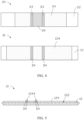
FIG. 3 is a top view of the negative electrode plate and the positive electrode plate shown inFIG. 2 ; -
FIG. 4 is a top view of a negative electrode plate and a positive electrode plate according to an embodiment of this application; -
FIG. 5 is a schematic sectional view of a negative electrode plate according to an embodiment of this application; -
FIG. 6 is a schematic sectional view of a negative electrode plate and a positive electrode plate according to an embodiment of this application. -
FIG. 7 is a schematic sectional view of a negative electrode plate and a positive electrode plate according to an embodiment of this application. -
FIG. 8 is a schematic sectional view of a negative electrode plate according to an embodiment of this application; -
FIG. 9 is a schematic sectional view of a negative electrode plate according to an embodiment of this application; -
FIG. 10 is a schematic sectional view of a positive electrode plate according to an embodiment of this application; -
FIG. 11 is a schematic sectional view of a positive electrode plate according to an embodiment of this application; and -
FIG. 12 is an schematic structural diagram of an electronic device according to an embodiment of this application. - Reference numerals of main components:
Electrochemical device 100 Negative electrode plate 10 Negative current collector 12 First surface 122 Negative active material layer 124 Superficial layer 1244 Groove 125 Negative tab 126 Second insulation layer 128 Positive electrode plate 20 Positive current collector 22 Second surface 222 Positive active material layer 24 First insulation layer 26 Separator 30 First region D1 Second region D2 Third region D3 Fourth region D4 Electronic device 200 - This application is further described below with reference to the following specific embodiments and the foregoing drawings.
- To make the foregoing objectives, features, and advantages of this application more comprehensible, the following describes this application in detail with reference to drawings and specific embodiments. It needs to be noted that to the extent that no conflict occurs, the embodiments of this application and the features in the embodiments may be combined with each other. For thorough understanding of this application, many details are given below. The embodiments described herein are merely a part of rather than all of the embodiments of this application. All other embodiments derived by a person of ordinary skill in the art based on the embodiments of the present invention fall within the protection scope of the present invention.
- Unless otherwise defined, all technical and scientific terms used herein have the same meanings as usually understood by a person skilled in the technical field of this application. The terms used in the specification of this application herein are merely intended for describing specific embodiments but are not intended to limit this application. The term "and/or" used herein includes any and all combinations of one or more related items preceding and following the term.
- As shown in
FIG. 1 , this application provides anelectrochemical device 100. Theelectrochemical device 100 includes any device capable of electrochemical reactions. Specifically, theelectrochemical device 100 includes all types of primary batteries, secondary batteries, and capacitors (such as supercapacitors). Optionally, theelectrochemical device 100 may be a lithium secondary battery, including a lithium metal secondary battery, a lithium-ion secondary battery, a lithium polymer secondary battery, and a lithium-ion polymer secondary battery. - In this embodiment, the
electrochemical device 100 includes anegative electrode plate 10, apositive electrode plate 20, and aseparator 30. Theseparator 30 is located between thenegative electrode plate 10 and thepositive electrode plate 20. Theelectrochemical device 100 further includes an electrolytic solution. The electrolytic solution infiltrates thenegative electrode plate 10, theseparator 30, and thepositive electrode plate 20. - As shown in
FIG. 2, FIG. 3 , andFIG. 4 , thenegative electrode plate 10 includes a negativecurrent collector 12. The negativecurrent collector 12 includes afirst surface 122. A negativeactive material layer 124 is disposed on thefirst surface 122. - The
positive electrode plate 20 includes a positivecurrent collector 22. The positivecurrent collector 22 includes asecond surface 222 facing towards thefirst surface 122. A positiveactive material layer 24 is disposed on thesecond surface 222. The positiveactive material layer 24 includes a first region D1. The first region D1 includes a second region D2 and a third region D3. The third region D3 is a region that does not overlap the second region D2 by any area in the first region D1. The negativeactive material layer 124 includes a fourth region D4 facing towards the third region D3. - The
first insulation layer 26 is disposed on the surface of the second region D2. Thefirst insulation layer 26 is disposed on a surface of the positiveactive material layer 24 facing opposite to the positivecurrent collector 22. Thefirst insulation layer 26 may overlap one edge of thenegative electrode plate 10 along a width direction of the negative electrode plate 10 (as shown inFIG. 3 ), or may overlap two opposite edges of thenegative electrode plate 10 along the width direction of the negative electrode plate 10 (as shown inFIG. 4 ), without being limited herein. - The
first insulation layer 26 may possess adhesive properties. Thefirst insulation layer 26 may be single-sided tape, double-sided tape, or hot-melt adhesive. Preferably, thefirst insulation layer 26 is double-sided tape or hot-melt adhesive, both sides of which possess adhesive properties, and can closely bond the positiveactive material layer 24 to theseparator 30 to improve the interface consistency of theelectrochemical device 100. - The area of the first region D1 is defined as S1 (mm2), and the area of the second region D2 is defined as S2 (mm2). The area S1 of the first region D1 and the area S2 of the second region D2 satisfy a relation: S2 < S1 ≤ 1.5S2. A ratio (Cell Balance, CB for short) of a unit-area capacity of the fourth region D4 to a unit-area capacity of the third region D3 is greater than or equal to 1.1.
- In order to prevent the
electrochemical device 100 from short-circuiting, afirst insulation layer 26 is disposed on the surface of the positiveactive material layer 24 in the second region D2. In this way, in a charge-and-discharge process of theelectrochemical device 100, lithium ions are still deintercalated from the positive active material located at the edge of the second region D2 and overlaid by thefirst insulation layer 26. The lithium ions are precipitated on the surface of the fourth region D4. The precipitated lithium metal pierces theseparator 30 to cause a short circuit of theelectrochemical device 100, thereby impairing safety and reliability. - In this application, by controlling the ratio of the unit-area capacity of the fourth region D4 to the unit-area capacity of the third region D3 to fall within a specified range, the ratio of the quantity of lithium ions that can be intercalated into the fourth region D4 to the quantity of lithium ions that can be deintercalated from the third region D3 falls within a specified range, thereby alleviating the problem of lithium plating on the surface of the negative
active material layer 124 and improving safety and reliability of theelectrochemical device 100. - In an embodiment of this application, the unit-area capacity of the fourth region D4 is greater than a unit-area capacity of a region of the negative
active material layer 124 different from the fourth region D4. The region of the negativeactive material layer 124 different from the fourth region D4 may a region coated with a normal negative active material, thereby increasing the unit-area capacity of the fourth region D4. This increases the ratio of the unit-area capacity of the fourth region D4 to the unit-area capacity of the third region D3, reduces risks of lithium plating on the surface of the negativeactive material layer 124 and improves safety and reliability. - As shown in
FIG. 5 , in an embodiment of this application, the region of the negativeactive material layer 124 different from the fourth region D4 includes a first negative active material. Asuperficial layer 1244 of the fourth region D4 includes a second negative active material. A gram capacity of the second negative active material is greater than a gram capacity of the first negative active material. The first negative active material is an active material that is normally coated on thenegative electrode plate 10. By setting at least a part of the active material in the fourth region D4 to possess a relatively high gram capacity, this embodiment can increase the quantity of lithium ions that can be intercalated into the fourth region D4, reduce risks of lithium plating on the surface of the negativeactive material layer 124, and improve safety and reliability. - Understandably, the negative
active material layer 124 located in the fourth region D4 may include a first negative active material, or may include no first negative active material. To be specific, the thickness of thesuperficial layer 1244 of the fourth region D4 can be increased by reducing the thickness of the first negative active material located in the fourth region D4, thereby increasing the quantity of lithium ions that can be intercalated into the fourth region D4, reducing risks of lithium plating on the surface of the negativeactive material layer 124, and improving safety and reliability. - In this application, the
superficial layer 1244 of the fourth region D4 is a superficial layer of the negativeactive material layer 124 in the fourth region D4. In an embodiment, the fourth region D4 is coated with a layer of negative active material, and then further coated with a layer of negative active material to form thesuperficial layer 1244. In an embodiment, the fourth region D4 is coated with a layer of negative active material, and then a side that is of the fourth region facing opposite to the negativecurrent collector 12 contains a negative active material of a specified thickness, known as thesuperficial layer 1244. Understandably, the formation manner of thesuperficial layer 1244 is not limited to the example above. - In an embodiment of this application, a lithiation potential versus Li/Li+ of the second negative active material is 0.2 V to 3.0 V This not only avoids further lithium plating on the second negative active material caused by a deficient lithiation potential (less than 0.2 V) of the second negative active material, but also avoids an excessive lithiation potential (higher than 3.0 V) of the second negative active material. The excessive lithiation potential has to be matched by a positive active material of a higher potential.
- In an embodiment of this application, the second negative active material is an active material in which lithium ions can be intercalated. The second negative active material includes, but is not limited to, metal oxide, carbon material, inorganic non-metallic simple substance, silicon-containing compound, or lithium salt. The metal oxide includes transition metal oxide, and the like. The carbon material includes graphene, hard carbon, soft carbon, artificial graphite, natural graphite, mesocarbon microbead, or the like. The inorganic non-metallic simple substance includes silicon, phosphorus, sulfur, or the like. The silicon-containing compound includes silicon-oxygen compound, silicon carbon compound, or the like. The lithium salt includes lithium titanium oxide, or the like. In this way, the second negative active material can have a relatively high gram capacity.
- In an embodiment of this application, a thickness of the
superficial layer 1244 of the fourth region D4 is less than or equal to 50 µm. By controlling the thickness of thesuperficial layer 1244 of the fourth region D4, on the one hand, this embodiment controls the thickness of theelectrochemical device 100 to be not excessive, and on the other hand, reduces cost on the basis of reducing risks of lithium plating. - In an embodiment of this application, the thickness of the
superficial layer 1244 of the fourth region D4 is 1 µm to 50 µm. - In an embodiment of this application, the thickness of the
superficial layer 1244 of the fourth region D4 is 1 µm to 25 µm. - In an embodiment of this application, the thickness of the
superficial layer 1244 of the fourth region D4 is 3 µm to 10 µm. - As shown in
FIG. 6 , in an embodiment of this application, agroove 125 is provided in a negativeactive material layer 124. Anegative tab 126 is accommodated in thegroove 125. Thenegative tab 126 is electrically connected to the negativecurrent collector 12. A projection of thegroove 125 on the positiveactive material layer 24 is located in the second region D2. - Understandably, the manner of electrical connection between the
negative tab 126 and the negativecurrent collector 12 may be, but without being limited to, welding, bonding, or the like, where the welding may be, but without being limited to, resistance welding, ultrasonic welding, laser welding, or the like. Thegroove 125 may be arranged in the following way: after thefirst surface 122 of the negativecurrent collector 12 is coated with the negativeactive material layer 124, the negativeactive material layer 124 is washed off a position where thenegative tabs 126 is located. The washing manner includes, but is not limited to, laser cleaning, or washing by using styrofoam, or the like. - After the
negative electrode plate 10, theseparator 30, and thepositive electrode plate 20 form theelectrochemical device 100, the negativeactive material layer 124 and the positiveactive material layer 24 are interspaced with, and fit closely with, theseparator 30. The second region D2 completely overlays thegroove 125. - As shown in
FIG. 7 , the second region D2 may at least just overlay thegroove 125. That is, the area of the second region D2 may be equal to the area of thegroove 125, and the second region D2 just overlays thegroove 125. The area of the second region D2 may be larger than the area of thegroove 125 instead. The width of thegroove 125 is 3 mm to 100 mm along a width direction of thenegative electrode plate 10. The length of thegroove 125 is 3 mm to 100 mm along a direction perpendicular to the width direction of thenegative electrode plate 10. The length and width of thegroove 125 are selected as required by the process. - Further, the projection of the
first insulation layer 26 on the negativeactive material layer 124 at least completely overlays thegroove 125. In this way, in a charge-and-discharge process of theelectrochemical device 100, a delithiation reaction of the active material of the second region D2 is hindered by thefirst insulation layer 26, and the quantity of lithium ions deintercalated will be greatly reduced. - As shown in
FIG. 8 , in an embodiment of this application, asecond insulation layer 128 is disposed on a surface of thenegative tab 126. A distance between a surface that is of asuperficial layer 1244 of the fourth region D4 facing opposite to the negativecurrent collector 12 and the negativecurrent collector 12 is less than or equal to a distance between a surface that is of thesecond insulation layer 128 facing opposite to the negativecurrent collector 12 and the negativecurrent collector 12. Further, thesecond insulation layer 128 may at least completely overlays thegroove 125. - The
negative tab 126 undergoes processes such as cutting during manufacture, and metal burrs are generated at the edge of the tab. Weld marks and the like are generated when thenegative tab 126 is joined (for example, welded) to the negativecurrent collector 12. Thesecond insulation layer 128 disposed on the surface of thenegative tab 126 can prevent burrs or weld marks from piercing theseparator 30, reduce risks of short circuits of theelectrochemical device 100, and improve safety and reliability. In addition, the thickness of thesuperficial layer 1244 of the fourth region D4 is set to be not greater than the thickness of thesecond insulation layer 128, so that the total thickness of theelectrochemical device 100 can be controlled not to be excessively thick. - The
second insulation layer 128 may possess adhesive properties. Thesecond insulation layer 128 may be single-sided tape, double-sided tape, hot-melt adhesive, or the like. Preferably, thesecond insulation layer 128 is double-sided tape or hot-melt adhesive, both sides of which possess adhesive properties, and can closely bond the negativeactive material layer 124 to theseparator 30 to improve the interface consistency of theelectrochemical device 100. - In an embodiment of this application, the surface of the
negative tab 126 is overlaid with the negative active material. On the one hand, this increases the amount of active material of theelectrochemical device 100 and increases the energy density. In addition, the negative active material layer that overlays the surface of thenegative tab 126 can cover the burrs or weld marks generated in cutting and joining (such as welding) of thenegative tab 126, avoid a short circuit caused by piercing of theseparator 30, and improve safety and reliability. Further, as shown inFIG. 9 , the region located in the negativeactive material layer 124 and corresponding to the second region D2 is fully overlaid with the negative active material, and is overlaid with the same second negative active material as thesuperficial layer 1244 of the fourth region D4. Further, the negativeactive material layer 124 can fill thegroove 125. - In an embodiment of this application, the third region includes a first positive active material. A region of the positive
active material layer 24 different from the third region D3 includes a second positive active material. The unit-area capacity of the third region D3 is less than a unit-area capacity of the region of the positiveactive material layer 24 different from the third region D3. By reducing the unit-area capacity of the third region D3, the quantity of lithium ions that can be deintercalated from the third region D3 is less than that in a normal circumstance, thereby increasing the ratio of the unit-area capacity of the fourth region D4 to the unit-area capacity of the third region D3, avoiding lithium plating on the surface of the negativeactive material layer 124, and improving safety and reliability. - In an embodiment of this application, a gram capacity of the first positive active material is less than a gram capacity of the second positive active material. To be specific, by coating the third region D3 with a positive active material of a relatively low gram capacity, the quantity of lithium ions that can be deintercalated from the first positive active material of the third region D3 is reduced, so as to further avoid lithium plating on the surface of the negative
active material layer 124 and improve safety and reliability. - Table 1 enumerates some positive active materials and their gram capacities. The corresponding first positive active material and second positive active material may be selected based on the gram capacities of the positive active materials, and applied to corresponding regions. In the embodiments of this application, one of the following positive active materials may be selected as the first positive active material or the second positive active material. Alternatively, a mixture of two or more selected from the following positive active materials may be applied to the corresponding regions. However, understandably, Table 1 merely enumerates some of the positive active materials as examples, and the implementation of this application is not limited to the enumerated positive active materials. In addition, the gram capacity set out in Table 1 is the gram capacity actually achievable by the positive active material. Modification of the positive active material will change the gram capacity to some extent.
Table 1 Molecular formula of positive active material Abbreviation Gram capacity (mAh/g) Average voltage (vs Li/Li+) LiCoO2-140 LCO-140 140 3.8 LiCoO2-180 LCO-180 180 4.3 LiCoO2-220 LCO-220 220 4.3 LiMn2O4 LMO 130 4.05 LiFePO4 LFP 160 3.4 LiCoPO4 LCP 130 4.8 LiNiO2 LNO 200 3.7 LiNi0.33Mn0.33Co0.33O2 NCM333 160 3.7 LiNi0.5Mn0.2Co0.3O2 NCM523 180 3.7 LiNi0.6Mn0.2Co0.2O2 NCM622 200 3.7 LiNi0.8Mn0.1Co0.1O2 NCM811 220 3.7 xLi2MnO3(1-x)LiMO2(M=Ni,Co, Mn)-250 Li-rich-250 250 3.75 xLi2MnO3(1-x)LiMO2(M=Ni,Co, Mn)-280 Li-rich-280 280 3.75 xLi2MnO3(1-x)LiMO2(M=Ni,Co, Mn)-300 Li-rich-300 300 3.75 LiNi0.8Co0.15Al0.05O2-180 NCA-180 180 3.7 LiNi0.8Co0.15Al0.05O2-200 NCA-200 200 3.7 LiNi0.8Co0.15Al0.05O2-220 NCA-220 220 3.7 LiNi0.5Mn1.5O4 LNM 135 4.7 Li3V2(PO4)3 LVP 180 3.8 - As shown in
FIG. 10 , in an embodiment of this application, the thickness of the positiveactive material layer 24 located in the third region D3 is less than the thickness of the positiveactive material layer 24 in a region of the positiveactive material layer 24 different from the third region D3. With the decrease of the thickness of the positiveactive material layer 24 in the third region D3, the lithium ions that can be deintercalated from the third region are reduced, thereby further avoiding lithium plating on the surface of thenegative electrode plate 10 and improving safety and reliability. - As shown in
FIG. 11 , in an embodiment of this application, the third region D3 is provided without the positiveactive material layer 24. That is, the thickness of the positiveactive material layer 24 of the third region D3 is reduced to zero. The third region D3 is not coated with the positive active material, thereby avoiding lithium plating on the surface of the negativeactive material layer 124 and improving safety and reliability. - This application further provides an
electronic device 200. Theelectronic device 200 includes theelectrochemical device 100. Theelectronic device 200 may be a consumer electronic products (such as a mobile communication device, a tablet computer, a notebook computer, or a wearable device), a power tool, an unmanned aerial vehicle, an energy storage device, a power device, or the like. Referring toFIG. 12 , in an embodiment, theelectronic device 200 is a mobile communication device. - The
electrochemical device 100 according to this application increases the unit-area capacity of the fourth region D4 on the one hand, and on the other hand, reduces the unit-area capacity of the third region D3, so that the ratio of the unit-area capacity of the fourth region D4 to the unit-area capacity of the third region D3 is greater than or equal to 1.1, thereby solving the problem of lithium plating on the corresponding negativeactive material layer 124 in the regions around thefirst insulation layer 26 to improve safety and reliability of theelectrochemical device 100. - The foregoing embodiments are merely intended for describing the technical solutions of this application but not intended as a limitation. Although this application is described in detail with reference to the foregoing optional embodiments, a person of ordinary skill in the art understands that modifications or equivalent substitutions may be made to the technical solutions of this application without departing from the spirit and scope of the technical solutions of this application.
Claims (15)
- An electrochemical device, comprising:a negative electrode plate comprising a negative current collector, wherein the negative current collector comprises a first surface, and a negative active material layer is disposed on the first surface; anda positive electrode plate comprising a positive current collector, wherein the positive current collector comprises a second surface facing towards the first surface, and a positive active material layer is disposed on the second surface; characterized in that,the positive active material layer comprises a first region, the first region comprises a second region and a third region, a first insulation layer is disposed on a surface of the second region, the third region is a region that does not overlap the second region by any area in the first region, and the negative active material layer comprises a fourth region facing towards the third region;wherein an area S2 (mm2) of the second region and an area S1 (mm2) of the first region satisfy a relation: S2 < S1 ≤ 1.5S2, and a ratio CB of a unit-area capacity of the fourth region to a unit-area capacity of the third region is greater than or equal to 1.1.
- The electrochemical device according to claim 1, wherein the unit-area capacity of the fourth region is greater than a unit-area capacity of a region of the negative active material layer different from the fourth region.
- The electrochemical device according to claim 2, characterized in that, the region of the negative active material layer different from the fourth region comprises a first negative active material, a superficial layer of the fourth region comprises a second negative active material, and a gram capacity of the second negative active material is greater than a gram capacity of the first negative active material.
- The electrochemical device according to claim 3, characterized in that, a lithiation potential versus Li/Li+ of the second negative active material is 0.2 V to 3.0 V
- The electrochemical device according to claim 3, characterized in that, the second negative active material comprises at least one of transition metal oxide, lithium titanium oxide, graphene, hard carbon, soft carbon, silicon, silicon-oxygen compound, silicon-carbon compound, artificial graphite, natural graphite, mesocarbon microbead, phosphorus, or sulfur.
- The electrochemical device according to claim 3, characterized in that, a thickness of the superficial layer of the fourth region is less than or equal to 50 µm.
- The electrochemical device according to claim 1, characterized in that, a groove is provided in the negative active material layer, a negative tab is accommodated in the groove, the negative tab is electrically connected to the negative current collector, and a projection of the groove on the positive active material layer is located in the second region.
- The electrochemical device according to claim 7, characterized in that, the area of the second region is equal to an area of the groove.
- The electrochemical device according to claim 7, characterized in that, a second insulation layer is disposed on a surface of the negative tab, and a distance between a surface of the superficial layer of the fourth region facing opposite to the negative current collector and the negative current collector is less than or equal to a distance between a surface of the second insulation layer facing opposite to the negative current collector and the negative current collector.
- The electrochemical device according to claim 7, characterized in that, a surface of the negative tab is overlaid with the negative active material layer.
- The electrochemical device according to claim 1, characterized in that, the third region comprises a first positive active material, a region of the positive active material layer different from the third region comprises a second positive active material, and the unit-area capacity of the third region is less than a unit-area capacity of the region of the positive active material layer different from the third region.
- The electrochemical device according to claim 11, characterized in that, a gram capacity of the first positive active material is less than a gram capacity of the second positive active material.
- The electrochemical device according to claim 11, characterized in that, a thickness of the third region is less than a thickness of the region of the positive active material layer different from the third region.
- The electrochemical device according to claim 13, characterized in that, the third region is provided without the positive active material layer (D4).
- An electronic device, comprising the electrochemical device according to any one of claims 1 to 14.
Applications Claiming Priority (1)
| Application Number | Priority Date | Filing Date | Title |
|---|---|---|---|
| PCT/CN2020/082250 WO2021195907A1 (en) | 2020-03-31 | 2020-03-31 | Electrochemical apparatus and electronic apparatus |
Publications (2)
| Publication Number | Publication Date |
|---|---|
| EP4131543A1 true EP4131543A1 (en) | 2023-02-08 |
| EP4131543A4 EP4131543A4 (en) | 2023-11-29 |
Family
ID=77927333
Family Applications (1)
| Application Number | Title | Priority Date | Filing Date |
|---|---|---|---|
| EP20929306.7A Pending EP4131543A4 (en) | 2020-03-31 | 2020-03-31 | Electrochemical apparatus and electronic apparatus |
Country Status (4)
| Country | Link |
|---|---|
| US (1) | US20230040107A1 (en) |
| EP (1) | EP4131543A4 (en) |
| CN (1) | CN113544876B (en) |
| WO (1) | WO2021195907A1 (en) |
Cited By (1)
| Publication number | Priority date | Publication date | Assignee | Title |
|---|---|---|---|---|
| EP4550441A4 (en) * | 2022-07-01 | 2025-08-13 | Ningde Amperex Technology Ltd | Electrochemical device and preparation method therefor, and electronic device |
Families Citing this family (13)
| Publication number | Priority date | Publication date | Assignee | Title |
|---|---|---|---|---|
| CN115380411A (en) * | 2021-11-12 | 2022-11-22 | 宁德新能源科技有限公司 | Electrochemical device and electronic device including the same |
| CN114068859B (en) * | 2021-11-18 | 2023-05-16 | 珠海冠宇电池股份有限公司 | Positive plate and battery |
| CN114188501B (en) * | 2021-11-23 | 2024-08-13 | 宁德新能源科技有限公司 | Electrochemical devices and electronic devices |
| CN114464769B (en) * | 2021-12-17 | 2024-08-06 | 宁德新能源科技有限公司 | Electrode assembly, electrochemical device, and electricity using device |
| CN115843394B (en) * | 2022-02-10 | 2025-03-25 | 宁德新能源科技有限公司 | Cells, batteries and electrical equipment |
| JP2025510921A (en) * | 2022-03-31 | 2025-04-15 | 寧徳新能源科技有限公司 | Electrochemical and Electronic Devices |
| CN114583289B (en) * | 2022-03-31 | 2024-07-23 | 珠海冠宇电池股份有限公司 | A lithium ion battery |
| CN118352745A (en) * | 2022-03-31 | 2024-07-16 | 东莞新能安科技有限公司 | Electrochemical devices and electronic devices |
| JP2025504446A (en) * | 2022-06-17 | 2025-02-12 | 珠海冠宇電池股分有限公司 | Plates and batteries |
| EP4528839A4 (en) * | 2022-06-21 | 2026-01-14 | Ningde Amperex Technology Ltd | ELECTROCHEMICAL DEVICE AND ELECTRICAL DEVICE |
| CN116072817B (en) * | 2023-03-31 | 2023-06-13 | 宁德新能源科技有限公司 | Electrochemical devices and electrical devices |
| WO2026000432A1 (en) * | 2024-06-28 | 2026-01-02 | 宁德时代新能源科技股份有限公司 | Battery cell, battery device, and electric device |
| CN119890411B (en) * | 2025-01-21 | 2025-11-07 | 深圳市豪鹏科技股份有限公司 | Lithium ion battery and preparation method thereof |
Family Cites Families (19)
| Publication number | Priority date | Publication date | Assignee | Title |
|---|---|---|---|---|
| KR100449757B1 (en) * | 2001-11-23 | 2004-09-22 | 삼성에스디아이 주식회사 | Battery unit and secondary battery applying the such |
| CN101286574A (en) * | 2008-05-21 | 2008-10-15 | 方祺 | Cylindrical lithium ion battery |
| JP5627250B2 (en) * | 2010-02-25 | 2014-11-19 | 日立オートモティブシステムズ株式会社 | Lithium ion battery |
| CN102306778B (en) * | 2011-09-02 | 2013-10-16 | 惠州市惠德瑞锂电科技有限公司 | Nonaqueous electrochemical battery and preparation method thereof |
| CN203521537U (en) * | 2013-10-17 | 2014-04-02 | 东莞新能源科技有限公司 | Laminated lithium ion battery cell |
| US10147556B2 (en) * | 2014-03-31 | 2018-12-04 | Semiconductor Energy Laboratory Co., Ltd. | Power storage device and electronic device |
| CN105514350A (en) * | 2014-09-25 | 2016-04-20 | 东莞新能源科技有限公司 | Lithium ion battery |
| CN105990610B (en) * | 2015-02-05 | 2018-07-10 | 东莞新能源科技有限公司 | Flexible battery cell |
| CN105449264B (en) * | 2015-03-24 | 2017-11-17 | 万向一二三股份公司 | A kind of high voltage cobalt acid lithium/lithium titanate battery and preparation method thereof |
| KR102484265B1 (en) * | 2015-12-22 | 2023-01-02 | 삼성에스디아이 주식회사 | Electrode assembly and secondary battery using for the same |
| CN108701552B (en) * | 2016-02-29 | 2020-08-04 | 松下知识产权经营株式会社 | Electrochemical device and negative electrode used therein, and method for producing the same |
| CN205992575U (en) * | 2016-07-21 | 2017-03-01 | 中航锂电(洛阳)有限公司 | Positive plate and coiled lithium-ion power battery core and lithium-ion-power cell |
| CN110752346B (en) * | 2018-07-23 | 2021-02-12 | 北京好风光储能技术有限公司 | Back-to-back deposition type metal cathode and back-to-back deposition type metal cathode battery |
| CN110660999A (en) * | 2018-09-30 | 2020-01-07 | 宁德时代新能源科技股份有限公司 | A current collector, pole piece and electrochemical device |
| CN208819985U (en) * | 2018-10-29 | 2019-05-03 | 宁德时代新能源科技股份有限公司 | Electrode, electrode assembly and secondary battery |
| CN110660963B (en) * | 2018-12-29 | 2021-04-27 | 宁德时代新能源科技股份有限公司 | An electrode pole piece and electrochemical device |
| CN109817884A (en) * | 2018-12-29 | 2019-05-28 | 深圳市卓能新能源股份有限公司 | Battery anode slice and preparation method thereof and lithium ion battery |
| KR102086783B1 (en) * | 2019-03-27 | 2020-03-09 | 광주과학기술원 | Thick film electrode for lithium secondary battery and lithium secondary battery |
| CN112133925B (en) * | 2019-04-26 | 2021-10-26 | 宁德时代新能源科技股份有限公司 | Battery, electric automobile and consumer electronics |
-
2020
- 2020-03-31 EP EP20929306.7A patent/EP4131543A4/en active Pending
- 2020-03-31 WO PCT/CN2020/082250 patent/WO2021195907A1/en not_active Ceased
- 2020-03-31 CN CN202080008267.9A patent/CN113544876B/en active Active
-
2022
- 2022-09-29 US US17/956,272 patent/US20230040107A1/en active Pending
Cited By (1)
| Publication number | Priority date | Publication date | Assignee | Title |
|---|---|---|---|---|
| EP4550441A4 (en) * | 2022-07-01 | 2025-08-13 | Ningde Amperex Technology Ltd | Electrochemical device and preparation method therefor, and electronic device |
Also Published As
| Publication number | Publication date |
|---|---|
| WO2021195907A1 (en) | 2021-10-07 |
| US20230040107A1 (en) | 2023-02-09 |
| CN113544876A (en) | 2021-10-22 |
| EP4131543A4 (en) | 2023-11-29 |
| CN113544876B (en) | 2024-07-05 |
Similar Documents
| Publication | Publication Date | Title |
|---|---|---|
| US20230040107A1 (en) | Electrochemical device and electronic device | |
| EP4089760B1 (en) | Electrochemical device and electronic device | |
| JP6676399B2 (en) | Bipolar lithium-ion battery and method of manufacturing bipolar lithium-ion battery | |
| EP4297119A1 (en) | Electrochemical device and electronic device | |
| TWI343668B (en) | Electrode for lithium secondary battery comprising electrode additive and lithium secondary battery using the same | |
| US20040137326A1 (en) | Lithium ion battery and methods of manufacturing same | |
| KR102739840B1 (en) | LITHIUM SECONDARY BATTERY COMPRISING Si-BASED COMPOUND WITH EXCELLENT ENERGY DENSITY | |
| CN102148357B (en) | For the negative pole of lithium rechargeable battery, lithium rechargeable battery, electric power tool, motor vehicle and power storage system | |
| KR20150108825A (en) | Secondary battery, secondary battery module, method for charging the secondary battery and the secondary battery module, method for discharging the secondary battery and the secondary battery module, method for operating the secondary battery and the secondary battery module, power storage system, and method for operating the power storage system | |
| CN115191047B (en) | Collector, power storage element, and power storage module | |
| WO2022057189A1 (en) | Solid-state battery, battery module, battery pack, and related device thereof | |
| US12548759B2 (en) | Battery and method for producing same | |
| EP4246625A1 (en) | Electrochemical apparatus and electronic apparatus | |
| US12355036B2 (en) | All-solid-state rechargeable battery and stacked all-solid-state rechargeable battery | |
| CN205723642U (en) | Battery cell, battery pack and device including battery pack | |
| CN116072817A (en) | Electrochemical devices and electrical devices | |
| JP2007048662A (en) | Auxiliary power supply | |
| KR20150070939A (en) | Secondary battery and preparation method thereof | |
| JP7246196B2 (en) | All-solid lithium secondary battery | |
| EP4362214A1 (en) | Electrochemical device and electronic device | |
| JP7196720B2 (en) | laminated battery | |
| EP3859859A1 (en) | Electrolyte for lithium ion secondary battery and lithium ion secondary battery | |
| EP4362213A1 (en) | Electrochemical device and electronic device | |
| KR102733613B1 (en) | all solid state rechargeable battery and stacked all solid state rechargeable battery | |
| KR102795173B1 (en) | Electrode plate for lithium secondary battery and method of manufacturing the same |
Legal Events
| Date | Code | Title | Description |
|---|---|---|---|
| STAA | Information on the status of an ep patent application or granted ep patent |
Free format text: STATUS: THE INTERNATIONAL PUBLICATION HAS BEEN MADE |
|
| PUAI | Public reference made under article 153(3) epc to a published international application that has entered the european phase |
Free format text: ORIGINAL CODE: 0009012 |
|
| STAA | Information on the status of an ep patent application or granted ep patent |
Free format text: STATUS: REQUEST FOR EXAMINATION WAS MADE |
|
| 17P | Request for examination filed |
Effective date: 20221028 |
|
| AK | Designated contracting states |
Kind code of ref document: A1 Designated state(s): AL AT BE BG CH CY CZ DE DK EE ES FI FR GB GR HR HU IE IS IT LI LT LU LV MC MK MT NL NO PL PT RO RS SE SI SK SM TR |
|
| DAV | Request for validation of the european patent (deleted) | ||
| DAX | Request for extension of the european patent (deleted) | ||
| A4 | Supplementary search report drawn up and despatched |
Effective date: 20231031 |
|
| RIC1 | Information provided on ipc code assigned before grant |
Ipc: H01M 50/531 20210101ALI20231025BHEP Ipc: H01M 4/36 20060101ALI20231025BHEP Ipc: H01M 4/13 20100101ALI20231025BHEP Ipc: H01M 4/66 20060101ALI20231025BHEP Ipc: H01M 4/139 20100101ALI20231025BHEP Ipc: H01M 10/0525 20100101AFI20231025BHEP |