EP4131508A1 - Pole piece, cell and battery - Google Patents
Pole piece, cell and battery Download PDFInfo
- Publication number
- EP4131508A1 EP4131508A1 EP20927603.9A EP20927603A EP4131508A1 EP 4131508 A1 EP4131508 A1 EP 4131508A1 EP 20927603 A EP20927603 A EP 20927603A EP 4131508 A1 EP4131508 A1 EP 4131508A1
- Authority
- EP
- European Patent Office
- Prior art keywords
- conductive layer
- electrode plate
- layer
- edge region
- conductive
- Prior art date
- Legal status (The legal status is an assumption and is not a legal conclusion. Google has not performed a legal analysis and makes no representation as to the accuracy of the status listed.)
- Pending
Links
- 229920000642 polymer Polymers 0.000 claims abstract description 17
- 238000009413 insulation Methods 0.000 claims description 41
- 239000011149 active material Substances 0.000 claims description 37
- 239000006258 conductive agent Substances 0.000 claims description 11
- 239000011230 binding agent Substances 0.000 claims description 9
- 229920000178 Acrylic resin Polymers 0.000 description 19
- 239000004925 Acrylic resin Substances 0.000 description 19
- OKTJSMMVPCPJKN-UHFFFAOYSA-N Carbon Chemical compound [C] OKTJSMMVPCPJKN-UHFFFAOYSA-N 0.000 description 19
- 239000002041 carbon nanotube Substances 0.000 description 17
- 229910021393 carbon nanotube Inorganic materials 0.000 description 17
- 230000000052 comparative effect Effects 0.000 description 16
- 239000002002 slurry Substances 0.000 description 11
- HBBGRARXTFLTSG-UHFFFAOYSA-N Lithium ion Chemical compound [Li+] HBBGRARXTFLTSG-UHFFFAOYSA-N 0.000 description 7
- 229910001416 lithium ion Inorganic materials 0.000 description 7
- 238000002156 mixing Methods 0.000 description 7
- 239000000843 powder Substances 0.000 description 7
- 239000002070 nanowire Substances 0.000 description 6
- 239000011248 coating agent Substances 0.000 description 5
- 238000000576 coating method Methods 0.000 description 5
- 238000007599 discharging Methods 0.000 description 5
- 229910052751 metal Inorganic materials 0.000 description 5
- 239000002184 metal Substances 0.000 description 5
- RYGMFSIKBFXOCR-UHFFFAOYSA-N Copper Chemical compound [Cu] RYGMFSIKBFXOCR-UHFFFAOYSA-N 0.000 description 4
- SECXISVLQFMRJM-UHFFFAOYSA-N N-Methylpyrrolidone Chemical compound CN1CCCC1=O SECXISVLQFMRJM-UHFFFAOYSA-N 0.000 description 4
- 239000002033 PVDF binder Substances 0.000 description 3
- 239000002131 composite material Substances 0.000 description 3
- 229910052802 copper Inorganic materials 0.000 description 3
- 239000010949 copper Substances 0.000 description 3
- 239000011888 foil Substances 0.000 description 3
- 229920002981 polyvinylidene fluoride Polymers 0.000 description 3
- 238000002360 preparation method Methods 0.000 description 3
- 238000005524 ceramic coating Methods 0.000 description 2
- 230000007423 decrease Effects 0.000 description 2
- 238000010586 diagram Methods 0.000 description 2
- 239000003292 glue Substances 0.000 description 2
- 238000004519 manufacturing process Methods 0.000 description 2
- 239000000463 material Substances 0.000 description 2
- 239000000203 mixture Substances 0.000 description 2
- 239000002904 solvent Substances 0.000 description 2
- 238000003756 stirring Methods 0.000 description 2
- 229920000049 Carbon (fiber) Polymers 0.000 description 1
- BQCADISMDOOEFD-UHFFFAOYSA-N Silver Chemical compound [Ag] BQCADISMDOOEFD-UHFFFAOYSA-N 0.000 description 1
- 239000002042 Silver nanowire Substances 0.000 description 1
- 229920002125 Sokalan® Polymers 0.000 description 1
- 239000006230 acetylene black Substances 0.000 description 1
- 239000013543 active substance Substances 0.000 description 1
- 229910052782 aluminium Inorganic materials 0.000 description 1
- XAGFODPZIPBFFR-UHFFFAOYSA-N aluminium Chemical compound [Al] XAGFODPZIPBFFR-UHFFFAOYSA-N 0.000 description 1
- 239000006229 carbon black Substances 0.000 description 1
- 239000004917 carbon fiber Substances 0.000 description 1
- 239000011889 copper foil Substances 0.000 description 1
- 230000003247 decreasing effect Effects 0.000 description 1
- 239000010439 graphite Substances 0.000 description 1
- 229910002804 graphite Inorganic materials 0.000 description 1
- 238000010030 laminating Methods 0.000 description 1
- 239000002923 metal particle Substances 0.000 description 1
- 238000000034 method Methods 0.000 description 1
- 238000012986 modification Methods 0.000 description 1
- 230000004048 modification Effects 0.000 description 1
- 239000002245 particle Substances 0.000 description 1
- 229920000058 polyacrylate Polymers 0.000 description 1
- 239000004584 polyacrylic acid Substances 0.000 description 1
- 229920002239 polyacrylonitrile Polymers 0.000 description 1
- 229920002635 polyurethane Polymers 0.000 description 1
- 239000004814 polyurethane Substances 0.000 description 1
- 238000004804 winding Methods 0.000 description 1
Images





Classifications
-
- H—ELECTRICITY
- H01—ELECTRIC ELEMENTS
- H01M—PROCESSES OR MEANS, e.g. BATTERIES, FOR THE DIRECT CONVERSION OF CHEMICAL ENERGY INTO ELECTRICAL ENERGY
- H01M4/00—Electrodes
- H01M4/02—Electrodes composed of, or comprising, active material
- H01M4/64—Carriers or collectors
- H01M4/66—Selection of materials
- H01M4/665—Composites
- H01M4/667—Composites in the form of layers, e.g. coatings
-
- H—ELECTRICITY
- H01—ELECTRIC ELEMENTS
- H01M—PROCESSES OR MEANS, e.g. BATTERIES, FOR THE DIRECT CONVERSION OF CHEMICAL ENERGY INTO ELECTRICAL ENERGY
- H01M10/00—Secondary cells; Manufacture thereof
- H01M10/05—Accumulators with non-aqueous electrolyte
- H01M10/052—Li-accumulators
- H01M10/0525—Rocking-chair batteries, i.e. batteries with lithium insertion or intercalation in both electrodes; Lithium-ion batteries
-
- H—ELECTRICITY
- H01—ELECTRIC ELEMENTS
- H01M—PROCESSES OR MEANS, e.g. BATTERIES, FOR THE DIRECT CONVERSION OF CHEMICAL ENERGY INTO ELECTRICAL ENERGY
- H01M10/00—Secondary cells; Manufacture thereof
- H01M10/42—Methods or arrangements for servicing or maintenance of secondary cells or secondary half-cells
- H01M10/4235—Safety or regulating additives or arrangements in electrodes, separators or electrolyte
-
- H—ELECTRICITY
- H01—ELECTRIC ELEMENTS
- H01M—PROCESSES OR MEANS, e.g. BATTERIES, FOR THE DIRECT CONVERSION OF CHEMICAL ENERGY INTO ELECTRICAL ENERGY
- H01M10/00—Secondary cells; Manufacture thereof
- H01M10/60—Heating or cooling; Temperature control
- H01M10/61—Types of temperature control
- H01M10/613—Cooling or keeping cold
-
- H—ELECTRICITY
- H01—ELECTRIC ELEMENTS
- H01M—PROCESSES OR MEANS, e.g. BATTERIES, FOR THE DIRECT CONVERSION OF CHEMICAL ENERGY INTO ELECTRICAL ENERGY
- H01M4/00—Electrodes
- H01M4/02—Electrodes composed of, or comprising, active material
- H01M4/13—Electrodes for accumulators with non-aqueous electrolyte, e.g. for lithium-accumulators; Processes of manufacture thereof
-
- H—ELECTRICITY
- H01—ELECTRIC ELEMENTS
- H01M—PROCESSES OR MEANS, e.g. BATTERIES, FOR THE DIRECT CONVERSION OF CHEMICAL ENERGY INTO ELECTRICAL ENERGY
- H01M4/00—Electrodes
- H01M4/02—Electrodes composed of, or comprising, active material
- H01M4/64—Carriers or collectors
- H01M4/66—Selection of materials
- H01M4/668—Composites of electroconductive material and synthetic resins
-
- Y—GENERAL TAGGING OF NEW TECHNOLOGICAL DEVELOPMENTS; GENERAL TAGGING OF CROSS-SECTIONAL TECHNOLOGIES SPANNING OVER SEVERAL SECTIONS OF THE IPC; TECHNICAL SUBJECTS COVERED BY FORMER USPC CROSS-REFERENCE ART COLLECTIONS [XRACs] AND DIGESTS
- Y02—TECHNOLOGIES OR APPLICATIONS FOR MITIGATION OR ADAPTATION AGAINST CLIMATE CHANGE
- Y02E—REDUCTION OF GREENHOUSE GAS [GHG] EMISSIONS, RELATED TO ENERGY GENERATION, TRANSMISSION OR DISTRIBUTION
- Y02E60/00—Enabling technologies; Technologies with a potential or indirect contribution to GHG emissions mitigation
- Y02E60/10—Energy storage using batteries
Definitions
- This application relates to the field of batteries, and in particular, to an electrode plate, a cell containing such electrode plate, and a battery containing such cell.
- lithium-ion batteries being widely applied in fields such as electric tools, electric vehicles, and portable devices, scenarios where lithium-ion batteries are used have become increasingly complex, making safety requirements for lithium-ion batteries more rigorous.
- metal foils such as copper foils and aluminum foils are used as current collectors of lithium-ion batteries.
- composite current collectors are usually used to replace conventional metal foils in lithium-ion batteries.
- surface resistance of a composite current collector is about 100 times that of a conventional current collector with same thickness, this leads to too much temperature rise in high power density batteries during charging and discharging, which is unable to satisfy requirements of actual application scenarios and causes huge potential safety hazards.
- the embodiments of this application provide an electrode plate including a current collector.
- the current collector includes a macromolecular polymer layer and a first conductive layer.
- the first conductive layer is disposed on a surface of the macromolecular polymer layer.
- a second conductive layer is provided on a surface of the first conductive layer in an edge region in a widthwise direction of the electrode plate.
- the second conductive layer extends in a lengthwise direction of the electrode plate, and the first conductive layer is disposed between the second conductive layer and the macromolecular polymer layer.
- an insulation layer is provided on a surface of the second conductive layer, and the second conductive layer is disposed between the first conductive layer and the insulation layer.
- an active material layer is provided on a surface of the first conductive layer, and the active material layer connects with the second conductive layer and the insulation layer.
- the edge region in the widthwise direction of the electrode plate, includes a first edge region and a second edge region opposite the first edge region, and the second conductive layer extends from the first edge region to the second edge region of the electrode plate.
- an active material layer is provided on a surface of the second conductive layer and an insulation layer is provided on a surface of the second conductive layer in the first edge region or the second edge region of the electrode plate.
- the active material layer connects with the insulation layer.
- a gap is present between the active material layer and the insulation layer.
- the second conductive layer includes a conductive agent and a binder, where a proportion of the conductive agent is 1%-80% and a proportion of the binder is 2%-60%.
- surface resistance of the second conductive layer is less than 1 ⁇ /cm 2 .
- adhesion between the second conductive layer and the current collector is greater than or equal to 10 N/m
- thickness of the second conductive layer is 10 ⁇ m-100 ⁇ m, and thickness of the insulation layer is less than 20 ⁇ m.
- An embodiment of this application further provides a cell, including an electrode assembly.
- the electrode assembly includes any one of the foregoing electrode plates.
- An embodiment of this application further provides a battery including the foregoing cells and a housing configured to accommodate the cell.
- the second conductive layer is disposed on the edge region or the entire surface of the first conductive layer in the widthwise direction of the electrode plate, so that the second conductive layer and the current collector form a parallel structure, thereby effectively reducing resistance of the electrode plate, which in turn decreases heat production and temperature rise of the cell and battery during charging and discharging, improving reliability of the cell and the battery in use.
- the second conductive layer being disposed on the edge region or the entire surface of the first conductive layer in the widthwise direction of the electrode plate also allows electrons generated by the active material layer during charging and discharging to move to the second conductive layer through the first conductive layer, which are then transferred rapidly along the lengthwise direction of the electrode plate. This reduces resistance to the transverse transport of electrons, improving transverse electron transport capacity of the electrode plate, and thus effectively reducing internal resistance of the cell and improving safety performance of the battery in use.
- an embodiment of this application provides an electrode plate 100.
- the electrode plate 100 includes a current collector 11.
- the current collector 11 includes a macromolecular polymer layer 111 and a first conductive layer 112
- the first conductive layer 112 is disposed on a surface of the macromolecular polymer layer 111.
- the electrode plate 100 further includes a second conductive layer 12.
- the second conductive layer 12 is provided on a surface of the first conductive layer 112 in an edge region 1001 in a widthwise direction (that is, an X-axis direction) of the electrode plate 100 (see FIG. 1 and FIG. 4 ).
- the second conductive layer 12 extends in a lengthwise direction (that is, a Y-axis direction) of the electrode plate 100, and the first conductive layer 112 is disposed between the second conductive layer 12 and the macromolecular polymer layer 111. In this way, the second conductive layer 12 and the current collector 11 form a parallel structure, thereby effectively reducing resistance of the electrode plate 100.
- the electrode plate 100 further includes an insulation layer 13 provided on a surface of the second conductive layer 12.
- the second conductive layer 12 is disposed between the first conductive layer 112 and the insulation layer 13.
- an active material layer 14 is provided on a surface of the first conductive layer 112.
- the active material layer 14 connects with the second conductive layer 12 and the insulation layer 13.
- the active material layer 14 only connects with the second conductive layer 12; or a gap is present between the active material layer 14 and the second conductive layer 12 or between the active material layer 14 and the insulation layer 13.
- the edge region 1001 in the widthwise direction of the electrode plate 100, includes a first edge region 1002 and a second edge region 1003 opposite the first edge region 1002.
- the second conductive layer 12 extends from the first edge region 1002 to the second edge region 1003 of the electrode plate 100.
- the active material layer 14 is provided on a surface of the second conductive layer 12.
- the insulation layer 13 is provided on a surface of the second conductive layer 12 in the first edge region 1002 or the second edge region 1003 of the electrode plate 100.
- the active material layer 14 connects with the insulation layer 13.
- a gap is present between the active material layer 14 and the insulation layer 13.
- the second conductive layer 12 includes a conductive agent and a binder.
- a proportion of the conductive agent is 1%-80% and a proportion of the binder is 2%-60%. In this way, both good adhesion performance between the second conductive layer 12 and the current collector 11 and good conductive performance of the second conductive layer 12 are ensured.
- the conductive agent includes one or more of carbon black particles, carbon nanotubes, graphite flakes, carbon fibers, acetylene black, metal particles, and metal nanowire.
- the conductive agent includes metal nanowire.
- the metal nanowire is not limited to copper nanowire, silver nanowire, or the like.
- the binder may be polyvinylidene fluoride, polyacrylic acid, polyacrylate, polyacrylonitrile, polyurethane, acrylic resin, or modified materials thereof.
- the binder is acrylic resin.
- surface resistance of the second conductive layer 12 is less than 1 ⁇ /cm 2 . In an implementation, surface resistance of the second conductive layer 12 is less than or equal to 0.01 ⁇ /cm 2 .
- adhesion between the second conductive layer 12 and the current collector 11 is greater than or equal to 10 N/m. In an implementation, adhesion between the second conductive layer 12 and the current collector 11 is greater than or equal to 50 N/m.
- thickness T1 of the second conductive layer 12 is 10 ⁇ m-100 ⁇ m. In an implementation, thickness T1 of the second conductive layer 12 is 20 ⁇ m.
- thickness T2 of the insulation layer is less than 20 ⁇ m.
- the electrode plate 100 may also include a tab 15.
- the tab 15 connects with the current collector 11.
- the electrode plate 100 includes three tabs 15.
- the number of tabs 15 may be adaptively adjusted based on an actual need, which can be one, two, four, or other numbers.
- an embodiment of this application further provides a cell 10.
- the cell 10 includes an electrode assembly 101.
- the electrode assembly 101 includes a positive-electrode plate and a negative-electrode plate.
- the electrode assembly 101 is formed by winding the positive-electrode plate and the negative-electrode plate.
- the positive-electrode plate and/or the negative-electrode plate include the foregoing electrode plate 100.
- the electrode assembly 101 further includes a separator 102.
- the separator 102 is disposed between the positive electrode plate and the negative electrode plate.
- the electrode assembly 101 may be formed by laminating the positive-electrode plate and the negative-electrode plate.
- an embodiment of this application further provides a battery 1.
- the battery 1 includes a housing 20 and the foregoing cell 10.
- the cell 10 is accommodated in the housing 20.
- the electrode plate 100 and the cell 10 in this application in detail by using examples. It can be understood that sizes, materials and/or ratios of the current collector, the active material layer, the second conductive layer, the insulation layer, the separator, and so on in this application are not limited to content recorded in the description of the comparative examples and implementation examples, but may be selected specifically according to actual needs.
- an electrode plate 100 includes a current collector 11, a second conductive layer 12, an insulation layer 13, and an active material layer 14.
- the edge region 1001 includes a first edge region 1002 and a second edge region 1003 opposite the first edge region 1002 (see FIG. 4 ).
- the current collector 11 includes a macromolecular polymer layer 111 and first conductive layers 112 disposed on two sides of the macromolecular polymer layer 111.
- the second conductive layer 12 is provided on a surface of the first conductive layer 112 in the first edge region 1002, and the second conductive layers 12 are located on two sides of the current collector 11, respectively.
- the insulation layer 13 is provided on a surface of the second conductive layer 12.
- the active material layer 14 is provided on a surface of the first conductive layer 112 without the second conductive layer 12.
- the second conductive layer 12, the insulation layer 13, and the active material layer 14 are disposed only on one side of the current collector 11.
- the foregoing electrode plate 100 was prepared by using the following method.
- the current collector 11 included a macromolecular polymer layer 111 and a first conductive layers 112 disposed on two sides of the macromolecular polymer layer 111.
- Electrode plate 100 Preparation of electrode plate 100: Firstly, 10 g of acrylic resin was added into a mixing tank, and then a solvent N-methylpyrrolidone (NMP) was slowly added into the mixing tank so that the acrylic resin gradually dissolved into a glue solution. Then, 70 g of carbon nanotube powder was added into the mixing tank which had been vacuumed for 30 minutes, and a 50 minutes stir was given to form a uniform and stable conductive slurry. Next, an active coating was applied on a surface of the first conductive layer 112 and dried for 30 minutes under 130°C to form an active material layer 14, where the active coating was applied on both sides of the current collector 11, without being applied on the first edge region 1002 on both sides of the current collector 11.
- NMP solvent N-methylpyrrolidone
- the conductive slurry was applied evenly on a surface of the first conductive layer 112 in the first edge region 1002 and dried for 30 minutes under 130°C to obtain a second conductive layer 12 with a thickness T1 of 20 ⁇ m and a width W of 2 mm (see FIG. 1 and FIG. 3 ); Finally, a ceramic coating was applied on a surface of the second conductive layer 12 to form an insulation layer 13 with a thickness T2 of 20 ⁇ m (see FIG. 3 ).
- the active material layer 14 connects with the second conductive layer 12 and the insulation layer 13.
- adhesion between the second conductive layer 12 and the current collector 11 was 51 N/m.
- Preparation of cell 10 Firstly, two of the foregoing electrode plates 100 were taken respectively as a positive-electrode plate and a negative-electrode plate. Then, a separator 102 was added between the positive-electrode plate and the negative-electrode plate, and the collection of the three was wound to a cell 10 (see FIG. 11 ).
- internal resistance of the cell 10 was 11.3 m ⁇ .
- Example 2 differs from example 1 in mass of carbon nanotube powder contained in the conductive slurry.
- the mass of the carbon nanotube powder was 80 g.
- adhesion between the second conductive layer 12 and the current collector 11 was 32 N/m. Internal resistance of the cell was 11.5 m ⁇ .
- Example 3 differs from example 1 in mass of acrylic resin contained in the conductive slurry.
- the mass of acrylic resin was 3 g.
- adhesion between the second conductive layer 12 and the current collector 11 was 9 N/m. Internal resistance of the cell was 14.1 m ⁇ .
- Example 4 differs from example 1 in composition of the conductive slurry.
- 70 g of copper nanowire powder was added into the mixing tank which had been vacuumed.
- adhesion between the second conductive layer 12 and the current collector 11 was 54 N/m. Internal resistance of the cell was 10.5 m ⁇ .
- Example 5 differs from example 1 in composition of the conductive slurry.
- polyvinylidene fluoride was used to replace acrylic resin in example 1.
- adhesion between the second conductive layer 12 and the current collector 11 was 7 N/m. Internal resistance of the cell was 15.5 m ⁇ .
- Example 6 differs from example 1 in thickness of the second conductive layer 12.
- thickness of the second conductive layer 12 T1 was 10 ⁇ m.
- adhesion between the second conductive layer 12 and the current collector 11 was 43 N/m. Internal resistance of the cell was 13.8 m ⁇ .
- Example 7 differs from example 1 in width of the second conductive layer 12.
- width of the second conductive layer 12 W was 1 mm.
- adhesion between the second conductive layer 12 and the current collector 11 was 45 N/m. Internal resistance of the cell 10 was 15.1 m ⁇ .
- Example 8 differs from example 1 in locations of the second conductive layer 12, the active material layer 14, and the insulation layer 13.
- the second conductive layer 12 was provided on a surface of the first conductive layer 112 in the edge region 1002 and the edge region 1003.
- the active material layer 14 was provided on a surface of the first conductive layer 112 without the second conductive layer 12.
- the insulation layer 13 was provided on a surface of the second conductive layer 12.
- the second conductive layers 12 were disposed on two sides of the current collector 11. In other implementations, referring to FIG. 5 , the second conductive layer 12, the insulation layer 13, and the active material layer 14 were disposed only on one side of the current collector 11.
- adhesion between the second conductive layer 12 and the current collector 11 was 54 N/m. Internal resistance of the cell 10 was 10.5 m ⁇ .
- Example 9 differs from example 1 in locations of the second conductive layer 12, the active material layer 14, and the insulation layer 13.
- the second conductive layer 12 covered an entire surface of the first conductive layer 112.
- the insulation layer 13 was provided on a surface of the second conductive layer 12 in an edge region 1002 and on a surface of the second conductive layer 12 in an edge region 1003.
- the active material layer 14 was provided on a surface of the second conductive layer 12 without the insulation layer 13.
- the second conductive layers 12 were disposed on two sides of the current collector 11, respectively.
- the second conductive layer 12, the insulation layer 13, and the active material layer 14 were disposed only on one side of the current collector 11.
- the second conductive layer 12 covered an entire surface of the first conductive layer 112.
- the insulation layer 13 was provided on a surface of the first conductive layer 12 in an edge region 1002 or in an edge region 1003.
- the active material layer 14 was provided on a surface of the second conductive layer 12 without the insulation layer 13.
- the second conductive layers 12 were disposed on two sides of the current collector 11, respectively.
- the second conductive layer 12, the insulation layer 13, and the active material layer 14 were disposed only on one side of the current collector 11.
- preparation of the electrode plate 100 was as follows: Firstly, 10 g of acrylic resin was added into a mixing tank, and then a solvent N-methylpyrrolidone (NMP) was slowly added into the mixing tank so that the acrylic resin gradually dissolved into a glue solution. Then, 70 g of carbon nanotube powder was added into the mixing tank which had been vacuumed for 30 minutes, and a 50 minutes stir was given to form a uniform and stable conductive slurry. Next, the conductive slurry was applied evenly on a surface of the first conductive layer 112 and dried for 30 minutes under 130°C to form a second conductive layer 12, where the conductive slurry was applied on both sides of the current collector 11, full of a surface of the first conductive layer 112.
- NMP solvent N-methylpyrrolidone
- an active coating was applied evenly on a surface of the second conductive layer 12 and dried for 30 minutes under 130°C to form an active material layer 14, where the active coating was applied on both sides of the current collector 11 and applying the active coating on a surface of the second conductive layer 12 in a first edge region 1002 and a second edge region 1003 were avoided.
- a ceramic coating was applied on a surface of the second conductive layer 12 in a first edge region 1002 and a second edge region 1003 to form an insulation layer 13 with a thickness T2 of 20 ⁇ m and a width W of 2 mm (see FIG. 10 ).
- the active material layer 14 connected with the insulation layer 13.
- adhesion between the second conductive layer 12 and the current collector 11 was 54 N/m. Internal resistance of the cell was 10.1 m ⁇ .
- Comparative example 1 differs from example 1 in that the electrode plate 100 in comparative example 1 did not have the second conductive layer 12 or the insulation layer 13.
- Comparative example 2 differs from example 1 in that no carbon nanotube powder was contained in the conductive slurry.
- adhesion between the second conductive layer 12 and the current collector 11 was 80 N/m. Internal resistance of the cell was 18.3 m ⁇ .
- Comparative example 3 differs from example 1 in that mass of carbon nanotube powder contained in the conductive slurry was 1 g.
- adhesion between the second conductive layer 12 and the current collector 11 was 74 N/m. Internal resistance of the cell was 17.2 m ⁇ .
- Table 1 Group Binder Conductive agent Second conductive layer Adhesion between second conductive layer and current collector Internal resistance of cell Type Mass Type Mass Thickness Width Location
- Example 1 Acrylic resin 10 g Carbon nanotube 70 g 20 ⁇ m 2 mm First edge region 51 N/m 11.3 m ⁇
- Example 2 Acrylic resin 10 g Carbon nanotube s 80 g 20 ⁇ m 2 mm First edge region 32 N/m 11.5 m ⁇
- Example 3 Acrylic resin 3g Carbon nanotube s 70 g 20 ⁇ m 2 mm First edge region 9 N/m 14.1 m ⁇
- Example 4 Acrylic resin 10 g Copper nanowire 70 g 20 ⁇ m 2 mm First edge region 54 N/m 10.5 m ⁇
- Example 5 Polyvinylidene fluoride 10 g Carbon nanotube 70 g 20 ⁇ m 2 mm First edge region 7 N/m 15.5 m ⁇
- Example 6 Acrylic resin 10 g Carbon nanotube 70 g 10 ⁇ m 2 mm First edge region 43 N
- Table 1 shows that the amount and type of the conductive agent contained in the second conductive layer 12 and thickness, width, and location of the second conductive layer 12 all affected internal resistance of the cell 10.
- a comparison of examples 1-9 with comparative example 1 shows that the provision of the second conductive layer 12 decreased internal resistance of the cell 10 greatly.
- the amount and type of the conductive agent in the second conductive layer 12 and thickness, width, and location of the second conductive layer 12 all affected adhesion between the second conductive layer 12 and the current collector 11.
- the second conductive layer 12 is disposed on the edge region 1001 or the entire surface of the first conductive layer 112 in the widthwise direction of the electrode plate 100, so that the second conductive layer 12 and the current collector 11 form a parallel structure, thereby effectively reducing resistance of the electrode plate 100, which in turn decreases heat production and temperature rise of the cell 10 and the battery 1 during charging and discharging, improving reliability of the cell 10 and the battery 1 in use.
- the second conductive layer 12 being disposed on the edge region 1001 or the entire surface of the first conductive layer 112 in the widthwise direction of the electrode plate 100 allows electrons generated by the active material layer 14 during charging and discharging to move to the second conductive layer 12 through the first conductive layer 112, which are then transferred rapidly along the lengthwise direction of the electrode plate 100. This reduces resistance to transverse transport of electrons, improving transverse electron transport capacity of the electrode plate 100, and thus effectively reducing resistance of the cell 10 and improving safety performance of the battery 1 in use.
Landscapes
- Chemical & Material Sciences (AREA)
- Engineering & Computer Science (AREA)
- Chemical Kinetics & Catalysis (AREA)
- Electrochemistry (AREA)
- General Chemical & Material Sciences (AREA)
- Materials Engineering (AREA)
- Composite Materials (AREA)
- Manufacturing & Machinery (AREA)
- Cell Electrode Carriers And Collectors (AREA)
- Battery Electrode And Active Subsutance (AREA)
Abstract
Description
- This application relates to the field of batteries, and in particular, to an electrode plate, a cell containing such electrode plate, and a battery containing such cell.
- With lithium-ion batteries being widely applied in fields such as electric tools, electric vehicles, and portable devices, scenarios where lithium-ion batteries are used have become increasingly complex, making safety requirements for lithium-ion batteries more rigorous. It is commonly known that metal foils such as copper foils and aluminum foils are used as current collectors of lithium-ion batteries. Currently, in order to improve use safety of lithium-ion batteries, composite current collectors are usually used to replace conventional metal foils in lithium-ion batteries. When a composite current collector is damaged by an external force, its resistance will increase sharply so as to mechanically eliminate safety problems resulting from short circuit inside the lithium-ion battery. However, because surface resistance of a composite current collector is about 100 times that of a conventional current collector with same thickness, this leads to too much temperature rise in high power density batteries during charging and discharging, which is unable to satisfy requirements of actual application scenarios and causes huge potential safety hazards.
- In view of this, it is necessary to provide an electrode plate to resolve the problem of high internal resistance of a cell.
- The embodiments of this application provide an electrode plate including a current collector. The current collector includes a macromolecular polymer layer and a first conductive layer. The first conductive layer is disposed on a surface of the macromolecular polymer layer. A second conductive layer is provided on a surface of the first conductive layer in an edge region in a widthwise direction of the electrode plate. The second conductive layer extends in a lengthwise direction of the electrode plate, and the first conductive layer is disposed between the second conductive layer and the macromolecular polymer layer.
- In some embodiments, an insulation layer is provided on a surface of the second conductive layer, and the second conductive layer is disposed between the first conductive layer and the insulation layer.
- In some embodiments, an active material layer is provided on a surface of the first conductive layer, and the active material layer connects with the second conductive layer and the insulation layer.
- In some embodiments, in the widthwise direction of the electrode plate, the edge region includes a first edge region and a second edge region opposite the first edge region, and the second conductive layer extends from the first edge region to the second edge region of the electrode plate.
- In some embodiments, an active material layer is provided on a surface of the second conductive layer and an insulation layer is provided on a surface of the second conductive layer in the first edge region or the second edge region of the electrode plate.
- In some embodiments, the active material layer connects with the insulation layer.
- In some embodiments, a gap is present between the active material layer and the insulation layer.
- In some embodiments, the second conductive layer includes a conductive agent and a binder, where a proportion of the conductive agent is 1%-80% and a proportion of the binder is 2%-60%.
- In some embodiments, surface resistance of the second conductive layer is less than 1 Ω/cm2.
- In some embodiments, adhesion between the second conductive layer and the current collector is greater than or equal to 10 N/m
- In some embodiments, thickness of the second conductive layer is 10µm-100µm, and thickness of the insulation layer is less than 20µm.
- An embodiment of this application further provides a cell, including an electrode assembly. The electrode assembly includes any one of the foregoing electrode plates.
- An embodiment of this application further provides a battery including the foregoing cells and a housing configured to accommodate the cell.
- In summary, in this application, the second conductive layer is disposed on the edge region or the entire surface of the first conductive layer in the widthwise direction of the electrode plate, so that the second conductive layer and the current collector form a parallel structure, thereby effectively reducing resistance of the electrode plate, which in turn decreases heat production and temperature rise of the cell and battery during charging and discharging, improving reliability of the cell and the battery in use. In addition, the second conductive layer being disposed on the edge region or the entire surface of the first conductive layer in the widthwise direction of the electrode plate also allows electrons generated by the active material layer during charging and discharging to move to the second conductive layer through the first conductive layer, which are then transferred rapidly along the lengthwise direction of the electrode plate. This reduces resistance to the transverse transport of electrons, improving transverse electron transport capacity of the electrode plate, and thus effectively reducing internal resistance of the cell and improving safety performance of the battery in use.
-
-
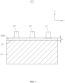
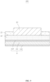
FIG. 1 is a schematic cross-sectional view of a battery according to an embodiment of this application. -
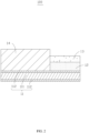
FIG. 2 is a schematic view of a cross section of the battery inFIG. 1 along a direction from an active material layer to a current collector. -
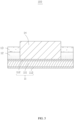
FIG. 3 is a schematic cross-sectional view of the battery inFIG. 2 according to another embodiment. -
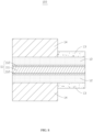
FIG. 4 is a schematic cross-sectional view of a battery according to another embodiment of this application. -
FIG. 5 is a schematic view of a cross section of the battery inFIG. 4 along a direction from an active material layer to a current collector. -
FIG. 6 is a schematic cross-sectional view of the battery inFIG. 5 in another embodiment. -
FIG. 7 is a schematic cross-sectional view of a battery according to still another embodiment of this application. -
FIG. 8 is a schematic cross-sectional view of the battery inFIG. 7 according to another embodiment. -
FIG. 9 is a schematic cross-sectional view of a battery according to yet another embodiment of this application. -
FIG. 10 is a schematic cross-sectional view of the battery inFIG. 9 according to another embodiment. -
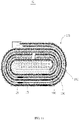
FIG. 11 is a schematic structural diagram of a cell according to an embodiment of this application. -
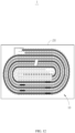
FIG. 12 is a schematic structural diagram of a battery according to an embodiment of this application. - This application will be further described with reference to the accompanying drawings in the following specific embodiments.
- The following clearly and completely describes the technical solutions in the embodiments of this application with reference to the accompanying drawings in the embodiments of this application. Apparently, the described embodiments are only some rather than all of the embodiments of this application. All other embodiments obtained by a person of ordinary skill in the art based on the embodiments of this application without creative efforts shall fall within the protection scope of this application.
- Unless otherwise defined, all technical and scientific terms used herein shall have the same meanings as commonly understood by those skilled in the art to which this application belongs. The terms used herein in the specification of this application are only used to describe specific embodiments and are not intended to limit this application.
- The following describes in detail some implementations of this application with reference to the accompanying drawings. Without conflicts, the following embodiments and features in the embodiments may be combined.
- Referring to
FIG. 1 andFIG. 2 , an embodiment of this application provides anelectrode plate 100. Theelectrode plate 100 includes acurrent collector 11. Thecurrent collector 11 includes amacromolecular polymer layer 111 and a firstconductive layer 112 The firstconductive layer 112 is disposed on a surface of themacromolecular polymer layer 111. Theelectrode plate 100 further includes a secondconductive layer 12. The secondconductive layer 12 is provided on a surface of the firstconductive layer 112 in anedge region 1001 in a widthwise direction (that is, an X-axis direction) of the electrode plate 100 (seeFIG. 1 andFIG. 4 ). The secondconductive layer 12 extends in a lengthwise direction (that is, a Y-axis direction) of theelectrode plate 100, and the firstconductive layer 112 is disposed between the secondconductive layer 12 and themacromolecular polymer layer 111. In this way, the secondconductive layer 12 and thecurrent collector 11 form a parallel structure, thereby effectively reducing resistance of theelectrode plate 100. - In this implementation, referring to
FIG. 2 , theelectrode plate 100 further includes aninsulation layer 13 provided on a surface of the secondconductive layer 12. The secondconductive layer 12 is disposed between the firstconductive layer 112 and theinsulation layer 13. - Further, referring to
FIG. 2 andFIG. 3 , anactive material layer 14 is provided on a surface of the firstconductive layer 112. Theactive material layer 14 connects with the secondconductive layer 12 and theinsulation layer 13. In an implementation, theactive material layer 14 only connects with the secondconductive layer 12; or a gap is present between theactive material layer 14 and the secondconductive layer 12 or between theactive material layer 14 and theinsulation layer 13. - In another implementation, referring to
FIG. 4 , in the widthwise direction of theelectrode plate 100, theedge region 1001 includes afirst edge region 1002 and asecond edge region 1003 opposite thefirst edge region 1002. Referring toFIGs. 7 to 10 , the secondconductive layer 12 extends from thefirst edge region 1002 to thesecond edge region 1003 of theelectrode plate 100. In this case, theactive material layer 14 is provided on a surface of the secondconductive layer 12. Theinsulation layer 13 is provided on a surface of the secondconductive layer 12 in thefirst edge region 1002 or thesecond edge region 1003 of theelectrode plate 100. Theactive material layer 14 connects with theinsulation layer 13. In another implementation, a gap is present between theactive material layer 14 and theinsulation layer 13. - The second
conductive layer 12 includes a conductive agent and a binder. A proportion of the conductive agent is 1%-80% and a proportion of the binder is 2%-60%. In this way, both good adhesion performance between the secondconductive layer 12 and thecurrent collector 11 and good conductive performance of the secondconductive layer 12 are ensured. The conductive agent includes one or more of carbon black particles, carbon nanotubes, graphite flakes, carbon fibers, acetylene black, metal particles, and metal nanowire. Optionally, the conductive agent includes metal nanowire. The metal nanowire is not limited to copper nanowire, silver nanowire, or the like. The binder may be polyvinylidene fluoride, polyacrylic acid, polyacrylate, polyacrylonitrile, polyurethane, acrylic resin, or modified materials thereof. Optionally, the binder is acrylic resin. - In this implementation, surface resistance of the second
conductive layer 12 is less than 1 Ω/cm2. In an implementation, surface resistance of the secondconductive layer 12 is less than or equal to 0.01 Ω/cm2. - In this implementation, adhesion between the second
conductive layer 12 and thecurrent collector 11 is greater than or equal to 10 N/m. In an implementation, adhesion between the secondconductive layer 12 and thecurrent collector 11 is greater than or equal to 50 N/m. - In this implementation, referring to
FIG. 2 , thickness T1 of the secondconductive layer 12 is 10 µm-100 µm. In an implementation, thickness T1 of the secondconductive layer 12 is 20 µm. - In this implementation, referring to
FIG. 2 , thickness T2 of the insulation layer is less than 20 µm. - Further, referring to
FIG. 1 andFIG. 2 , theelectrode plate 100 may also include atab 15. Thetab 15 connects with thecurrent collector 11. In this implementation, theelectrode plate 100 includes threetabs 15. In other implementations, the number oftabs 15 may be adaptively adjusted based on an actual need, which can be one, two, four, or other numbers. - Referring to
FIG. 11 , an embodiment of this application further provides acell 10. Thecell 10 includes anelectrode assembly 101. Theelectrode assembly 101 includes a positive-electrode plate and a negative-electrode plate. Theelectrode assembly 101 is formed by winding the positive-electrode plate and the negative-electrode plate. The positive-electrode plate and/or the negative-electrode plate include the foregoingelectrode plate 100. In this implementation, theelectrode assembly 101 further includes aseparator 102. Theseparator 102 is disposed between the positive electrode plate and the negative electrode plate. In other implementations, theelectrode assembly 101 may be formed by laminating the positive-electrode plate and the negative-electrode plate. - Referring to
FIG. 12 , an embodiment of this application further provides abattery 1. Thebattery 1 includes ahousing 20 and the foregoingcell 10. Thecell 10 is accommodated in thehousing 20. - The following describes the
electrode plate 100 and thecell 10 in this application in detail by using examples. It can be understood that sizes, materials and/or ratios of the current collector, the active material layer, the second conductive layer, the insulation layer, the separator, and so on in this application are not limited to content recorded in the description of the comparative examples and implementation examples, but may be selected specifically according to actual needs. - Referring to
FIG. 3 , anelectrode plate 100 includes acurrent collector 11, a secondconductive layer 12, aninsulation layer 13, and anactive material layer 14. In the widthwise direction of theelectrode plate 100, theedge region 1001 includes afirst edge region 1002 and asecond edge region 1003 opposite the first edge region 1002 (seeFIG. 4 ). - In example 1, referring to
FIG. 3 , thecurrent collector 11 includes amacromolecular polymer layer 111 and firstconductive layers 112 disposed on two sides of themacromolecular polymer layer 111. Referring toFIG. 1 andFIG. 3 , the secondconductive layer 12 is provided on a surface of the firstconductive layer 112 in thefirst edge region 1002, and the secondconductive layers 12 are located on two sides of thecurrent collector 11, respectively. Theinsulation layer 13 is provided on a surface of the secondconductive layer 12. Theactive material layer 14 is provided on a surface of the firstconductive layer 112 without the secondconductive layer 12. - In other implementations, referring to
FIG. 2 , the secondconductive layer 12, theinsulation layer 13, and theactive material layer 14 are disposed only on one side of thecurrent collector 11. - In example 1, the foregoing
electrode plate 100 was prepared by using the following method. - Provision of current collector 11: The
current collector 11 included amacromolecular polymer layer 111 and a firstconductive layers 112 disposed on two sides of themacromolecular polymer layer 111. - Preparation of electrode plate 100: Firstly, 10 g of acrylic resin was added into a mixing tank, and then a solvent N-methylpyrrolidone (NMP) was slowly added into the mixing tank so that the acrylic resin gradually dissolved into a glue solution. Then, 70 g of carbon nanotube powder was added into the mixing tank which had been vacuumed for 30 minutes, and a 50 minutes stir was given to form a uniform and stable conductive slurry. Next, an active coating was applied on a surface of the first
conductive layer 112 and dried for 30 minutes under 130°C to form anactive material layer 14, where the active coating was applied on both sides of thecurrent collector 11, without being applied on thefirst edge region 1002 on both sides of thecurrent collector 11. Then, the conductive slurry was applied evenly on a surface of the firstconductive layer 112 in thefirst edge region 1002 and dried for 30 minutes under 130°C to obtain a secondconductive layer 12 with a thickness T1 of 20 µm and a width W of 2 mm (seeFIG. 1 andFIG. 3 ); Finally, a ceramic coating was applied on a surface of the secondconductive layer 12 to form aninsulation layer 13 with a thickness T2 of 20 µm (seeFIG. 3 ). Theactive material layer 14 connects with the secondconductive layer 12 and theinsulation layer 13. - In example 1, adhesion between the second
conductive layer 12 and thecurrent collector 11 was 51 N/m. - Preparation of cell 10: Firstly, two of the foregoing
electrode plates 100 were taken respectively as a positive-electrode plate and a negative-electrode plate. Then, aseparator 102 was added between the positive-electrode plate and the negative-electrode plate, and the collection of the three was wound to a cell 10 (seeFIG. 11 ). - In example 1, internal resistance of the
cell 10 was 11.3 mΩ. - Example 2 differs from example 1 in mass of carbon nanotube powder contained in the conductive slurry. In example 2, the mass of the carbon nanotube powder was 80 g.
- In example 2, adhesion between the second
conductive layer 12 and thecurrent collector 11 was 32 N/m. Internal resistance of the cell was 11.5 mΩ. - Example 3 differs from example 1 in mass of acrylic resin contained in the conductive slurry. In example 3, the mass of acrylic resin was 3 g.
- In example 3, adhesion between the second
conductive layer 12 and thecurrent collector 11 was 9 N/m. Internal resistance of the cell was 14.1 mΩ. - Example 4 differs from example 1 in composition of the conductive slurry. In example 4, 70 g of copper nanowire powder was added into the mixing tank which had been vacuumed.
- In example 4, adhesion between the second
conductive layer 12 and thecurrent collector 11 was 54 N/m. Internal resistance of the cell was 10.5 mΩ. - Example 5 differs from example 1 in composition of the conductive slurry. In example 5, polyvinylidene fluoride was used to replace acrylic resin in example 1.
- In example 5, adhesion between the second
conductive layer 12 and thecurrent collector 11 was 7 N/m. Internal resistance of the cell was 15.5 mΩ. - Example 6 differs from example 1 in thickness of the second
conductive layer 12. In example 6, thickness of the secondconductive layer 12 T1 was 10 µm. - In example 6, adhesion between the second
conductive layer 12 and thecurrent collector 11 was 43 N/m. Internal resistance of the cell was 13.8 mΩ. - Example 7 differs from example 1 in width of the second
conductive layer 12. In example 7, width of the second conductive layer 12 W was 1 mm. - In example 7, adhesion between the second
conductive layer 12 and thecurrent collector 11 was 45 N/m. Internal resistance of thecell 10 was 15.1 mΩ. - Example 8 differs from example 1 in locations of the second
conductive layer 12, theactive material layer 14, and theinsulation layer 13. - Referring to
FIG. 4 andFIG. 6 , the secondconductive layer 12 was provided on a surface of the firstconductive layer 112 in theedge region 1002 and theedge region 1003. Theactive material layer 14 was provided on a surface of the firstconductive layer 112 without the secondconductive layer 12. Theinsulation layer 13 was provided on a surface of the secondconductive layer 12. The secondconductive layers 12 were disposed on two sides of thecurrent collector 11. In other implementations, referring toFIG. 5 , the secondconductive layer 12, theinsulation layer 13, and theactive material layer 14 were disposed only on one side of thecurrent collector 11. - In example 8, adhesion between the second
conductive layer 12 and thecurrent collector 11 was 54 N/m. Internal resistance of thecell 10 was 10.5 mΩ. - Example 9 differs from example 1 in locations of the second
conductive layer 12, theactive material layer 14, and theinsulation layer 13. - In example 9, referring to
FIG. 10 , the secondconductive layer 12 covered an entire surface of the firstconductive layer 112. Theinsulation layer 13 was provided on a surface of the secondconductive layer 12 in anedge region 1002 and on a surface of the secondconductive layer 12 in anedge region 1003. Theactive material layer 14 was provided on a surface of the secondconductive layer 12 without theinsulation layer 13. The secondconductive layers 12 were disposed on two sides of thecurrent collector 11, respectively. In an implementation, referring toFIG. 9 , the secondconductive layer 12, theinsulation layer 13, and theactive material layer 14 were disposed only on one side of thecurrent collector 11. - In another implementation, referring to
FIG. 8 , the secondconductive layer 12 covered an entire surface of the firstconductive layer 112. Theinsulation layer 13 was provided on a surface of the firstconductive layer 12 in anedge region 1002 or in anedge region 1003. Theactive material layer 14 was provided on a surface of the secondconductive layer 12 without theinsulation layer 13. The secondconductive layers 12 were disposed on two sides of thecurrent collector 11, respectively. In one other implementation, referring toFIG. 7 , the secondconductive layer 12, theinsulation layer 13, and theactive material layer 14 were disposed only on one side of thecurrent collector 11. - In example 9, preparation of the
electrode plate 100 was as follows: Firstly, 10 g of acrylic resin was added into a mixing tank, and then a solvent N-methylpyrrolidone (NMP) was slowly added into the mixing tank so that the acrylic resin gradually dissolved into a glue solution. Then, 70 g of carbon nanotube powder was added into the mixing tank which had been vacuumed for 30 minutes, and a 50 minutes stir was given to form a uniform and stable conductive slurry. Next, the conductive slurry was applied evenly on a surface of the firstconductive layer 112 and dried for 30 minutes under 130°C to form a secondconductive layer 12, where the conductive slurry was applied on both sides of thecurrent collector 11, full of a surface of the firstconductive layer 112. Then, an active coating was applied evenly on a surface of the secondconductive layer 12 and dried for 30 minutes under 130°C to form anactive material layer 14, where the active coating was applied on both sides of thecurrent collector 11 and applying the active coating on a surface of the secondconductive layer 12 in afirst edge region 1002 and asecond edge region 1003 were avoided. Finally, a ceramic coating was applied on a surface of the secondconductive layer 12 in afirst edge region 1002 and asecond edge region 1003 to form aninsulation layer 13 with a thickness T2 of 20 µm and a width W of 2 mm (seeFIG. 10 ). Theactive material layer 14 connected with theinsulation layer 13. - In example 9, adhesion between the second
conductive layer 12 and thecurrent collector 11 was 54 N/m. Internal resistance of the cell was 10.1 mΩ. - Comparative example 1 differs from example 1 in that the
electrode plate 100 in comparative example 1 did not have the secondconductive layer 12 or theinsulation layer 13. - In comparative example 1, internal resistance of the cell was 18.2 mΩ.
- Comparative example 2 differs from example 1 in that no carbon nanotube powder was contained in the conductive slurry.
- In comparative example 2, adhesion between the second
conductive layer 12 and thecurrent collector 11 was 80 N/m. Internal resistance of the cell was 18.3 mΩ. - Comparative example 3 differs from example 1 in that mass of carbon nanotube powder contained in the conductive slurry was 1 g.
- In comparative example 3, adhesion between the second
conductive layer 12 and thecurrent collector 11 was 74 N/m. Internal resistance of the cell was 17.2 mΩ. - Experimental parameters and test results of examples 1 to 9 and comparative examples 1 to 3 are given in Table 1.
Table 1 Group Binder Conductive agent Second conductive layer Adhesion between second conductive layer and current collector Internal resistance of cell Type Mass Type Mass Thickness Width Location Example 1 Acrylic resin 10 g Carbon nanotube 70 g 20 µm 2 mm First edge region 51 N/m 11.3 mΩ Example 2 Acrylic resin 10 g Carbon nanotube s 80 g 20 µm 2 mm First edge region 32 N/m 11.5 mΩ Example 3 Acrylic resin 3g Carbon nanotube s 70 g 20 µm 2 mm First edge region 9 N/m 14.1 mΩ Example 4 Acrylic resin 10 g Copper nanowire 70 g 20 µm 2 mm First edge region 54 N/m 10.5 mΩ Example 5 Polyvinylidene fluoride 10 g Carbon nanotube 70 g 20 µm 2 mm First edge region 7 N/m 15.5 mΩ Example 6 Acrylic resin 10 g Carbon nanotube 70 g 10 µm 2 mm First edge region 43 N/m 13.8 mΩ Example 7 Acrylic resin 10 g Carbon nanotube 70 g 20 µm 1 mm First edge region 45 N/m 15.1 mΩ Example 8 Acrylic resin 10 g Carbon nanotube 70 g 20 µm 2 mm First edge region and second edge region 54 N/m 10.5 mΩ Example 9 Acrylic resin 10 g Carbon nanotube 70 g 20 µm 2 mm The entire surface of first conductive layer 54 N/m 10.1 mΩ Comparative example 1 / / / / / / / / 18.2 mΩ Comparative example 2 Acrylic resin 10 g Carbon nanotube 0 20 µm 2 mm First edge region 80 N/m 18.3 mΩ Comparative example 3 Acrylic resin 10 g Carbon nanotube 1 g 20 µm 2 mm First edge region 74 N/m 17.2 mΩ - Table 1 shows that the amount and type of the conductive agent contained in the second
conductive layer 12 and thickness, width, and location of the secondconductive layer 12 all affected internal resistance of thecell 10. A comparison of examples 1-9 with comparative example 1 shows that the provision of the secondconductive layer 12 decreased internal resistance of thecell 10 greatly. In addition, the amount and type of the conductive agent in the secondconductive layer 12 and thickness, width, and location of the secondconductive layer 12 all affected adhesion between the secondconductive layer 12 and thecurrent collector 11. - In summary, in this application, the second
conductive layer 12 is disposed on theedge region 1001 or the entire surface of the firstconductive layer 112 in the widthwise direction of theelectrode plate 100, so that the secondconductive layer 12 and thecurrent collector 11 form a parallel structure, thereby effectively reducing resistance of theelectrode plate 100, which in turn decreases heat production and temperature rise of thecell 10 and thebattery 1 during charging and discharging, improving reliability of thecell 10 and thebattery 1 in use. Additionally, the secondconductive layer 12 being disposed on theedge region 1001 or the entire surface of the firstconductive layer 112 in the widthwise direction of theelectrode plate 100 allows electrons generated by theactive material layer 14 during charging and discharging to move to the secondconductive layer 12 through the firstconductive layer 112, which are then transferred rapidly along the lengthwise direction of theelectrode plate 100. This reduces resistance to transverse transport of electrons, improving transverse electron transport capacity of theelectrode plate 100, and thus effectively reducing resistance of thecell 10 and improving safety performance of thebattery 1 in use. - The foregoing embodiments are merely intended to describe the technical solutions of this application, but not to constitute any limitation. Although this application is described in detail with reference to preferred embodiments, persons of ordinary skill in the art should understand that modifications or equivalent replacements can be made to the technical solutions of this application, without departing from the spirit and essence of the technical solutions of this application.
| |
100 |
| |
1001 |
| |
1002 |
| |
1003 |
| |
11 |
| |
111 |
| First |
112 |
| Second |
12 |
| |
13 |
| |
14 |
| |
15 |
| |
1 |
| |
10 |
| |
101 |
| |
102 |
| |
20 |
Claims (12)
- An electrode plate, comprising a current collector, wherein the current collector comprises a macromolecular polymer layer and a first conductive layer, with the first conductive layer disposed on a surface of the macromolecular polymer layer, characterized in that a second conductive layer is provided on a surface of the first conductive layer in an edge region in a widthwise direction of the electrode plate, the second conductive layer extends in a lengthwise direction of the electrode plate, and the first conductive layer is disposed between the second conductive layer and the macromolecular polymer layer.
- The electrode plate according to claim 1, characterized in that an insulation layer is provided on a surface of the second conductive layer, and the second conductive layer is disposed between the first conductive layer and the insulation layer.
- The electrode plate according to claim 2, characterized in that an active material layer is provided on a surface of the first conductive layer, and the active material layer connects with the second conductive layer and the insulation layer.
- The electrode plate according to claim 1, characterized in that in the widthwise direction of the electrode plate, the edge region comprises a first edge region and a second edge region opposite the first edge region, and the second conductive layer extends from the first edge region of the electrode plate region to the second edge region of the electrode plate.
- The electrode plate according to claim 4, characterized in that an active material layer is provided on a surface of the second conductive layer, and an insulation layer is provided on a surface of the second conductive layer at the first region or the second region of the electrode plate.
- The electrode plate according to claim 5, characterized in that the active material layer connects with the insulation layer.
- The electrode plate according to any one of claims 1 to 6, characterized in that the second conductive layer comprises a conductive agent and a binder, wherein a proportion of the conductive agent is 1%-80% and a proportion of the binder is 2%-60%.
- The electrode plate according to claim 7, characterized in that surface resistance of the second conductive layer is less than 1 Ω/cm2.
- The electrode plate according to claim 7, characterized in that adhesion between the second conductive layer and the current collector is greater than or equal to 10 N/m.
- The electrode plate according to claim 7, characterized in that thickness of the second conductive layer is 10µm-100µm, and thickness of the insulation layer is less than 20µm.
- A cell comprising an electrode assembly, characterized in that the electrode assembly comprises the electrode plate according to any one of claims 1 to 10.
- A battery, comprising a cell and a housing configured to accommodate the cell, characterized in that the cell comprises the cell according to claim 11.
Applications Claiming Priority (1)
| Application Number | Priority Date | Filing Date | Title |
|---|---|---|---|
| PCT/CN2020/081622 WO2021189410A1 (en) | 2020-03-27 | 2020-03-27 | Pole piece, cell and battery |
Publications (2)
| Publication Number | Publication Date |
|---|---|
| EP4131508A1 true EP4131508A1 (en) | 2023-02-08 |
| EP4131508A4 EP4131508A4 (en) | 2024-08-28 |
Family
ID=77275575
Family Applications (1)
| Application Number | Title | Priority Date | Filing Date |
|---|---|---|---|
| EP20927603.9A Pending EP4131508A4 (en) | 2020-03-27 | 2020-03-27 | POLE PIECE, CELL AND BATTERY |
Country Status (3)
| Country | Link |
|---|---|
| EP (1) | EP4131508A4 (en) |
| CN (1) | CN113287214A (en) |
| WO (1) | WO2021189410A1 (en) |
Families Citing this family (4)
| Publication number | Priority date | Publication date | Assignee | Title |
|---|---|---|---|---|
| CN114566768A (en) * | 2022-02-10 | 2022-05-31 | 东莞新能安科技有限公司 | Pole piece, electrochemical device and electronic equipment |
| CN119601577A (en) * | 2023-09-08 | 2025-03-11 | 宁德时代新能源科技股份有限公司 | Pole piece, battery cell, battery, electrical equipment and method for preparing pole piece |
| CN117239058B (en) * | 2023-11-13 | 2024-03-01 | 珠海冠宇电池股份有限公司 | Pole piece, battery cell and battery |
| CN121215688B (en) * | 2025-11-27 | 2026-03-31 | 宁德时代新能源科技股份有限公司 | Battery cells, electrode assemblies, battery devices, and electrical appliances |
Family Cites Families (11)
| Publication number | Priority date | Publication date | Assignee | Title |
|---|---|---|---|---|
| CN101894937A (en) * | 2010-07-02 | 2010-11-24 | 东莞新能源科技有限公司 | Lithium ion battery and positive plate thereof |
| CN103181009B (en) * | 2010-10-27 | 2016-03-09 | 协立化学产业株式会社 | Conductivity primer composition |
| JP5614396B2 (en) * | 2011-10-26 | 2014-10-29 | トヨタ自動車株式会社 | Non-aqueous electrolyte secondary battery |
| KR102160273B1 (en) * | 2016-08-19 | 2020-09-25 | 주식회사 엘지화학 | Electrode for lithium secondary battery and Method for preparing the same |
| CN109873163B (en) * | 2017-12-05 | 2021-07-06 | 宁德时代新能源科技股份有限公司 | A current collector, its pole piece and battery and application |
| CN109873165B (en) * | 2017-12-05 | 2021-07-06 | 宁德时代新能源科技股份有限公司 | A current collector, its pole piece and battery |
| CN109873164B (en) * | 2017-12-05 | 2021-08-20 | 宁德时代新能源科技股份有限公司 | A current collector, its pole piece and electrochemical device |
| CN209045678U (en) * | 2018-11-05 | 2019-06-28 | 宁德新能源科技有限公司 | Anode pole piece, electrochemical appliance and the electronic device comprising it |
| CN112290029B (en) * | 2019-04-28 | 2022-04-22 | 宁德时代新能源科技股份有限公司 | Positive current collector, positive pole piece, electrochemical device, electric automobile and electronic product |
| CN110061182B (en) * | 2019-05-21 | 2020-12-01 | 宁德新能源科技有限公司 | Battery pole pieces and cells |
| CN111180738B (en) * | 2019-06-28 | 2021-07-30 | 宁德时代新能源科技股份有限公司 | An electrode pole piece and electrochemical device |
-
2020
- 2020-03-27 EP EP20927603.9A patent/EP4131508A4/en active Pending
- 2020-03-27 WO PCT/CN2020/081622 patent/WO2021189410A1/en not_active Ceased
- 2020-03-27 CN CN202080008069.2A patent/CN113287214A/en active Pending
Also Published As
| Publication number | Publication date |
|---|---|
| WO2021189410A1 (en) | 2021-09-30 |
| EP4131508A4 (en) | 2024-08-28 |
| CN113287214A (en) | 2021-08-20 |
Similar Documents
| Publication | Publication Date | Title |
|---|---|---|
| EP3907800B1 (en) | Negative electrode sheet, preparation method thereof and lithium ion battery containing the same | |
| EP4156319A1 (en) | High-load electrode, preparation method therefor, and lithium ion battery thereof | |
| KR20250078599A (en) | Negative electrode plate for sodium-ion battery, electrochemical apparatus, and electronic device | |
| CN109167020B (en) | Porous lithium ion pole piece with high energy density and preparation method thereof and lithium ion battery | |
| CN105958008B (en) | A kind of lithium ion battery anode composite piece, preparation method and lithium ion battery | |
| EP4131508A1 (en) | Pole piece, cell and battery | |
| CN111540882A (en) | A kind of negative pole piece, its preparation method and use | |
| JP4352475B2 (en) | Solid electrolyte secondary battery | |
| EP3767709A1 (en) | Positive electrode composition for lithium ion secondary cell, positive electrode for lithium ion secondary cell, and lithium ion secondary cell | |
| CN114512718B (en) | Composite solid electrolyte, preparation method thereof and high-performance all-solid battery | |
| JPH09213338A (en) | Battery and lithium-ion secondary battery | |
| CN116825962A (en) | Sodium ion battery composite negative electrode, battery and preparation method of negative electrode | |
| CN113013414B (en) | Cobalt-free positive electrode slurry, preparation method thereof, positive plate and lithium ion battery | |
| US20250006892A1 (en) | Methods of forming electrochemical cells with a combination formation charge rate | |
| KR20230027203A (en) | anode sheet and battery | |
| CN118782893A (en) | All-solid-state battery containing conductive polymer composite 3D spherical graphene aluminum-doped lithium zirconium oxygen solid electrolyte membrane and preparation method thereof | |
| WO2026002262A1 (en) | Positive electrode sheet, secondary battery, and electric device | |
| CN115241416A (en) | A kind of solid-state battery composite negative electrode and preparation method thereof | |
| EP4007033A1 (en) | All-solid-state laminated battery | |
| CN115117344A (en) | Silicon-based composite negative electrode material and preparation method thereof, and all-solid-state lithium battery | |
| US20240356004A1 (en) | Negative electrode plate and battery including the negative electrode plate | |
| CN219917211U (en) | Cathode pole piece structure and secondary battery | |
| KR102855155B1 (en) | An electrode for all solid state battery having improved interfacial properties | |
| CN115954467B (en) | Lithium metal negative electrode protective layer and preparation method thereof | |
| CN118248841A (en) | Electrode material for high temperature resistant secondary battery and preparation method thereof |
Legal Events
| Date | Code | Title | Description |
|---|---|---|---|
| STAA | Information on the status of an ep patent application or granted ep patent |
Free format text: STATUS: THE INTERNATIONAL PUBLICATION HAS BEEN MADE |
|
| PUAI | Public reference made under article 153(3) epc to a published international application that has entered the european phase |
Free format text: ORIGINAL CODE: 0009012 |
|
| STAA | Information on the status of an ep patent application or granted ep patent |
Free format text: STATUS: REQUEST FOR EXAMINATION WAS MADE |
|
| 17P | Request for examination filed |
Effective date: 20221026 |
|
| AK | Designated contracting states |
Kind code of ref document: A1 Designated state(s): AL AT BE BG CH CY CZ DE DK EE ES FI FR GB GR HR HU IE IS IT LI LT LU LV MC MK MT NL NO PL PT RO RS SE SI SK SM TR |
|
| DAV | Request for validation of the european patent (deleted) | ||
| DAX | Request for extension of the european patent (deleted) | ||
| A4 | Supplementary search report drawn up and despatched |
Effective date: 20240731 |
|
| RIC1 | Information provided on ipc code assigned before grant |
Ipc: H01M 4/13 20100101ALI20240725BHEP Ipc: H01M 4/66 20060101ALI20240725BHEP Ipc: H01M 4/64 20060101AFI20240725BHEP |