EP4131342A1 - Wide gap semiconductor device and method for manufacturing wide gap semiconductor device - Google Patents
Wide gap semiconductor device and method for manufacturing wide gap semiconductor device Download PDFInfo
- Publication number
- EP4131342A1 EP4131342A1 EP21775673.3A EP21775673A EP4131342A1 EP 4131342 A1 EP4131342 A1 EP 4131342A1 EP 21775673 A EP21775673 A EP 21775673A EP 4131342 A1 EP4131342 A1 EP 4131342A1
- Authority
- EP
- European Patent Office
- Prior art keywords
- layer
- region
- gap semiconductor
- wide gap
- lattice constant
- Prior art date
- Legal status (The legal status is an assumption and is not a legal conclusion. Google has not performed a legal analysis and makes no representation as to the accuracy of the status listed.)
- Granted
Links
Images




Classifications
-
- H—ELECTRICITY
- H10—SEMICONDUCTOR DEVICES; ELECTRIC SOLID-STATE DEVICES NOT OTHERWISE PROVIDED FOR
- H10D—INORGANIC ELECTRIC SEMICONDUCTOR DEVICES
- H10D62/00—Semiconductor bodies, or regions thereof, of devices having potential barriers
- H10D62/40—Crystalline structures
- H10D62/405—Orientations of crystalline planes
-
- H—ELECTRICITY
- H10—SEMICONDUCTOR DEVICES; ELECTRIC SOLID-STATE DEVICES NOT OTHERWISE PROVIDED FOR
- H10D—INORGANIC ELECTRIC SEMICONDUCTOR DEVICES
- H10D62/00—Semiconductor bodies, or regions thereof, of devices having potential barriers
- H10D62/80—Semiconductor bodies, or regions thereof, of devices having potential barriers characterised by the materials
- H10D62/83—Semiconductor bodies, or regions thereof, of devices having potential barriers characterised by the materials being Group IV materials, e.g. B-doped Si or undoped Ge
- H10D62/832—Semiconductor bodies, or regions thereof, of devices having potential barriers characterised by the materials being Group IV materials, e.g. B-doped Si or undoped Ge being Group IV materials comprising two or more elements, e.g. SiGe
- H10D62/8325—Silicon carbide
-
- H—ELECTRICITY
- H10—SEMICONDUCTOR DEVICES; ELECTRIC SOLID-STATE DEVICES NOT OTHERWISE PROVIDED FOR
- H10D—INORGANIC ELECTRIC SEMICONDUCTOR DEVICES
- H10D64/00—Electrodes of devices having potential barriers
- H10D64/01—Manufacture or treatment
- H10D64/011—Manufacture or treatment of electrodes ohmically coupled to a semiconductor
-
- H—ELECTRICITY
- H10—SEMICONDUCTOR DEVICES; ELECTRIC SOLID-STATE DEVICES NOT OTHERWISE PROVIDED FOR
- H10D—INORGANIC ELECTRIC SEMICONDUCTOR DEVICES
- H10D64/00—Electrodes of devices having potential barriers
- H10D64/01—Manufacture or treatment
- H10D64/012—Manufacture or treatment of electrodes comprising a Schottky barrier to a semiconductor
- H10D64/0121—Manufacture or treatment of electrodes comprising a Schottky barrier to a semiconductor to Group IV semiconductors
- H10D64/0122—Manufacture or treatment of electrodes comprising a Schottky barrier to a semiconductor to Group IV semiconductors to diamond, semiconducting diamond-like carbon or graphene
-
- H—ELECTRICITY
- H10—SEMICONDUCTOR DEVICES; ELECTRIC SOLID-STATE DEVICES NOT OTHERWISE PROVIDED FOR
- H10D—INORGANIC ELECTRIC SEMICONDUCTOR DEVICES
- H10D64/00—Electrodes of devices having potential barriers
- H10D64/01—Manufacture or treatment
- H10D64/012—Manufacture or treatment of electrodes comprising a Schottky barrier to a semiconductor
- H10D64/0121—Manufacture or treatment of electrodes comprising a Schottky barrier to a semiconductor to Group IV semiconductors
- H10D64/0123—Manufacture or treatment of electrodes comprising a Schottky barrier to a semiconductor to Group IV semiconductors to silicon carbide
-
- H—ELECTRICITY
- H10—SEMICONDUCTOR DEVICES; ELECTRIC SOLID-STATE DEVICES NOT OTHERWISE PROVIDED FOR
- H10D—INORGANIC ELECTRIC SEMICONDUCTOR DEVICES
- H10D64/00—Electrodes of devices having potential barriers
- H10D64/01—Manufacture or treatment
- H10D64/012—Manufacture or treatment of electrodes comprising a Schottky barrier to a semiconductor
- H10D64/0124—Manufacture or treatment of electrodes comprising a Schottky barrier to a semiconductor to Group III-V semiconductors
-
- H—ELECTRICITY
- H10—SEMICONDUCTOR DEVICES; ELECTRIC SOLID-STATE DEVICES NOT OTHERWISE PROVIDED FOR
- H10D—INORGANIC ELECTRIC SEMICONDUCTOR DEVICES
- H10D64/00—Electrodes of devices having potential barriers
- H10D64/60—Electrodes characterised by their materials
- H10D64/64—Electrodes comprising a Schottky barrier to a semiconductor
-
- H—ELECTRICITY
- H10—SEMICONDUCTOR DEVICES; ELECTRIC SOLID-STATE DEVICES NOT OTHERWISE PROVIDED FOR
- H10D—INORGANIC ELECTRIC SEMICONDUCTOR DEVICES
- H10D8/00—Diodes
- H10D8/01—Manufacture or treatment
- H10D8/051—Manufacture or treatment of Schottky diodes
-
- H—ELECTRICITY
- H10—SEMICONDUCTOR DEVICES; ELECTRIC SOLID-STATE DEVICES NOT OTHERWISE PROVIDED FOR
- H10D—INORGANIC ELECTRIC SEMICONDUCTOR DEVICES
- H10D8/00—Diodes
- H10D8/60—Schottky-barrier diodes
Definitions
- the present invention is related to wide gap semiconductor device and method for manufacturing wide gap semiconductor device.
- ⁇ Bn of SiC-SBD is generally controlled by a Schottky electrode, and Ti, Ni, Pt, or the like is used as the Schottky electrode of SiC-SBD.
- Ti is known to have the smallest ⁇ Bn, and most of commercially available n-type SiC-SBDs use Ti as the Schottky electrode.
- the present invention provides a wide gap semiconductor device capable of lowering ⁇ B without changing the material of a metal layer that has been conventionally used.
- a wide gap semiconductor device may comprise:
- the lattice constant L and the lattice constant L1 may be a lattice constant of C-axis.
- the single crystal layer in the interface region may include the first region at 20% or more.
- the single crystal layer in the interface region may include a first region made of Ti in which the lattice constant L1 is 0.235 nm or less.
- the single crystal layer in the interface region may include a first region made of Ti, in which the lattice constant L1 is 0.235 nm or less, at 20% or more.
- a wide gap semiconductor device may comprise steps of
- the second aspect of a manufacturing method of a wide gap semiconductor device according to the present invention may comprise steps of
- the third aspect of a manufacturing method of a wide gap semiconductor device according to the present invention may comprise steps of
- the fourth aspect of a manufacturing method of a wide gap semiconductor device according to the present invention may comprise steps of
- the interface region when an aspect is adopted in which: a single crystal layer is provided in an interface region having a thickness of up to 30 nm from the interface between a wide gap semiconductor layer and a metal layer; and when it is assumed that a lattice constant, in an equilibrium state, of the C-axis of a metal constituting the metal layer is L, the interface region includes first region in which a C-axis lattice constant L1 is smaller than L by 1.5% to 8%, ⁇ B can be lowered.
- one side means a front surface side that is the upper side in Fig. 1
- the other side means a back surface side that is the lower side in Fig. 1 .
- silicon carbide semiconductor device simply referred to as a "silicon carbide semiconductor device"
- silicon carbide semiconductor device simply referred to as a "silicon carbide semiconductor device”
- a special silicon carbide substrate may be adopted in which a single crystal silicon carbide layer is formed on polycrystalline silicon carbide.
- gallium nitride, gallium oxide, diamond, or the like may be used other than silicon carbide.
- the silicon carbide semiconductor device may have a silicon carbide substrate 11, a silicon carbide layer 12 provided on the one side (front surface side) of the silicon carbide substrate 11, and a metal electrode 20 that is a metal layer provided on the one side of the silicon carbide layer 12 to function as a front surface electrode.
- the silicon carbide layer 12 is directly provided on the silicon carbide substrate 11, and the metal electrode 20 is directly provided on the silicon carbide layer 12.
- the metal electrode 20 may have a single crystal layer 21 in an interface region at an interface with the silicon carbide layer 12.
- the single crystal layer 21 in the interface region may include first region in which a C-axis lattice constant is smaller than L by 1.5% to 8% (each having L1).
- the single crystal layer 21 may be formed by heteroepitaxial growth.
- the "interface region" in the metal electrode 20 means a region in the range of 30 nm from the interface between the metal electrode 20 and the silicon carbide layer 12, in the thickness direction, toward the metal electrode 20 (the one side).
- the metal electrode 20 may have a single crystal structure, a polycrystalline structure, or an amorphous structure.
- the metal electrode 20 may be provided with a connection electrode 40.
- the connection electrode 40 may be provided with a connection part 30.
- the connection part 30 may be a wire or a connecting body.
- connection electrode 40 may contain aluminum, an aluminum alloy containing silicon, an aluminum alloy containing copper, titanium, or the like, or may include a laminated film of an aluminum alloy containing silicon, an aluminum alloy containing copper, or aluminum and titanium. Without being limited thereto, the connection electrode 40 may contain another metal such as copper, gold, or nickel.
- a back surface electrode 50 may be provided on the other side (back surface side) of the silicon carbide semiconductor substrate 11.
- the back surface electrode 50 may contain nickel, titanium, or the like.
- An insulating layer 80, containing oxide or the like, may be provided in a region that is located on the one side (front surface side) of the silicon carbide layer 12 and in which a first electrode part 30 is not provided.
- the single crystal layer 21 in the interface region may include the first region, in which the C-axis lattice constant is L1, at 20% or more, or may include the first region at 30% or more thereof.
- "containing the first region at A% or more” means that when one image is captured with a TEM, the first region in which the lattice constant is L1 can be confirmed at A% or more in all region (see Fig. 9 ). However, whether or not the first region is at 20% or more included may be confirmed by capturing a plurality of images (e.g., 2 to 10 images) with a TEM and using measurement results in the plurality of images.
- Fig. 3 is a graph in which the cumulative probabilities of the C-axis lattice constant L1 are plotted.
- the graph shows that when annealing is performed at 450°C for 30 minutes in a vacuum state of 1E-4 Pa (1 ⁇ 10 -4 Pa), the probability that the C-axis lattice constant L1 is about 0.236 nm or less is less than 20%, whereas when annealing is performed at 350°C for 30 minutes in a vacuum state of 1E-4 Pa, the probability that the C-axis lattice constant L1 is about 0.233 nm or less is 30%.
- TEM is used for the measurement, and the result is obtained by cross-sectional diffraction images (see Fig. 9).
- FIG. 9 shows a cross-sectional TEM image at 600,000x magnification, a cross-sectional TEM image at 3,000,000x magnification, and a selected-area electron diffraction pattern.
- the lattice constant L1 of the single crystal can be measured from the selected-area electron diffraction pattern.
- the crystal structure of the silicon carbide layer 12 may have a hexagonal structure, or may have a hexagonal close-packed structure.
- the crystal structure of the metal electrode 20 may have a hexagonal structure, or may have a hexagonal close-packed structure.
- the metal of the metal electrode 20 in the interface region may contain Ti. However, without being limited thereto, the metal of the metal electrode 20 in the interface region may include a metal containing Ti as a main component, or may include Ni, Pt, Mo, a metal containing Ni as a main component, a metal containing Pt as a main component, or a metal containing Mo as a main component.
- the metal electrode 20 containing Ti or the metal electrode 20 including a metal containing Ti as a main component, and it is particularly advantageous to use the metal electrode 20 containing Ti.
- the term "main component” means that it occupies 50% or more in mass percent, and the metal containing Ti as a main component means a metal containing 50 mass% or more of Ti.
- a metal layer containing Ni, Al, or the like may be provided on the one side of the electrode containing Ti.
- the single crystal layer 21 in the interface region may include first region containing Ti in which the C-axis lattice constant L1 is 0.235 nm or less.
- a Ti layer is deposited on a substrate in which the silicon carbide layer 12 is provided on the silicon carbide substrate 11.
- electron beam deposition may be used, or sputtering may be used.
- a deposition rate is, for example, 0.1 to 0.3 nm/s (e.g., 0.12 nm/s), and the degree of vacuum at the time of the deposition of the Ti layer is, for example, 1E-4 Pa to 1E-5 Pa (e.g., 1E-4 Pa).
- the substrate provided with the Ti layer is annealed (heated) at 400°C or lower.
- the substrate provided with the Ti layer is annealed, for example, at 350°C for 30 minutes to 60 minutes (e.g., 30 minutes).
- the metal electrode 20 including the Ti layer is generated.
- vacancies are included in the Ti layer in the interface region between the silicon carbide layer 12 and the Ti layer.
- the Ti layer is annealed, crystallized of Ti proceeds while the vacancies are diffused outward. It is considered that when the annealing temperature is set to 450°C to 500°C, perfect crystal Ti (equilibrium state) is obtained, and the C-axis lattice constant increases (see Fig. 2(a) ). As a result, ⁇ Bn is saturated at a large value.
- the annealing is performed at 400°C or lower (e.g., 350°C) as in the present embodiment, the vacancies in the Ti layer are suppressed from being diffused outward, so that a state of including many vacancies can be realized. As a result, it is considered that stress is generated in the Ti layer, and the intervals between the Ti atoms tend to be uneven (see Fig. 2(b) ). Then, region (first region) in which a lattice constant is smaller than that at the time of complete crystallization and region (second region) in which a lattice constant is larger than that therein are both generated. When the number of the region (first region) in which a lattice constant is small is larger than the number of the region (second region) in which a lattice constant is large, ⁇ Bn can be lowered.
- Figs. 2 are simplified views for understanding the above description.
- the interatomic distances between the arranged constituent atoms are constant L, and the average lattice constant in the C-axis direction is L.
- the interatomic distances between the arranged constituent atoms are uneven by being divided into L1, L2, and L.
- L1 is smaller than L.
- L2 is larger than L.
- the average lattice constant of the lattice constants in the C-axis direction is L in this region.
- the interatomic distances between the arranged constituent atoms are uneven by being divided into L1 and L.
- L1 is smaller than L. Therefore, the average lattice constant of the lattice constants in the C-axis direction is smaller than L in this region.
- the average lattice constant of the lattice constants in the C-axis direction is smaller than L in this region.
- the interatomic distances between the arranged constituent atoms are uneven by being divided into L1 and L.
- L1 is smaller than L. Therefore, the average lattice constant of the lattice constants in the C-axis direction is smaller than L in this region.
- Fig. 3 shows that when annealing is performed at 400°C or lower (here, 350°C), region (second region) in which the lattice constant in the C-axis direction is large exist (a plot exists at a location where the C-axis lattice constant is about 0.2425 nm), but region (first region) in which the lattice constant is small also exist (a plot also exists at a location where the C-axis lattice constant is about 0.2306 nm).
- the lattice constant decreases by the fact that when one image is captured with TEM, the first region occupies a wider region than the second region.
- the first region occupies a wider region than the second region by capturing a plurality of images (e.g., 2 to 10 images) with TEM and using measurement results in the plurality of images.
- ⁇ Bn also decreased when the annealing was performed at 550°C or higher
- Fig. 6 when the annealing was performed at 550°C or higher, the n value (ideal factor) was deteriorated. This is considered to be because a chemical reaction occurs between the Ti layer and the silicon carbide layer 12.
- the value (C-axis lattice constant) on the horizontal axis shown in Fig. 6 also represents a lattice constant when the cumulative probability is 30%, similarly to Fig. 4 .
- a Ti layer is deposited on a substrate in which the silicon carbide layer 12 is provided on the silicon carbide substrate 11.
- electron beam deposition may be used, or sputtering may be used.
- a deposition rate is, for example, 0.1 to 0.3 nm/s (e.g., 0.12 nm/s), and the degree of vacuum at the time of the deposition of the Ti layer is, for example, 1E-4 Pa to 1E-5 Pa (e.g., 1E-4 Pa).
- Fig. 7 is a graph showing a relationship between an annealing time when annealing is performed at 450°C and ⁇ Bn (eV), and it can be confirmed that ⁇ Bn (eV) decreases when the annealing time is short.
- a Ti layer is deposited on a substrate in which the silicon carbide layer 12 is provided on the silicon carbide substrate 11, similarly to the manufacturing examples 1 and 2.
- electron beam deposition may be used, or sputtering may be used.
- a deposition rate in the manufacturing example 3 is set to be less than 0.02 nm/s.
- the deposition rate may be, for example, 0.01 nm/s or less (e.g., 0.01 nm/s)
- the degree of vacuum at the time of the deposition of the Ti layer is, for example, 1E-4 Pa to 1E-5 Pa (e.g., 1E-4 Pa).
- the substrate provided with the Ti layer is annealed (heated) at 450 to 500°C.
- the substrate provided with the Ti layer is annealed, for example, at 450°C for 30 minutes to 60 minutes (e.g., 30 minutes).
- the probability that molecules, atoms, ions, and the like other than Ti fly to the front surface of the silicon carbide layer 12 at the time of the deposition relatively increases. Therefore, a state is created in which more vacancies are included in the Ti layer at the interface between the Ti layer and the silicon carbide layer 12. Therefore, even when the annealing temperature is set to 450°C to 500°C and the annealing time is set to 30 minutes, more vacancies remain in the Ti layer. Therefore, region in which a lattice constant is smaller than that at the time of complete crystallization can be formed by generating stress, and ⁇ B can be lowered.
- a Ti layer is deposited on a substrate in which the silicon carbide layer 12 is provided on the silicon carbide substrate 11, similarly to the manufacturing examples 1 to 3.
- electron beam deposition may be used, or sputtering may be used.
- the degree of vacuum at the time of the deposition in the manufacturing example 4 is set to 5E-4 Pa or more.
- a deposition rate is, for example, 0.1 to 0.3 nm/s (e.g., 0.12 nm/s)
- the degree of vacuum at the time of the deposition of the Ti layer is 5E-4 Pa or more (e.g., 9.3E-4 Pa). If the degree of vacuum is excessively increased, various problems occur, and thus the upper limit value is 1E-2 Pa.
- the substrate provided with the Ti layer is annealed (heated) at 450 to 500°C.
- the substrate provided with the Ti layer is annealed, for example, at 450°C for 30 minutes to 60 minutes (e.g., 30 minutes).
- the single crystal layer 21 in the interface region of the metal electrode 20 includes first region in which the C-axis lattice constant L1 is smaller than the lattice constant L in an equilibrium state by 1.5% to 8%, ⁇ Bn can be lowered without changing the material of the metal electrode 20.
- the single crystal layer 21 in the interface region includes the first region, in which the C-axis lattice constant is L1 (value smaller than L by 1.5% to 8%), at 20% or more, ⁇ Bn can be lowered more reliably.
- the single crystal layer 21 in the interface region includes the first region, in which the C-axis lattice constant is L1 (value smaller than L by 1.5% to 8%), at 30% or more, ⁇ Bn can be lowered even more reliably (see Fig. 3 and Fig. 4 ).
- ⁇ Bn can be lowered more reliably.
- the originally low ⁇ Bn can be further lowered, and when the single crystal layer includes the first region containing Ti in which the C-axis lattice constant L1 is 0.235 nm or less, ⁇ Bn can be lowered more reliably.
Landscapes
- Electrodes Of Semiconductors (AREA)
- Surface Acoustic Wave Elements And Circuit Networks Thereof (AREA)
Abstract
Description
- The present invention is related to wide gap semiconductor device and method for manufacturing wide gap semiconductor device.
- Conventionally, a wide gap semiconductor device using silicon carbide or the like has been known (see, for example,
Japanese Patent Application Laid-Open No. 2015 - 56543 - When n-type silicon carbide, which is a kind of wide gap semiconductor device, is taken as an example, ϕBn of SiC-SBD is generally controlled by a Schottky electrode, and Ti, Ni, Pt, or the like is used as the Schottky electrode of SiC-SBD. Among them, Ti is known to have the smallest ϕBn, and most of commercially available n-type SiC-SBDs use Ti as the Schottky electrode.
- If the conventionally used electrode is changed, an etching step needs to be changed in addition to a deposition step itself. Therefore, there is a demand to lower ϕB without changing the material of the SBD electrode.
- The present invention provides a wide gap semiconductor device capable of lowering ϕB without changing the material of a metal layer that has been conventionally used.
- A wide gap semiconductor device may comprise:
- a wide gap semiconductor layer; and
- a metal layer provided on the wide gap semiconductor layer,
- wherein the metal layer has a single crystal layer in an interface region at an interface with the wide gap semiconductor layer,
- when it is assumed that a lattice constant, in an equilibrium state, of a metal constituting the metal layer is L, the single crystal layer in the interface region includes a first region in which a lattice constant L1 is smaller than L by 1.5% to 8%.
- In the wide gap semiconductor device according to
concept 1,
the lattice constant L and the lattice constant L1 may be a lattice constant of C-axis. - In the wide gap semiconductor device according to
concept 1 or 2,
the single crystal layer in the interface region may include the first region at 20% or more. - In the wide gap semiconductor device according to any one of
concepts 1 to 3, - the single crystal layer in the interface region may include a second region in which the lattice constant L1 is larger than L, and
- the first region may occupy a wider region than the second region in the interface region.
- In the wide gap semiconductor device according to any one of
concepts 1 to 4, - the wide gap semiconductor layer may be a silicon carbide layer having a hexagonal structure,
- a crystal structure of the metal layer may have a hexagonal structure, and
- the metal of the metal layer may be Ti.
- In the wide gap semiconductor device according to
concept 5,
the single crystal layer in the interface region may include a first region made of Ti in which the lattice constant L1 is 0.235 nm or less. - In the wide gap semiconductor device according to
concept 6,
the single crystal layer in the interface region may include a first region made of Ti, in which the lattice constant L1 is 0.235 nm or less, at 20% or more. - A wide gap semiconductor device according to the present invention may comprise steps of
- depositing a Ti layer on a wide gap semiconductor layer; and
- heating the Ti layer at 400°C or lower,
- wherein the Ti layer has the single crystal layer in an interface region at an interface between the wide gap semiconductor layer and the Ti layer.
- The second aspect of a manufacturing method of a wide gap semiconductor device according to the present invention may comprise steps of
- depositing a Ti layer on a wide gap semiconductor layer; and
- heating the Ti layer for between 2 minutes and 10 minutes;
- wherein the Ti layer may have a single crystal layer in an interface region at an interface between the wide gap semiconductor layer ant the Ti layer.
- The third aspect of a manufacturing method of a wide gap semiconductor device according to the present invention may comprise steps of
- depositing a Ti layer on a wide gap semiconductor layer at a depositing rate of less than 0.02 nm/s; and
- heating the Ti layer;
- wherein the Ti layer may have a single crystal layer in an interface region at an interface between the wide gap semiconductor layer ant the Ti layer.
- The fourth aspect of a manufacturing method of a wide gap semiconductor device according to the present invention may comprise steps of
- depositing a Ti layer on a wide gap semiconductor layer with a degree of vacuum of 5E-4Pa or more; and
- heating the Ti layer;
- wherein the Ti layer may have a single crystal layer in an interface region at an interface between the wide gap semiconductor layer ant the Ti layer.
- In the present invention, when an aspect is adopted in which: a single crystal layer is provided in an interface region having a thickness of up to 30 nm from the interface between a wide gap semiconductor layer and a metal layer; and when it is assumed that a lattice constant, in an equilibrium state, of the C-axis of a metal constituting the metal layer is L, the interface region includes first region in which a C-axis lattice constant L1 is smaller than L by 1.5% to 8%, ϕB can be lowered.
-
-
Fig. 1 is a side sectional view of an n-type silicon carbide semiconductor device that can be used in an embodiment of the present invention. -
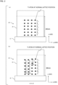
Fig. 2(a) is a side sectional view showing an aspect in which intervals between constituent atoms are uniform in a single crystal layer, andFig. 2(b) is a side sectional view showing an aspect in which intervals between constituent atoms are not uniform in a single crystal layer. -
Fig. 3 is a graph showing a relationship between a C-axis lattice constant L1 in a single crystal layer containing Ti and a cumulative probability plot in an aspect in which annealing temperatures of Ti are different. -
Fig. 4 is a graph showing a relationship between the C-axis lattice constant L1 in the single crystal layer containing Ti and ϕBn (eV) in an n-type silicon carbide device. -
Fig. 5 is a graph showing a relationship between the C-axis lattice constant L1 in the single crystal layer containing Ti and Ef (eV) in a silicon carbide device, the relationship being obtained by theoretical calculations. -
Fig. 6 is a graph showing a relationship between the C-axis lattice constant L1 in the single crystal layer containing Ti and an n value in the silicon carbide device. -
Fig. 7 is a graph showing a relationship between an annealing time of a metal electrode containing Ti at 450°C and ϕBn (eV) in a manufactured n-type silicon carbide device. -
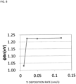
Fig. 8 is a graph showing a relationship between a Ti deposition rate and ϕBn (eV) in the manufactured n-type silicon carbide device. -
Fig. 9 are images respectively showing a cross-sectional TEM image at 600,000× magnification, a cross-sectional TEM image at 3,000,000x magnification, and a selected-area electron diffraction pattern. - In the present embodiment, "one side" means a front surface side that is the upper side in
Fig. 1 , and "the other side" means a back surface side that is the lower side inFig. 1 . - The present embodiment will be described by using an n-type silicon carbide semiconductor device (hereinafter, simply referred to as a "silicon carbide semiconductor device") as an example of a wide gap semiconductor device, but the present invention is not limited thereto. A special silicon carbide substrate may be adopted in which a single crystal silicon carbide layer is formed on polycrystalline silicon carbide. As the wide gap semiconductor, gallium nitride, gallium oxide, diamond, or the like may be used other than silicon carbide.
- As shown in
Fig. 1 , the silicon carbide semiconductor device may have asilicon carbide substrate 11, asilicon carbide layer 12 provided on the one side (front surface side) of thesilicon carbide substrate 11, and ametal electrode 20 that is a metal layer provided on the one side of thesilicon carbide layer 12 to function as a front surface electrode. Note that as an example in the aspect shown inFig. 1 , thesilicon carbide layer 12 is directly provided on thesilicon carbide substrate 11, and themetal electrode 20 is directly provided on thesilicon carbide layer 12. As shown inFigs. 2(a) and 2(b) , themetal electrode 20 may have asingle crystal layer 21 in an interface region at an interface with thesilicon carbide layer 12. When it is assumed that a lattice constant, in an equilibrium state, of the C-axis of a metal constituting themetal electrode 20 is L, thesingle crystal layer 21 in the interface region may include first region in which a C-axis lattice constant is smaller than L by 1.5% to 8% (each having L1). Thesingle crystal layer 21 may be formed by heteroepitaxial growth. - In the present embodiment, the "interface region" in the
metal electrode 20 means a region in the range of 30 nm from the interface between themetal electrode 20 and thesilicon carbide layer 12, in the thickness direction, toward the metal electrode 20 (the one side). On the further one side of the interface region of themetal electrode 20, themetal electrode 20 may have a single crystal structure, a polycrystalline structure, or an amorphous structure. - As shown in
Fig. 1 , themetal electrode 20 may be provided with aconnection electrode 40. In addition, theconnection electrode 40 may be provided with aconnection part 30. Theconnection part 30 may be a wire or a connecting body. - The
connection electrode 40 may contain aluminum, an aluminum alloy containing silicon, an aluminum alloy containing copper, titanium, or the like, or may include a laminated film of an aluminum alloy containing silicon, an aluminum alloy containing copper, or aluminum and titanium. Without being limited thereto, theconnection electrode 40 may contain another metal such as copper, gold, or nickel. - A
back surface electrode 50 may be provided on the other side (back surface side) of the siliconcarbide semiconductor substrate 11. Theback surface electrode 50 may contain nickel, titanium, or the like. An insulatinglayer 80, containing oxide or the like, may be provided in a region that is located on the one side (front surface side) of thesilicon carbide layer 12 and in which afirst electrode part 30 is not provided. - The
single crystal layer 21 in the interface region may include the first region, in which the C-axis lattice constant is L1, at 20% or more, or may include the first region at 30% or more thereof. In the present embodiment, "containing the first region at A% or more" means that when one image is captured with a TEM, the first region in which the lattice constant is L1 can be confirmed at A% or more in all region (seeFig. 9 ). However, whether or not the first region is at 20% or more included may be confirmed by capturing a plurality of images (e.g., 2 to 10 images) with a TEM and using measurement results in the plurality of images. - When the metal contains Ti, the lattice constant L in an equilibrium state is 0.24 nm. Therefore, the fact that the C-axis lattice constant L1 is smaller than L by 1.5% to 8% means that the C-axis lattice constant L1 falls within the range of 0.2208 nm to 0.2364 nm.
Fig. 3 is a graph in which the cumulative probabilities of the C-axis lattice constant L1 are plotted. The graph shows that when annealing is performed at 450°C for 30 minutes in a vacuum state of 1E-4 Pa (1 × 10⁻⁴ Pa), the probability that the C-axis lattice constant L1 is about 0.236 nm or less is less than 20%, whereas when annealing is performed at 350°C for 30 minutes in a vacuum state of 1E-4 Pa, the probability that the C-axis lattice constant L1 is about 0.233 nm or less is 30%. TEM is used for the measurement, and the result is obtained by cross-sectional diffraction images (seeFig. 9). Fig. 9 shows a cross-sectional TEM image at 600,000x magnification, a cross-sectional TEM image at 3,000,000x magnification, and a selected-area electron diffraction pattern. The lattice constant L1 of the single crystal can be measured from the selected-area electron diffraction pattern. - As confirmed by the inventors, it is found, as shown in
Fig. 4 , that ϕBn (eV) decreases as the C-axis lattice constant L1 decreases. It has also been confirmed, as shown inFig. 5 , that as a result of verification by first-principles calculations, the Fermi level (Ef) changes in a direction of lowering ϕBn by reducing the lattice constant. The value (C-axis lattice constant) on the horizontal axis shown inFig. 4 represents a lattice constant when the cumulative probability is 30%. Note that there is the relationship that the larger Ef (eV), the smaller ϕBn (eV). - The crystal structure of the
silicon carbide layer 12 may have a hexagonal structure, or may have a hexagonal close-packed structure. The crystal structure of themetal electrode 20 may have a hexagonal structure, or may have a hexagonal close-packed structure. The metal of themetal electrode 20 in the interface region may contain Ti. However, without being limited thereto, the metal of themetal electrode 20 in the interface region may include a metal containing Ti as a main component, or may include Ni, Pt, Mo, a metal containing Ni as a main component, a metal containing Pt as a main component, or a metal containing Mo as a main component. However, from the viewpoint that ϕBn can be lowered to a small value, it is advantageous to use themetal electrode 20 containing Ti or themetal electrode 20 including a metal containing Ti as a main component, and it is particularly advantageous to use themetal electrode 20 containing Ti. Note that the term "main component" means that it occupies 50% or more in mass percent, and the metal containing Ti as a main component means a metal containing 50 mass% or more of Ti. - Even when the metal of the
metal electrode 20 in the interface region contains Ti, a metal layer containing Ni, Al, or the like may be provided on the one side of the electrode containing Ti. - The
single crystal layer 21 in the interface region may include first region containing Ti in which the C-axis lattice constant L1 is 0.235 nm or less. - Next, an example of a manufacturing method will be described. In the following manufacturing example, an aspect will be described in which Ti is used as the
metal electrode 20. - A Ti layer is deposited on a substrate in which the
silicon carbide layer 12 is provided on thesilicon carbide substrate 11. For the deposition of the Ti layer, electron beam deposition may be used, or sputtering may be used. A deposition rate is, for example, 0.1 to 0.3 nm/s (e.g., 0.12 nm/s), and the degree of vacuum at the time of the deposition of the Ti layer is, for example, 1E-4 Pa to 1E-5 Pa (e.g., 1E-4 Pa). - Next, the substrate provided with the Ti layer is annealed (heated) at 400°C or lower. The substrate provided with the Ti layer is annealed, for example, at 350°C for 30 minutes to 60 minutes (e.g., 30 minutes). As a result, the
metal electrode 20 including the Ti layer is generated. - Immediately after the Ti layer is deposited on the
silicon carbide layer 12, vacancies are included in the Ti layer in the interface region between thesilicon carbide layer 12 and the Ti layer. When the Ti layer is annealed, crystallized of Ti proceeds while the vacancies are diffused outward. It is considered that when the annealing temperature is set to 450°C to 500°C, perfect crystal Ti (equilibrium state) is obtained, and the C-axis lattice constant increases (seeFig. 2(a) ). As a result, ϕBn is saturated at a large value. - On the other hand, when the annealing is performed at 400°C or lower (e.g., 350°C) as in the present embodiment, the vacancies in the Ti layer are suppressed from being diffused outward, so that a state of including many vacancies can be realized. As a result, it is considered that stress is generated in the Ti layer, and the intervals between the Ti atoms tend to be uneven (see
Fig. 2(b) ). Then, region (first region) in which a lattice constant is smaller than that at the time of complete crystallization and region (second region) in which a lattice constant is larger than that therein are both generated. When the number of the region (first region) in which a lattice constant is small is larger than the number of the region (second region) in which a lattice constant is large, ϕBn can be lowered. - Here,
Figs. 2 are simplified views for understanding the above description. In a region including the atoms arranged on the right-most inFig. 2(b) , the interatomic distances between the arranged constituent atoms are constant L, and the average lattice constant in the C-axis direction is L. In a region including the atoms arranged second from the right inFig. 2(b) , the interatomic distances between the arranged constituent atoms are uneven by being divided into L1, L2, and L. L1 is smaller than L. L2 is larger than L. However, since the number of the regions, in each of which the interatomic distances are L1, and the number of the regions, in each of which the interatomic distances are L2, are equal, the average lattice constant of the lattice constants in the C-axis direction is L in this region. In a region including the atoms arranged third from the right inFig. 2(b) , the interatomic distances between the arranged constituent atoms are uneven by being divided into L1 and L. L1 is smaller than L. Therefore, the average lattice constant of the lattice constants in the C-axis direction is smaller than L in this region. In a region including the atoms arranged fourth from the right inFig. 2(b) , the interatomic distances between the arranged constituent atoms are uneven by being divided into L1 and L. L1 is smaller than L. Therefore, the average lattice constant of the lattice constants in the C-axis direction is smaller than L in this region. - As a result, when the aspect of
Fig. 2(b) is viewed as a whole, the average lattice constant in the C-axis direction is smaller than L.Fig. 3 can be said to show an actual measurement result supporting this.Fig. 3 shows that when annealing is performed at 400°C or lower (here, 350°C), region (second region) in which the lattice constant in the C-axis direction is large exist (a plot exists at a location where the C-axis lattice constant is about 0.2425 nm), but region (first region) in which the lattice constant is small also exist (a plot also exists at a location where the C-axis lattice constant is about 0.2306 nm). And, it is shown that the number of the region (second region), in which the lattice constant is large, is smaller than the number of region (first region) in which the lattice constant is small. That is, the lattice constant in the C-axis direction decreases on average. As a result, ϕBn decreases as described above. - It can also be confirmed that the lattice constant decreases by the fact that when one image is captured with TEM, the first region occupies a wider region than the second region. Alternatively, it may also be confirmed that the first region occupies a wider region than the second region by capturing a plurality of images (e.g., 2 to 10 images) with TEM and using measurement results in the plurality of images.
- Note that as shown in
Fig. 4 , it could be confirmed that ϕBn also decreased when the annealing was performed at 550°C or higher, while as shown inFig. 6 , when the annealing was performed at 550°C or higher, the n value (ideal factor) was deteriorated. This is considered to be because a chemical reaction occurs between the Ti layer and thesilicon carbide layer 12. The value (C-axis lattice constant) on the horizontal axis shown inFig. 6 also represents a lattice constant when the cumulative probability is 30%, similarly toFig. 4 . - Next, another manufacturing example different from the above will be described. Similarly to the manufacturing example 1, a Ti layer is deposited on a substrate in which the
silicon carbide layer 12 is provided on thesilicon carbide substrate 11. For the deposition of the Ti layer, electron beam deposition may be used, or sputtering may be used. A deposition rate is, for example, 0.1 to 0.3 nm/s (e.g., 0.12 nm/s), and the degree of vacuum at the time of the deposition of the Ti layer is, for example, 1E-4 Pa to 1E-5 Pa (e.g., 1E-4 Pa). - Next, the substrate provided with the Ti layer is annealed (heated) at 450°C to 500°C. The substrate provided with the Ti layer is annealed, for example, at 450°C for between 2 minutes and 10 minutes (inclusive) (e.g., 8 minutes).
Fig. 7 is a graph showing a relationship between an annealing time when annealing is performed at 450°C and ϕBn (eV), and it can be confirmed that ϕBn (eV) decreases when the annealing time is short. - As described above, immediately after the Ti layer is deposited on the
silicon carbide layer 12, a state is created at the interface between thesilicon carbide layer 12 and the Ti layer, in which vacancies are included in the Ti layer. When the Ti layer is annealed, crystallized of Ti proceeds while the vacancies in the Ti layer are diffused outward. In this respect, even when annealing is performed at 450 to 500°C, the vacancies in the Ti layer are suppressed from being diffused outward by shortening the annealing time. Therefore, a state in which many vacancies are included in the Ti layer can be realized, and region, in which a lattice constant is smaller than that at the time of complete crystallization, can be formed by generating stress. As a result, ϕBn can be lowered. - Next, a manufacturing example 3 different from the above manufacturing examples 1 and 2 will be described.
- Also in the manufacturing example 3, a Ti layer is deposited on a substrate in which the
silicon carbide layer 12 is provided on thesilicon carbide substrate 11, similarly to the manufacturing examples 1 and 2. For the deposition of the Ti layer, electron beam deposition may be used, or sputtering may be used. However, a deposition rate in the manufacturing example 3 is set to be less than 0.02 nm/s. For example, the deposition rate may be, for example, 0.01 nm/s or less (e.g., 0.01 nm/s), and the degree of vacuum at the time of the deposition of the Ti layer is, for example, 1E-4 Pa to 1E-5 Pa (e.g., 1E-4 Pa). - Next, the substrate provided with the Ti layer is annealed (heated) at 450 to 500°C. The substrate provided with the Ti layer is annealed, for example, at 450°C for 30 minutes to 60 minutes (e.g., 30 minutes).
- By reducing the deposition rate as in the present manufacturing example, the probability that molecules, atoms, ions, and the like other than Ti fly to the front surface of the
silicon carbide layer 12 at the time of the deposition relatively increases. Therefore, a state is created in which more vacancies are included in the Ti layer at the interface between the Ti layer and thesilicon carbide layer 12. Therefore, even when the annealing temperature is set to 450°C to 500°C and the annealing time is set to 30 minutes, more vacancies remain in the Ti layer. Therefore, region in which a lattice constant is smaller than that at the time of complete crystallization can be formed by generating stress, and ϕB can be lowered. - The results of changing, by the inventors of the present application, the deposition rate under conditions in which the annealing is performed at 450°C for 30 minutes are as shown in Table 1 below. These results are shown in
Fig. 8 .[Table 1] Degree of vacuum (Pa) Deposition rate (nm/s) ϕBn (eV) 1.00E-04 0.01 1.031 1.00E-04 0.02 1.224 1.00E-04 0.05 1.223 1.00E-04 0.12 1.226 - Next, a manufacturing example 4 different from the manufacturing examples 1 to 3 will be described.
- Also in the manufacturing example 4, a Ti layer is deposited on a substrate in which the
silicon carbide layer 12 is provided on thesilicon carbide substrate 11, similarly to the manufacturing examples 1 to 3. For the deposition of the Ti layer, electron beam deposition may be used, or sputtering may be used. However, the degree of vacuum at the time of the deposition in the manufacturing example 4 is set to 5E-4 Pa or more. For example, a deposition rate is, for example, 0.1 to 0.3 nm/s (e.g., 0.12 nm/s), and the degree of vacuum at the time of the deposition of the Ti layer is 5E-4 Pa or more (e.g., 9.3E-4 Pa). If the degree of vacuum is excessively increased, various problems occur, and thus the upper limit value is 1E-2 Pa. - Next, the substrate provided with the Ti layer is annealed (heated) at 450 to 500°C. The substrate provided with the Ti layer is annealed, for example, at 450°C for 30 minutes to 60 minutes (e.g., 30 minutes).
- By increasing the degree of vacuum as in the present manufacturing example, the probability that molecules, atoms, ions, and the like other than Ti fly to the front surface of the
silicon carbide layer 12 at the time of the deposition relatively increases. Therefore, a state is created in which more vacancies are included in the Ti layer at the interface between the Ti layer and thesilicon carbide layer 12. Therefore, even when the annealing temperature is set to 450 to 500°C and the annealing time is set to 30 minutes, more vacancies remain in the Ti layer. Therefore, region in which a lattice constant is smaller than that at the time of complete crystallization can be formed by generating stress, and ϕBn can be lowered. - The results of the inventors of the present application setting the degree of vacuum to 9.3E-4 Pa under conditions in which the annealing is performed at 450°C for 30 minutes are as shown in Table 2 below, and it could be confirmed that ϕBn could be lowered.
[Table 2] Degree of vacuum (Pa) Deposition rate (nm/s) ϕBn (eV) 9.30E-04 0.12 1.18 - Next, effects of the present embodiment having the above-described configuration will be described. Note that all aspects described in the "effects" can be adopted in the above configuration.
- In the present embodiment, when an aspect is adopted in which the
single crystal layer 21 in the interface region of themetal electrode 20 includes first region in which the C-axis lattice constant L1 is smaller than the lattice constant L in an equilibrium state by 1.5% to 8%, ϕBn can be lowered without changing the material of themetal electrode 20. - When the
single crystal layer 21 in the interface region includes the first region, in which the C-axis lattice constant is L1 (value smaller than L by 1.5% to 8%), at 20% or more, ϕBn can be lowered more reliably. In addition, when thesingle crystal layer 21 in the interface region includes the first region, in which the C-axis lattice constant is L1 (value smaller than L by 1.5% to 8%), at 30% or more, ϕBn can be lowered even more reliably (seeFig. 3 andFig. 4 ). - When the
metal electrode 20 in the interface region contains hexagonal Ti and thesilicon carbide layer 12 in contact with the Ti has a hexagonal structure, ϕBn can be lowered more reliably. - When the
single crystal layer 21 in the interface region contains Ti, the originally low ϕBn can be further lowered, and when the single crystal layer includes the first region containing Ti in which the C-axis lattice constant L1 is 0.235 nm or less, ϕBn can be lowered more reliably. - The description of the embodiments and the disclosure of the drawings described above are merely examples for describing the invention described in the claims, and the invention described in the claims is not limited by the description of the embodiments or the disclosure of the drawings described above. In addition, the description of the claims as originally filed is merely an example, and the description of the claims can be appropriately changed based on the description of the specification, the drawings, and the like.
-
- 12
- silicon carbide layer (wide gap semiconductor layer)
- 20
- metal electrode
- 21
- single crystal layer
Claims (8)
- A wide gap semiconductor device comprising:a wide gap semiconductor layer; anda metal layer provided on the wide gap semiconductor layer,wherein the metal layer has a single crystal layer in an interface region at an interface with the wide gap semiconductor layer,when it is assumed that a lattice constant, in an equilibrium state, of a metal constituting the metal layer is L, the single crystal layer in the interface region includes a first region in which a lattice constant L1 is smaller than L by 1.5% to 8%.
- The wide gap semiconductor device according to claim 1,
wherein the lattice constant L and the lattice constant L1 are a lattice constant of C-axis. - The wide gap semiconductor device according to claim 1,
wherein the single crystal layer in the interface region includes the first region at 20% or more. - The wide gap semiconductor device according to claim 1,wherein the single crystal layer in the interface region includes a second region in which the lattice constant L1 is larger than L, andwherein the first region occupies a wider region than the second region in the interface region.
- The wide gap semiconductor device according to claim 1,wherein the wide gap semiconductor layer is a silicon carbide layer having a hexagonal structure,wherein a crystal structure of the metal layer has a hexagonal structure, andwherein the metal of the metal layer is Ti.
- The wide gap semiconductor device according to claim 1,
wherein the single crystal layer in the interface region includes a first region made of Ti in which the lattice constant L1 is 0.235 nm or less. - The wide gap semiconductor device according to claim6,
wherein the single crystal layer in the interface region includes a first region made of Ti, in which the lattice constant L1 is 0.235 nm or less, at 20% or more. - A method for manufacturing wide gap semiconductor device comprising steps ofdepositing a Ti layer on a wide gap semiconductor layer; andheating the Ti layer at 400°C or lower,wherein the Ti layer has the single crystal layer in an interface region at an interface between the wide gap semiconductor layer and the Ti layer.
Applications Claiming Priority (2)
| Application Number | Priority Date | Filing Date | Title |
|---|---|---|---|
| JP2020057741 | 2020-03-27 | ||
| PCT/JP2021/011984 WO2021193629A1 (en) | 2020-03-27 | 2021-03-23 | Wide gap semiconductor device and method for manufacturing wide gap semiconductor device |
Publications (3)
| Publication Number | Publication Date |
|---|---|
| EP4131342A1 true EP4131342A1 (en) | 2023-02-08 |
| EP4131342A4 EP4131342A4 (en) | 2024-04-17 |
| EP4131342B1 EP4131342B1 (en) | 2025-02-26 |
Family
ID=77892207
Family Applications (1)
| Application Number | Title | Priority Date | Filing Date |
|---|---|---|---|
| EP21775673.3A Active EP4131342B1 (en) | 2020-03-27 | 2021-03-23 | Wide gap semiconductor device and method for manufacturing wide gap semiconductor device |
Country Status (6)
| Country | Link |
|---|---|
| US (1) | US20230042772A1 (en) |
| EP (1) | EP4131342B1 (en) |
| JP (1) | JP7333867B2 (en) |
| CN (1) | CN114946037B (en) |
| TW (1) | TWI777469B (en) |
| WO (1) | WO2021193629A1 (en) |
Family Cites Families (13)
| Publication number | Priority date | Publication date | Assignee | Title |
|---|---|---|---|---|
| JP2995284B2 (en) * | 1995-08-25 | 1999-12-27 | 工業技術院長 | Electrode making method |
| JP2003100778A (en) * | 2001-09-26 | 2003-04-04 | Toshiba Corp | Semiconductor device |
| JP3890311B2 (en) * | 2002-03-28 | 2007-03-07 | ローム株式会社 | Semiconductor device and manufacturing method thereof |
| CN100461339C (en) * | 2004-03-30 | 2009-02-11 | 昭和电工株式会社 | Compound semiconductor device, manufacturing method of compound semiconductor device, and diode |
| JP4814532B2 (en) | 2005-02-25 | 2011-11-16 | ローム株式会社 | Semiconductor device and manufacturing method thereof |
| JP2009182054A (en) * | 2008-01-29 | 2009-08-13 | Sumitomo Electric Ind Ltd | Semiconductor device, substrate, semiconductor device manufacturing method, and substrate manufacturing method |
| JP5284389B2 (en) * | 2011-03-07 | 2013-09-11 | 株式会社東芝 | Semiconductor device |
| JP5885521B2 (en) * | 2012-02-01 | 2016-03-15 | 三菱電機株式会社 | Method for manufacturing silicon carbide semiconductor device |
| WO2013183677A1 (en) * | 2012-06-06 | 2013-12-12 | ローム株式会社 | Semiconductor device and method for manufacturing same |
| US8901666B1 (en) * | 2013-07-30 | 2014-12-02 | Micron Technology, Inc. | Semiconducting graphene structures, methods of forming such structures and semiconductor devices including such structures |
| JP6244763B2 (en) | 2013-09-12 | 2017-12-13 | 住友電気工業株式会社 | Silicon carbide semiconductor device |
| US9577048B1 (en) * | 2015-09-24 | 2017-02-21 | Epistar Corporation | Heterostructure field-effect transistor |
| KR102176280B1 (en) * | 2015-12-18 | 2020-11-09 | 삼성전기주식회사 | Acoustic resonator and method for manufacturing same |
-
2021
- 2021-03-23 WO PCT/JP2021/011984 patent/WO2021193629A1/en not_active Ceased
- 2021-03-23 EP EP21775673.3A patent/EP4131342B1/en active Active
- 2021-03-23 CN CN202180008405.8A patent/CN114946037B/en active Active
- 2021-03-23 US US17/790,948 patent/US20230042772A1/en not_active Abandoned
- 2021-03-23 JP JP2022510545A patent/JP7333867B2/en active Active
- 2021-03-25 TW TW110110813A patent/TWI777469B/en active
Also Published As
| Publication number | Publication date |
|---|---|
| EP4131342B1 (en) | 2025-02-26 |
| JPWO2021193629A1 (en) | 2021-09-30 |
| CN114946037A (en) | 2022-08-26 |
| TW202205390A (en) | 2022-02-01 |
| JP7333867B2 (en) | 2023-08-25 |
| EP4131342A4 (en) | 2024-04-17 |
| WO2021193629A1 (en) | 2021-09-30 |
| CN114946037B (en) | 2026-03-03 |
| TWI777469B (en) | 2022-09-11 |
| US20230042772A1 (en) | 2023-02-09 |
Similar Documents
| Publication | Publication Date | Title |
|---|---|---|
| EP2320466B1 (en) | Semiconductor device and semiconductor device manufacturing method | |
| KR100406247B1 (en) | A method of manufacturing an ohmic contact and a semiconductor device having such an ohmic contact | |
| US20080230867A1 (en) | Method of forming ohmic contact to a semiconductor body | |
| KR20120132531A (en) | Epitaxial silicon carbide single-crystal substrate and method for producing the same | |
| KR20080096543A (en) | Schottky Junction Semiconductor Device and Manufacturing Method Thereof | |
| CN114093928B (en) | Platinum doping method of fast recovery diode | |
| KR20140000718A (en) | Al alloy film for semiconductor devices | |
| KR102275146B1 (en) | Schottky diode and method for fabricating the same | |
| US12610599B2 (en) | Nitride semiconductor wafer and method for producing nitride semiconductor wafer | |
| EP4131342B1 (en) | Wide gap semiconductor device and method for manufacturing wide gap semiconductor device | |
| WO2010086718A1 (en) | Ohmic electrode and method of forming the same | |
| EP4156304A1 (en) | Silicon carbide semiconductor device and manufacturing method | |
| JP6808952B2 (en) | Manufacturing method of silicon carbide semiconductor device | |
| TW201906016A (en) | Control method of Schottky barrier in semiconductor device | |
| US12327727B2 (en) | Chip with a silicon carbide substrate | |
| JP2002525870A (en) | Method of forming ohmic contact | |
| EP4442868A1 (en) | Nitride semiconductor substrate and method for producing same | |
| US20030151051A1 (en) | High performance active and passive structures based on silicon material grown epitaxially or bonded to silicon carbide substrate | |
| US20240297258A1 (en) | Semiconductor device and method for manufacturing semiconductor device | |
| JP2000106350A (en) | Manufacture of ohmic electrode and semiconductor element | |
| EP4345919A1 (en) | Light-triggered thyristor and method of fabrication of such thyristor | |
| JPS58138075A (en) | Silicon metal oxide semiconductor type field-effect transistor and its manufacture | |
| JP2024124323A (en) | Semiconductor device and method for manufacturing the same | |
| EP4718988A1 (en) | Method for producing a first contact layer and a second contact layer on a power semiconductor body, and power semiconductor device | |
| EP4372826A1 (en) | Semiconductor device and preparation method therefor |
Legal Events
| Date | Code | Title | Description |
|---|---|---|---|
| STAA | Information on the status of an ep patent application or granted ep patent |
Free format text: STATUS: THE INTERNATIONAL PUBLICATION HAS BEEN MADE |
|
| PUAI | Public reference made under article 153(3) epc to a published international application that has entered the european phase |
Free format text: ORIGINAL CODE: 0009012 |
|
| STAA | Information on the status of an ep patent application or granted ep patent |
Free format text: STATUS: REQUEST FOR EXAMINATION WAS MADE |
|
| 17P | Request for examination filed |
Effective date: 20220707 |
|
| AK | Designated contracting states |
Kind code of ref document: A1 Designated state(s): AL AT BE BG CH CY CZ DE DK EE ES FI FR GB GR HR HU IE IS IT LI LT LU LV MC MK MT NL NO PL PT RO RS SE SI SK SM TR |
|
| DAV | Request for validation of the european patent (deleted) | ||
| DAX | Request for extension of the european patent (deleted) | ||
| REG | Reference to a national code |
Ref country code: DE Ref legal event code: R079 Free format text: PREVIOUS MAIN CLASS: H01L0021280000 Ipc: H01L0029470000 Ref country code: DE Ref legal event code: R079 Ref document number: 602021026835 Country of ref document: DE Free format text: PREVIOUS MAIN CLASS: H01L0021280000 Ipc: H01L0029470000 |
|
| A4 | Supplementary search report drawn up and despatched |
Effective date: 20240320 |
|
| RIC1 | Information provided on ipc code assigned before grant |
Ipc: H01L 21/443 20060101ALI20240314BHEP Ipc: H01L 21/285 20060101ALI20240314BHEP Ipc: H01L 21/329 20060101ALI20240314BHEP Ipc: H01L 29/872 20060101ALI20240314BHEP Ipc: H01L 21/28 20060101ALI20240314BHEP Ipc: H01L 29/47 20060101AFI20240314BHEP |
|
| GRAP | Despatch of communication of intention to grant a patent |
Free format text: ORIGINAL CODE: EPIDOSNIGR1 |
|
| STAA | Information on the status of an ep patent application or granted ep patent |
Free format text: STATUS: GRANT OF PATENT IS INTENDED |
|
| RIC1 | Information provided on ipc code assigned before grant |
Ipc: H01L 21/28 20060101ALI20240926BHEP Ipc: H01L 29/47 20060101AFI20240926BHEP |
|
| INTG | Intention to grant announced |
Effective date: 20241014 |
|
| GRAS | Grant fee paid |
Free format text: ORIGINAL CODE: EPIDOSNIGR3 |
|
| GRAA | (expected) grant |
Free format text: ORIGINAL CODE: 0009210 |
|
| STAA | Information on the status of an ep patent application or granted ep patent |
Free format text: STATUS: THE PATENT HAS BEEN GRANTED |
|
| AK | Designated contracting states |
Kind code of ref document: B1 Designated state(s): AL AT BE BG CH CY CZ DE DK EE ES FI FR GB GR HR HU IE IS IT LI LT LU LV MC MK MT NL NO PL PT RO RS SE SI SK SM TR |
|
| REG | Reference to a national code |
Ref country code: GB Ref legal event code: FG4D |
|
| REG | Reference to a national code |
Ref country code: DE Ref legal event code: R096 Ref document number: 602021026835 Country of ref document: DE |
|
| REG | Reference to a national code |
Ref country code: IE Ref legal event code: FG4D |
|
| PGFP | Annual fee paid to national office [announced via postgrant information from national office to epo] |
Ref country code: AT Payment date: 20250417 Year of fee payment: 5 |
|
| REG | Reference to a national code |
Ref country code: NL Ref legal event code: MP Effective date: 20250226 |
|
| PG25 | Lapsed in a contracting state [announced via postgrant information from national office to epo] |
Ref country code: RS Free format text: LAPSE BECAUSE OF FAILURE TO SUBMIT A TRANSLATION OF THE DESCRIPTION OR TO PAY THE FEE WITHIN THE PRESCRIBED TIME-LIMIT Effective date: 20250526 |
|
| PG25 | Lapsed in a contracting state [announced via postgrant information from national office to epo] |
Ref country code: FI Free format text: LAPSE BECAUSE OF FAILURE TO SUBMIT A TRANSLATION OF THE DESCRIPTION OR TO PAY THE FEE WITHIN THE PRESCRIBED TIME-LIMIT Effective date: 20250226 |
|
| PG25 | Lapsed in a contracting state [announced via postgrant information from national office to epo] |
Ref country code: PL Free format text: LAPSE BECAUSE OF FAILURE TO SUBMIT A TRANSLATION OF THE DESCRIPTION OR TO PAY THE FEE WITHIN THE PRESCRIBED TIME-LIMIT Effective date: 20250226 |
|
| PG25 | Lapsed in a contracting state [announced via postgrant information from national office to epo] |
Ref country code: ES Free format text: LAPSE BECAUSE OF FAILURE TO SUBMIT A TRANSLATION OF THE DESCRIPTION OR TO PAY THE FEE WITHIN THE PRESCRIBED TIME-LIMIT Effective date: 20250226 |
|
| REG | Reference to a national code |
Ref country code: LT Ref legal event code: MG9D |
|
| PG25 | Lapsed in a contracting state [announced via postgrant information from national office to epo] |
Ref country code: IS Free format text: LAPSE BECAUSE OF FAILURE TO SUBMIT A TRANSLATION OF THE DESCRIPTION OR TO PAY THE FEE WITHIN THE PRESCRIBED TIME-LIMIT Effective date: 20250626 Ref country code: NO Free format text: LAPSE BECAUSE OF FAILURE TO SUBMIT A TRANSLATION OF THE DESCRIPTION OR TO PAY THE FEE WITHIN THE PRESCRIBED TIME-LIMIT Effective date: 20250526 |
|
| PG25 | Lapsed in a contracting state [announced via postgrant information from national office to epo] |
Ref country code: NL Free format text: LAPSE BECAUSE OF FAILURE TO SUBMIT A TRANSLATION OF THE DESCRIPTION OR TO PAY THE FEE WITHIN THE PRESCRIBED TIME-LIMIT Effective date: 20250226 |
|
| PG25 | Lapsed in a contracting state [announced via postgrant information from national office to epo] |
Ref country code: HR Free format text: LAPSE BECAUSE OF FAILURE TO SUBMIT A TRANSLATION OF THE DESCRIPTION OR TO PAY THE FEE WITHIN THE PRESCRIBED TIME-LIMIT Effective date: 20250226 |
|
| PG25 | Lapsed in a contracting state [announced via postgrant information from national office to epo] |
Ref country code: LV Free format text: LAPSE BECAUSE OF FAILURE TO SUBMIT A TRANSLATION OF THE DESCRIPTION OR TO PAY THE FEE WITHIN THE PRESCRIBED TIME-LIMIT Effective date: 20250226 Ref country code: PT Free format text: LAPSE BECAUSE OF FAILURE TO SUBMIT A TRANSLATION OF THE DESCRIPTION OR TO PAY THE FEE WITHIN THE PRESCRIBED TIME-LIMIT Effective date: 20250626 |
|
| PG25 | Lapsed in a contracting state [announced via postgrant information from national office to epo] |
Ref country code: BG Free format text: LAPSE BECAUSE OF FAILURE TO SUBMIT A TRANSLATION OF THE DESCRIPTION OR TO PAY THE FEE WITHIN THE PRESCRIBED TIME-LIMIT Effective date: 20250226 Ref country code: GR Free format text: LAPSE BECAUSE OF FAILURE TO SUBMIT A TRANSLATION OF THE DESCRIPTION OR TO PAY THE FEE WITHIN THE PRESCRIBED TIME-LIMIT Effective date: 20250527 |
|
| REG | Reference to a national code |
Ref country code: AT Ref legal event code: MK05 Ref document number: 1771565 Country of ref document: AT Kind code of ref document: T Effective date: 20250226 |
|
| PG25 | Lapsed in a contracting state [announced via postgrant information from national office to epo] |
Ref country code: SE Free format text: LAPSE BECAUSE OF FAILURE TO SUBMIT A TRANSLATION OF THE DESCRIPTION OR TO PAY THE FEE WITHIN THE PRESCRIBED TIME-LIMIT Effective date: 20250226 |
|
| PG25 | Lapsed in a contracting state [announced via postgrant information from national office to epo] |
Ref country code: SM Free format text: LAPSE BECAUSE OF FAILURE TO SUBMIT A TRANSLATION OF THE DESCRIPTION OR TO PAY THE FEE WITHIN THE PRESCRIBED TIME-LIMIT Effective date: 20250226 |
|
| PG25 | Lapsed in a contracting state [announced via postgrant information from national office to epo] |
Ref country code: DK Free format text: LAPSE BECAUSE OF FAILURE TO SUBMIT A TRANSLATION OF THE DESCRIPTION OR TO PAY THE FEE WITHIN THE PRESCRIBED TIME-LIMIT Effective date: 20250226 |
|
| PG25 | Lapsed in a contracting state [announced via postgrant information from national office to epo] |
Ref country code: AT Free format text: LAPSE BECAUSE OF FAILURE TO SUBMIT A TRANSLATION OF THE DESCRIPTION OR TO PAY THE FEE WITHIN THE PRESCRIBED TIME-LIMIT Effective date: 20250226 |
|
| PG25 | Lapsed in a contracting state [announced via postgrant information from national office to epo] |
Ref country code: CZ Free format text: LAPSE BECAUSE OF FAILURE TO SUBMIT A TRANSLATION OF THE DESCRIPTION OR TO PAY THE FEE WITHIN THE PRESCRIBED TIME-LIMIT Effective date: 20250226 Ref country code: EE Free format text: LAPSE BECAUSE OF FAILURE TO SUBMIT A TRANSLATION OF THE DESCRIPTION OR TO PAY THE FEE WITHIN THE PRESCRIBED TIME-LIMIT Effective date: 20250226 |
|
| REG | Reference to a national code |
Ref country code: CH Ref legal event code: H13 Free format text: ST27 STATUS EVENT CODE: U-0-0-H10-H13 (AS PROVIDED BY THE NATIONAL OFFICE) Effective date: 20251023 |
|
| PG25 | Lapsed in a contracting state [announced via postgrant information from national office to epo] |
Ref country code: RO Free format text: LAPSE BECAUSE OF FAILURE TO SUBMIT A TRANSLATION OF THE DESCRIPTION OR TO PAY THE FEE WITHIN THE PRESCRIBED TIME-LIMIT Effective date: 20250226 |
|
| PG25 | Lapsed in a contracting state [announced via postgrant information from national office to epo] |
Ref country code: SK Free format text: LAPSE BECAUSE OF FAILURE TO SUBMIT A TRANSLATION OF THE DESCRIPTION OR TO PAY THE FEE WITHIN THE PRESCRIBED TIME-LIMIT Effective date: 20250226 |
|
| PG25 | Lapsed in a contracting state [announced via postgrant information from national office to epo] |
Ref country code: LU Free format text: LAPSE BECAUSE OF NON-PAYMENT OF DUE FEES Effective date: 20250323 |
|
| REG | Reference to a national code |
Ref country code: DE Ref legal event code: R097 Ref document number: 602021026835 Country of ref document: DE |
|
| REG | Reference to a national code |
Ref country code: BE Ref legal event code: MM Effective date: 20250331 |
|
| PG25 | Lapsed in a contracting state [announced via postgrant information from national office to epo] |
Ref country code: MC Free format text: LAPSE BECAUSE OF FAILURE TO SUBMIT A TRANSLATION OF THE DESCRIPTION OR TO PAY THE FEE WITHIN THE PRESCRIBED TIME-LIMIT Effective date: 20250226 |
|
| PLBE | No opposition filed within time limit |
Free format text: ORIGINAL CODE: 0009261 |
|
| STAA | Information on the status of an ep patent application or granted ep patent |
Free format text: STATUS: NO OPPOSITION FILED WITHIN TIME LIMIT |
|
| PG25 | Lapsed in a contracting state [announced via postgrant information from national office to epo] |
Ref country code: FR Free format text: LAPSE BECAUSE OF NON-PAYMENT OF DUE FEES Effective date: 20250426 |
|
| PG25 | Lapsed in a contracting state [announced via postgrant information from national office to epo] |
Ref country code: BE Free format text: LAPSE BECAUSE OF NON-PAYMENT OF DUE FEES Effective date: 20250331 |
|
| PG25 | Lapsed in a contracting state [announced via postgrant information from national office to epo] |
Ref country code: CH Free format text: LAPSE BECAUSE OF NON-PAYMENT OF DUE FEES Effective date: 20250331 |
|
| PG25 | Lapsed in a contracting state [announced via postgrant information from national office to epo] |
Ref country code: IE Free format text: LAPSE BECAUSE OF NON-PAYMENT OF DUE FEES Effective date: 20250323 |
|
| GBPC | Gb: european patent ceased through non-payment of renewal fee |
Effective date: 20250526 |
|
| 26N | No opposition filed |
Effective date: 20251127 |
|
| PG25 | Lapsed in a contracting state [announced via postgrant information from national office to epo] |
Ref country code: GB Free format text: LAPSE BECAUSE OF NON-PAYMENT OF DUE FEES Effective date: 20250526 |
|
| PGFP | Annual fee paid to national office [announced via postgrant information from national office to epo] |
Ref country code: DE Payment date: 20260319 Year of fee payment: 6 |
|
| PGFP | Annual fee paid to national office [announced via postgrant information from national office to epo] |
Ref country code: IT Payment date: 20260324 Year of fee payment: 6 |