EP4130821A1 - Optical waveguide module and light source module - Google Patents
Optical waveguide module and light source module Download PDFInfo
- Publication number
- EP4130821A1 EP4130821A1 EP21778792.8A EP21778792A EP4130821A1 EP 4130821 A1 EP4130821 A1 EP 4130821A1 EP 21778792 A EP21778792 A EP 21778792A EP 4130821 A1 EP4130821 A1 EP 4130821A1
- Authority
- EP
- European Patent Office
- Prior art keywords
- protrusion
- optical waveguide
- conductor layer
- core
- light
- Prior art date
- Legal status (The legal status is an assumption and is not a legal conclusion. Google has not performed a legal analysis and makes no representation as to the accuracy of the status listed.)
- Pending
Links
Images


Classifications
-
- G—PHYSICS
- G02—OPTICS
- G02B—OPTICAL ELEMENTS, SYSTEMS OR APPARATUS
- G02B6/00—Light guides; Structural details of arrangements comprising light guides and other optical elements, e.g. couplings
- G02B6/10—Light guides; Structural details of arrangements comprising light guides and other optical elements, e.g. couplings of the optical waveguide type
- G02B6/12—Light guides; Structural details of arrangements comprising light guides and other optical elements, e.g. couplings of the optical waveguide type of the integrated circuit kind
- G02B6/122—Basic optical elements, e.g. light-guiding paths
-
- G—PHYSICS
- G02—OPTICS
- G02B—OPTICAL ELEMENTS, SYSTEMS OR APPARATUS
- G02B6/00—Light guides; Structural details of arrangements comprising light guides and other optical elements, e.g. couplings
- G02B6/10—Light guides; Structural details of arrangements comprising light guides and other optical elements, e.g. couplings of the optical waveguide type
- G02B6/12—Light guides; Structural details of arrangements comprising light guides and other optical elements, e.g. couplings of the optical waveguide type of the integrated circuit kind
- G02B6/13—Integrated optical circuits characterised by the manufacturing method
- G02B6/132—Integrated optical circuits characterised by the manufacturing method by deposition of thin films
-
- G—PHYSICS
- G02—OPTICS
- G02B—OPTICAL ELEMENTS, SYSTEMS OR APPARATUS
- G02B6/00—Light guides; Structural details of arrangements comprising light guides and other optical elements, e.g. couplings
- G02B6/24—Coupling light guides
- G02B6/42—Coupling light guides with opto-electronic elements
-
- G—PHYSICS
- G02—OPTICS
- G02B—OPTICAL ELEMENTS, SYSTEMS OR APPARATUS
- G02B6/00—Light guides; Structural details of arrangements comprising light guides and other optical elements, e.g. couplings
- G02B6/24—Coupling light guides
- G02B6/42—Coupling light guides with opto-electronic elements
- G02B6/43—Arrangements comprising a plurality of opto-electronic elements and associated optical interconnections
-
- G—PHYSICS
- G02—OPTICS
- G02B—OPTICAL ELEMENTS, SYSTEMS OR APPARATUS
- G02B6/00—Light guides; Structural details of arrangements comprising light guides and other optical elements, e.g. couplings
- G02B6/10—Light guides; Structural details of arrangements comprising light guides and other optical elements, e.g. couplings of the optical waveguide type
- G02B6/12—Light guides; Structural details of arrangements comprising light guides and other optical elements, e.g. couplings of the optical waveguide type of the integrated circuit kind
- G02B2006/12133—Functions
- G02B2006/12147—Coupler
-
- G—PHYSICS
- G02—OPTICS
- G02B—OPTICAL ELEMENTS, SYSTEMS OR APPARATUS
- G02B6/00—Light guides; Structural details of arrangements comprising light guides and other optical elements, e.g. couplings
- G02B6/24—Coupling light guides
- G02B6/42—Coupling light guides with opto-electronic elements
- G02B6/4201—Packages, e.g. shape, construction, internal or external details
- G02B6/4204—Packages, e.g. shape, construction, internal or external details the coupling comprising intermediate optical elements, e.g. lenses, holograms
- G02B6/4206—Optical features
-
- G—PHYSICS
- G02—OPTICS
- G02B—OPTICAL ELEMENTS, SYSTEMS OR APPARATUS
- G02B6/00—Light guides; Structural details of arrangements comprising light guides and other optical elements, e.g. couplings
- G02B6/24—Coupling light guides
- G02B6/42—Coupling light guides with opto-electronic elements
- G02B6/4201—Packages, e.g. shape, construction, internal or external details
- G02B6/4251—Sealed packages
Definitions
- the present disclosure relates to an optical waveguide module and a light source module.
- a known optical waveguide module includes a substrate, a core, a cladding layer, and a conductor layer.
- the core extends in a predetermined direction.
- the cladding layer is disposed on the substrate and extends over and around the core.
- the conductor layer is disposed on the cladding layer.
- a region being part of a surface of the cladding layer and extending over the core is flat (see, for example, Patent Literature 1).
- the cladding layer includes a protrusion extending over the core (see, for example, Patent Literature 2).
- an optical waveguide module includes a substrate, a core, a cladding layer, and a conductor layer.
- the substrate has a first surface.
- the core extends in a first direction.
- the cladding layer is disposed on the first surface and extends over and around the core.
- the conductor layer is disposed on the cladding layer.
- the cladding layer includes a protrusion extending over the core.
- the protrusion has a second surface covered with the conductor layer and includes a portion where the second surface extends along the first surface and is wider than the core.
- a light source module includes the optical waveguide module, an electrode, a light-emitting element, and a lid.
- the electrode is disposed on a first surface of the optical waveguide module.
- the light-emitting device is disposed on the electrode.
- the light-emitting device is covered with the lid.
- the manufacturing of the module described in Patent Literature 1 involves the step of removing (e.g., by polishing) a protrusion from a cladding layer formed on a core in the preceding step.
- the removal of the protrusion developed over the core has been a burden in manufacturing the module described in Patent Literature 1.
- the manufacturing of the module described in Patent Literature 2 does not involve the step of removing such a protrusion.
- heat generated by a bonding material during the bonding of a lid to the module causes concentration of thermal stress in the protrusion.
- the thermal stress can cause damage to the protrusion and/or a conductor layer. More specifically, the protrusion can be cracked, and/or the conductor layer can come off the protrusion.
- optical waveguide module disclosed herein; that is, the protrusion and the conductor layer are impervious to being damage during the bonding of the lid.
- the optical waveguide module thus has high reliability and is long-wearing.
- a light source module disclosed herein also has high reliability.
- the following describes the configuration of a light source module 100 according to an embodiment of the present disclosure.
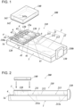
- FIG. 1 is an exploded perspective view of the light source module.
- the light source module 100 includes an optical waveguide module 110, light-emitting devices 120, a lens 130, a lid 140, and a bond layer 150 (see FIG. 3 ).
- three light-emitting devices 120 are included in the light source module 100.
- one light-emitting device 120, two light-emitting devices 120, or four or more light-emitting devices 120 may be included in the light source module 100.
- the optical waveguide module 110 includes a substrate 1, an optical waveguide 2, and a conductor layer 3.
- electrodes 4 are also included in the optical waveguide module 110.
- the substrate 1 has a first surface 1a.
- the first surface 1a in the present embodiment is greater than any other surfaces of the substrate 1.
- the substrate 1 in the present embodiment is plate-like in shape, and the first surface 1a of the substrate 1 is rectangular.
- the first surface 1a is square or has any other polygonal shape.
- the optical waveguide 2 is disposed on the first surface 1a of the substrate 1.
- the optical waveguide 2 includes a core 21 and a cladding layer 22.
- the core 21 extends in a first direction.
- the first direction is parallel to the first surface 1a. In the present embodiment, the first direction coincides with the longitudinal direction of the substrate 1.
- the core 21 When viewed obliquely, the core 21 extends from the upper left to the lower right in FIG. 1 .
- Examples of the material of the core 21 include glass (e.g., quartz) and resin.
- the core 21 in the present embodiment includes branch paths 211, a wave combining section 212, and an integration path 213.
- the branch paths 211 extend from the respective entrance surfaces to the wave combining section 212.
- the entrance surfaces are denoted by 211a (see FIG. 2 ).
- Each of the entrance surface 211a lies on a side of the corresponding one of the light-emitting devices 120.
- the branch paths 211 merge into one in the wave combining section 212.
- the integration path 213 extends from the wave combining section 212 to an exit surface 213a (see FIG. 2 ).
- the exit surface 213a in the present embodiment lies on the lens 130.
- the cladding layer 22 is disposed on the first surface 1a of the substrate 1 and extends over and around the core 21. That is, the core 21 is embedded in the cladding layer 22.
- the cladding layer 22 extends from a first end 110a to a second end 110b, where the lens 130 is located.
- Examples of the material of the cladding layer 22 include glass (e.g., quartz) and resin.
- the refractive index of the cladding layer 22 is lower than that of the core 21.
- FIG. 1 An example of the cladding layer 22 in the present embodiment is illustrated in FIG. 1 , in which a region being part of the first surface 1a and including the first end 110a opposite the second end 110b is not covered with the cladding layer 22; that is, an end portion including the first end 110a is exposed at the first surface 1a.
- the cladding layer 22 includes cavities 22a.
- Each of the cavities 22a of the cladding layer 22 in the present embodiment is provided for the corresponding one of the light-emitting devices 120.
- the cavities 22a of the cladding layer 22 in the present embodiment are provided in an end portion close to the first end 110a.
- the outline of each of the cavities 22a viewed in a direction orthogonal to the first surface 1a is rectangular and is a size larger than the outline of a mount section 41 of each electrode 4 or the outline of each light-emitting device 120.
- each of the branch paths 211 of the core 21 lies on a wall surface being one of inner wall surfaces of the corresponding one of the cavities 22a and being on a side of the second end 110b.
- the conductor layer 3 (seal ring) is disposed on the cladding layer 22.
- the conductor layer 3 in the present embodiment is in the form of a rectangular frame, and the cavities 22a of the cladding layer 22 are located in a region enclosed with the conductor layer 3.
- the conductor layer 3 is bonded to the lid 140 with the bond layer 150 (see FIG. 3 ) therebetween.
- the electrodes 4 are disposed on the first surface 1a of the substrate 1.
- Each of the electrodes 4 are provided for the corresponding one of the light-emitting devices 120.
- the electrodes 4 each include a mount section and an extended section, which are denoted by 41 and 42, respectively.
- Each of the mount sections 41 is located on a region being part of the first surface 1a and extending in the corresponding one of the cavities 22a of the cladding layer 22.
- the extended sections 42 extend from the respective mount sections 41 to the first end 110a of the substrate 1.
- the extended sections 42 extend under the end portion of the cladding layer 22 that is closer than the other end portion of the cladding layer 22 to the first end 110a.
- each extended section 42 is exposed at the first surface 1a. More specifically, the end portion is closer than the other end portion of the extended section 42 to the first end 110a and is located on an end portion of the first surface 1a that is closer than the other end portion of the first surface 1a to the first end 110a.
- the light-emitting devices 120 are located in the respective cavities 22a of the cladding layer 22.
- Each of the light-emitting devices 120 is mounted on the mount section 41 of the corresponding one of the electrodes 4.
- the light-emitting devices 120 are electrically connected to the respective electrodes 4.
- the light-emitting devices 120 are laser diodes.
- the three light-emitting devices 120 emit red light, green light, and blue light, respectively.
- the light-emitting device that emits red light is hereinafter referred to as a red-light-emitting device 120R.
- the light-emitting device that emits green light is hereinafter referred to as a green-light-emitting device 120G.
- the light-emitting device that emits blue light is hereinafter referred to as a blue-light-emitting device 120B.
- the lens 130 is fitted to the second end 110b of the optical waveguide module 110.
- the lens 130 lies on the exit surface 213a of the integration path 213 of the core 21.
- the lid 140 may include a main body 141 and a second conductor layer 142.
- the outline of the main body 141 viewed in a direction orthogonal to the first surface 1a is rectangular and is substantially coincides with the outline of the conductor layer 3.
- the main body 141 includes a recess 141a, which is located in the midsection of a surface oriented toward the substrate 1.
- the second conductor layer 142 is located on the surface of the main body 141, that is, on the surface oriented toward the substrate 1.
- the second conductor layer 142 in the present embodiment is in the form of a rectangular frame and extends along the peripheral edge of the surface of the main body 141, that is, along the peripheral edge of the surface oriented toward the substrate 1.
- the second conductor layer 142 is bonded to the conductor layer 3 of the optical waveguide module 110, with the bond layer 150 (see FIG. 3 ) being located between the second conductor layer 142 and the conductor layer 3.
- the bond layer 150 may be obtained by hardening a bonding material.
- the bonding material may be a metallic material, such as Au or Sn, or may be a glass material.
- the bond layer 150 is in close contact with both the conductor layer 3 of the optical waveguide module 110 and with the second conductor layer 142 of the lid 140.
- the lid 140 is joined to the optical waveguide module 110 accordingly.
- the light source module 100 may be as illustrated in FIG. 2 , in which the height of each light-emitting device 120 (the distance between the first surface 1a and the surface of the light-emitting device 120 that is farther than any other surfaces of the light-emitting device 120 from the substrate 1) is less than the height of the conductor layer 3 (the distance between the first surface 1a and the surface of the conductor layer 3 that is farther than any other surfaces of the substrate 1 from the substrate 1).
- the lid 140 may be in the form of a flat plate; that is, it is not required that the recess 141a be provided in the lid 140.
- Each of the light-emitting devices 120R, 120G, and 120B emits light when a predetermined voltage is applied to the extended section 42 of the corresponding one of the electrodes 4.
- Red light, green light, and blue light emitted respectively by the light-emitting devices 120R, 120G, and 120B are incident on the respective entrance surfaces 211a and enter the respective branch paths 211.
- the refractive index of the cladding layer 22 is lower than that of the core 21.
- the light in each branch path 211 is totally reflected at an interface between the branch path 211 and the cladding layer 22.
- the light is trapped in the branch path 211 while passing through the branch path 211.
- the rays of light are then combined into one in the wave combining section 212.
- the light is then reflected frontwards while passing through the integration path 213.
- the light is eventually emitted from the exit surface 213a.
- the light emitted from the exit surface 213a passes through the lens 130 and is then radiated outwards.
- optical waveguide module 110 included in the light source module 100.
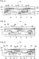
- FIG. 3 is an example of a sectional view of the optical waveguide module taken along line A-A in FIG. 1 and illustrates a state after the lid 140 is bonded to the optical waveguide module.
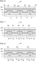
- FIGs. 4 to 8 and FIGs. 10 to 15 are other examples of the sectional view of the optical waveguide module taken long line A-A in FIG. 1 .
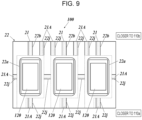
- FIG. 9 is a plan view of part of the light source module 100.
- the cladding layer 22 is disposed on the first surface 1a and extends over and around the core 21.
- the cladding layer 22 includes a protrusion 22b, which extends over the core 21 (see FIG. 3 ).
- the rest of the cladding layer 22, that is, the portion that does not extend over the core 21 is flat and is hereinafter referred to as a flat portion 22c.
- the protrusion 22b is farther than the flat portion 22c from the substrate 1.
- the protrusion 22b has a second surface 22d, which is covered with the conductor layer 3.
- the protrusion 22b includes a portion where the second surface 22d extends along the first surface 1a and is wider than the core 21.
- the second surface 22d be parallel to the first surface 1a.
- the inclination of the second surface 22d from the first surface 1a is allowed in the range of ⁇ 2°.
- the second surface 22d is the entirety of the top of the protrusion 22b viewed in section.
- FIG. 4 illustrates Variation Pattern 1, in which a corner 22e of the protrusion 22b in a sectional view taken along a line orthogonal to the first direction is curved outward.
- the corner 22e of the protrusion 22b is a place where the second surface 22d and a third surface 22f meet.
- the third surface 22f is a side extending away from the substrate 1.
- the corner 22e in Variation Pattern 1 is curved outward and away from the core 21.
- FIG. 5 illustrates Variation Pattern 2, in which the protrusion 22b includes a raised portion 22g.
- the raised portion 22g is a place where the protrusion 22b is widened toward the substrate 1.
- the third surface 22f and a fourth surface 22h meet in the raised portion 22g.
- the fourth surface 22h is a surface of the flat portion 22c and is covered with the conductor layer 3.
- part of the third surface 22f of the protrusion 22b in Variation Pattern 2 forms a slope.
- the raised portion 22g is smoothly connected to the third surface 22f and the fourth surface 22h.
- FIG. 6 illustrates Variation Pattern 3, in which the third surface 22f forms a slope where the protrusion 22b is widened toward the substrate 1.
- Adopting any of Variation Patterns 1 to 3 in the shape of the protrusion 22b enables a reduction in the thickness variance of the bond layer 150 such that stress exerted at the time of the bonding of the lid 140 to the optical waveguide module 110 is kept from concentrating in the corner 22e.
- the conductor layer 3 is impervious to being damaged.
- gaps between the protrusion 22b and the conductor layer 3 and gaps between the conductor layer 3 and the bond layer 150 are less likely be formed in the corner 22e.
- FIG. 7 illustrates Variation Pattern 4, in which the cladding layer 22 includes a recess 22i on the verge of a protruding portion of the protrusion 22b (i.e., over the boundary between the protrusion 22b and the flat portion 22c).
- the conductor layer 3 When the conductor layer 3 is caught in the recess 22i, the conductor layer 3 is less likely to come off the cladding layer 22.
- FIG. 8 illustrates Variation Pattern 5, in which the raised portion 22g of the protrusion 22b is a step.
- a region being part of the third surface 22f and located on the raised portion 22g extends along the first surface 1a and away from the core 21.
- the step 22h yields an increase in the area of contact between the protrusion 22b and the conductor layer 3. Thus, the conductor layer 3 is less likely to come off.
- FIG. 9 illustrates Variation Pattern 6, in which the cladding layer 22 includes a protrusion extending at least beside the light-emitting devices 120.
- the protrusion 22b extending over the core 21 is referred to as a first protrusion 22b
- the protrusion extending at least beside the light-emitting devices 120 is referred to as a second protrusion 22j.
- the first protrusion 22b extends in the first direction from each cavity 22a of the cladding layer 22 or, more specifically, from an end of the cavity 22a that is closer than the other end of the cavity 22a to the second end 110b.
- the second protrusion 22j preferably extends in a direction opposite the first direction from the other end of each cavity 22a, that is, from an end closer to the first end 110a than to the second end 110b.
- thermal stress exerted at the time of the bonding of the lid 140 is dispersed to a greater extent than would be possible with the first protrusion 22b only.
- the second protrusion 22j may extend parallel to the first protrusion 22b as illustrated in FIG. 9 or may extend in a direction orthogonal to the first protrusion 22b.
- the conductor layer 3 is shaped in conformance with the surface of the cladding layer 22; however, that is not necessarily the case.
- the variation patterns in the shape of the conductor layer 3 may be combined with the variation patterns in the shape of the protrusion 22b that have been described above with reference to FIGs. 4 to 8 .
- FIG. 10 illustrates Variation Pattern A, in which a region being part of the conductor layer 3 and extending over the second surface 22d of the protrusion 22b is curved outward.
- FIG. 11 illustrates Variation Pattern B, in which a region being part of the conductor layer 3 and extending over the corner 22e of the protrusion 22b is curved outward.
- FIG. 12 illustrates Variation Pattern C, in which T1 is greater than T2.
- T1 denotes the thickness of a region being part of the conductor layer 3 and extending over the corner 22e of the protrusion 22b.
- T2 denotes the thickness of a region being part of the conductor layer 3 and extending over the second surface 22d.
- FIG. 13 illustrates Variation Pattern D, in which T3 is greater than T4.
- T3 denotes the thickness of a region being part of the conductor layer 3 and extending over the verge of the protruding portion of the protrusion 22b (the boundary between the protrusion 22b and the flat portion 22c).
- T4 denotes the thickness of a region being part of the conductor layer 3 and extending over the flat portion 22c of the cladding layer 22.
- the flat portion 22c is not included in the protrusion 22b; that is, the flat portion 22c is adjacent to the raised portion 22g.
- FIG. 14 illustrates Variation Pattern E, in which a region being part of the conductor layer 3 and extending over the verge of the protruding portion of the protrusion 22b is curved outward.
- FIG. 15 illustrates Variation Pattern F, in which a region being part of the conductor layer 3 and extending over the verge of the protruding portion of the protrusion 22b is curved inward.
- the following describes a method for manufacturing the optical waveguide module 110.
- FIG. 16 is a sectional view of the optical waveguide module 110 in the process of being manufactured.
- the method for manufacturing the optical waveguide module 110 includes a first cladding layer forming step, a core forming step, a second cladding layer forming step, a smoothing step, a cavity forming step, and a conductor layer forming step.
- FIG. 16A illustrates the first cladding layer forming step, in which a first cladding layer 221 is formed on the first surface 1a of the substrate 1, with the electrodes 4 being disposed on the first surface 1a.
- the first cladding layer 221 is part of the cladding layer 22.
- the step of forming the first cladding layer 221 on the substrate 1 is followed by the core forming step.
- FIG. 16B illustrates the core forming step, in which the core 21 is formed on a surface of the first cladding layer 221.
- the details of the core forming step are as follows.
- the surface of the first cladding layer 221 is entirety covered with a core layer.
- Unwanted portions are then removed from the core layer by, for example, etching.
- the core layer left unremoved is the core 21.
- the core forming step includes forming a dummy core 21A in a region where the second protrusion 22j is to be formed.
- the core 21 and the dummy core 21A may be made of the same material or may be made of different materials.
- the degrees of thermal expansion of the core 21 and the dummy core 21A are matched. This feature eliminates or reduces the possibility that stress will concentrate in part of the cladding layer 22 due to nonuniformity in thermal expansion.
- the step of forming the core 21 is followed by the second cladding layer forming step.
- FIG. 16C illustrates the second cladding layer forming step, in which the first cladding layer 221 and the core 21 are overlaid with a second cladding layer 222.
- the second cladding layer 222 formed in this step and the first cladding layer 221 constitute the cladding layer 22.
- a region being part of the second cladding layer 222 and extending over the core 21 is the protrusion 22b.
- the second cladding layer 222 is thinner than it used to be. To that end, the manufacturing method in the present embodiment involves forming the second cladding layer 222 over an extended period of time or at a higher speed. Consequently, the second surface 22d of the protrusion 22b becomes wider than the core 21.
- the step of forming the second cladding layer 222 is followed by the smoothing step.
- FIG. 16D illustrates the smoothing step, in which the entire surface of the protrusion 22b (including the second surface 22d, the third surface 22f, and the corner 22e and the raised portion 22g of the protrusion 22b) is smoothed.
- the entire surface of the cladding layer 22 including the protrusion 22b is subjected to blasting or wet etching.
- This process is easier than removing the protrusion 22b by polishing.
- the protrusion 22b is cut into a desired shape when undergoing the smoothing step.
- the step of forming the second cladding layer 222 or the step of smoothing the entire surface of the protrusion 22b is followed by the cavity forming step.
- the cavities 22a are formed in part of the cladding layer 22, which includes the first cladding layer 221 and the second cladding layer 222 stacked on the first cladding layer 221.
- the step of forming the cavities 22a in the cladding layer 22 is followed by the conductor layer forming step.
- FIG. 16E illustrates the conductor layer forming step, in which the conductor layer 3 is formed on the second surface 22d of the cladding layer 22 in such a manner that the cavities 22a are located in a region enclosed with the conductor layer 3.
- the conductor layer 3 is formed by, for example, plating or sputtering.
- the conductor layer forming step involves, for example, adjustment of the direction in which metal atoms are ejected from a sputtering target.
- the optical waveguide module 110 according to the present embodiment has been described so far.
- the optical waveguide module 110 and the light source module 100 including the optical waveguide module 110 can be manufactured without the need to remove the protrusion.
- the present embodiment reduces the possibility that thermal stress caused by heat of the bonding material will concentrate in the protrusion 22b.
- the present embodiment saves time and effort in manufacturing the light source module 100.
- the protrusion 22b and the conductor layer 3 are impervious to being damage during the bonding of the lid 140.
- the light source module 100 thus has high reliability and is long-wearing.
- the present embodiment reduces the thermal stress exerted on the protrusion 22b and thus eliminates or reduces the possibility of deformation of the core 21 and the possibility of displacement of the optical axis.
- the optical waveguide module 110 and the light source module 100 according to the present embodiment can operate without deterioration in light transmission efficiency.
- the present disclosure is applicable to optical waveguide modules and light source modules.
Landscapes
- Physics & Mathematics (AREA)
- General Physics & Mathematics (AREA)
- Optics & Photonics (AREA)
- Engineering & Computer Science (AREA)
- Microelectronics & Electronic Packaging (AREA)
- Optical Integrated Circuits (AREA)
- Optical Couplings Of Light Guides (AREA)
Abstract
Description
- The present disclosure relates to an optical waveguide module and a light source module.
- A known optical waveguide module includes a substrate, a core, a cladding layer, and a conductor layer. The core extends in a predetermined direction. The cladding layer is disposed on the substrate and extends over and around the core. The conductor layer is disposed on the cladding layer.
- In an example of the known optical waveguide module, a region being part of a surface of the cladding layer and extending over the core is flat (see, for example, Patent Literature 1).
- In another example of the known optical waveguide module, the cladding layer includes a protrusion extending over the core (see, for example, Patent Literature 2).
-
- Patent Literature 1:
Japanese Patent No. 4579868 - Patent Literature 2:
Japanese Unexamined Patent Application Publication No. 10-308555 - According to an aspect of the present disclosure, an optical waveguide module includes a substrate, a core, a cladding layer, and a conductor layer. The substrate has a first surface. The core extends in a first direction. The cladding layer is disposed on the first surface and extends over and around the core. The conductor layer is disposed on the cladding layer. The cladding layer includes a protrusion extending over the core. The protrusion has a second surface covered with the conductor layer and includes a portion where the second surface extends along the first surface and is wider than the core.
- According to an aspect of the position of the present disclosure, a light source module includes the optical waveguide module, an electrode, a light-emitting element, and a lid. The electrode is disposed on a first surface of the optical waveguide module. The light-emitting device is disposed on the electrode. The light-emitting device is covered with the lid.
-
-
FIG. 1 is an exploded perspective view of a light source module according to an embodiment of the present disclosure. -
FIG. 2 is a side view of the light source module according to another embodiment of the present disclosure. -
FIGs. 3 to 8 are examples of a sectional view taken along line A-A inFIG. 1 . -
FIG. 9 is a plan view of part of the light source module according to the another embodiment. -
FIGs. 10 to 15 are other examples of the sectional view taken along line A-A inFIG. 1 . -
FIGs. 16A to 16E are sectional views of an optical waveguide module in the process of being manufactured, where the optical waveguide module is to be included in the light source module illustrated inFIG. 1 . - The manufacturing of the module described in
Patent Literature 1 involves the step of removing (e.g., by polishing) a protrusion from a cladding layer formed on a core in the preceding step. The removal of the protrusion developed over the core has been a burden in manufacturing the module described inPatent Literature 1. - The manufacturing of the module described in
Patent Literature 2 does not involve the step of removing such a protrusion. On the downside, heat generated by a bonding material during the bonding of a lid to the module causes concentration of thermal stress in the protrusion. The thermal stress can cause damage to the protrusion and/or a conductor layer. More specifically, the protrusion can be cracked, and/or the conductor layer can come off the protrusion. - This problem is averted by an optical waveguide module disclosed herein; that is, the protrusion and the conductor layer are impervious to being damage during the bonding of the lid. The optical waveguide module thus has high reliability and is long-wearing.
- A light source module disclosed herein also has high reliability.
- Hereinafter, an embodiment of the present disclosure will be described in detail with reference to the accompanying drawings.
- The embodiment and examples illustrated in the drawings should not be construed as limiting the technical scope of the present disclosure.
- The following describes the configuration of a
light source module 100 according to an embodiment of the present disclosure. -
FIG. 1 is an exploded perspective view of the light source module. - Referring to
FIG. 1 , thelight source module 100 includes anoptical waveguide module 110, light-emitting devices 120, alens 130, alid 140, and a bond layer 150 (seeFIG. 3 ). - In the present embodiment, three light-
emitting devices 120 are included in thelight source module 100. - In some embodiments, one light-
emitting device 120, two light-emitting devices 120, or four or more light-emittingdevices 120 may be included in thelight source module 100. - The
optical waveguide module 110 includes asubstrate 1, anoptical waveguide 2, and aconductor layer 3. - In the present embodiment,
electrodes 4 are also included in theoptical waveguide module 110. - The
substrate 1 has a first surface 1a. - The first surface 1a in the present embodiment is greater than any other surfaces of the
substrate 1. - The
substrate 1 in the present embodiment is plate-like in shape, and the first surface 1a of thesubstrate 1 is rectangular. - In some embodiments, the first surface 1a is square or has any other polygonal shape.
- The
optical waveguide 2 is disposed on the first surface 1a of thesubstrate 1. - The
optical waveguide 2 includes acore 21 and acladding layer 22. - The
core 21 extends in a first direction. - The first direction is parallel to the first surface 1a. In the present embodiment, the first direction coincides with the longitudinal direction of the
substrate 1. - When viewed obliquely, the
core 21 extends from the upper left to the lower right inFIG. 1 . - Examples of the material of the core 21 include glass (e.g., quartz) and resin.
- The core 21 in the present embodiment includes
branch paths 211, awave combining section 212, and anintegration path 213. - The
branch paths 211 extend from the respective entrance surfaces to thewave combining section 212. The entrance surfaces are denoted by 211a (seeFIG. 2 ). - Each of the
entrance surface 211a lies on a side of the corresponding one of the light-emittingdevices 120. - The
branch paths 211 merge into one in thewave combining section 212. - The
integration path 213 extends from thewave combining section 212 to anexit surface 213a (seeFIG. 2 ). - The
exit surface 213a in the present embodiment lies on thelens 130. - The
cladding layer 22 is disposed on the first surface 1a of thesubstrate 1 and extends over and around thecore 21. That is, thecore 21 is embedded in thecladding layer 22. - The
cladding layer 22 extends from afirst end 110a to asecond end 110b, where thelens 130 is located. - Examples of the material of the
cladding layer 22 include glass (e.g., quartz) and resin. - The refractive index of the
cladding layer 22 is lower than that of thecore 21. - An example of the
cladding layer 22 in the present embodiment is illustrated inFIG. 1 , in which a region being part of the first surface 1a and including thefirst end 110a opposite thesecond end 110b is not covered with thecladding layer 22; that is, an end portion including thefirst end 110a is exposed at the first surface 1a. - The
cladding layer 22 includescavities 22a. - Each of the
cavities 22a of thecladding layer 22 in the present embodiment is provided for the corresponding one of the light-emittingdevices 120. - The
cavities 22a of thecladding layer 22 in the present embodiment are provided in an end portion close to thefirst end 110a. - In the present embodiment, the outline of each of the
cavities 22a viewed in a direction orthogonal to the first surface 1a is rectangular and is a size larger than the outline of amount section 41 of eachelectrode 4 or the outline of each light-emittingdevice 120. - The
entrance surface 211a of each of thebranch paths 211 of the core 21 lies on a wall surface being one of inner wall surfaces of the corresponding one of thecavities 22a and being on a side of thesecond end 110b. - The conductor layer 3 (seal ring) is disposed on the
cladding layer 22. - The
conductor layer 3 in the present embodiment is in the form of a rectangular frame, and thecavities 22a of thecladding layer 22 are located in a region enclosed with theconductor layer 3. - The
conductor layer 3 is bonded to thelid 140 with the bond layer 150 (seeFIG. 3 ) therebetween. - The
electrodes 4 are disposed on the first surface 1a of thesubstrate 1. - Each of the
electrodes 4 are provided for the corresponding one of the light-emittingdevices 120. - The
electrodes 4 each include a mount section and an extended section, which are denoted by 41 and 42, respectively. - Each of the
mount sections 41 is located on a region being part of the first surface 1a and extending in the corresponding one of thecavities 22a of thecladding layer 22. - The
extended sections 42 extend from therespective mount sections 41 to thefirst end 110a of thesubstrate 1. Theextended sections 42 extend under the end portion of thecladding layer 22 that is closer than the other end portion of thecladding layer 22 to thefirst end 110a. - An end portion of each
extended section 42 is exposed at the first surface 1a. More specifically, the end portion is closer than the other end portion of theextended section 42 to thefirst end 110a and is located on an end portion of the first surface 1a that is closer than the other end portion of the first surface 1a to thefirst end 110a. - The light-emitting
devices 120 are located in therespective cavities 22a of thecladding layer 22. - Each of the light-emitting
devices 120 is mounted on themount section 41 of the corresponding one of theelectrodes 4. The light-emittingdevices 120 are electrically connected to therespective electrodes 4. - For example, the light-emitting
devices 120 are laser diodes. - The three light-emitting
devices 120 emit red light, green light, and blue light, respectively. The light-emitting device that emits red light is hereinafter referred to as a red-light-emitting device 120R. The light-emitting device that emits green light is hereinafter referred to as a green-light-emitting device 120G. The light-emitting device that emits blue light is hereinafter referred to as a blue-light-emitting device 120B. - The
lens 130 is fitted to thesecond end 110b of theoptical waveguide module 110. - The
lens 130 lies on theexit surface 213a of theintegration path 213 of thecore 21. - The
lid 140 may include amain body 141 and asecond conductor layer 142. - The outline of the
main body 141 viewed in a direction orthogonal to the first surface 1a is rectangular and is substantially coincides with the outline of theconductor layer 3. - The
main body 141 includes arecess 141a, which is located in the midsection of a surface oriented toward thesubstrate 1. - The
second conductor layer 142 is located on the surface of themain body 141, that is, on the surface oriented toward thesubstrate 1. - The
second conductor layer 142 in the present embodiment is in the form of a rectangular frame and extends along the peripheral edge of the surface of themain body 141, that is, along the peripheral edge of the surface oriented toward thesubstrate 1. - The
second conductor layer 142 is bonded to theconductor layer 3 of theoptical waveguide module 110, with the bond layer 150 (seeFIG. 3 ) being located between thesecond conductor layer 142 and theconductor layer 3. - The
bond layer 150 may be obtained by hardening a bonding material. - The bonding material may be a metallic material, such as Au or Sn, or may be a glass material.
- The
bond layer 150 is in close contact with both theconductor layer 3 of theoptical waveguide module 110 and with thesecond conductor layer 142 of thelid 140. Thelid 140 is joined to theoptical waveguide module 110 accordingly. - The
light source module 100 may be as illustrated inFIG. 2 , in which the height of each light-emitting device 120 (the distance between the first surface 1a and the surface of the light-emittingdevice 120 that is farther than any other surfaces of the light-emittingdevice 120 from the substrate 1) is less than the height of the conductor layer 3 (the distance between the first surface 1a and the surface of theconductor layer 3 that is farther than any other surfaces of thesubstrate 1 from the substrate 1). - In this case, the
lid 140 may be in the form of a flat plate; that is, it is not required that therecess 141a be provided in thelid 140. - Each of the light-emitting devices 120R, 120G, and 120B emits light when a predetermined voltage is applied to the
extended section 42 of the corresponding one of theelectrodes 4. - Red light, green light, and blue light emitted respectively by the light-emitting devices 120R, 120G, and 120B are incident on the
respective entrance surfaces 211a and enter therespective branch paths 211. - As mentioned above, the refractive index of the
cladding layer 22 is lower than that of thecore 21. The light in eachbranch path 211 is totally reflected at an interface between thebranch path 211 and thecladding layer 22. Thus, the light is trapped in thebranch path 211 while passing through thebranch path 211. - The rays of light are then combined into one in the
wave combining section 212. - The light is then reflected frontwards while passing through the
integration path 213. The light is eventually emitted from theexit surface 213a. - The light emitted from the
exit surface 213a passes through thelens 130 and is then radiated outwards. - The following describes features of the
optical waveguide module 110 included in thelight source module 100. -
FIG. 3 is an example of a sectional view of the optical waveguide module taken along line A-A inFIG. 1 and illustrates a state after thelid 140 is bonded to the optical waveguide module.FIGs. 4 to 8 andFIGs. 10 to 15 are other examples of the sectional view of the optical waveguide module taken long line A-A inFIG. 1 .FIG. 9 is a plan view of part of thelight source module 100. - As mentioned above, the
cladding layer 22 is disposed on the first surface 1a and extends over and around thecore 21. - The
cladding layer 22 includes aprotrusion 22b, which extends over the core 21 (seeFIG. 3 ). - The rest of the
cladding layer 22, that is, the portion that does not extend over thecore 21 is flat and is hereinafter referred to as aflat portion 22c. - The
protrusion 22b is farther than theflat portion 22c from thesubstrate 1. - The
protrusion 22b has asecond surface 22d, which is covered with theconductor layer 3. Theprotrusion 22b includes a portion where thesecond surface 22d extends along the first surface 1a and is wider than thecore 21. - It is not always required that the
second surface 22d be parallel to the first surface 1a. The inclination of thesecond surface 22d from the first surface 1a is allowed in the range of ±2°. - Referring to
FIG. 3 , thesecond surface 22d is the entirety of the top of theprotrusion 22b viewed in section. - There are variation patterns in the shape of the
protrusion 22b viewed in section. - The variation patterns will be described below one by one.
-
FIG. 4 illustratesVariation Pattern 1, in which acorner 22e of theprotrusion 22b in a sectional view taken along a line orthogonal to the first direction is curved outward. - The
corner 22e of theprotrusion 22b is a place where thesecond surface 22d and athird surface 22f meet. Thethird surface 22f is a side extending away from thesubstrate 1. - The
corner 22e inVariation Pattern 1 is curved outward and away from thecore 21. -
FIG. 5 illustratesVariation Pattern 2, in which theprotrusion 22b includes a raisedportion 22g. The raisedportion 22g is a place where theprotrusion 22b is widened toward thesubstrate 1. - The
third surface 22f and afourth surface 22h meet in the raisedportion 22g. Thefourth surface 22h is a surface of theflat portion 22c and is covered with theconductor layer 3. - In other words, part of the
third surface 22f of theprotrusion 22b inVariation Pattern 2 forms a slope. - In the present embodiment, the raised
portion 22g is smoothly connected to thethird surface 22f and thefourth surface 22h. -
FIG. 6 illustratesVariation Pattern 3, in which thethird surface 22f forms a slope where theprotrusion 22b is widened toward thesubstrate 1. - In other words, the entirety of the
third surface 22f of theprotrusion 22b inVariation Pattern 3 forms a slope. - Adopting any of
Variation Patterns 1 to 3 in the shape of theprotrusion 22b enables a reduction in the thickness variance of thebond layer 150 such that stress exerted at the time of the bonding of thelid 140 to theoptical waveguide module 110 is kept from concentrating in thecorner 22e. - Thus, the
conductor layer 3 is impervious to being damaged. - In addition to that, gaps between the
protrusion 22b and theconductor layer 3 and gaps between theconductor layer 3 and thebond layer 150 are less likely be formed in thecorner 22e. -
FIG. 7 illustratesVariation Pattern 4, in which thecladding layer 22 includes arecess 22i on the verge of a protruding portion of theprotrusion 22b (i.e., over the boundary between theprotrusion 22b and theflat portion 22c). - In
Variation Pattern 4, theconductor layer 3 is caught in therecess 22i. - When the
conductor layer 3 is caught in therecess 22i, theconductor layer 3 is less likely to come off thecladding layer 22. -
FIG. 8 illustrates Variation Pattern 5, in which the raisedportion 22g of theprotrusion 22b is a step. - More specifically, a region being part of the
third surface 22f and located on the raisedportion 22g extends along the first surface 1a and away from thecore 21. - The
step 22h yields an increase in the area of contact between theprotrusion 22b and theconductor layer 3. Thus, theconductor layer 3 is less likely to come off. -
FIG. 9 illustrates Variation Pattern 6, in which thecladding layer 22 includes a protrusion extending at least beside the light-emittingdevices 120. To make protrusions distinguishable from each other, theprotrusion 22b extending over thecore 21 is referred to as afirst protrusion 22b, and the protrusion extending at least beside the light-emittingdevices 120 is referred to as asecond protrusion 22j. - The
first protrusion 22b extends in the first direction from eachcavity 22a of thecladding layer 22 or, more specifically, from an end of thecavity 22a that is closer than the other end of thecavity 22a to thesecond end 110b. Meanwhile, thesecond protrusion 22j preferably extends in a direction opposite the first direction from the other end of eachcavity 22a, that is, from an end closer to thefirst end 110a than to thesecond end 110b. - Owing to this feature, thermal stress exerted at the time of the bonding of the
lid 140 is dispersed to a greater extent than would be possible with thefirst protrusion 22b only. - The
second protrusion 22j may extend parallel to thefirst protrusion 22b as illustrated inFIG. 9 or may extend in a direction orthogonal to thefirst protrusion 22b. - Referring to
FIGs. 3 to 8 , theconductor layer 3 is shaped in conformance with the surface of thecladding layer 22; however, that is not necessarily the case. - There are variation patterns in the shape of the
conductor layer 3 viewed in plan. - The variation patterns will be described below one by one.
- Although the following describes examples in which the shape of the
protrusion 22b viewed in section is analogous to the shape illustrated inFIG. 3 , the variation patterns in the shape of theconductor layer 3 may be combined with the variation patterns in the shape of theprotrusion 22b that have been described above with reference toFIGs. 4 to 8 . -
FIG. 10 illustrates Variation Pattern A, in which a region being part of theconductor layer 3 and extending over thesecond surface 22d of theprotrusion 22b is curved outward. -
FIG. 11 illustrates Variation Pattern B, in which a region being part of theconductor layer 3 and extending over thecorner 22e of theprotrusion 22b is curved outward. -
FIG. 12 illustrates Variation Pattern C, in which T1 is greater than T2. T1 denotes the thickness of a region being part of theconductor layer 3 and extending over thecorner 22e of theprotrusion 22b. T2 denotes the thickness of a region being part of theconductor layer 3 and extending over thesecond surface 22d. -
FIG. 13 illustrates Variation Pattern D, in which T3 is greater than T4. T3 denotes the thickness of a region being part of theconductor layer 3 and extending over the verge of the protruding portion of theprotrusion 22b (the boundary between theprotrusion 22b and theflat portion 22c). T4 denotes the thickness of a region being part of theconductor layer 3 and extending over theflat portion 22c of thecladding layer 22. Theflat portion 22c is not included in theprotrusion 22b; that is, theflat portion 22c is adjacent to the raisedportion 22g. -
FIG. 14 illustrates Variation Pattern E, in which a region being part of theconductor layer 3 and extending over the verge of the protruding portion of theprotrusion 22b is curved outward. -
FIG. 15 illustrates Variation Pattern F, in which a region being part of theconductor layer 3 and extending over the verge of the protruding portion of theprotrusion 22b is curved inward. - The following describes a method for manufacturing the
optical waveguide module 110. -
FIG. 16 is a sectional view of theoptical waveguide module 110 in the process of being manufactured. - The method for manufacturing the
optical waveguide module 110 according to the present embodiment includes a first cladding layer forming step, a core forming step, a second cladding layer forming step, a smoothing step, a cavity forming step, and a conductor layer forming step. -
FIG. 16A illustrates the first cladding layer forming step, in which afirst cladding layer 221 is formed on the first surface 1a of thesubstrate 1, with theelectrodes 4 being disposed on the first surface 1a. Thefirst cladding layer 221 is part of thecladding layer 22. - The step of forming the
first cladding layer 221 on thesubstrate 1 is followed by the core forming step. -
FIG. 16B illustrates the core forming step, in which thecore 21 is formed on a surface of thefirst cladding layer 221. - The details of the core forming step are as follows. The surface of the
first cladding layer 221 is entirety covered with a core layer. - Unwanted portions are then removed from the core layer by, for example, etching.
- The core layer left unremoved is the
core 21. - In a case in which the
second protrusion 22j is to be provided in theoptical waveguide module 110, the core forming step includes forming adummy core 21A in a region where thesecond protrusion 22j is to be formed. - This facilitates forming the
second protrusion 22j in the second cladding layer forming step, which will be described later. - The
core 21 and thedummy core 21A may be made of the same material or may be made of different materials. - When the
core 21 and thedummy core 21A are made of the same material, the degrees of thermal expansion of thecore 21 and thedummy core 21A are matched. This feature eliminates or reduces the possibility that stress will concentrate in part of thecladding layer 22 due to nonuniformity in thermal expansion. - The step of forming the
core 21 is followed by the second cladding layer forming step. -
FIG. 16C illustrates the second cladding layer forming step, in which thefirst cladding layer 221 and the core 21 are overlaid with asecond cladding layer 222. - The
second cladding layer 222 formed in this step and thefirst cladding layer 221 constitute thecladding layer 22. - A region being part of the
second cladding layer 222 and extending over thecore 21 is theprotrusion 22b. - The
second cladding layer 222 is thinner than it used to be. To that end, the manufacturing method in the present embodiment involves forming thesecond cladding layer 222 over an extended period of time or at a higher speed. Consequently, thesecond surface 22d of theprotrusion 22b becomes wider than thecore 21. - The step of forming the
second cladding layer 222 is followed by the smoothing step. -
FIG. 16D illustrates the smoothing step, in which the entire surface of theprotrusion 22b (including thesecond surface 22d, thethird surface 22f, and thecorner 22e and the raisedportion 22g of theprotrusion 22b) is smoothed. - More specifically, the entire surface of the
cladding layer 22 including theprotrusion 22b is subjected to blasting or wet etching. - This process is easier than removing the
protrusion 22b by polishing. - In a case in which any of the variation patterns is adopted to the shape of the
protrusion 22b viewed in section, theprotrusion 22b is cut into a desired shape when undergoing the smoothing step. - The step of forming the
second cladding layer 222 or the step of smoothing the entire surface of theprotrusion 22b is followed by the cavity forming step. - In the cavity forming step, the
cavities 22a (seeFIG. 1 ) are formed in part of thecladding layer 22, which includes thefirst cladding layer 221 and thesecond cladding layer 222 stacked on thefirst cladding layer 221. - The step of forming the
cavities 22a in thecladding layer 22 is followed by the conductor layer forming step. -
FIG. 16E illustrates the conductor layer forming step, in which theconductor layer 3 is formed on thesecond surface 22d of thecladding layer 22 in such a manner that thecavities 22a are located in a region enclosed with theconductor layer 3. - More specifically, the
conductor layer 3 is formed by, for example, plating or sputtering. - In a case in which any of the variation patterns is adopted to the shape of the
conductor layer 3 viewed in section, the conductor layer forming step involves, for example, adjustment of the direction in which metal atoms are ejected from a sputtering target. - This is how the
optical waveguide module 110 is manufactured. - The
optical waveguide module 110 according to the present embodiment has been described so far. Theoptical waveguide module 110 and thelight source module 100 including theoptical waveguide module 110 can be manufactured without the need to remove the protrusion. - Where the
optical waveguide module 110 and thelight source module 100 are concerned, the present embodiment reduces the possibility that thermal stress caused by heat of the bonding material will concentrate in theprotrusion 22b. - The present embodiment saves time and effort in manufacturing the
light source module 100. Theprotrusion 22b and theconductor layer 3 are impervious to being damage during the bonding of thelid 140. Thelight source module 100 thus has high reliability and is long-wearing. - Where the
optical waveguide module 110 and thelight source module 100 are concerned, the present embodiment reduces the thermal stress exerted on theprotrusion 22b and thus eliminates or reduces the possibility of deformation of thecore 21 and the possibility of displacement of the optical axis. Thus, theoptical waveguide module 110 and thelight source module 100 according to the present embodiment can operate without deterioration in light transmission efficiency. - The present disclosure is applicable to optical waveguide modules and light source modules.
-
- 100
- light source module
110 optical waveguide module
1 substrate
1a first surface
2 optical waveguide
21 core
211 branch path
211a entrance surface
212 wave combining section
213 integration path
213a exit surface
21A dummy core
22 cladding layer
22a cavity
22b protrusion (first protrusion)
22c flat portion
22d second surface
22e corner
22f third surface
22g raised portion
22h fourth surface
22i recess
22j second protrusion
221 first cladding layer
222 second cladding layer
3 conductor layer
4 electrode
41 mount section
42 extended section
120 light-emitting device
120B blue-light-emitting device
120G green-light-emitting device
120R red-light-emitting device
130 lens
140 lid
141 main body
141a recess
142 second conductor layer
150 bond layer
Claims (16)
- An optical waveguide module, comprising:a substrate having a first surface;a core extending in a first direction;a cladding layer disposed on the first surface and extending over and around the core; anda conductor layer disposed on the cladding layer, whereinthe cladding layer comprises a protrusion extending over the core, andthe protrusion has a second surface in contact with the conductor layer and comprises a portion where the second surface extends along the first surface and is wider than the core.
- The optical waveguide module according to claim 1, wherein the protrusion comprises a corner curved outward in a sectional view taken along a line orthogonal to the first direction.
- The optical waveguide module according to claim 1, wherein the protrusion comprises a raised portion where the protrusion is widened toward the substrate.
- The optical waveguide module according to claim 1, wherein the protrusion has a third surface connected to the second surface and forming a slope where the protrusion is widened toward the substrate.
- The optical waveguide module according to any one of claims 1 to 4, wherein the cladding layer comprises a recess on a verge of a protruding portion of the protrusion.
- The optical waveguide module according to claim 1, wherein the protrusion comprises a raised portion being a step protruding away from the core.
- The optical waveguide module according to any one of claims 1 to 6, wherein the conductor layer is shaped in conformance with a surface of the cladding layer.
- The optical waveguide module according to any one of claims 1 to 6, wherein a region being part of the conductor layer and extending over the second surface of the protrusion is curved outward.
- The optical waveguide module according to any one of claims 1 to 6, wherein a region being part of the conductor layer and extending over a corner of the protrusion is curved outward.
- The optical waveguide module according to any one of claims 1 to 6, wherein a region being part of the conductor layer and extending over a corner of the protrusion is thicker than a region being part of the conductor layer and extending over the second surface.
- The optical waveguide module according to any one of claims 1 to 6, wherein a region being part of the conductor layer and extending over a verge of a protruding portion of the protrusion is thicker than a region being part of the conductor layer and extending over a portion of the cladding layer, wherein the portion is not included in the protrusion.
- The optical waveguide module according to any one of claims 1 to 6, wherein a region being part of the conductor layer and extending over a verge of a protruding portion of the protrusion is curved outward.
- The optical waveguide module according to any one of claims 1 to 6, wherein a region being part of the conductor layer and extending over a verge of a protruding portion of the protrusion is curved inward.
- The optical waveguide module according to any one of claims 1 to 13, whereinthe core is an optical waveguide through which light emitted by a light-emitting device passes, andthe cladding layer comprises a second protrusion extending at least beside the light-emitting device, wherein the protrusion extending over the core is a first protrusion.
- A light source module, comprising:the optical waveguide module according to any one of claims 1 to 14;an electrode disposed on a first surface of the optical waveguide module;a light-emitting device disposed on the electrode; anda lid covering the light-emitting device.
- The light source module according to claim 15, wherein the light source module comprises a plurality of the light-emitting devices comprising a red-light-emitting device, a green-light-emitting device, and a blue-light-emitting device.
Applications Claiming Priority (2)
| Application Number | Priority Date | Filing Date | Title |
|---|---|---|---|
| JP2020062409 | 2020-03-31 | ||
| PCT/JP2021/012066 WO2021200408A1 (en) | 2020-03-31 | 2021-03-23 | Optical waveguide module and light source module |
Publications (2)
| Publication Number | Publication Date |
|---|---|
| EP4130821A1 true EP4130821A1 (en) | 2023-02-08 |
| EP4130821A4 EP4130821A4 (en) | 2024-04-24 |
Family
ID=77928621
Family Applications (1)
| Application Number | Title | Priority Date | Filing Date |
|---|---|---|---|
| EP21778792.8A Pending EP4130821A4 (en) | 2020-03-31 | 2021-03-23 | Optical waveguide module and light source module |
Country Status (5)
| Country | Link |
|---|---|
| US (1) | US20230168449A1 (en) |
| EP (1) | EP4130821A4 (en) |
| JP (1) | JP7480277B2 (en) |
| CN (1) | CN115380232B (en) |
| WO (1) | WO2021200408A1 (en) |
Families Citing this family (2)
| Publication number | Priority date | Publication date | Assignee | Title |
|---|---|---|---|---|
| CN118647912A (en) * | 2022-02-10 | 2024-09-13 | 京瓷株式会社 | Optical waveguide substrate, optical waveguide package, and light source module |
| WO2024162456A1 (en) * | 2023-02-02 | 2024-08-08 | 京セラ株式会社 | Optoelectric wiring board |
Family Cites Families (22)
| Publication number | Priority date | Publication date | Assignee | Title |
|---|---|---|---|---|
| JP2862625B2 (en) * | 1990-03-16 | 1999-03-03 | 日本電信電話株式会社 | Embedded quartz optical waveguide and method of manufacturing the same |
| JPH10308555A (en) * | 1997-05-01 | 1998-11-17 | Nippon Telegr & Teleph Corp <Ntt> | Hybrid waveguide type optical circuit and manufacturing method thereof |
| US6343171B1 (en) * | 1998-10-09 | 2002-01-29 | Fujitsu Limited | Systems based on opto-electronic substrates with electrical and optical interconnections and methods for making |
| US6393185B1 (en) * | 1999-11-03 | 2002-05-21 | Sparkolor Corporation | Differential waveguide pair |
| US6981806B2 (en) * | 2002-07-05 | 2006-01-03 | Xponent Photonics Inc | Micro-hermetic packaging of optical devices |
| US6985646B2 (en) * | 2003-01-24 | 2006-01-10 | Xponent Photonics Inc | Etched-facet semiconductor optical component with integrated end-coupled waveguide and methods of fabrication and use thereof |
| JP2005148468A (en) * | 2003-11-17 | 2005-06-09 | Sony Corp | Optical waveguide, light source module, and optical information processing apparatus |
| KR20070012631A (en) | 2003-12-05 | 2007-01-26 | 유니버시티 오브 피츠버그 오브 더 커먼웰쓰 시스템 오브 하이어 에듀케이션 | Metallic nano-optical lenses and beam shaping devices |
| US7184640B2 (en) * | 2004-02-25 | 2007-02-27 | Avago Technologies Fiber Ip (Singapore) Pte. Ltd. | Buried heterostructure device fabricated by single step MOCVD |
| JP2006058858A (en) * | 2004-07-22 | 2006-03-02 | Nippon Telegr & Teleph Corp <Ntt> | Waveguide-type thermo-optic phase shifter and its optical circuit |
| JP2006208518A (en) * | 2005-01-26 | 2006-08-10 | Seikoh Giken Co Ltd | Thermo-optical effect type optical waveguide element and its manufacturing method |
| GB0511300D0 (en) * | 2005-06-03 | 2005-07-13 | Ct For Integrated Photonics Th | Control of vertical axis for passive alignment of optical components with wave guides |
| JP4579868B2 (en) | 2006-06-08 | 2010-11-10 | 日本電信電話株式会社 | Optical integrated circuit |
| JP5195700B2 (en) * | 2009-09-18 | 2013-05-08 | 富士通株式会社 | Optical semiconductor device and manufacturing method thereof |
| WO2012002975A1 (en) * | 2010-07-02 | 2012-01-05 | Hewlett-Packard Development Company, L.P. | Optical splitter array |
| JP6090655B2 (en) * | 2013-02-12 | 2017-03-08 | パナソニックIpマネジメント株式会社 | Dry film for optical waveguide, optical waveguide and photoelectric composite wiring board using the same, and method for producing optical composite wiring board |
| JP2015064413A (en) * | 2013-09-24 | 2015-04-09 | 富士通株式会社 | Optical semiconductor element and manufacturing method therefor |
| CN103698847B (en) * | 2013-12-27 | 2016-01-20 | 南京邮电大学 | A kind of matching strengthens the method for long chain molecule type polymer optical wave guide birefringence |
| JP6691518B2 (en) * | 2017-08-17 | 2020-04-28 | 日本電信電話株式会社 | Optical integrated circuit |
| US10641824B2 (en) * | 2017-11-19 | 2020-05-05 | Emcore Corporation | Electrically conductive metal film for a semiconductor device |
| JP2019125738A (en) * | 2018-01-18 | 2019-07-25 | シャープ株式会社 | Semiconductor laser element, method of manufacturing the same, and light-emitting device |
| JP7060798B2 (en) * | 2018-05-30 | 2022-04-27 | 日亜化学工業株式会社 | Light source device |
-
2021
- 2021-03-23 WO PCT/JP2021/012066 patent/WO2021200408A1/en not_active Ceased
- 2021-03-23 EP EP21778792.8A patent/EP4130821A4/en active Pending
- 2021-03-23 JP JP2022511991A patent/JP7480277B2/en active Active
- 2021-03-23 US US17/915,811 patent/US20230168449A1/en active Pending
- 2021-03-23 CN CN202180024647.6A patent/CN115380232B/en active Active
Also Published As
| Publication number | Publication date |
|---|---|
| EP4130821A4 (en) | 2024-04-24 |
| WO2021200408A1 (en) | 2021-10-07 |
| CN115380232A (en) | 2022-11-22 |
| US20230168449A1 (en) | 2023-06-01 |
| JP7480277B2 (en) | 2024-05-09 |
| JPWO2021200408A1 (en) | 2021-10-07 |
| CN115380232B (en) | 2025-06-20 |
Similar Documents
| Publication | Publication Date | Title |
|---|---|---|
| CN105103314B (en) | Semiconductor device and method for manufacturing semiconductor device | |
| EP4130821A1 (en) | Optical waveguide module and light source module | |
| JPWO2018180952A1 (en) | Nitride semiconductor light emitting device, method of manufacturing nitride semiconductor light emitting device, and nitride semiconductor light emitting device | |
| CN105210202A (en) | Light-emitting semiconductor component and method for producing light-emitting semiconductor components | |
| US20190207071A1 (en) | Radiation-emitting component | |
| JP2017216423A (en) | Semiconductor light emitting device and manufacturing method thereof | |
| JP2009064961A (en) | Semiconductor laser device and manufacturing method thereof | |
| CN101960683A (en) | Semiconductor laser element and manufacturing method thereof | |
| JP2009123939A (en) | Nitride-based semiconductor element and manufacturing method therefor | |
| CN114077016A (en) | Package structure with photonic integrated circuit | |
| JP7736696B2 (en) | Semiconductor light emitting device and light source device | |
| US20160056614A1 (en) | Semiconductor laser diode with shortened cavity length | |
| KR20170106347A (en) | Method for producing a plurality of optoelectronic semiconductor components and optoelectronic semiconductor component | |
| US11929590B2 (en) | Method for producing optical semiconductor device | |
| JP2000106352A (en) | Method of manufacturing laser fusing semiconductor device and semiconductor device | |
| US12345913B2 (en) | Optical waveguide package and light source module | |
| JP2012243960A (en) | Semiconductor laser device | |
| TW202320364A (en) | light emitting device | |
| TW202340772A (en) | Optical waveguide substrate, optical waveguide package and light source module | |
| JPWO2023233525A5 (en) | ||
| US8422522B2 (en) | Semiconductor laser device | |
| TWI873424B (en) | Light source module | |
| JP2021162660A (en) | Optical waveguide module and light source module | |
| JP7068560B1 (en) | Manufacturing method of semiconductor laser device and semiconductor laser device | |
| EP4485024A1 (en) | Optical waveguide substrate, optical waveguide package, and light source module |
Legal Events
| Date | Code | Title | Description |
|---|---|---|---|
| STAA | Information on the status of an ep patent application or granted ep patent |
Free format text: STATUS: THE INTERNATIONAL PUBLICATION HAS BEEN MADE |
|
| PUAI | Public reference made under article 153(3) epc to a published international application that has entered the european phase |
Free format text: ORIGINAL CODE: 0009012 |
|
| STAA | Information on the status of an ep patent application or granted ep patent |
Free format text: STATUS: REQUEST FOR EXAMINATION WAS MADE |
|
| 17P | Request for examination filed |
Effective date: 20220927 |
|
| AK | Designated contracting states |
Kind code of ref document: A1 Designated state(s): AL AT BE BG CH CY CZ DE DK EE ES FI FR GB GR HR HU IE IS IT LI LT LU LV MC MK MT NL NO PL PT RO RS SE SI SK SM TR |
|
| P01 | Opt-out of the competence of the unified patent court (upc) registered |
Effective date: 20230505 |
|
| DAV | Request for validation of the european patent (deleted) | ||
| DAX | Request for extension of the european patent (deleted) | ||
| A4 | Supplementary search report drawn up and despatched |
Effective date: 20240321 |
|
| RIC1 | Information provided on ipc code assigned before grant |
Ipc: G02B 6/132 20060101ALI20240315BHEP Ipc: G02B 6/43 20060101ALI20240315BHEP Ipc: G02B 6/122 20060101ALI20240315BHEP Ipc: G02B 6/42 20060101ALI20240315BHEP Ipc: G02B 6/13 20060101ALI20240315BHEP Ipc: G02B 6/12 20060101AFI20240315BHEP |