EP4125261A1 - Electronic device - Google Patents
Electronic device Download PDFInfo
- Publication number
- EP4125261A1 EP4125261A1 EP22153952.1A EP22153952A EP4125261A1 EP 4125261 A1 EP4125261 A1 EP 4125261A1 EP 22153952 A EP22153952 A EP 22153952A EP 4125261 A1 EP4125261 A1 EP 4125261A1
- Authority
- EP
- European Patent Office
- Prior art keywords
- light
- light guiding
- electronic device
- sub
- infrared transmitter
- Prior art date
- Legal status (The legal status is an assumption and is not a legal conclusion. Google has not performed a legal analysis and makes no representation as to the accuracy of the status listed.)
- Granted
Links
Images


Classifications
-
- H—ELECTRICITY
- H04—ELECTRIC COMMUNICATION TECHNIQUE
- H04M—TELEPHONIC COMMUNICATION
- H04M1/00—Substation equipment, e.g. for use by subscribers
- H04M1/02—Constructional features of telephone sets
- H04M1/0202—Portable telephone sets, e.g. cordless phones, mobile phones or bar type handsets
- H04M1/026—Details of the structure or mounting of specific components
-
- G—PHYSICS
- G01—MEASURING; TESTING
- G01J—MEASUREMENT OF INTENSITY, VELOCITY, SPECTRAL CONTENT, POLARISATION, PHASE OR PULSE CHARACTERISTICS OF INFRARED, VISIBLE OR ULTRAVIOLET LIGHT; COLORIMETRY; RADIATION PYROMETRY
- G01J1/00—Photometry, e.g. photographic exposure meter
- G01J1/42—Photometry, e.g. photographic exposure meter using electric radiation detectors
- G01J1/4204—Photometry, e.g. photographic exposure meter using electric radiation detectors with determination of ambient light
-
- G—PHYSICS
- G01—MEASURING; TESTING
- G01J—MEASUREMENT OF INTENSITY, VELOCITY, SPECTRAL CONTENT, POLARISATION, PHASE OR PULSE CHARACTERISTICS OF INFRARED, VISIBLE OR ULTRAVIOLET LIGHT; COLORIMETRY; RADIATION PYROMETRY
- G01J1/00—Photometry, e.g. photographic exposure meter
- G01J1/02—Details
- G01J1/04—Optical or mechanical part supplementary adjustable parts
- G01J1/0407—Optical elements not provided otherwise, e.g. manifolds, windows, holograms, gratings
-
- H—ELECTRICITY
- H04—ELECTRIC COMMUNICATION TECHNIQUE
- H04M—TELEPHONIC COMMUNICATION
- H04M1/00—Substation equipment, e.g. for use by subscribers
- H04M1/02—Constructional features of telephone sets
- H04M1/0202—Portable telephone sets, e.g. cordless phones, mobile phones or bar type handsets
- H04M1/026—Details of the structure or mounting of specific components
- H04M1/0266—Details of the structure or mounting of specific components for a display module assembly
-
- H—ELECTRICITY
- H04—ELECTRIC COMMUNICATION TECHNIQUE
- H04M—TELEPHONIC COMMUNICATION
- H04M2250/00—Details of telephonic subscriber devices
- H04M2250/12—Details of telephonic subscriber devices including a sensor for measuring a physical value, e.g. temperature or motion
Definitions
- An ambient light sensor configured in an electronic device can sense the external ambient light intensity, so the display brightness of the electronic device can be adjusted. Moreover, when the quantity of the ambient light sensors configured in the electronic device increases, the detection range of an ambient light field can be greatly increased to reflect the ambient light situation around a mobile phone more truly. How to increase the quantity of the ambient light sensors and optimize the layout space of the electronic device simultaneously has become a technical problem to be solved.
- the disclosure relates to the technical field of terminals, and to an electronic device, to solve deficiencies in the related art.
- an electronic device includes:
- the light incident end is arranged facing the light-transmitting area, and the light emitting end is arranged facing the ambient light sensor and the infrared transmitter.
- first, second, etc. may be used in the disclosure to describe various information, the information should not be limited to these terms. These terms are only used to distinguish the same type of information from each other.
- first information may also be referred to as second information, and similarly, the second information may also be referred to as first information.
- Fig. 1 is a schematic structural diagram of an electronic device 100 shown according to an example.
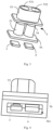
- Fig. 2 is a schematic structural diagram of a light guiding piece 5 shown according to an example.
- Fig. 3 is an exploded view chart of the light guiding piece 5 in Fig. 2 .
- the electronic device 100 may include a housing 1 or shell, a display panel 2, an ambient light sensor 3, an infrared transmitter 4 and a light guiding piece 5.
- the housing 1 may include a battery cover, a middle frame or a front shell.
- the display panel 2 may be connected with the front shell of the electronic device 100, so as to display an image through the display panel 2 which may include a light-transmitting area 21.
- the ambient light sensor 3, the infrared transmitter 4 and the light guiding piece 5 may all be arranged in the electronic device 100.
- the ambient light sensor 3 and the infrared transmitter 4 may be connected to the housing 1 or other components in the electronic device 100, and/or the ambient light sensor 3 and/or the infrared transmitter 4 may also be connected and fixed to the light guiding piece 5.
- the external ambient light intensity of the electronic device 100 can be sensed through the ambient light sensor 3, and then the electronic device 100 can adjust the brightness of the display panel 2 according to the ambient light intensity.
- the infrared transmitter 4 can emit infrared light towards the outside of the electronic device 100, for example, a remote control or ranging function of the electronic device 100 can be achieved through the infrared light.
- the light guiding piece 5 may include a light incident end 51 and a light emitting end 52.
- the light incident end 51 is configured facing the light-transmitting area 21 of the display panel 2
- the light emitting end 52 may be configured facing the ambient light sensor 3 and the infrared transmitter 4, so that the external ambient light can be transmitted to the ambient light sensor through the light-transmitting area 21 and the light guiding piece 5, while the infrared light emitted by the infrared transmitter 4 can also be emitted to the outside of the electronic device 100 through the light guiding piece 5 and the light-transmitting area 21. Based on this, the ambient light and the infrared light can be transmitted simultaneously through the light guiding piece 5.
- the ambient light sensor 3 and the infrared transmitter 4 can share the same light guiding piece 5, which is conducive to increasing the quantity of the ambient light sensors 3 for the electronic device 100, so as to improve the detection accuracy of the ambient light intensity, and further save the internal space of the electronic device.
- the above description takes the display panel 2 including the light-transmitting area 21 as an example.
- the light-transmitting area may also be formed on the housing 1, for example, an opening may be processed and formed in the housing 1 as the light-transmitting area, or an opening may be formed in a top of the housing 1 as the light-transmitting area.
- the display area of the display panel 2 does not need to be occupied in the solution where the light-transmitting area is formed on the housing 1, and the light-transmitting area may not be arranged on a display side of the electronic device 100, which can improve the visual effect. And when the light-transmitting area is located at the top of the electronic device 100, it is conducive to increasing the light field range of the ambient light sensor 3 and greatly improving the detection accuracy.
- the ambient light sensor 3 and the infrared transmitter 4 can guide light through different light guiding channels of the light guiding piece 5 respectively.
- the light guiding piece 5 may include a first light guiding column 53, a second light guiding column 54 and a light-shielding body 55.
- the light-shielding body 55 may include a first mounting hole 551 and a second mounting hole 552.
- the first light guiding column 53 may be arranged in the first mounting hole 551, in which a first end of the first light guiding column 53 is configured facing the light-transmitting area 21, and a second end of the first light guiding column 53 is configured facing the ambient light sensor 3.
- the second light guiding column 54 may be arranged in the second mounting hole 552, in which a first end of the second light guiding column 54 may be configured facing the light-transmitting area 21, and a second end of the second light guiding column 54 may be configured facing the infrared transmitter 4. Based on this, an infrared light path of the infrared transmitter 4 and an ambient light path of the ambient light sensor 3 can be physically isolated to avoid light crosstalk and affecting the detection accuracy of the ambient light sensor 3.
- the light-shielding body 55 may include a non-light-transmitting polycarbonate light-shielding body, and external light is prevented from being emitted through sides of the first light guiding column 53 and the second light guiding column 54.
- the first light guiding column 53 may include a light-transmitting acrylic light guiding column
- the second light guiding column 54 may include a light-transmitting acrylic light guiding column.
- the light guiding piece 5 may further include a light guiding seat body 56, which is respectively connected with the first light guiding column 53, the second light guiding column 54 and the light-shielding body 55.
- the light guiding seat body 56 may further be connected with the housing 1 of the electronic device 100, so as to fix the light guiding piece 5 into the electronic device 100 and avoid moving.
- the ambient light sensor 3 and the infrared transmitter 4 may be connected to an end, facing away from the first light guiding column 53 and the second light guiding column 54, of the light guiding seat body 56, so as to achieve the purpose of light guidance through the first light guiding column 53 and the second light guiding column 54.
- the first light guiding column 53, the second light guiding column 54 and the light guiding seat body 56 may be integrally formed, or in other cases, the first light guiding column 53, the second light guiding column 54 and the light guiding seat body 56 may also be separately formed, and their relative position relationship may be fixed by bonding or other means.
- the light guiding seat body 56 and the light-shielding body 55 may be fixedly connected by bonding.
- the light guiding seat body 56 may include a mounting groove 561 recessed from a side facing away from the light-shielding body 55, and the ambient light sensor 3 and the infrared transmitter 4 may both be located in the mounting groove 561, so that light can be converged by the surrounding effect of the mounting groove 561.
- the loss of the light can be reduced, and it is conducive to improving the detection accuracy of the ambient light sensor 3 and the remote control effectiveness of the infrared transmitter 4.
- the light guiding piece 5 may include a shared part 57, a first light guiding sub-part 58 and a second light guiding sub-part 59.
- the first light guiding sub-part 58 and the second light guiding sub-part 59 are connected to a first end of the shared part 57, from which the first light guiding sub-part 58 and the second light guiding sub-part 59 extend in different directions respectively.
- An end, away from the shared part 57, of the first light guiding sub-part 58 is configured facing the ambient light sensor 3, and an end, away from the shared part 57, of the second light guiding sub-part 59 is configured facing the infrared transmitter 4, so that the ambient light can be transmitted through the first light guiding sub-part 58, and the infrared light can be transmitted through the second light guiding sub-part 59.
- An end, away from the first light guiding sub-part 58 and the second light guiding sub-part 59, of the shared part 57 is configured facing the light-transmitting area 21.
- the shared part 57 may include a light-shielding boundary layer 571 including a first edge and two opposing second edge.
- the first edge is located between the first light guiding sub-part 58 and the second light guiding sub-part 59, and the second edge extends in the height direction of the shared part 57 until to be at least flush with a surface of the shared part 57.
- the shared part 57 may be divided into two parts through the light-shielding boundary layer 571, so that one part may be connected with the first light guiding sub-part 58, and the other part may be connected with the second light guiding sub-part 59, so as to achieve the light path isolation of the ambient light and the infrared light on the shared part 57.
- the shared part 57 includes a polycarbonate light-transmitting shared part.
- the first light guiding sub-part 58 may include a visible light guiding sub-part
- the second light guiding sub-part 59 may include an infrared light guiding sub-part.
- a sectional area of the first light guiding sub-part 58 may decrease progressively from an end close to the shared part 57 to an end away from the shared part 57.
- the second light guiding sub-part 59 may include an arc-shaped surface 591, which is located on a side, away from the first light guiding sub-part 58, of the second light guiding sub-part 59.
- An emission direction of the infrared transmitter 4 points to the arc-shaped surface 591 from an end, away from the shared part 57, of the second light guiding sub-part 59, so that the infrared transmitter 4 may emit the infrared light towards the arc-shaped surface 591 of the second light guiding sub-part 59. Since the arc-shaped surface 591 can increase the area of a reflecting surface, more infrared light can be reflected, which is conducive to reducing the loss of the infrared light.
- the ambient light sensor 3 and the infrared transmitter 4 may also share the same light guiding channel of the light guiding piece 5, so as to simplify a structure of the light guiding piece 5.
- the light guiding piece 5 may be an integrated light guiding column which may transmit infrared light and visible light.
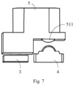
- the integrated light guiding column includes a first lens part 510 and a second lens part 511 which are arranged on the light emitting end 52.
- the first lens part 510 faces the ambient light sensor 3, and the second lens part 511 faces the infrared transmitter 4. Based on this, the loss of light can be reduced by using the condensing effect of the first lens part 510 and the second lens part 511.
- an end, facing the ambient light sensor 3 and the infrared transmitter 4, of the integrated light guiding column may be basically at the same height.
- the height difference between the first lens part 510 and the second lens part 511 may be greater than zero, so as to adapt to the ambient light sensor 3 and the infrared transmitter 4, which is conducive to the layout of other components in the electronic device 100.
Landscapes
- Physics & Mathematics (AREA)
- General Physics & Mathematics (AREA)
- Spectroscopy & Molecular Physics (AREA)
- Life Sciences & Earth Sciences (AREA)
- Sustainable Development (AREA)
- Engineering & Computer Science (AREA)
- Signal Processing (AREA)
- Photometry And Measurement Of Optical Pulse Characteristics (AREA)
Abstract
Description
- An ambient light sensor configured in an electronic device can sense the external ambient light intensity, so the display brightness of the electronic device can be adjusted. Moreover, when the quantity of the ambient light sensors configured in the electronic device increases, the detection range of an ambient light field can be greatly increased to reflect the ambient light situation around a mobile phone more truly. How to increase the quantity of the ambient light sensors and optimize the layout space of the electronic device simultaneously has become a technical problem to be solved.
- The disclosure relates to the technical field of terminals, and to an electronic device, to solve deficiencies in the related art.
- According to an example of the disclosure, an electronic device is provided and includes:
- a housing;
- a display panel connected to the housing, the display panel or the housing including a light-transmitting area;
- an ambient light sensor arranged in the housing;
- an infrared transmitter arranged in the housing; and
- a light guiding piece including a light incident end and a light emitting end.
- The light incident end is arranged facing the light-transmitting area, and the light emitting end is arranged facing the ambient light sensor and the infrared transmitter.
- The drawings herein are incorporated into the specification and constitute a part of the specification, which show examples consistent with the disclosure, and are used together with the specification to explain the principle of the disclosure.
-
Fig. 1 is a schematic structural diagram of an electronic device shown according to an example. -
Fig. 2 is a schematic structural diagram of a light guiding piece shown according to an example. -
Fig. 3 is an exploded view chart of the light guiding piece inFig. 2 . -
Fig. 4 is a schematic structural diagram of another light guiding piece shown according to an example. -
Fig. 5 is a schematic structural diagram of another light guiding piece shown according to an example. -
Fig. 6 is a schematic structural diagram of another light guiding piece shown according to an example. -
Fig. 7 is a schematic structural diagram of another light guiding piece shown according to an example. - Examples will be described in detail herein, implementations of which are illustrated in the accompanying drawings. When the following description refers to the accompanying drawings, the same numbers in different drawings represent the same or similar elements unless otherwise indicated. The implementation manners described in the following examples do not represent all implementation manners consistent with the disclosure. On the contrary, they are merely examples of an apparatus or a method consistent with some aspects of the disclosure as detailed.
- The terms used in the disclosure are only for the purpose of describing specific examples, and are not intended to limit the disclosure. The singular forms of "a", "an", and "the" used in the disclosure are also intended to include plural forms, unless the context clearly indicates other meanings.
- It should be understood that although the terms "first", "second", etc. may be used in the disclosure to describe various information, the information should not be limited to these terms. These terms are only used to distinguish the same type of information from each other. For example, without departing from the scope of the disclosure, the first information may also be referred to as second information, and similarly, the second information may also be referred to as first information.
-
Fig. 1 is a schematic structural diagram of anelectronic device 100 shown according to an example.Fig. 2 is a schematic structural diagram of a light guidingpiece 5 shown according to an example.Fig. 3 is an exploded view chart of the light guidingpiece 5 inFig. 2 . As shown inFig. 1 to Fig. 3 , theelectronic device 100 may include ahousing 1 or shell, adisplay panel 2, anambient light sensor 3, aninfrared transmitter 4 and a light guidingpiece 5. Thehousing 1 may include a battery cover, a middle frame or a front shell. Thedisplay panel 2 may be connected with the front shell of theelectronic device 100, so as to display an image through thedisplay panel 2 which may include a light-transmittingarea 21. Theambient light sensor 3, theinfrared transmitter 4 and the light guidingpiece 5 may all be arranged in theelectronic device 100. For example, theambient light sensor 3 and theinfrared transmitter 4 may be connected to thehousing 1 or other components in theelectronic device 100, and/or theambient light sensor 3 and/or theinfrared transmitter 4 may also be connected and fixed to the light guidingpiece 5. The external ambient light intensity of theelectronic device 100 can be sensed through theambient light sensor 3, and then theelectronic device 100 can adjust the brightness of thedisplay panel 2 according to the ambient light intensity. Theinfrared transmitter 4 can emit infrared light towards the outside of theelectronic device 100, for example, a remote control or ranging function of theelectronic device 100 can be achieved through the infrared light. - The light guiding
piece 5 may include alight incident end 51 and alight emitting end 52. Thelight incident end 51 is configured facing the light-transmittingarea 21 of thedisplay panel 2, and thelight emitting end 52 may be configured facing theambient light sensor 3 and theinfrared transmitter 4, so that the external ambient light can be transmitted to the ambient light sensor through the light-transmittingarea 21 and the light guidingpiece 5, while the infrared light emitted by theinfrared transmitter 4 can also be emitted to the outside of theelectronic device 100 through the light guidingpiece 5 and the light-transmittingarea 21. Based on this, the ambient light and the infrared light can be transmitted simultaneously through the light guidingpiece 5. Theambient light sensor 3 and theinfrared transmitter 4 can share the samelight guiding piece 5, which is conducive to increasing the quantity of theambient light sensors 3 for theelectronic device 100, so as to improve the detection accuracy of the ambient light intensity, and further save the internal space of the electronic device. The above description takes thedisplay panel 2 including the light-transmittingarea 21 as an example. In fact, in other examples, the light-transmitting area may also be formed on thehousing 1, for example, an opening may be processed and formed in thehousing 1 as the light-transmitting area, or an opening may be formed in a top of thehousing 1 as the light-transmitting area. Compared with the solution of forming the light-transmittingarea 21 on thedisplay panel 2, the display area of thedisplay panel 2 does not need to be occupied in the solution where the light-transmitting area is formed on thehousing 1, and the light-transmitting area may not be arranged on a display side of theelectronic device 100, which can improve the visual effect. And when the light-transmitting area is located at the top of theelectronic device 100, it is conducive to increasing the light field range of theambient light sensor 3 and greatly improving the detection accuracy. - In the example, the
ambient light sensor 3 and theinfrared transmitter 4 can guide light through different light guiding channels of the light guidingpiece 5 respectively. In one example, as still shown inFig. 2 andFig. 3 , the light guidingpiece 5 may include a firstlight guiding column 53, a secondlight guiding column 54 and a light-shielding body 55. The light-shielding body 55 may include afirst mounting hole 551 and asecond mounting hole 552. The firstlight guiding column 53 may be arranged in thefirst mounting hole 551, in which a first end of the firstlight guiding column 53 is configured facing the light-transmittingarea 21, and a second end of the firstlight guiding column 53 is configured facing theambient light sensor 3. The secondlight guiding column 54 may be arranged in thesecond mounting hole 552, in which a first end of the secondlight guiding column 54 may be configured facing the light-transmittingarea 21, and a second end of the secondlight guiding column 54 may be configured facing theinfrared transmitter 4. Based on this, an infrared light path of theinfrared transmitter 4 and an ambient light path of theambient light sensor 3 can be physically isolated to avoid light crosstalk and affecting the detection accuracy of theambient light sensor 3. The light-shieldingbody 55 may include a non-light-transmitting polycarbonate light-shielding body, and external light is prevented from being emitted through sides of the firstlight guiding column 53 and the secondlight guiding column 54. The firstlight guiding column 53 may include a light-transmitting acrylic light guiding column, and the secondlight guiding column 54 may include a light-transmitting acrylic light guiding column. - Further, the light guiding
piece 5 may further include a light guidingseat body 56, which is respectively connected with the firstlight guiding column 53, the secondlight guiding column 54 and the light-shielding body 55. The light guidingseat body 56 may further be connected with thehousing 1 of theelectronic device 100, so as to fix the light guidingpiece 5 into theelectronic device 100 and avoid moving. Theambient light sensor 3 and theinfrared transmitter 4 may be connected to an end, facing away from the firstlight guiding column 53 and the secondlight guiding column 54, of the light guidingseat body 56, so as to achieve the purpose of light guidance through the firstlight guiding column 53 and the secondlight guiding column 54. The firstlight guiding column 53, the secondlight guiding column 54 and the light guidingseat body 56 may be integrally formed, or in other cases, the firstlight guiding column 53, the secondlight guiding column 54 and the light guidingseat body 56 may also be separately formed, and their relative position relationship may be fixed by bonding or other means. The light guidingseat body 56 and the light-shieldingbody 55 may be fixedly connected by bonding. - In the example, as shown in
Fig. 4 , the light guidingseat body 56 may include amounting groove 561 recessed from a side facing away from the light-shielding body 55, and theambient light sensor 3 and theinfrared transmitter 4 may both be located in themounting groove 561, so that light can be converged by the surrounding effect of themounting groove 561. Thus, compared with the solution that the light guidingseat body 56 is spaced from theambient light sensor 3 and theinfrared transmitter 4, the loss of the light can be reduced, and it is conducive to improving the detection accuracy of theambient light sensor 3 and the remote control effectiveness of theinfrared transmitter 4. - In another example, as shown in
Fig. 5 , thelight guiding piece 5 may include a sharedpart 57, a firstlight guiding sub-part 58 and a secondlight guiding sub-part 59. The firstlight guiding sub-part 58 and the secondlight guiding sub-part 59 are connected to a first end of the sharedpart 57, from which the firstlight guiding sub-part 58 and the secondlight guiding sub-part 59 extend in different directions respectively. An end, away from the sharedpart 57, of the firstlight guiding sub-part 58 is configured facing the ambientlight sensor 3, and an end, away from the sharedpart 57, of the secondlight guiding sub-part 59 is configured facing theinfrared transmitter 4, so that the ambient light can be transmitted through the firstlight guiding sub-part 58, and the infrared light can be transmitted through the secondlight guiding sub-part 59. An end, away from the firstlight guiding sub-part 58 and the secondlight guiding sub-part 59, of the sharedpart 57 is configured facing the light-transmittingarea 21. In order to achieve the physical isolation of the ambient light path and the infrared light path on the sharedpart 57, the sharedpart 57 may include a light-shieldingboundary layer 571 including a first edge and two opposing second edge. The first edge is located between the firstlight guiding sub-part 58 and the secondlight guiding sub-part 59, and the second edge extends in the height direction of the sharedpart 57 until to be at least flush with a surface of the sharedpart 57. Based on this, the sharedpart 57 may be divided into two parts through the light-shieldingboundary layer 571, so that one part may be connected with the firstlight guiding sub-part 58, and the other part may be connected with the secondlight guiding sub-part 59, so as to achieve the light path isolation of the ambient light and the infrared light on the sharedpart 57. The sharedpart 57 includes a polycarbonate light-transmitting shared part. One part, connected with the firstlight guiding sub-part 58 and located on a side of the light-shieldingboundary layer 571, of the polycarbonate light-transmitting shared part may transmit the ambient light; and one part, connected with the secondlight guiding sub-part 59 and located on a side of the light-shieldingboundary layer 571, of the polycarbonate light-transmitting shared part may transmit the infrared light. The firstlight guiding sub-part 58 may include a visible light guiding sub-part, and the secondlight guiding sub-part 59 may include an infrared light guiding sub-part. - Further, as still shown in
Fig. 5 , a sectional area of the firstlight guiding sub-part 58 may decrease progressively from an end close to the sharedpart 57 to an end away from the sharedpart 57. In other words, the closer the end of the firstlight guiding sub-part 58 is to the ambientlight sensor 3, the smaller the sectional area is, so as to facilitate the convergence of the ambient light irradiated from the outside. The secondlight guiding sub-part 59 may include an arc-shapedsurface 591, which is located on a side, away from the firstlight guiding sub-part 58, of the secondlight guiding sub-part 59. An emission direction of theinfrared transmitter 4 points to the arc-shapedsurface 591 from an end, away from the sharedpart 57, of the secondlight guiding sub-part 59, so that theinfrared transmitter 4 may emit the infrared light towards the arc-shapedsurface 591 of the secondlight guiding sub-part 59. Since the arc-shapedsurface 591 can increase the area of a reflecting surface, more infrared light can be reflected, which is conducive to reducing the loss of the infrared light. - In other cases, the ambient
light sensor 3 and theinfrared transmitter 4 may also share the same light guiding channel of thelight guiding piece 5, so as to simplify a structure of thelight guiding piece 5. For example, as shown inFig. 6 , thelight guiding piece 5 may be an integrated light guiding column which may transmit infrared light and visible light. The integrated light guiding column includes afirst lens part 510 and asecond lens part 511 which are arranged on thelight emitting end 52. Thefirst lens part 510 faces the ambientlight sensor 3, and thesecond lens part 511 faces theinfrared transmitter 4. Based on this, the loss of light can be reduced by using the condensing effect of thefirst lens part 510 and thesecond lens part 511. In the example, when the ambientlight sensor 3 and theinfrared transmitter 4 are located at the same height, as shown inFig. 6 , an end, facing the ambientlight sensor 3 and theinfrared transmitter 4, of the integrated light guiding column may be basically at the same height. When an end, facing thelight guiding piece 5, of the ambientlight sensor 3 and an end, facing thelight guiding piece 5, of theinfrared transmitter 4 are located at different heights, as shown inFig. 7 , in a height direction of the integrated light guiding column, the height difference between thefirst lens part 510 and thesecond lens part 511 may be greater than zero, so as to adapt to the ambientlight sensor 3 and theinfrared transmitter 4, which is conducive to the layout of other components in theelectronic device 100. - After considering the specification and practicing the disclosure disclosed herein, those skilled in the art will easily think of other embodiments of the disclosure. The disclosure is intended to cover any variations, uses, or adaptive changes of the disclosure. These variations, uses, or adaptive changes follow the general principles of the disclosure and include common knowledge or conventional technical means in the technical field that are not disclosed in the disclosure.
- It will be appreciated that the disclosure is not limited to the exact construction that has been described above and illustrated in the accompanying drawings, and that various modifications and changes can be made without departing from the scope thereof. It is intended that the scope of the disclosure only be limited by the appended claims.
Claims (15)
- An electronic device, comprising:a housing (1);a display panel (2) connected to the housing (1), wherein the display panel (2) or the housing (1) comprises a light-transmitting area (21);an ambient light sensor (3) arranged in the housing (1);an infrared transmitter (4) arranged in the housing (1); anda light guiding piece (5) comprising a light incident end (51) and a light emitting end (52), wherein the light incident end (51) is configured facing the light-transmitting area (21), and the light emitting end (52) is configured facing the ambient light sensor (3) and the infrared transmitter (4).
- The electronic device of claim 1, wherein the ambient light sensor (3) and the infrared transmitter (4) share one same light guiding channel of the light guiding piece (5); or
the ambient light sensor (3) and the infrared transmitter (4) respectively correspond to different light guiding channels of the light guiding piece (5). - The electronic device according to claim 1, wherein the light guiding piece (5) comprises:a light-shielding body (55) comprising a first mounting hole (551) and a second mounting hole (552);a first light guiding column (53) arranged in the first mounting hole (551), wherein a first end of the first light guiding column (53) is configured facing the ambient light sensor (3), and a second end of the first light guiding column (53) is configured facing the transparent area (21); anda second light guiding column (54) arranged in the second mounting hole (552), wherein a first end of the second light guiding column (54) is configured facing the infrared transmitter (4), and a second end of the second light guiding column (54) is configured facing the transparent area (21).
- The electronic device according to claim 3, wherein the light guiding piece (5) further comprises a light guiding seat body (56) connected with the housing (1), wherein the light guiding seat body (56) is respectively connected with the first light guiding column (53), the second light guiding column (54) and the light-shielding body (55), and the ambient light sensor (3) and the infrared transmitter (4) are located on a side, facing away from the first light guiding column (53) and the second light guiding column (54), of the light guiding seat body (56).
- The electronic device according to any of claims 3 or 4, wherein the light guiding seat body (56) comprises a mounting groove (561) recessed from a side facing away from the light-shielding body (55), and the ambient light sensor (3) and the infrared transmitter (4) are located in the mounting groove (561).
- The electronic device according to any of claims 3 to 5, wherein the light-shielding body (55) comprises a non-light-transmitting polycarbonate light-shielding body.
- The electronic device according to any of claims 3 to 6, wherein the first light guiding column (53) and the second light guiding column (54) respectively comprise a light-transmitting acrylic light guiding column.
- The electronic device according to claim 1, wherein the light guiding piece (5) comprises a shared part (57), a first light guiding sub-part (58) and a second light guiding sub-part (59),wherein the first light guiding sub-part (58) and the second light guiding sub-part (59) are connected to a first end of the shared part (57) and extend in different directions, and a second end of the shared part (57) is configured facing the light-transmitting area (21),wherein an ambient light path and an infrared light path on the shared part (57) are physically isolated, andwherein the first light guiding sub-part (58) is configured facing the ambient light sensor (3), and the second light guiding sub-part (59) is configured facing the infrared transmitter (4).
- The electronic device according to claim 8, wherein the shared part (57) comprises a light-shielding boundary layer (571) comprising a first edge and two opposing second edges, wherein the first edge is located between the first light guiding sub-part (58) and the second light guiding sub-part (59), and the second edge extends in a height direction of the shared part (57) until to be at least flush with a surface of the shared part (57).
- The electronic device according to claim 8 or 9, wherein a sectional area of the first light guiding sub-part (58) decreases progressively from an end close to the shared part (57) to an end away from the shared part (57).
- The electronic device according to any of claims 8 to 10, wherein the second light guiding sub-part () comprises an arc-shaped surface (591) located on a side, away from the first light guiding sub-part (58), of the second light guiding sub-part (59), and an emission direction of the infrared transmitter (4) points to the arc-shaped surface (591) from an end, away from the shared part (57), of the second light guiding sub-part (59).
- The electronic device according to any of claims 8 to 11, wherein the shared part (57) comprises a polycarbonate light-transmitting shared part.
- The electronic device according to any of claims 8 to 12, wherein the first light guiding sub-part (58) comprises a visible light guiding sub-part, and the second light guiding sub-part (59) comprises an infrared light guiding sub-part.
- The electronic device according to claim 1, wherein the light guiding piece () comprises an integrated light guiding column capable of transmitting infrared light and visible light, wherein the integrated light guiding column comprises:a first lens part (510) arranged on the light emitting end (51), wherein the first lens part (510) faces the ambient light sensor (3), anda second lens part (511) arranged on the light emitting end (51), wherein the second lens part (511) faces the infrared transmitter (4).
- The electronic device according to claim 14, wherein in a height direction of the integrated light guiding column, a height difference between the first lens part (510) and the second lens part (511) is greater than zero; or
an end, facing the ambient light sensor (3) and the infrared transmitter (4), of the integrated light guiding column is at the same height.
Applications Claiming Priority (1)
| Application Number | Priority Date | Filing Date | Title |
|---|---|---|---|
| CN202110857353.3A CN115695598A (en) | 2021-07-28 | 2021-07-28 | Electronic equipment |
Publications (2)
| Publication Number | Publication Date |
|---|---|
| EP4125261A1 true EP4125261A1 (en) | 2023-02-01 |
| EP4125261B1 EP4125261B1 (en) | 2025-07-23 |
Family
ID=80122733
Family Applications (1)
| Application Number | Title | Priority Date | Filing Date |
|---|---|---|---|
| EP22153952.1A Active EP4125261B1 (en) | 2021-07-28 | 2022-01-28 | Electronic device |
Country Status (3)
| Country | Link |
|---|---|
| US (1) | US11768105B2 (en) |
| EP (1) | EP4125261B1 (en) |
| CN (1) | CN115695598A (en) |
Citations (4)
| Publication number | Priority date | Publication date | Assignee | Title |
|---|---|---|---|---|
| CN208924284U (en) * | 2018-09-12 | 2019-05-31 | Oppo广东移动通信有限公司 | A kind of sensor module and electronic device |
| CN109120752B (en) * | 2018-08-21 | 2020-05-08 | Oppo广东移动通信有限公司 | Electronic device |
| US20210136189A1 (en) * | 2018-07-16 | 2021-05-06 | Guangdong Oppo Mobile Telecommunications Corp., Ltd. | Electronic device and front shell thereof |
| US20210181402A1 (en) * | 2018-08-30 | 2021-06-17 | Japan Display Inc. | Electronic device |
Family Cites Families (2)
| Publication number | Priority date | Publication date | Assignee | Title |
|---|---|---|---|---|
| US11436964B1 (en) * | 2018-11-13 | 2022-09-06 | Apple Inc. | Electronic devices having image transport layers and electrical components |
| US11289051B2 (en) * | 2020-08-24 | 2022-03-29 | Apple Inc. | Electronic devices having light sensor modules overlapped by displays |
-
2021
- 2021-07-28 CN CN202110857353.3A patent/CN115695598A/en active Pending
-
2022
- 2022-01-27 US US17/585,895 patent/US11768105B2/en active Active
- 2022-01-28 EP EP22153952.1A patent/EP4125261B1/en active Active
Patent Citations (4)
| Publication number | Priority date | Publication date | Assignee | Title |
|---|---|---|---|---|
| US20210136189A1 (en) * | 2018-07-16 | 2021-05-06 | Guangdong Oppo Mobile Telecommunications Corp., Ltd. | Electronic device and front shell thereof |
| CN109120752B (en) * | 2018-08-21 | 2020-05-08 | Oppo广东移动通信有限公司 | Electronic device |
| US20210181402A1 (en) * | 2018-08-30 | 2021-06-17 | Japan Display Inc. | Electronic device |
| CN208924284U (en) * | 2018-09-12 | 2019-05-31 | Oppo广东移动通信有限公司 | A kind of sensor module and electronic device |
Also Published As
| Publication number | Publication date |
|---|---|
| US11768105B2 (en) | 2023-09-26 |
| CN115695598A (en) | 2023-02-03 |
| US20230032527A1 (en) | 2023-02-02 |
| EP4125261B1 (en) | 2025-07-23 |
Similar Documents
| Publication | Publication Date | Title |
|---|---|---|
| EP3694192B1 (en) | Electronic device with display screen, infrared sensor and light sensor | |
| EP3716253B1 (en) | Terminal device | |
| CN109061946B (en) | Display screen assembly and electronic equipment | |
| EP3757666B1 (en) | Display device, electronic apparatus, and image acquisition method | |
| WO2019100876A1 (en) | Display screen component and electronic device | |
| EP4571729A2 (en) | Display device, method of automatically adjusting brightness of display screen, and terminal equipment | |
| US10559708B2 (en) | Proximity sensing module with dual transmitters | |
| EP4262177A1 (en) | Terminal | |
| CN110376780A (en) | Shield lower detection system, liquid crystal display device and backlight module | |
| CN106453723B (en) | Sensor assembly and terminal | |
| WO2021087742A1 (en) | Under-screen fingerprint recognition apparatus, lcd fingerprint recognition system, and electronic device | |
| EP3462234A1 (en) | Direct-type backlight display module and display device | |
| CN108616616B (en) | Mobile terminal | |
| CN209707866U (en) | Electronic equipment | |
| CN208889658U (en) | Display panel and electronic equipment | |
| CN107945660A (en) | Display components and electronic equipment | |
| US20200150270A1 (en) | Infrared proximity sensor | |
| CN107911507A (en) | Display screen component and electronic equipment | |
| CN110598663A (en) | Display screen assembly, electronic equipment and fingerprint processing method | |
| EP4125261A1 (en) | Electronic device | |
| US20230152426A1 (en) | Display Assembly and Display Device | |
| CN209707871U (en) | Electronics and Backlight Units | |
| CN209707870U (en) | Electronic equipment and its back light unit and sensing mould group | |
| CN107945662B (en) | Displays, Display Components and Electronic Equipment | |
| CN115037816B (en) | Shell assembly and electronic equipment |
Legal Events
| Date | Code | Title | Description |
|---|---|---|---|
| PUAI | Public reference made under article 153(3) epc to a published international application that has entered the european phase |
Free format text: ORIGINAL CODE: 0009012 |
|
| STAA | Information on the status of an ep patent application or granted ep patent |
Free format text: STATUS: REQUEST FOR EXAMINATION WAS MADE |
|
| 17P | Request for examination filed |
Effective date: 20220128 |
|
| AK | Designated contracting states |
Kind code of ref document: A1 Designated state(s): AL AT BE BG CH CY CZ DE DK EE ES FI FR GB GR HR HU IE IS IT LI LT LU LV MC MK MT NL NO PL PT RO RS SE SI SK SM TR |
|
| RBV | Designated contracting states (corrected) |
Designated state(s): AL AT BE BG CH CY CZ DE DK EE ES FI FR GB GR HR HU IE IS IT LI LT LU LV MC MK MT NL NO PL PT RO RS SE SI SK SM TR |
|
| GRAP | Despatch of communication of intention to grant a patent |
Free format text: ORIGINAL CODE: EPIDOSNIGR1 |
|
| STAA | Information on the status of an ep patent application or granted ep patent |
Free format text: STATUS: GRANT OF PATENT IS INTENDED |
|
| RIC1 | Information provided on ipc code assigned before grant |
Ipc: H04M 1/02 20060101AFI20250130BHEP |
|
| INTG | Intention to grant announced |
Effective date: 20250214 |
|
| P01 | Opt-out of the competence of the unified patent court (upc) registered |
Free format text: CASE NUMBER: APP_18033/2025 Effective date: 20250414 |
|
| GRAS | Grant fee paid |
Free format text: ORIGINAL CODE: EPIDOSNIGR3 |
|
| GRAA | (expected) grant |
Free format text: ORIGINAL CODE: 0009210 |
|
| STAA | Information on the status of an ep patent application or granted ep patent |
Free format text: STATUS: THE PATENT HAS BEEN GRANTED |
|
| AK | Designated contracting states |
Kind code of ref document: B1 Designated state(s): AL AT BE BG CH CY CZ DE DK EE ES FI FR GB GR HR HU IE IS IT LI LT LU LV MC MK MT NL NO PL PT RO RS SE SI SK SM TR |
|
| REG | Reference to a national code |
Ref country code: GB Ref legal event code: FG4D |
|
| REG | Reference to a national code |
Ref country code: CH Ref legal event code: EP |
|
| REG | Reference to a national code |
Ref country code: IE Ref legal event code: FG4D |
|
| REG | Reference to a national code |
Ref country code: DE Ref legal event code: R096 Ref document number: 602022017870 Country of ref document: DE |
|
| REG | Reference to a national code |
Ref country code: NL Ref legal event code: MP Effective date: 20250723 |
|
| PG25 | Lapsed in a contracting state [announced via postgrant information from national office to epo] |
Ref country code: PT Free format text: LAPSE BECAUSE OF FAILURE TO SUBMIT A TRANSLATION OF THE DESCRIPTION OR TO PAY THE FEE WITHIN THE PRESCRIBED TIME-LIMIT Effective date: 20251124 |
|
| PG25 | Lapsed in a contracting state [announced via postgrant information from national office to epo] |
Ref country code: NL Free format text: LAPSE BECAUSE OF FAILURE TO SUBMIT A TRANSLATION OF THE DESCRIPTION OR TO PAY THE FEE WITHIN THE PRESCRIBED TIME-LIMIT Effective date: 20250723 |
|
| REG | Reference to a national code |
Ref country code: AT Ref legal event code: MK05 Ref document number: 1817640 Country of ref document: AT Kind code of ref document: T Effective date: 20250723 |
|
| PG25 | Lapsed in a contracting state [announced via postgrant information from national office to epo] |
Ref country code: IS Free format text: LAPSE BECAUSE OF FAILURE TO SUBMIT A TRANSLATION OF THE DESCRIPTION OR TO PAY THE FEE WITHIN THE PRESCRIBED TIME-LIMIT Effective date: 20251123 |
|
| PGFP | Annual fee paid to national office [announced via postgrant information from national office to epo] |
Ref country code: GB Payment date: 20251204 Year of fee payment: 5 |
|
| PG25 | Lapsed in a contracting state [announced via postgrant information from national office to epo] |
Ref country code: NO Free format text: LAPSE BECAUSE OF FAILURE TO SUBMIT A TRANSLATION OF THE DESCRIPTION OR TO PAY THE FEE WITHIN THE PRESCRIBED TIME-LIMIT Effective date: 20251023 |
|
| REG | Reference to a national code |
Ref country code: LT Ref legal event code: MG9D |
|
| PG25 | Lapsed in a contracting state [announced via postgrant information from national office to epo] |
Ref country code: AT Free format text: LAPSE BECAUSE OF FAILURE TO SUBMIT A TRANSLATION OF THE DESCRIPTION OR TO PAY THE FEE WITHIN THE PRESCRIBED TIME-LIMIT Effective date: 20250723 |
|
| PG25 | Lapsed in a contracting state [announced via postgrant information from national office to epo] |
Ref country code: FI Free format text: LAPSE BECAUSE OF FAILURE TO SUBMIT A TRANSLATION OF THE DESCRIPTION OR TO PAY THE FEE WITHIN THE PRESCRIBED TIME-LIMIT Effective date: 20250723 |
|
| PG25 | Lapsed in a contracting state [announced via postgrant information from national office to epo] |
Ref country code: HR Free format text: LAPSE BECAUSE OF FAILURE TO SUBMIT A TRANSLATION OF THE DESCRIPTION OR TO PAY THE FEE WITHIN THE PRESCRIBED TIME-LIMIT Effective date: 20250723 |
|
| PG25 | Lapsed in a contracting state [announced via postgrant information from national office to epo] |
Ref country code: GR Free format text: LAPSE BECAUSE OF FAILURE TO SUBMIT A TRANSLATION OF THE DESCRIPTION OR TO PAY THE FEE WITHIN THE PRESCRIBED TIME-LIMIT Effective date: 20251024 |
|
| PG25 | Lapsed in a contracting state [announced via postgrant information from national office to epo] |
Ref country code: SE Free format text: LAPSE BECAUSE OF FAILURE TO SUBMIT A TRANSLATION OF THE DESCRIPTION OR TO PAY THE FEE WITHIN THE PRESCRIBED TIME-LIMIT Effective date: 20250723 |
|
| PG25 | Lapsed in a contracting state [announced via postgrant information from national office to epo] |
Ref country code: LV Free format text: LAPSE BECAUSE OF FAILURE TO SUBMIT A TRANSLATION OF THE DESCRIPTION OR TO PAY THE FEE WITHIN THE PRESCRIBED TIME-LIMIT Effective date: 20250723 |
|
| PG25 | Lapsed in a contracting state [announced via postgrant information from national office to epo] |
Ref country code: PL Free format text: LAPSE BECAUSE OF FAILURE TO SUBMIT A TRANSLATION OF THE DESCRIPTION OR TO PAY THE FEE WITHIN THE PRESCRIBED TIME-LIMIT Effective date: 20250723 Ref country code: BG Free format text: LAPSE BECAUSE OF FAILURE TO SUBMIT A TRANSLATION OF THE DESCRIPTION OR TO PAY THE FEE WITHIN THE PRESCRIBED TIME-LIMIT Effective date: 20250723 |
|
| PG25 | Lapsed in a contracting state [announced via postgrant information from national office to epo] |
Ref country code: RS Free format text: LAPSE BECAUSE OF FAILURE TO SUBMIT A TRANSLATION OF THE DESCRIPTION OR TO PAY THE FEE WITHIN THE PRESCRIBED TIME-LIMIT Effective date: 20251023 |
|
| PG25 | Lapsed in a contracting state [announced via postgrant information from national office to epo] |
Ref country code: ES Free format text: LAPSE BECAUSE OF FAILURE TO SUBMIT A TRANSLATION OF THE DESCRIPTION OR TO PAY THE FEE WITHIN THE PRESCRIBED TIME-LIMIT Effective date: 20250723 |
|
| PG25 | Lapsed in a contracting state [announced via postgrant information from national office to epo] |
Ref country code: SM Free format text: LAPSE BECAUSE OF FAILURE TO SUBMIT A TRANSLATION OF THE DESCRIPTION OR TO PAY THE FEE WITHIN THE PRESCRIBED TIME-LIMIT Effective date: 20250723 |
|
| PG25 | Lapsed in a contracting state [announced via postgrant information from national office to epo] |
Ref country code: DK Free format text: LAPSE BECAUSE OF FAILURE TO SUBMIT A TRANSLATION OF THE DESCRIPTION OR TO PAY THE FEE WITHIN THE PRESCRIBED TIME-LIMIT Effective date: 20250723 |
|
| PG25 | Lapsed in a contracting state [announced via postgrant information from national office to epo] |
Ref country code: IT Free format text: LAPSE BECAUSE OF FAILURE TO SUBMIT A TRANSLATION OF THE DESCRIPTION OR TO PAY THE FEE WITHIN THE PRESCRIBED TIME-LIMIT Effective date: 20250723 |
|
| PG25 | Lapsed in a contracting state [announced via postgrant information from national office to epo] |
Ref country code: CZ Free format text: LAPSE BECAUSE OF FAILURE TO SUBMIT A TRANSLATION OF THE DESCRIPTION OR TO PAY THE FEE WITHIN THE PRESCRIBED TIME-LIMIT Effective date: 20250723 |
|
| PG25 | Lapsed in a contracting state [announced via postgrant information from national office to epo] |
Ref country code: SK Free format text: LAPSE BECAUSE OF FAILURE TO SUBMIT A TRANSLATION OF THE DESCRIPTION OR TO PAY THE FEE WITHIN THE PRESCRIBED TIME-LIMIT Effective date: 20250723 Ref country code: EE Free format text: LAPSE BECAUSE OF FAILURE TO SUBMIT A TRANSLATION OF THE DESCRIPTION OR TO PAY THE FEE WITHIN THE PRESCRIBED TIME-LIMIT Effective date: 20250723 |