EP4125198A1 - Methods and devices for adaptive output sampling for power converters - Google Patents
Methods and devices for adaptive output sampling for power converters Download PDFInfo
- Publication number
- EP4125198A1 EP4125198A1 EP22187477.9A EP22187477A EP4125198A1 EP 4125198 A1 EP4125198 A1 EP 4125198A1 EP 22187477 A EP22187477 A EP 22187477A EP 4125198 A1 EP4125198 A1 EP 4125198A1
- Authority
- EP
- European Patent Office
- Prior art keywords
- frequency
- voltage
- output voltage
- output
- sampling frequency
- Prior art date
- Legal status (The legal status is an assumption and is not a legal conclusion. Google has not performed a legal analysis and makes no representation as to the accuracy of the status listed.)
- Pending
Links
- 238000005070 sampling Methods 0.000 title claims abstract description 112
- 238000000034 method Methods 0.000 title claims abstract description 47
- 230000003044 adaptive effect Effects 0.000 title description 5
- 238000012544 monitoring process Methods 0.000 claims description 13
- 230000003247 decreasing effect Effects 0.000 claims description 10
- 230000007423 decrease Effects 0.000 claims description 7
- 230000004044 response Effects 0.000 claims description 5
- 230000000977 initiatory effect Effects 0.000 claims description 3
- 230000006978 adaptation Effects 0.000 description 9
- 230000001105 regulatory effect Effects 0.000 description 9
- 239000000523 sample Substances 0.000 description 8
- 230000001960 triggered effect Effects 0.000 description 6
- 230000008859 change Effects 0.000 description 3
- 238000009738 saturating Methods 0.000 description 3
- 230000001052 transient effect Effects 0.000 description 3
- 238000013459 approach Methods 0.000 description 2
- 230000008901 benefit Effects 0.000 description 2
- 238000004891 communication Methods 0.000 description 2
- 230000000630 rising effect Effects 0.000 description 2
- 238000005096 rolling process Methods 0.000 description 2
- 230000003068 static effect Effects 0.000 description 2
- 230000004913 activation Effects 0.000 description 1
- 238000001994 activation Methods 0.000 description 1
- 230000009286 beneficial effect Effects 0.000 description 1
- 239000003990 capacitor Substances 0.000 description 1
- 238000012937 correction Methods 0.000 description 1
- 230000003116 impacting effect Effects 0.000 description 1
- 238000005259 measurement Methods 0.000 description 1
- 238000012986 modification Methods 0.000 description 1
- 230000004048 modification Effects 0.000 description 1
- 230000008569 process Effects 0.000 description 1
Images


Classifications
-
- H—ELECTRICITY
- H02—GENERATION; CONVERSION OR DISTRIBUTION OF ELECTRIC POWER
- H02M—APPARATUS FOR CONVERSION BETWEEN AC AND AC, BETWEEN AC AND DC, OR BETWEEN DC AND DC, AND FOR USE WITH MAINS OR SIMILAR POWER SUPPLY SYSTEMS; CONVERSION OF DC OR AC INPUT POWER INTO SURGE OUTPUT POWER; CONTROL OR REGULATION THEREOF
- H02M1/00—Details of apparatus for conversion
- H02M1/0003—Details of control, feedback or regulation circuits
- H02M1/0032—Control circuits allowing low power mode operation, e.g. in standby mode
- H02M1/0035—Control circuits allowing low power mode operation, e.g. in standby mode using burst mode control
-
- H—ELECTRICITY
- H02—GENERATION; CONVERSION OR DISTRIBUTION OF ELECTRIC POWER
- H02M—APPARATUS FOR CONVERSION BETWEEN AC AND AC, BETWEEN AC AND DC, OR BETWEEN DC AND DC, AND FOR USE WITH MAINS OR SIMILAR POWER SUPPLY SYSTEMS; CONVERSION OF DC OR AC INPUT POWER INTO SURGE OUTPUT POWER; CONTROL OR REGULATION THEREOF
- H02M3/00—Conversion of DC power input into DC power output
- H02M3/02—Conversion of DC power input into DC power output without intermediate conversion into AC
- H02M3/04—Conversion of DC power input into DC power output without intermediate conversion into AC by static converters
- H02M3/10—Conversion of DC power input into DC power output without intermediate conversion into AC by static converters using discharge tubes with control electrode or semiconductor devices with control electrode
- H02M3/145—Conversion of DC power input into DC power output without intermediate conversion into AC by static converters using discharge tubes with control electrode or semiconductor devices with control electrode using devices of a triode or transistor type requiring continuous application of a control signal
- H02M3/155—Conversion of DC power input into DC power output without intermediate conversion into AC by static converters using discharge tubes with control electrode or semiconductor devices with control electrode using devices of a triode or transistor type requiring continuous application of a control signal using semiconductor devices only
- H02M3/156—Conversion of DC power input into DC power output without intermediate conversion into AC by static converters using discharge tubes with control electrode or semiconductor devices with control electrode using devices of a triode or transistor type requiring continuous application of a control signal using semiconductor devices only with automatic control of output voltage or current, e.g. switching regulators
- H02M3/158—Conversion of DC power input into DC power output without intermediate conversion into AC by static converters using discharge tubes with control electrode or semiconductor devices with control electrode using devices of a triode or transistor type requiring continuous application of a control signal using semiconductor devices only with automatic control of output voltage or current, e.g. switching regulators including plural semiconductor devices as final control devices for a single load
-
- Y—GENERAL TAGGING OF NEW TECHNOLOGICAL DEVELOPMENTS; GENERAL TAGGING OF CROSS-SECTIONAL TECHNOLOGIES SPANNING OVER SEVERAL SECTIONS OF THE IPC; TECHNICAL SUBJECTS COVERED BY FORMER USPC CROSS-REFERENCE ART COLLECTIONS [XRACs] AND DIGESTS
- Y02—TECHNOLOGIES OR APPLICATIONS FOR MITIGATION OR ADAPTATION AGAINST CLIMATE CHANGE
- Y02B—CLIMATE CHANGE MITIGATION TECHNOLOGIES RELATED TO BUILDINGS, e.g. HOUSING, HOUSE APPLIANCES OR RELATED END-USER APPLICATIONS
- Y02B70/00—Technologies for an efficient end-user side electric power management and consumption
- Y02B70/10—Technologies improving the efficiency by using switched-mode power supplies [SMPS], i.e. efficient power electronics conversion e.g. power factor correction or reduction of losses in power supplies or efficient standby modes
Definitions
- the present invention relates generally to systems and method to adapt a sampling frequency for an output of a power converter in a low-power burst mode of operation.
- Power converters may operate in a low-power burst mode to conserve power resources.
- a burst mode When a burst mode is enabled, the power converter is turned on and off as needed to maintain a minimum voltage level, which uses less power than continuous operation. The bursts are used as needed to sustain an output of the converter.
- the voltage level is monitored to determine whether a burst is needed by sampling the output of the power converter.
- Monitoring circuits, and their auxiliaries are turned on with a sampling frequency. If the sampling frequency is too low, transient fluctuations in the output load maybe missed. If the sampling frequency in too high, resources may be wasted unnecessarily turning monitoring equipment on and off. The efficiency and efficacy of the burst mode is thus impacted by the sampling frequency.
- an aim of the invention is to overcome the limitations and shortcomings of the prior art.
- a method to operate a device in particular a DC-DC power converter, in a low power burst mode and a system to set a sampling frequency of an output voltage of a device, in particular a DC-DC power converter, during a low power burst mode of the device, as defined in the accompanying claims.
- DC-DC power converters have many known uses, for example, providing regulated controlled output voltage from an unregulated input voltage. Unfortunately, DC-DC converters become less efficient when they have low output power (low current or voltage) as the ratio of switching losses to the output power increases. DC-DC converters may be configured to operate in a low-power burst mode to improve the efficiency of the power converter during low power operation of a device.
- Fig. 1 depicts a system 100 for operating a DC-DC power converter in a discrete-time low-power burst mode.
- the system 100 includes a power source 102 to supply an unregulated input voltage (VIN) to a DC-DC converter bridge 104.
- VIN unregulated input voltage
- DC-DC converter bridge 104 provides a regulated output voltage (VOUT) to an output 106 based on a driving signal 108A.
- the DC-DC converter bridge 104 is only driven in sporadic bursts when output needs to be restored to a proper level for low power operation.
- the system 100 utilizes less power in between bursts than it would during normal operation when the DC-DC converter bridge 104 is driven continuously, thereby providing some power efficiencies. However, these efficiencies are limited by the sampling frequency used to monitor the need for power.
- the sampling frequency is determined by a clock signal 114A.
- the clock signal 114A is received by a control logic circuit 110.
- the control logic circuit 110 periodically enables sampling of the output of the DC-DC converter bridge 104 according to the frequency of the clock signal 114A by providing an enabling signal 110B to a voltage monitor 116 and auxiliary analog block 118.
- the auxiliary analog block 118 may include components that are also for sampling the output voltage to support operation of the voltage monitor 116 and initiating bursts.
- the voltage monitor 116 senses the voltage at the output 106 and communicates with the control logic circuit 110.
- the control logic circuit 110 triggers a command signal 110A to a bridge driver 108 to initiate a burst, when needed.
- the bridge driver 108 responds to drive the DC-DC converter bridge 104 according to the command signal, which raises the voltage level at the output 106.
- the need for a burst is determined by the level of the output voltage sensed by the voltage monitor 116. If sampled voltage falls below a threshold, a burst is initiated. Otherwise, the voltage monitor 116 and auxiliary circuits are powered down to wait for the next sample.
- the voltage monitor 116 and auxiliary analog blocks 118 consume power each time they sample the output voltage. More sampling thus equals more power consumption. As a result, the higher the sampling frequency of the output voltage, the less efficient the burst mode becomes. However, if the sampling frequency is too low, transient fluctuations in the output voltage may be missed, thereby creating complications in the system 100 or other devices that receive the regulated power at the output 106.
- a static sampling frequency limits the efficiency of the system because the sampling remains the same despite changes to the load.
- the efficiency of a DC-DC converter may be improved by using an adaptable clock signal to determine the sampling frequency used to monitor the output voltage.
- An adaptable clock signal may adjust as the load varies so unneeded samples are cut out when the output load declines. And, the sampling rate may be increased when the load increases, so transient fluctuations are not missed.
- An adaptable sampling frequency may also produce more predictable power-efficiency benefits. With a static sampling frequency, the efficiency of the system changes because the ration of bursts and samples will vary as the load varies. However, an adapted frequency allows the ratio of bursts to samples to be maintained more consistently, or even pegged to each other. The efficiency of such devices and methods may thus be more predictable.
- sampling frequency it may be advantageous to maintain the sampling frequency so that it is at least twice that of the burst frequency in accordance with the general Shannon theorem for sampling, which states that to reconstruct a signal the sampling frequency must be at least twice the signal frequency.
- Fig. 2 depicts a system 200 to adaptively set a sampling frequency of the regulated voltage of an electric load during a low power burst mode .
- the system 200 includes a frequency adaptation circuit 215.
- the frequency adaptation circuit 215 may be digital.
- the frequency adaptation circuit 215 receives a clock signal 214A.
- the frequency adaption circuit 215 is also in communication (directly or indirectly) with a voltage monitor 216.
- the voltage monitor may be realized in different ways.
- a comparator may compare output voltage to a reference voltage, or the output voltage may be converted in an equivalent current and then compared to a reference current.
- An output signal 216A from the voltage monitor 216 may be supplied to the frequency adaptation circuit 215.
- the voltage monitor 216 when enabled, may sense the voltage at the output 206 of a power converter (like a DC-DC power converter).
- the frequency adaptation circuit 215 outputs an adapted clock signal 215A that depends on the clock signal 214A and the voltage at the output 206 sensed by the voltage monitor 216.
- the frequency of the clock signal 214A may be constant.
- the adapted clock signal 215A can be adapted to account for changes in the load coupled to a DC-DC converter to improve the power efficiency of the system 200.
- the frequency of the adapted clock signal 215A may be increased as the load increases and be decreased as the load decreases.
- the adapted clock signal 215A may then be used to enable and disable the voltage monitor 216 and the auxiliary analog blocks 218 to sample the output voltage with a frequency determined by the adapted clock signal 215A.
- a burst may or may not be initiated.
- the frequency adaptation circuit 215 may comprise a programmable frequency divider that divides the frequency of the clock signal 214A to generate the adapted clock signal 215A.
- the divisors for the programmable frequency divider may be determined based on the sampling of the voltage level sensed by the voltage monitor 216.
- a programmable frequency multiplier may be used to generate an adapted clock signal 215A that is a product of the clock signal 214A.
- Multipliers for the programmable frequency multiplier may be determined based on the voltage level sensed by the voltage monitor 216.
- Fig. 3 depicts more in detail an embodiment of the system 200.
- the system 200 includes a DC-DC converter bridge 204.
- the DC-DC converter bridge 204 receives a voltage supply (VIN) 202.
- the DC-DC converter bridge 204 provides a regulated output voltage to an output 206 based on a driving signal 208A.
- the DC-DC converter bridge 204 is driven in sporadic bursts when more power is needed, which is determined by the voltage level sensed at the output 206 by the voltage monitor 216.
- the voltage monitor 216 monitors the voltage at the output 206 with a frequency that is determined by the adapted clock signal 215A.
- the system 200 of Fig. 3 includes an oscillator 214 to provide the clock signal 214A to the frequency adaption circuit 215.
- the oscillator 214 may comprise a low frequency oscillator. It may be advantageous to utilize a low frequency oscillator to limit power requirements of the oscillator 214.
- Operation of the oscillator 214 may be triggered by a burst-mode enable signal 217.
- the burst-mode enable signal 217 may comprise a flag that indicates when the system 200 is in a low-power mode (such as a standby mode). It will also be appreciated that the burst-mode enable signal 217 may also be triggered by operating conditions such as the current drawn by the load. In various situations, other conditions may trigger a change to the burst mode of operation.
- the oscillator 214 When in the low-power burst mode (for example, when enabled by burst-mode enable signal 217), the oscillator 214 outputs a clock signal 214A. In various situations, the oscillator 214 may only operate when enabled by the burst-mode enable signal 217.
- the clock signal 214A is received by the frequency adaptation circuit 215, which may adapt the signal based on the output load as measured by the sampling of the regulated output voltage.
- the frequency adaptation circuit 215 here outputs an adapted clock signal 215A to a control logic circuit 210.
- the control logic circuit 210 may then enable sampling of the output of the DC-DC converter bridge 204 according to the frequency of the adapted clock signal 215A by providing an enabling signal 210B to the voltage monitor 216 and auxiliary analog block 218.
- the auxiliary analog block 218 may include a reference-voltage generator for the voltage monitor 216, biasing circuitry for the voltage monitor 216, an oscillator used to time output bursts, and other circuitry to support operation of the voltage monitor 216 or converter.
- the adapted clock signal 215A may have an initial or default setting.
- the initial frequency of the adapted clock signal 215A may be equal to the frequency of the clock signal 214A.
- the voltage monitor 216 may sense the voltage at the output 206 when enabled and communicate with the control logic circuit 210. Output signal 216A from the voltage monitor 216 is here provided to the control logic circuit 210.
- the control logic circuit 210 may trigger a command signal 210A to a bridge driver 208 to initiate a burst, when needed, based on the voltage sampled. The burst may raise the voltage level at the output 206.
- the need for a burst may be determined depending on the output voltage sensed by the voltage monitor 216. If sampled voltage falls below a threshold, the voltage monitor 216 sends a corresponding information through output signal 216A to the control logic circuit 210, A burst may be initiated by the control logic circuit 210 by sending the command signal 210A to the bridge driver 208. And, in turn, the bridge driver 208 may provide switching signals for operation of the DC-DC converter bridge 204. If the output voltage VOUT sampled by the voltage monitor 216 is above a threshold, the voltage monitor 216 and auxiliary circuits may be powered down to wait for the next sample.
- the voltage monitor 216 may communicate the voltage sampled at the output 206 to the control logic circuit 210 via the output signal 216A.
- the control logic circuit 210 may provide a frequency command, or frequency-selection signal 210C to the frequency adaption circuit 215.
- the output signal 216A may be provided directly to a frequency adaptation circuit 215.
- the frequency-selection signal 210C may be adjusted depending on the voltage sampled at the output 206.
- the frequency adaption circuit 215 may change the frequency of the adapted clock signal 215A depending on the frequency-selection signal 210C.
- the frequency adaption circuit 215 may comprise a frequency divider where the clock signal 215A has a frequency that is a quotient of the frequency of the clock signal 214A and a divisor. The divisor may be selected depending on the frequency-selection signal 210C.
- Fig. 4 illustrates a flow chart depicting a method 400 to operate a power converter in an adaptively-sampled low-power burst mode.
- the burst mode is enabled.
- the burst mode may be enabled by burst-mode enable signal 217.
- oscillator 214 is enabled.
- the oscillator 214 may be enabled by the burst-mode enable signal 217.
- the system waits to enable sampling of an output voltage a power converter. Samples may be triggered by a rising edge of an adapted clock signal. However, as will be appreciated, the falling edge of an adapted clock signal may be used or other time derived from an adapted clock signal.
- An adapted clock signal may have default or initial setting that determines the frequency an adapted clock signal before voltage at an output has been sampled.
- the monitoring circuitry Once triggered by the adapted clock signal, at a step 408, the monitoring circuitry enters an observation period 407 where the voltage monitor 216 and auxiliary analog block 218 are enabled.
- a burst may be initiated and performed at step 410, if needed. And, the adapted clock signal may be adjusted at step 412, if needed.
- the observation window may be closed at step 414 and the voltage monitor 216 and auxiliary analog block 218 disabled.
- step 416 it is determined if the burst-mode is still enabled. This may be determined by the status of the burst-mode enable signal 217. If the burst mode is still enabled after closing of the observation window, the method of Fig. 4 comprises returning to step 406 to wait for the adapted clock signal to trigger another observation window. As will be appreciated, this may occur at the next rising edge of the adapted clock signal 215A. It may also be triggered by the falling edge of adapted clock signal 215A, or at other times derived from the adapted clock signal 215A.
- Step 416 may be performed continuously or contemporaneous with other steps.
- the burst-mode enable signal 217 may be continuously monitored. This may allow a quicker response if the mode of operation changes. This maybe beneficial in various situations because auxiliary circuits may be activated to switch out of a burst mode.
- any activations needed to switch modes may be initiated as soon as a change in mode is detected. This may reduce or eliminate a latency associated with switching modes.
- step 416 If the burst mode is no longer enabled at step 416, then the method of Fig. 4 proceeds to step 418. This may be determined by the status of the burst-mode enable signal 217. At step 418, the oscillator 214 is disabled. And, at step 420, the burst mode is exited.
- the power converter may begin, or resume, standard operations.
- Fig. 5 illustrates a flow chart depicting a method 500 to implement the observation window of an adaptively-sampled low-power burst mode.
- Method 500 of Fig. 5 comprises at a step 502 opening an observation window. This may include enabling the voltage monitor 216 and auxiliary analog block 218. This step may correspond to the step 408 as discussed with reference to Fig. 4 .
- Method 500 comprises at a step 504 evaluating the output voltage VOUT at output 206 of a power converter such as DC-DC converter bridge 204. This involves sensing the output voltage of the power converter according to known techniques and with known equipment. After evaluating the output voltage, the method comprises at step 506 determining whether to initiate a burst. The output voltage detected by the voltage monitor may be compared with a minimum level or threshold for the output voltage. If the output voltage sensed at step 504 is lower than the minimum level or threshold, a burst may be generated at step 508.
- the voltage at the output may be detected again.
- the output voltage VOUT may again be compared with a minimum level or threshold to determine whether it is okay.
- the voltage monitor 216 may continuously detect the voltage at the output of the power converter while the observation window is open.
- the burst may be continuously generated until the output voltage has reached a minimum level.
- the minimum value or threshold used for comparison at step 510 maybe the same minimum level or threshold value used for comparison with the output voltage at step 506.
- Minimum value or threshold used for comparison at step 510 may be a different minimum level or threshold value used for comparison with the output voltage at step 506.
- the voltage level to trigger a burst may be the same or different from the voltage level to determine whether additional bursts are needed.
- step 510 If the output voltage at step 510 does not exceed the threshold, the method is looped back to step 508 and generate another burst. This loop may continue until the output voltage is raised to a sufficient voltage level.
- step 512 it is determined at step 512 whether to increase the frequency of the output voltage sampling. This may comprise increasing the frequency of the adapted clock signal.
- considerations for determining whether to increase the sampling frequency may differ. There is a multitude of different ways to gauge whether the frequency of the adapted clock signal needs to be changed. Some examples are provided below. However, these examples are only provided for illustrative purposes. Other approaches may be utilized to adapt the sampling frequency of the regulated output voltage.
- Adaptive sampling may be utilized to maintain a steady state between a ratio of bursts to samples.
- the ratio of samples to bursts may be maintained by adaptive sampling at 2 to 1, 4 to 1, or in a range between 2 to 1 and 4 to 1. Any other ratio or range may be maintained with adaptive sampling of the output.
- the number of clock cycles (or observation windows) between bursts maybe tracked. If the number of clock cycles between bursts is lower than desired, this may indicate that the voltage output is not be sampled frequently enough and the frequency for sampling the output may be increased.
- the frequency used for sampling the output voltage may be increased. For example, the number of cycles where bursts occur and the number of cycles where bursts do not occur may be tracked and compared with each other to determine whether to increase the frequency used for sampling. For example, if the number of cycles where bursts are needed is higher than desired relative to the number of cycles where bursts are needed, the frequency used for sampling may be increased.
- a determination about whether to increase a sampling frequency may depend on a voltage threshold for adapting the sampling frequency.
- the voltage detected at output of the power converter by the voltage monitor 216 may be compared with the threshold to adapt the sampling frequency.
- the voltage threshold to adapt the sampling frequency may be lower than the level or threshold used to determine whether to generate a burst. If the output level falls below this lower threshold, the frequency may be increased.
- a determination about whether to increase a sampling frequency may depend on the number of bursts needed to increase the voltage level. For example, each loop through step 508 may be counted. If the number of bursts (or loops through step 508) is greater than a threshold, the frequency for sampling the output may be increased. The number of bursts provided in each cycle may also be counted directly.
- a rolling average of the number of observation window opened between bursts may be tracked. If this number is less than desired (lower than a threshold) the frequency may be increased.
- step 512 If it is determined at step 512 that the frequency used to sample the output voltage needs to increased, then the frequency may be increased at step 514. If it is determined at step 512 that the frequency used to sample the output voltage does not need to be increased, then step 514 may skipped. And, the observation window may be closed at step 516. Closing the observation window may entail disabling the voltage monitor 216 and auxiliary analog block 218.
- step 515 it is determined at step 515 whether to decrease the frequency at which the output voltage is sampled. If it is determined at step 515 that frequency will be adjusted, the method of Fig. 5 proceeds to step 514. If it is determined that the frequency will not be adjusted, the method of Fig. 5 proceeds to step 516.
- the process for determining whether to decrease the frequency may differ. There are many different ways to gauge whether the frequency of the adapted clock signal needs to be decreased. Some examples are provided below. However, these examples are only provided for explanatory purposes. Other approaches may be utilized.
- the number of clock cycles (or observation windows) between bursts may be tracked. If the number of clock cycles is higher than desired, this may indicate that the output of the converter is being sampled too much. The frequency for sampling the output may be decreased.
- the number of cycles where bursts occur and the number of cycles where bursts do not occur may be tracked and compared with each other to determine whether to decrease the frequency used for sampling. For example, if the number of cycles where no bursts are needed is higher than desired relative to the number of cycles where bursts are needed, the frequency used for sampling may be decreased.
- the voltage output may be compared with another voltage threshold that is higher than the minimum level or threshold used to determine whether to generate a burst. If the output level stays above this threshold, this may indicate that output is being sampled more than is ideal and the sampling rate may be decreased. For example, if the voltage level falls below the higher threshold and remains above a threshold used to determine whether to generate a burst, the sampling frequency may be decreased. A rolling average of the number of observation windows between bursts may be tracked and the frequency may be decreased if this number is higher than desired. Decreasing the sampling frequency may comprise adjusting the adapted clock signal.
- the observation window is closed at step 516. This may comprise disabling the voltage monitor. Auxiliary circuits may also be disabled.
- Fig. 6 depicts a system 600 to adapt a sampling frequency for the output of a power converter in a low power burst mode.
- the system 600 of fig. 6 includes oscillator 214.
- the oscillator 214 may comprise a low speed clock.
- the system 600 further comprises a clock divider 602 and a multiplexer, MUX 604.
- a voltage monitor 216 is be used in the system 600 to detect the voltage at the output 206 of a DC-DC power converter.
- the system 600 further comprises bridge driver 208 and a voltage check circuit 606.
- the system 600 of Fig. 8 further comprises an up counter 608 and an up/down counter 610.
- the up/down counter 610 may comprise a saturating up/down counter.
- the oscillator 214 may be enabled by burst mode enable signal 217 (not shown in Fig. 6 ). When enabled, the oscillator 214 supplies the clock signal 214A to the clock divider 602. The clock divider 602, in turn, outputs a number of signals.
- Each of the signals may have a frequency equal to the quotient of the frequency of the clock signal 214A and a divisor.
- a first signal 602A may have the same frequency as the clock signal 214A.
- a second signal 602B may have a frequency equal to the frequency of the clock signal 214A divided by 2.
- a third signal 602C may have a frequency equal to the frequency of the clock signal 214A divided by 4.
- An Nth output 602N may have a frequency equal to the frequency of the clock signal 214A divided by a number X.
- the value for the number X may be derived from the number of outputs.
- X may be equal to 2 N or 2 (N-1) .
- the clock divider 602 may have 8 outputs and X may be equal to 128.
- the number of signals output from the clock divider 602 may be different.
- the divisors may vary.
- the signals output from the clock divider 602 may be provided to a MUX 604.
- the MUX 604 outputs one of the signals depending on a frequency-selection signal 603.
- the frequency-selection signal 603 may comprise three bits. The number of bits of the frequency-selection signal may be different.
- the MUX comprises a first input 604A, a second input 604B, and an Nth input 604N.
- the MUX 604 may have different numbers of inputs.
- the number of inputs of the MUX 604 may correspond to the number of output signals produced by the clock divider 602.
- the inputs may correspond to a bit value.
- the number of bits of the frequency-selection signal may be at least big enough to select each potential input to the MUX.
- an 8-input MUX may have a 3-bit frequency-selection signal.
- the frequency-selection signal 603 transmits a bit value that corresponds to the input, the MUX 604 may output the corresponding input.
- the MUX will output the signal provided to the first input 604A when the frequency-selection signal transmits a "000.”
- the output of the MUX 604 may comprise the adapted clock signal 215A.
- the voltage monitor 216 is enabled by the adapted clock signal 215A.
- the adapted clock signal 215A may be enabled.
- the adapted clock signal 215A may also enable auxiliary analog blocks 218 that are not shown in Fig. 6 .
- the voltage monitor 216 detects the voltage at output 206 of the converter.
- An output signal 216A from the voltage monitor 216 is transmitted to a voltage check circuit 606 where the voltage detected by the voltage monitor 216 is checked to determine if a burst is needed to raise the output voltage at the output 206. If the voltage at the output 206 is okay (no burst is needed), a no-burst signal 606A is asserted. If the voltage at the output 206 is not okay (a burst is needed), a burst signal 606B is asserted.
- the voltage check circuit 606 may check the voltage with the frequency of the adapted clock signal 215A.
- the adapted clock signal 215A may be provided to the voltage check circuit 606.
- the no-burst signal 606A is here provided to the voltage monitor 216.
- the no-burst signal 606A may disable the voltage monitor 216. This may save power by turning off the voltage monitor 216 when it is not needed.
- the no-burst signal 606A may also disable auxiliary analog blocks 218 (not shown in Fig. 6 ).
- the burst signal 606B may be provided to the bridge driver 208. When asserted the burst signal 608B may be cause the bridge driver 208 to initiate a burst.
- the no-burst signal 606A and the burst signal 606B are here provided to an up counter 608.
- the up counter 608 may be used to track how often bursts are required by the power converter relative to periods where no bursts are needed.
- the no-burst signal 606A may increment the up counter 608.
- the burst signal 606B may reset the up counter 608.
- an overflow signal 608A is here provided to an up/down counter 610. For a two-bit bit counter, the up counter 608 overflows when samples without bursts exceeds samples with bursts by 4.However, the up counter may comprise a different number of bits.
- An overflow signal 608A when asserted, causes the up/down counter 610 to be incremented, which in turn changes the value of the frequency-selection signal 603.
- the MUX 604 may be configured so that it selects a slower signal when the frequency-selection signal is incremented thereby adapting the frequency of the adapted clock signal 215A based on the voltage at the output 206 so the adapted clock signal will be slowed down as less bursts are needed to maintain the voltage at the output 206 at a desired level.
- the number of bits of the up counter 608 may vary.
- the size of the up counter may impact when an overflow signal 608A is asserted thus impacting when the up/down counter is incremented and how often the adapted clock signal 215A changes.
- the up counter 608 may also be configured to assert a decrement signal 608B after consecutive resets.
- the number of resets needed to trigger assertion of the decrement signal 608B may be different. For example, two consecutive resets of the up counter 608 may trigger assertion of the decrement signal 608B. In the alternative, three consecutive resets of the up counter 608 may trigger assertion of the decrement signal 608B.
- the decrement signal 608B may be triggered by more than three consecutive resets.
- the decrement signal 608B when asserted, causes the up/down counter 610 to be decremented thus altering the frequency-selection signal 603 and the output of the MUX 604.
- the MUX may be configured so that it selects a faster signal when the frequency-selection signal is decremented thereby adapting the frequency of the adapted clock signal 215A based on the voltage at the output 206 so the adapted clock signal will be speed up as more bursts are needed to maintain the voltage at the output 206 at a desired level.
- components of the system 600 may differ in different embodiments.
- the sizes of the up/down counter 610 and up counter 608 may be different. Different sizes of the up counter may be used so the adapted clock signal 215A is changed more or less often.
- the size of the up/down counter 610 may be corresponded to the number of different input signals provided to the MUX 604.
- the frequency adaption circuit 215 may comprise a MUX 604 and clock divider 602.
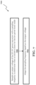
- Fig. 7 depicts a flow chart of a method 700 to operate a power converter in a low power burst mode.
- the method 700 to operate a DC-DC power converter in a low power burst mode comprises at a step 702 sampling an output voltage of the DC-DC power converter with a sampling frequency to determine when to initiate a burst for the low power burst mode; and at a step 704 adapting the sampling frequency based on the output voltage.
- Systems other than power converters that are operated in a burst or other forms of discrete corrections may be adaptively sampled by monitoring an output variable of the system and adjusting the sampling frequency of the output variable according to measurements of the output variable.
- temperature control that accomplished by an actuator (such as a heater) operating in bursts could be monitored by sampling the temperature and adjusting the sampling rate.
- a linear voltage regulator where the gate signal of the output MOS is driven by a capacitor may have a circuit providing "up" or "down" pulses according to an output voltage monitor, which may turned on according to an adaptive sampling frequency.
- Example 1 A method to operate a DC-DC power converter in a low power burst mode, the method including sampling an output voltage of the DC-DC power converter with a sampling frequency to determine when to initiate a burst for the low power burst mode; and adapting the sampling frequency based on the output voltage.
- Example 2 The method of Example 1, further including initiating a burst when the output voltage falls below a voltage threshold.
- Example 3 The method of Example 1 and Example 2, further including increasing the sampling frequency when the output voltage falls below a lower voltage threshold.
- Example 4 The method of Example 1 through Example 3, further including, wherein adapting the sampling frequency includes increasing the sampling frequency in response to an increase in an electric load powered by the output voltage.
- Example 5 The method of Example 1 through Example 4, wherein adapting the sampling frequency includes decreasing the sampling frequency in response to a decrease in an electric load powered by the output voltage.
- Example 6 The method of Example 1 through Example 5, further including counting a number of consecutive samples of the output voltage that do not trigger a burst; determining that the number exceeds an upper threshold; and wherein adapting the sampling frequency includes lowering the sampling frequency.
- Example 7 The method of Example 1 through Example 6, wherein the upper threshold is equal to 3
- Example 8 The method of Example 1 through Example 8, further including tracking a ratio of samples of the output voltage to bursts; determining that the ratio is too high; and wherein adapting the sampling frequency includes lowering the sampling frequency.
- Example 9 The method of Example 1 through Example 8, further including tracking a ratio of samples of the output voltage to bursts; determining that the ratio is too low; and wherein adapting the sampling frequency includes increasing the sampling frequency.
- Example 10 The method of Example 1 through Example 9, further including determining that a number of samples of the output voltage occurring between a first burst and a second burst is less than a lower threshold; and wherein adapting the sampling frequency includes increasing the sampling frequency.
- Example 11 The method of Example 1 through Example 10, further including determining that bursts have been initiated for two consecutive samples of the output voltage; and wherein adapting the sampling frequency includes increasing the sampling frequency.
- Example 12 A system to set a sampling frequency of an output voltage of a DC-DC power converter during a low power burst mode of the DC-DC power converter, the system including: a frequency-adaptation circuit configured to receive a clock signal having a first frequency and output an adapted clock signal having an adapted frequency that depends on the output voltage of the DC-DC power converter; and a voltage-monitoring circuit enabled by the adapted clock signal to sample the output voltage of the DC-DC power converter with the adapted frequency.
- Example 13 The system of Example 12 further including, a control logic circuit configured to receive the output voltage sampled by the voltage-monitoring circuit and communicate a frequency-selection signal to the frequency-adaptation circuit, the frequency-adaptation circuit being configured to adjust the adapted frequency according to changes in the frequency-selection signal and the frequency-selection signal being determined from the output voltage sampled by the voltage-monitoring circuit.
- a control logic circuit configured to receive the output voltage sampled by the voltage-monitoring circuit and communicate a frequency-selection signal to the frequency-adaptation circuit, the frequency-adaptation circuit being configured to adjust the adapted frequency according to changes in the frequency-selection signal and the frequency-selection signal being determined from the output voltage sampled by the voltage-monitoring circuit.
- Example 14 The system of Example 12 and Example 13, further including, wherein the control logic circuit is configured to output a burst-command signal when the output voltage falls below a voltage threshold.
- Example 15 The system of Example 12 to Example 14, wherein the frequency-adaptation circuit includes: a clock divider configured to receive the clock signal at a clock-signal input and configured to output a number of signals having frequencies that are quotients of the clock signal; and a multiplexer configured to receive the number of signals and select one of the number of signals to output as the adapted clock signal based on a frequency-selection signal that is determined from the output voltage sampled by the voltage-monitoring circuit.
- a clock divider configured to receive the clock signal at a clock-signal input and configured to output a number of signals having frequencies that are quotients of the clock signal
- a multiplexer configured to receive the number of signals and select one of the number of signals to output as the adapted clock signal based on a frequency-selection signal that is determined from the output voltage sampled by the voltage-monitoring circuit.
- Example 16 The system of Example 12 to Example 15, wherein the number of signals is equal to eight and the frequency-selection signal is a three-bit signal.
- Example 17 A system to provide an adapted sampling frequency for sampling an output voltage of a DC-DC power converter in a low power burst mode, the system including: an oscillator configured to produce a clock signal; a frequency-adaptation circuit configured to receive the clock signal and output an adapted clock signal including the adapted sampling frequency, the adapted sampling frequency being determined by a frequency-selection signal; and a tracking circuit configured to receive data indicating when a burst for the low power burst mode is initiated and output the frequency-selection signal depending on the data.
- Example 18 The system of Example 17, wherein the frequency-adaptation circuit includes: a clock divider configured to receive the clock signal at a clock-signal input and configured to output a number of signals having frequencies that are quotients of the clock signal; and a multiplexer configured to receive the number of signals and the frequency-selection signal, the multiplexer being configured to select one of the number of signals to output as the adapted clock signal based on the frequency-selection signal.
- a clock divider configured to receive the clock signal at a clock-signal input and configured to output a number of signals having frequencies that are quotients of the clock signal
- a multiplexer configured to receive the number of signals and the frequency-selection signal, the multiplexer being configured to select one of the number of signals to output as the adapted clock signal based on the frequency-selection signal.
- Example 19 The system of Example 17 and 18, wherein the tracking circuit includes an up counter in communication configured to be incremented when bursts are initiated and reset when bursts are not initiated; and a saturating up-and-down counter configured to receive an overflow signal from the up counter and increment a count each time the up counter overflows, and configured to decrement the count when up counter is reset twice consecutively, the count be provided to the multiplexer as the frequency-selection signal.
- the tracking circuit includes an up counter in communication configured to be incremented when bursts are initiated and reset when bursts are not initiated; and a saturating up-and-down counter configured to receive an overflow signal from the up counter and increment a count each time the up counter overflows, and configured to decrement the count when up counter is reset twice consecutively, the count be provided to the multiplexer as the frequency-selection signal.
- Example 20 The system of Example 17 through Example 19, wherein the frequency-select signal is a 3-bit signal, the up counter is a 2-bit counter, and the saturating up-and-down counter is a 3-bit counter.
Landscapes
- Engineering & Computer Science (AREA)
- Power Engineering (AREA)
- Dc-Dc Converters (AREA)
Abstract
Description
- The present invention relates generally to systems and method to adapt a sampling frequency for an output of a power converter in a low-power burst mode of operation.
- Power converters may operate in a low-power burst mode to conserve power resources. When a burst mode is enabled, the power converter is turned on and off as needed to maintain a minimum voltage level, which uses less power than continuous operation. The bursts are used as needed to sustain an output of the converter.
- In discrete-time burst modes, the voltage level is monitored to determine whether a burst is needed by sampling the output of the power converter. Monitoring circuits, and their auxiliaries, are turned on with a sampling frequency. If the sampling frequency is too low, transient fluctuations in the output load maybe missed. If the sampling frequency in too high, resources may be wasted unnecessarily turning monitoring equipment on and off. The efficiency and efficacy of the burst mode is thus impacted by the sampling frequency.
- Therefore, an aim of the invention is to overcome the limitations and shortcomings of the prior art.
- According to the invention, there are provided a method to operate a device, in particular a DC-DC power converter, in a low power burst mode and a system to set a sampling frequency of an output voltage of a device, in particular a DC-DC power converter, during a low power burst mode of the device, as defined in the accompanying claims.
- For the understanding of the present invention, and the advantages thereof, reference is now made to the following descriptions taken in conjunction with the accompanying drawings, in which:
-
Fig. 1 depicts a system for operating a DC-DC power converter in a low-power burst mode; -
Fig. 2 generally depicts a system to adaptively set a sampling frequency of the regulated voltage of an electric load during a low power burst mode of an embodiment; -
Fig. 3 depicts in more detail the system to set a sampling frequency of the regulated voltage of an electric load during a low power burst mode offigure 2 ; -
Fig. 4 illustrates a flow chart depicting a method to operate a power converter in an adaptively-sampled low-power burst mode; -
Fig. 5 illustrates a flow chart depicting a method to implement the observation window of an adaptively-sampled low-power burst mode; -
Fig. 6 depicts a system to adapt a sampling frequency for the output of a power converter in a low power burst mode; and -
Fig. 7 depicts a flow chart of the steps method to operate a power converter in a low power burst mode. - DC-DC power converters have many known uses, for example, providing regulated controlled output voltage from an unregulated input voltage. Unfortunately, DC-DC converters become less efficient when they have low output power (low current or voltage) as the ratio of switching losses to the output power increases. DC-DC converters may be configured to operate in a low-power burst mode to improve the efficiency of the power converter during low power operation of a device.
-
Fig. 1 depicts asystem 100 for operating a DC-DC power converter in a discrete-time low-power burst mode. - The
system 100 includes apower source 102 to supply an unregulated input voltage (VIN) to a DC-DC converter bridge 104. During normal operation, the DC-DC converter bridge 104 provides a regulated output voltage (VOUT) to anoutput 106 based on adriving signal 108A. - During low power operation, the DC-
DC converter bridge 104 is only driven in sporadic bursts when output needs to be restored to a proper level for low power operation. Thesystem 100 utilizes less power in between bursts than it would during normal operation when the DC-DC converter bridge 104 is driven continuously, thereby providing some power efficiencies. However, these efficiencies are limited by the sampling frequency used to monitor the need for power. - In the
system 100, the sampling frequency is determined by aclock signal 114A. Theclock signal 114A is received by acontrol logic circuit 110. Thecontrol logic circuit 110 periodically enables sampling of the output of the DC-DC converter bridge 104 according to the frequency of theclock signal 114A by providing an enablingsignal 110B to avoltage monitor 116 and auxiliaryanalog block 118. The auxiliaryanalog block 118 may include components that are also for sampling the output voltage to support operation of thevoltage monitor 116 and initiating bursts. Thevoltage monitor 116 senses the voltage at theoutput 106 and communicates with thecontrol logic circuit 110. Thecontrol logic circuit 110 triggers acommand signal 110A to abridge driver 108 to initiate a burst, when needed. Thebridge driver 108 responds to drive the DC-DC converter bridge 104 according to the command signal, which raises the voltage level at theoutput 106. - The need for a burst is determined by the level of the output voltage sensed by the
voltage monitor 116. If sampled voltage falls below a threshold, a burst is initiated. Otherwise, thevoltage monitor 116 and auxiliary circuits are powered down to wait for the next sample. Thevoltage monitor 116 and auxiliaryanalog blocks 118 consume power each time they sample the output voltage. More sampling thus equals more power consumption. As a result, the higher the sampling frequency of the output voltage, the less efficient the burst mode becomes. However, if the sampling frequency is too low, transient fluctuations in the output voltage may be missed, thereby creating complications in thesystem 100 or other devices that receive the regulated power at theoutput 106. A static sampling frequency limits the efficiency of the system because the sampling remains the same despite changes to the load. - The efficiency of a DC-DC converter may be improved by using an adaptable clock signal to determine the sampling frequency used to monitor the output voltage. An adaptable clock signal may adjust as the load varies so unneeded samples are cut out when the output load declines. And, the sampling rate may be increased when the load increases, so transient fluctuations are not missed.
- An adaptable sampling frequency may also produce more predictable power-efficiency benefits. With a static sampling frequency, the efficiency of the system changes because the ration of bursts and samples will vary as the load varies. However, an adapted frequency allows the ratio of bursts to samples to be maintained more consistently, or even pegged to each other. The efficiency of such devices and methods may thus be more predictable.
- In various situations, it may be advantageous to maintain the sampling frequency so that it is at least twice that of the burst frequency in accordance with the general Shannon theorem for sampling, which states that to reconstruct a signal the sampling frequency must be at least twice the signal frequency.
-
Fig. 2 depicts asystem 200 to adaptively set a sampling frequency of the regulated voltage of an electric load during a low power burst mode . - The
system 200 includes afrequency adaptation circuit 215. Thefrequency adaptation circuit 215 may be digital. Thefrequency adaptation circuit 215 receives aclock signal 214A. Thefrequency adaption circuit 215 is also in communication (directly or indirectly) with avoltage monitor 216. - As will be appreciated, the voltage monitor may be realized in different ways. For example, a comparator may compare output voltage to a reference voltage, or the output voltage may be converted in an equivalent current and then compared to a reference current.
- An
output signal 216A from thevoltage monitor 216 may be supplied to thefrequency adaptation circuit 215. Thevoltage monitor 216, when enabled, may sense the voltage at theoutput 206 of a power converter (like a DC-DC power converter). - The
frequency adaptation circuit 215 outputs an adaptedclock signal 215A that depends on theclock signal 214A and the voltage at theoutput 206 sensed by thevoltage monitor 216. - The frequency of the
clock signal 214A may be constant. - The adapted
clock signal 215A can be adapted to account for changes in the load coupled to a DC-DC converter to improve the power efficiency of thesystem 200. - For example, the frequency of the adapted
clock signal 215A may be increased as the load increases and be decreased as the load decreases. The adaptedclock signal 215A may then be used to enable and disable thevoltage monitor 216 and the auxiliaryanalog blocks 218 to sample the output voltage with a frequency determined by the adaptedclock signal 215A. Depending on the voltage at theoutput 206, a burst may or may not be initiated. - The
frequency adaptation circuit 215 may comprise a programmable frequency divider that divides the frequency of the clock signal 214A to generate the adaptedclock signal 215A. The divisors for the programmable frequency divider may be determined based on the sampling of the voltage level sensed by thevoltage monitor 216. - A programmable frequency multiplier may be used to generate an adapted
clock signal 215A that is a product of theclock signal 214A. Multipliers for the programmable frequency multiplier may be determined based on the voltage level sensed by thevoltage monitor 216. -
Fig. 3 depicts more in detail an embodiment of thesystem 200. - In this embodiment, the
system 200 includes a DC-DC converter bridge 204. The DC-DC converter bridge 204 receives a voltage supply (VIN) 202. The DC-DC converter bridge 204 provides a regulated output voltage to anoutput 206 based on adriving signal 208A. - During low power burst-mode operation, the DC-
DC converter bridge 204 is driven in sporadic bursts when more power is needed, which is determined by the voltage level sensed at theoutput 206 by thevoltage monitor 216. The voltage monitor 216 monitors the voltage at theoutput 206 with a frequency that is determined by the adaptedclock signal 215A. - The
system 200 ofFig. 3 includes anoscillator 214 to provide theclock signal 214A to thefrequency adaption circuit 215. - The
oscillator 214 may comprise a low frequency oscillator. It may be advantageous to utilize a low frequency oscillator to limit power requirements of theoscillator 214. - Operation of the
oscillator 214 may be triggered by a burst-mode enablesignal 217. The burst-mode enablesignal 217 may comprise a flag that indicates when thesystem 200 is in a low-power mode (such as a standby mode). It will also be appreciated that the burst-mode enablesignal 217 may also be triggered by operating conditions such as the current drawn by the load. In various situations, other conditions may trigger a change to the burst mode of operation. - When in the low-power burst mode (for example, when enabled by burst-mode enable signal 217), the
oscillator 214 outputs aclock signal 214A. In various situations, theoscillator 214 may only operate when enabled by the burst-mode enablesignal 217. - The
clock signal 214A is received by thefrequency adaptation circuit 215, which may adapt the signal based on the output load as measured by the sampling of the regulated output voltage. - The
frequency adaptation circuit 215 here outputs an adaptedclock signal 215A to acontrol logic circuit 210. Thecontrol logic circuit 210 may then enable sampling of the output of the DC-DC converter bridge 204 according to the frequency of the adaptedclock signal 215A by providing an enablingsignal 210B to thevoltage monitor 216 andauxiliary analog block 218. - The
auxiliary analog block 218 may include a reference-voltage generator for thevoltage monitor 216, biasing circuitry for thevoltage monitor 216, an oscillator used to time output bursts, and other circuitry to support operation of the voltage monitor 216 or converter. - The adapted
clock signal 215A may have an initial or default setting. For example, the initial frequency of the adaptedclock signal 215A may be equal to the frequency of theclock signal 214A. - The voltage monitor 216 may sense the voltage at the
output 206 when enabled and communicate with thecontrol logic circuit 210.Output signal 216A from thevoltage monitor 216 is here provided to thecontrol logic circuit 210. Thecontrol logic circuit 210 may trigger acommand signal 210A to abridge driver 208 to initiate a burst, when needed, based on the voltage sampled. The burst may raise the voltage level at theoutput 206. - The need for a burst may be determined depending on the output voltage sensed by the
voltage monitor 216. If sampled voltage falls below a threshold, thevoltage monitor 216 sends a corresponding information throughoutput signal 216A to thecontrol logic circuit 210, A burst may be initiated by thecontrol logic circuit 210 by sending thecommand signal 210A to thebridge driver 208. And, in turn, thebridge driver 208 may provide switching signals for operation of the DC-DC converter bridge 204. If the output voltage VOUT sampled by thevoltage monitor 216 is above a threshold, thevoltage monitor 216 and auxiliary circuits may be powered down to wait for the next sample. - The voltage monitor 216 may communicate the voltage sampled at the
output 206 to thecontrol logic circuit 210 via theoutput signal 216A. Thecontrol logic circuit 210 may provide a frequency command, or frequency-selection signal 210C to thefrequency adaption circuit 215. In the alternative, theoutput signal 216A may be provided directly to afrequency adaptation circuit 215. - The frequency-
selection signal 210C may be adjusted depending on the voltage sampled at the output 206.Thefrequency adaption circuit 215 may change the frequency of the adaptedclock signal 215A depending on the frequency-selection signal 210C. For example, thefrequency adaption circuit 215 may comprise a frequency divider where theclock signal 215A has a frequency that is a quotient of the frequency of theclock signal 214A and a divisor. The divisor may be selected depending on the frequency-selection signal 210C. -
Fig. 4 illustrates a flow chart depicting amethod 400 to operate a power converter in an adaptively-sampled low-power burst mode. - At a
step 402, the burst mode is enabled. The burst mode may be enabled by burst-mode enablesignal 217. - At a
step 404,oscillator 214 is enabled. Theoscillator 214 may be enabled by the burst-mode enablesignal 217. - At a
step 406, the system waits to enable sampling of an output voltage a power converter. Samples may be triggered by a rising edge of an adapted clock signal. However, as will be appreciated, the falling edge of an adapted clock signal may be used or other time derived from an adapted clock signal. An adapted clock signal may have default or initial setting that determines the frequency an adapted clock signal before voltage at an output has been sampled. - Once triggered by the adapted clock signal, at a
step 408, the monitoring circuitry enters anobservation period 407 where thevoltage monitor 216 andauxiliary analog block 218 are enabled. - A burst may be initiated and performed at
step 410, if needed. And, the adapted clock signal may be adjusted atstep 412, if needed. - The observation window may be closed at
step 414 and thevoltage monitor 216 andauxiliary analog block 218 disabled. - At as
step 416, it is determined if the burst-mode is still enabled. This may be determined by the status of the burst-mode enablesignal 217. If the burst mode is still enabled after closing of the observation window, the method ofFig. 4 comprises returning to step 406 to wait for the adapted clock signal to trigger another observation window. As will be appreciated, this may occur at the next rising edge of the adaptedclock signal 215A. It may also be triggered by the falling edge of adaptedclock signal 215A, or at other times derived from the adaptedclock signal 215A. - Step 416 may be performed continuously or contemporaneous with other steps. For example, the burst-mode enable
signal 217 may be continuously monitored. This may allow a quicker response if the mode of operation changes. This maybe beneficial in various situations because auxiliary circuits may be activated to switch out of a burst mode. By continuously monitoring the mode of operation (or contemporaneously with other steps), any activations needed to switch modes may be initiated as soon as a change in mode is detected. This may reduce or eliminate a latency associated with switching modes. - If the burst mode is no longer enabled at
step 416, then the method ofFig. 4 proceeds to step 418. This may be determined by the status of the burst-mode enablesignal 217. At step 418, theoscillator 214 is disabled. And, atstep 420, the burst mode is exited. - The power converter may begin, or resume, standard operations.
-
Fig. 5 illustrates a flow chart depicting amethod 500 to implement the observation window of an adaptively-sampled low-power burst mode. -
Method 500 ofFig. 5 comprises at astep 502 opening an observation window. This may include enabling thevoltage monitor 216 andauxiliary analog block 218. This step may correspond to thestep 408 as discussed with reference toFig. 4 . -
Method 500 comprises at astep 504 evaluating the output voltage VOUT atoutput 206 of a power converter such as DC-DC converter bridge 204. This involves sensing the output voltage of the power converter according to known techniques and with known equipment. After evaluating the output voltage, the method comprises atstep 506 determining whether to initiate a burst. The output voltage detected by the voltage monitor may be compared with a minimum level or threshold for the output voltage. If the output voltage sensed atstep 504 is lower than the minimum level or threshold, a burst may be generated atstep 508. - After generation of the burst at
step 508, the voltage at the output may be detected again. The output voltage VOUT may again be compared with a minimum level or threshold to determine whether it is okay. The voltage monitor 216 may continuously detect the voltage at the output of the power converter while the observation window is open. - The burst may be continuously generated until the output voltage has reached a minimum level. The minimum value or threshold used for comparison at
step 510 maybe the same minimum level or threshold value used for comparison with the output voltage at step 506.Minimum value or threshold used for comparison atstep 510 may be a different minimum level or threshold value used for comparison with the output voltage atstep 506. For example, the voltage level to trigger a burst may be the same or different from the voltage level to determine whether additional bursts are needed. - If the output voltage at
step 510 does not exceed the threshold, the method is looped back to step 508 and generate another burst. This loop may continue until the output voltage is raised to a sufficient voltage level. - Once it has been determined that the voltage at the output has been sufficiently raised, it is determined at
step 512 whether to increase the frequency of the output voltage sampling. This may comprise increasing the frequency of the adapted clock signal. - As will be appreciated, considerations for determining whether to increase the sampling frequency may differ. There is a multitude of different ways to gauge whether the frequency of the adapted clock signal needs to be changed. Some examples are provided below. However, these examples are only provided for illustrative purposes. Other approaches may be utilized to adapt the sampling frequency of the regulated output voltage.
- Adaptive sampling maybe utilized to maintain a steady state between a ratio of bursts to samples. For example, the ratio of samples to bursts may be maintained by adaptive sampling at 2 to 1, 4 to 1, or in a range between 2 to 1 and 4 to 1. Any other ratio or range may be maintained with adaptive sampling of the output.
- The number of clock cycles (or observation windows) between bursts maybe tracked. If the number of clock cycles between bursts is lower than desired, this may indicate that the voltage output is not be sampled frequently enough and the frequency for sampling the output may be increased.
- If bursts are generated in consecutive observation windows, the frequency used for sampling the output voltage may be increased. For example, the number of cycles where bursts occur and the number of cycles where bursts do not occur may be tracked and compared with each other to determine whether to increase the frequency used for sampling. For example, if the number of cycles where bursts are needed is higher than desired relative to the number of cycles where bursts are needed, the frequency used for sampling may be increased.
- A determination about whether to increase a sampling frequency may depend on a voltage threshold for adapting the sampling frequency. The voltage detected at output of the power converter by the
voltage monitor 216 may be compared with the threshold to adapt the sampling frequency. The voltage threshold to adapt the sampling frequency may be lower than the level or threshold used to determine whether to generate a burst. If the output level falls below this lower threshold, the frequency may be increased. - A determination about whether to increase a sampling frequency may depend on the number of bursts needed to increase the voltage level. For example, each loop through
step 508 may be counted. If the number of bursts (or loops through step 508) is greater than a threshold, the frequency for sampling the output may be increased. The number of bursts provided in each cycle may also be counted directly. - A rolling average of the number of observation window opened between bursts may be tracked. If this number is less than desired (lower than a threshold) the frequency may be increased.
- If it is determined at
step 512 that the frequency used to sample the output voltage needs to increased, then the frequency may be increased at step 514. If it is determined atstep 512 that the frequency used to sample the output voltage does not need to be increased, then step 514 may skipped. And, the observation window may be closed atstep 516. Closing the observation window may entail disabling thevoltage monitor 216 andauxiliary analog block 218. - Returning to step 506, if it is determined that a burst is not needed, it is determined at
step 515 whether to decrease the frequency at which the output voltage is sampled. If it is determined atstep 515 that frequency will be adjusted, the method ofFig. 5 proceeds to step 514. If it is determined that the frequency will not be adjusted, the method ofFig. 5 proceeds to step 516. As will be appreciated, the process for determining whether to decrease the frequency may differ. There are many different ways to gauge whether the frequency of the adapted clock signal needs to be decreased. Some examples are provided below. However, these examples are only provided for explanatory purposes. Other approaches may be utilized. - For example, the number of clock cycles (or observation windows) between bursts may be tracked. If the number of clock cycles is higher than desired, this may indicate that the output of the converter is being sampled too much. The frequency for sampling the output may be decreased.
- The number of cycles where bursts occur and the number of cycles where bursts do not occur may be tracked and compared with each other to determine whether to decrease the frequency used for sampling. For example, if the number of cycles where no bursts are needed is higher than desired relative to the number of cycles where bursts are needed, the frequency used for sampling may be decreased.
- The voltage output may be compared with another voltage threshold that is higher than the minimum level or threshold used to determine whether to generate a burst. If the output level stays above this threshold, this may indicate that output is being sampled more than is ideal and the sampling rate may be decreased. For example, if the voltage level falls below the higher threshold and remains above a threshold used to determine whether to generate a burst, the sampling frequency may be decreased. A rolling average of the number of observation windows between bursts may be tracked and the frequency may be decreased if this number is higher than desired. Decreasing the sampling frequency may comprise adjusting the adapted clock signal.
- After it is determined at
step 515 whether or not to decrease the sampling frequency of the output, the observation window is closed atstep 516. This may comprise disabling the voltage monitor. Auxiliary circuits may also be disabled. -
Fig. 6 depicts asystem 600 to adapt a sampling frequency for the output of a power converter in a low power burst mode. - The
system 600 offig. 6 includesoscillator 214. Theoscillator 214 may comprise a low speed clock. Thesystem 600 further comprises aclock divider 602 and a multiplexer,MUX 604. Avoltage monitor 216 is be used in thesystem 600 to detect the voltage at theoutput 206 of a DC-DC power converter. Thesystem 600 further comprisesbridge driver 208 and avoltage check circuit 606. - The
system 600 of Fig. 8 further comprises an upcounter 608 and an up/downcounter 610. The up/downcounter 610 may comprise a saturating up/down counter. - The
oscillator 214 may be enabled by burst mode enable signal 217 (not shown inFig. 6 ). When enabled, theoscillator 214 supplies theclock signal 214A to theclock divider 602. Theclock divider 602, in turn, outputs a number of signals. - Each of the signals may have a frequency equal to the quotient of the frequency of the
clock signal 214A and a divisor. For example, afirst signal 602A may have the same frequency as theclock signal 214A. Asecond signal 602B may have a frequency equal to the frequency of theclock signal 214A divided by 2. Athird signal 602C may have a frequency equal to the frequency of theclock signal 214A divided by 4. AnNth output 602N may have a frequency equal to the frequency of theclock signal 214A divided by a number X. The value for the number X may be derived from the number of outputs. For example, X may be equal to 2N or 2(N-1). For example, theclock divider 602 may have 8 outputs and X may be equal to 128. As will be appreciated, the number of signals output from theclock divider 602 may be different. And, as will also be appreciated, the divisors may vary. - The signals output from the
clock divider 602 may be provided to aMUX 604. TheMUX 604 outputs one of the signals depending on a frequency-selection signal 603. The frequency-selection signal 603 may comprise three bits. The number of bits of the frequency-selection signal may be different. - The MUX comprises a
first input 604A, asecond input 604B, and anNth input 604N. However, theMUX 604 may have different numbers of inputs. The number of inputs of theMUX 604 may correspond to the number of output signals produced by theclock divider 602. The inputs may correspond to a bit value. The number of bits of the frequency-selection signal may be at least big enough to select each potential input to the MUX. For example, an 8-input MUX may have a 3-bit frequency-selection signal. When the frequency-selection signal 603 transmits a bit value that corresponds to the input, theMUX 604 may output the corresponding input. For example, if thefirst input 604A is corresponded to a bit value of "000," the MUX will output the signal provided to thefirst input 604A when the frequency-selection signal transmits a "000." The output of theMUX 604 may comprise the adaptedclock signal 215A. - The voltage monitor 216 is enabled by the adapted
clock signal 215A. For example, the when the adaptedclock signal 215A is high, thevoltage monitor 216 may be enabled. The adaptedclock signal 215A may also enable auxiliary analog blocks 218 that are not shown inFig. 6 . - When enabled, the
voltage monitor 216 detects the voltage atoutput 206 of the converter. Anoutput signal 216A from thevoltage monitor 216 is transmitted to avoltage check circuit 606 where the voltage detected by thevoltage monitor 216 is checked to determine if a burst is needed to raise the output voltage at theoutput 206. If the voltage at theoutput 206 is okay (no burst is needed), a no-burst signal 606A is asserted. If the voltage at theoutput 206 is not okay (a burst is needed), aburst signal 606B is asserted. Thevoltage check circuit 606 may check the voltage with the frequency of the adaptedclock signal 215A. The adaptedclock signal 215A may be provided to thevoltage check circuit 606. - The no-
burst signal 606A is here provided to thevoltage monitor 216. The no-burst signal 606A may disable thevoltage monitor 216. This may save power by turning off the voltage monitor 216 when it is not needed. The no-burst signal 606A may also disable auxiliary analog blocks 218 (not shown inFig. 6 ). Theburst signal 606B may be provided to thebridge driver 208. When asserted theburst signal 608B may be cause thebridge driver 208 to initiate a burst. - The no-
burst signal 606A and theburst signal 606B are here provided to an upcounter 608. The up counter 608 may be used to track how often bursts are required by the power converter relative to periods where no bursts are needed. When asserted, the no-burst signal 606A may increment theup counter 608. And, when asserted, theburst signal 606B may reset the up counter 608.When the up counter 608 overflows, anoverflow signal 608A is here provided to an up/downcounter 610. For a two-bit bit counter, the up counter 608 overflows when samples without bursts exceeds samples with bursts by 4.However, the up counter may comprise a different number of bits. - An
overflow signal 608A, when asserted, causes the up/down counter 610 to be incremented, which in turn changes the value of the frequency-selection signal 603. TheMUX 604 may be configured so that it selects a slower signal when the frequency-selection signal is incremented thereby adapting the frequency of the adaptedclock signal 215A based on the voltage at theoutput 206 so the adapted clock signal will be slowed down as less bursts are needed to maintain the voltage at theoutput 206 at a desired level. - As will be appreciated, the number of bits of the
up counter 608 may vary. The size of the up counter may impact when anoverflow signal 608A is asserted thus impacting when the up/down counter is incremented and how often the adaptedclock signal 215A changes. - The up counter 608 may also be configured to assert a
decrement signal 608B after consecutive resets. The number of resets needed to trigger assertion of thedecrement signal 608B may be different. For example, two consecutive resets of theup counter 608 may trigger assertion of thedecrement signal 608B. In the alternative, three consecutive resets of theup counter 608 may trigger assertion of thedecrement signal 608B. Thedecrement signal 608B may be triggered by more than three consecutive resets. - The
decrement signal 608B, when asserted, causes the up/down counter 610 to be decremented thus altering the frequency-selection signal 603 and the output of theMUX 604. The MUX may be configured so that it selects a faster signal when the frequency-selection signal is decremented thereby adapting the frequency of the adaptedclock signal 215A based on the voltage at theoutput 206 so the adapted clock signal will be speed up as more bursts are needed to maintain the voltage at theoutput 206 at a desired level. - As will be appreciated, components of the
system 600 may differ in different embodiments. For example, the sizes of the up/downcounter 610 and upcounter 608 may be different. Different sizes of the up counter may be used so the adaptedclock signal 215A is changed more or less often. The size of the up/downcounter 610 may be corresponded to the number of different input signals provided to theMUX 604. Thefrequency adaption circuit 215 may comprise aMUX 604 andclock divider 602. -
Fig. 7 depicts a flow chart of amethod 700 to operate a power converter in a low power burst mode. - The
method 700 to operate a DC-DC power converter in a low power burst mode comprises at astep 702 sampling an output voltage of the DC-DC power converter with a sampling frequency to determine when to initiate a burst for the low power burst mode; and at astep 704 adapting the sampling frequency based on the output voltage. - Finally, it is clear that numerous variations and modifications may be made to the method and system described and illustrated herein, all falling within the scope of the invention as defined in the attached claims.
- For example, the various embodiments described above can be combined to provide further embodiments.
- Systems other than power converters that are operated in a burst or other forms of discrete corrections may be adaptively sampled by monitoring an output variable of the system and adjusting the sampling frequency of the output variable according to measurements of the output variable. For example, temperature control that accomplished by an actuator (such as a heater) operating in bursts could be monitored by sampling the temperature and adjusting the sampling rate. In another example, a linear voltage regulator where the gate signal of the output MOS is driven by a capacitor may have a circuit providing "up" or "down" pulses according to an output voltage monitor, which may turned on according to an adaptive sampling frequency.
- Example 1. A method to operate a DC-DC power converter in a low power burst mode, the method including sampling an output voltage of the DC-DC power converter with a sampling frequency to determine when to initiate a burst for the low power burst mode; and adapting the sampling frequency based on the output voltage.
- Example 2. The method of Example 1, further including initiating a burst when the output voltage falls below a voltage threshold.
- Example 3. The method of Example 1 and Example 2, further including increasing the sampling frequency when the output voltage falls below a lower voltage threshold.
- Example 4. The method of Example 1 through Example 3, further including, wherein adapting the sampling frequency includes increasing the sampling frequency in response to an increase in an electric load powered by the output voltage.
- Example 5. The method of Example 1 through Example 4, wherein adapting the sampling frequency includes decreasing the sampling frequency in response to a decrease in an electric load powered by the output voltage.
- Example 6. The method of Example 1 through Example 5, further including counting a number of consecutive samples of the output voltage that do not trigger a burst; determining that the number exceeds an upper threshold; and wherein adapting the sampling frequency includes lowering the sampling frequency.
- Example 7. The method of Example 1 through Example 6, wherein the upper threshold is equal to 3
- Example 8. The method of Example 1 through Example 8, further including tracking a ratio of samples of the output voltage to bursts; determining that the ratio is too high; and wherein adapting the sampling frequency includes lowering the sampling frequency.
- Example 9. The method of Example 1 through Example 8, further including tracking a ratio of samples of the output voltage to bursts; determining that the ratio is too low; and wherein adapting the sampling frequency includes increasing the sampling frequency.
- Example 10. The method of Example 1 through Example 9, further including determining that a number of samples of the output voltage occurring between a first burst and a second burst is less than a lower threshold; and wherein adapting the sampling frequency includes increasing the sampling frequency.
- Example 11. The method of Example 1 through Example 10, further including determining that bursts have been initiated for two consecutive samples of the output voltage; and wherein adapting the sampling frequency includes increasing the sampling frequency.
- Example 12. A system to set a sampling frequency of an output voltage of a DC-DC power converter during a low power burst mode of the DC-DC power converter, the system including: a frequency-adaptation circuit configured to receive a clock signal having a first frequency and output an adapted clock signal having an adapted frequency that depends on the output voltage of the DC-DC power converter; and a voltage-monitoring circuit enabled by the adapted clock signal to sample the output voltage of the DC-DC power converter with the adapted frequency.
- Example 13. The system of Example 12 further including, a control logic circuit configured to receive the output voltage sampled by the voltage-monitoring circuit and communicate a frequency-selection signal to the frequency-adaptation circuit, the frequency-adaptation circuit being configured to adjust the adapted frequency according to changes in the frequency-selection signal and the frequency-selection signal being determined from the output voltage sampled by the voltage-monitoring circuit.
- Example 14. The system of Example 12 and Example 13, further including, wherein the control logic circuit is configured to output a burst-command signal when the output voltage falls below a voltage threshold.
- Example 15. The system of Example 12 to Example 14, wherein the frequency-adaptation circuit includes: a clock divider configured to receive the clock signal at a clock-signal input and configured to output a number of signals having frequencies that are quotients of the clock signal; and a multiplexer configured to receive the number of signals and select one of the number of signals to output as the adapted clock signal based on a frequency-selection signal that is determined from the output voltage sampled by the voltage-monitoring circuit.
- Example 16. The system of Example 12 to Example 15, wherein the number of signals is equal to eight and the frequency-selection signal is a three-bit signal.
- Example 17. A system to provide an adapted sampling frequency for sampling an output voltage of a DC-DC power converter in a low power burst mode, the system including: an oscillator configured to produce a clock signal; a frequency-adaptation circuit configured to receive the clock signal and output an adapted clock signal including the adapted sampling frequency, the adapted sampling frequency being determined by a frequency-selection signal; and a tracking circuit configured to receive data indicating when a burst for the low power burst mode is initiated and output the frequency-selection signal depending on the data.
- Example 18. The system of Example 17, wherein the frequency-adaptation circuit includes: a clock divider configured to receive the clock signal at a clock-signal input and configured to output a number of signals having frequencies that are quotients of the clock signal; and a multiplexer configured to receive the number of signals and the frequency-selection signal, the multiplexer being configured to select one of the number of signals to output as the adapted clock signal based on the frequency-selection signal.
- Example 19. The system of Example 17 and 18, wherein the tracking circuit includes an up counter in communication configured to be incremented when bursts are initiated and reset when bursts are not initiated; and a saturating up-and-down counter configured to receive an overflow signal from the up counter and increment a count each time the up counter overflows, and configured to decrement the count when up counter is reset twice consecutively, the count be provided to the multiplexer as the frequency-selection signal.
- Example 20. The system of Example 17 through Example 19, wherein the frequency-select signal is a 3-bit signal, the up counter is a 2-bit counter, and the saturating up-and-down counter is a 3-bit counter.
Claims (15)
- A method to operate a device, in particular a DC-DC power converter (204), in a low power burst mode, the method comprising:sampling an output voltage of the device with a sampling frequency to determine when to initiate a burst for the low power burst mode; andadapting the sampling frequency based on the output voltage.
- The method of claim 1, further comprising initiating a burst when the output voltage falls below a voltage threshold.
- The method of claim 2, further comprising increasing the sampling frequency when the output voltage falls below a lower voltage threshold.
- The method of any of the preceding claims, wherein adapting the sampling frequency comprises increasing the sampling frequency in response to an increase in an electric load powered by the output voltage.
- The method of any of the preceding claims, wherein adapting the sampling frequency comprises decreasing the sampling frequency in response to a decrease in an electric load powered by the output voltage.
- The method of claim 1, further comprising:counting a number of consecutive samples of the output voltage that do not trigger a burst;determining that the number exceeds an upper threshold; andwherein adapting the sampling frequency comprises lowering the sampling frequency.
- The method of any of the preceding claims, further comprising:tracking a ratio of samples of the output voltage to bursts;determining that the ratio is too high; andwherein adapting the sampling frequency comprises lowering the sampling frequency.
- The method of any of the preceding claims, further comprising:tracking a ratio of samples of the output voltage to bursts;determining that the ratio is too low; andwherein adapting the sampling frequency comprises increasing the sampling frequency.
- The method of any of the preceding claims, further comprising:determining that a number of samples of the output voltage occurring between a first burst and a second burst is less than a lower threshold; andwherein adapting the sampling frequency comprises increasing the sampling frequency.
- The method of any of the preceding claims, further comprising:determining that bursts have been initiated for two consecutive samples of the output voltage; andwherein adapting the sampling frequency comprises increasing the sampling frequency.
- A system (200) to set a sampling frequency of an output voltage of a device, in particular a DC-DC power converter (204), during a low power burst mode of the device, the system comprising:a frequency-adaptation circuit (215) configured to receive a clock signal (214A) having a first frequency and output an adapted clock signal (215A) having an adapted frequency that depends on the output voltage (VOUT) of the device; anda voltage-monitoring circuit (216) enabled by the adapted clock signal to sample the output voltage of the device with the adapted frequency.
- The system of the preceding claim, further comprising a control logic circuit (210) configured to receive the output voltage (VOUT) sampled by the voltage-monitoring circuit (216) and communicate a frequency-selection signal (216A) to the frequency-adaptation circuit (215), the frequency-adaptation circuit being configured to adjust the adapted frequency according to changes in the frequency-selection signal and the frequency-selection signal being determined from the output voltage sampled by the voltage-monitoring circuit.
- The system of the preceding claim, wherein the control logic circuit (210) is configured to output a burst-command signal when the output voltage falls below a voltage threshold.
- The system of any of claims 11-13, wherein the frequency-adaptation circuit (215) comprises:a clock divider (602) configured to receive the clock signal (214A) at a clock-signal input and configured to output a number of signals having frequencies that are quotients of the clock signal; anda multiplexer (604) configured to receive the number of signals and select one of the number of signals to output as the adapted clock signal based on a frequency-selection signal that is determined from the output voltage (VOUT) sampled by the voltage-monitoring circuit (216).
- A system to provide an adapted sampling frequency for sampling an output voltage (VOUT) of a device, in particular a DC-DC power converter (204), in a low power burst mode, the system comprising:an oscillator (214) configured to produce a clock signal (214A);a frequency-adaptation circuit (215) configured to receive the clock signal and output an adapted clock signal comprising the adapted sampling frequency, the adapted sampling frequency being determined by a frequency-selection signal; anda tracking circuit configured to receive data indicating when a burst for the low power burst mode is initiated and output the frequency-selection signal depending on the data.
Applications Claiming Priority (1)
| Application Number | Priority Date | Filing Date | Title |
|---|---|---|---|
| US17/387,296 US11955877B2 (en) | 2021-07-28 | 2021-07-28 | Methods and devices for adaptive output sampling for power converters |
Publications (1)
| Publication Number | Publication Date |
|---|---|
| EP4125198A1 true EP4125198A1 (en) | 2023-02-01 |
Family
ID=82781103
Family Applications (1)
| Application Number | Title | Priority Date | Filing Date |
|---|---|---|---|
| EP22187477.9A Pending EP4125198A1 (en) | 2021-07-28 | 2022-07-28 | Methods and devices for adaptive output sampling for power converters |
Country Status (3)
| Country | Link |
|---|---|
| US (1) | US11955877B2 (en) |
| EP (1) | EP4125198A1 (en) |
| CN (1) | CN115694128A (en) |
Families Citing this family (1)
| Publication number | Priority date | Publication date | Assignee | Title |
|---|---|---|---|---|
| US12136883B2 (en) * | 2021-09-30 | 2024-11-05 | Stmicroelectronics S.R.L. | Method for operating in burst mode active clamp flyback converters and corresponding active clamp flyback converter apparatus |
Citations (7)
| Publication number | Priority date | Publication date | Assignee | Title |
|---|---|---|---|---|
| US6366070B1 (en) * | 2001-07-12 | 2002-04-02 | Analog Devices, Inc. | Switching voltage regulator with dual modulation control scheme |
| US20110176335A1 (en) * | 2010-01-21 | 2011-07-21 | Li Zeng | Resonant converters and burst mode control method thereof |
| US20150003117A1 (en) * | 2013-06-26 | 2015-01-01 | Stmicroelectronics S.R.L. | Method of controlling a switching converter in burst mode and related controller for a switching converter |
| US20150311795A1 (en) * | 2014-04-28 | 2015-10-29 | Intersil Americas LLC | Current pulse count control in a voltage regulator |
| US9893602B2 (en) * | 2014-02-26 | 2018-02-13 | Infineon Technologies Austria Ag | Switched-mode power converter with sampled feedback signal |
| US20180048320A1 (en) * | 2016-08-09 | 2018-02-15 | Freescale Semiconductor, Inc. | Switching power converter |
| US20190229626A1 (en) * | 2018-01-23 | 2019-07-25 | Apple Inc. | Adaptive Wakeup Time Control In Burst Mode Of A Primary Side Regulated Flyback Converter |
Family Cites Families (5)
| Publication number | Priority date | Publication date | Assignee | Title |
|---|---|---|---|---|
| US20020057080A1 (en) * | 2000-06-02 | 2002-05-16 | Iwatt | Optimized digital regulation of switching power supply |
| US8274266B2 (en) | 2009-08-14 | 2012-09-25 | Linear Technology Corporation | Switch mode power supply with dynamic topology |
| US9812960B2 (en) * | 2015-12-29 | 2017-11-07 | Texas Instruments Incorporated | Methods and apparatus for a low standby current DC-DC power controller with improved transient response |
| EP3920398A1 (en) * | 2020-06-05 | 2021-12-08 | Nxp B.V. | A controller for a power supply and a power supply |
| CN113162372B (en) * | 2020-12-31 | 2022-03-22 | 成都芯源系统有限公司 | Quasi-resonance controlled switch converter, controller and control method thereof |
-
2021
- 2021-07-28 US US17/387,296 patent/US11955877B2/en active Active
-
2022
- 2022-07-28 EP EP22187477.9A patent/EP4125198A1/en active Pending
- 2022-07-28 CN CN202210900128.8A patent/CN115694128A/en active Pending
Patent Citations (7)
| Publication number | Priority date | Publication date | Assignee | Title |
|---|---|---|---|---|
| US6366070B1 (en) * | 2001-07-12 | 2002-04-02 | Analog Devices, Inc. | Switching voltage regulator with dual modulation control scheme |
| US20110176335A1 (en) * | 2010-01-21 | 2011-07-21 | Li Zeng | Resonant converters and burst mode control method thereof |
| US20150003117A1 (en) * | 2013-06-26 | 2015-01-01 | Stmicroelectronics S.R.L. | Method of controlling a switching converter in burst mode and related controller for a switching converter |
| US9893602B2 (en) * | 2014-02-26 | 2018-02-13 | Infineon Technologies Austria Ag | Switched-mode power converter with sampled feedback signal |
| US20150311795A1 (en) * | 2014-04-28 | 2015-10-29 | Intersil Americas LLC | Current pulse count control in a voltage regulator |
| US20180048320A1 (en) * | 2016-08-09 | 2018-02-15 | Freescale Semiconductor, Inc. | Switching power converter |
| US20190229626A1 (en) * | 2018-01-23 | 2019-07-25 | Apple Inc. | Adaptive Wakeup Time Control In Burst Mode Of A Primary Side Regulated Flyback Converter |
Also Published As
| Publication number | Publication date |
|---|---|
| US11955877B2 (en) | 2024-04-09 |
| CN115694128A (en) | 2023-02-03 |
| US20230034912A1 (en) | 2023-02-02 |
Similar Documents
| Publication | Publication Date | Title |
|---|---|---|
| JP4825291B2 (en) | Adaptive voltage scaling clock generator for use in digital processing components and method of operation thereof | |
| US6868503B1 (en) | Adaptive voltage scaling digital processing component and method of operating the same | |
| US8008902B2 (en) | Hysteretic buck converter having dynamic thresholds | |
| US7888924B2 (en) | Combination continuous and discontinuous control of a power regulator | |
| EP1635445B1 (en) | Adaptive control for inductor based buck-boost voltage regulators | |
| US6548991B1 (en) | Adaptive voltage scaling power supply for use in a digital processing component and method of operating the same | |
| TWI668948B (en) | Methods of regulating voltage, switching voltage regulators and systems having the same, and integrated circuit chips for providing regulated voltages | |
| CN104426360B (en) | Regulation circuit and adjusting method for charge pump | |
| JPH0720968A (en) | Method for reduction of power consumption of computer by changing voltage and frequency dynamically | |
| EP1894076A2 (en) | Regulating switching regulators by load monitoring | |
| JP2009089578A5 (en) | ||
| US8769322B2 (en) | Method for adjusting clock frequency of a processing unit of a computer system and related device | |
| CN113169668A (en) | Voltage regulator control system and method | |
| US11955877B2 (en) | Methods and devices for adaptive output sampling for power converters | |
| EP3210421A1 (en) | Reduced sleep current in power converters | |
| WO2003062971A2 (en) | System for adjusting a power supply level of a digital processing component and method of operating the same | |
| US7750614B2 (en) | Switching regulator with a phase locked loop phase locked to the output voltage | |
| US8040700B2 (en) | Charge pump for use with a synchronous load | |
| CN115769918A (en) | Electronic atomization device and control method thereof | |
| US12068690B2 (en) | Control circuitry for controlling a power supply | |
| KR20110007660A (en) | Dark current control device and control method in sleep mode | |
| CN113411075B (en) | A low power consumption timing switch system and implementation method | |
| CN101145065B (en) | Switching voltage regulator with overcurrent protection | |
| CN101882866A (en) | Power supply device capable of linear frequency hopping oscillation | |
| US20080091853A1 (en) | Controlling Circuit Throughput |
Legal Events
| Date | Code | Title | Description |
|---|---|---|---|
| PUAI | Public reference made under article 153(3) epc to a published international application that has entered the european phase |
Free format text: ORIGINAL CODE: 0009012 |
|
| STAA | Information on the status of an ep patent application or granted ep patent |
Free format text: STATUS: THE APPLICATION HAS BEEN PUBLISHED |
|
| AK | Designated contracting states |
Kind code of ref document: A1 Designated state(s): AL AT BE BG CH CY CZ DE DK EE ES FI FR GB GR HR HU IE IS IT LI LT LU LV MC MK MT NL NO PL PT RO RS SE SI SK SM TR |
|
| STAA | Information on the status of an ep patent application or granted ep patent |
Free format text: STATUS: REQUEST FOR EXAMINATION WAS MADE |
|
| 17P | Request for examination filed |
Effective date: 20230801 |
|
| RBV | Designated contracting states (corrected) |
Designated state(s): AL AT BE BG CH CY CZ DE DK EE ES FI FR GB GR HR HU IE IS IT LI LT LU LV MC MK MT NL NO PL PT RO RS SE SI SK SM TR |
|
| STAA | Information on the status of an ep patent application or granted ep patent |
Free format text: STATUS: EXAMINATION IS IN PROGRESS |
|
| 17Q | First examination report despatched |
Effective date: 20240729 |