EP4125129A1 - Semiconductor device and esd protection device comprising the same - Google Patents
Semiconductor device and esd protection device comprising the same Download PDFInfo
- Publication number
- EP4125129A1 EP4125129A1 EP21188591.8A EP21188591A EP4125129A1 EP 4125129 A1 EP4125129 A1 EP 4125129A1 EP 21188591 A EP21188591 A EP 21188591A EP 4125129 A1 EP4125129 A1 EP 4125129A1
- Authority
- EP
- European Patent Office
- Prior art keywords
- region
- electronic component
- primary
- electrically connected
- terminal
- Prior art date
- Legal status (The legal status is an assumption and is not a legal conclusion. Google has not performed a legal analysis and makes no representation as to the accuracy of the status listed.)
- Granted
Links
Images






Classifications
-
- H—ELECTRICITY
- H10—SEMICONDUCTOR DEVICES; ELECTRIC SOLID-STATE DEVICES NOT OTHERWISE PROVIDED FOR
- H10D—INORGANIC ELECTRIC SEMICONDUCTOR DEVICES
- H10D89/00—Aspects of integrated devices not covered by groups H10D84/00 - H10D88/00
- H10D89/60—Integrated devices comprising arrangements for electrical or thermal protection, e.g. protection circuits against electrostatic discharge [ESD]
- H10D89/601—Integrated devices comprising arrangements for electrical or thermal protection, e.g. protection circuits against electrostatic discharge [ESD] for devices having insulated gate electrodes, e.g. for IGFETs or IGBTs
- H10D89/711—Integrated devices comprising arrangements for electrical or thermal protection, e.g. protection circuits against electrostatic discharge [ESD] for devices having insulated gate electrodes, e.g. for IGFETs or IGBTs using bipolar transistors as protective elements
-
- H—ELECTRICITY
- H10—SEMICONDUCTOR DEVICES; ELECTRIC SOLID-STATE DEVICES NOT OTHERWISE PROVIDED FOR
- H10D—INORGANIC ELECTRIC SEMICONDUCTOR DEVICES
- H10D89/00—Aspects of integrated devices not covered by groups H10D84/00 - H10D88/00
- H10D89/60—Integrated devices comprising arrangements for electrical or thermal protection, e.g. protection circuits against electrostatic discharge [ESD]
-
- H—ELECTRICITY
- H10—SEMICONDUCTOR DEVICES; ELECTRIC SOLID-STATE DEVICES NOT OTHERWISE PROVIDED FOR
- H10D—INORGANIC ELECTRIC SEMICONDUCTOR DEVICES
- H10D89/00—Aspects of integrated devices not covered by groups H10D84/00 - H10D88/00
- H10D89/60—Integrated devices comprising arrangements for electrical or thermal protection, e.g. protection circuits against electrostatic discharge [ESD]
- H10D89/601—Integrated devices comprising arrangements for electrical or thermal protection, e.g. protection circuits against electrostatic discharge [ESD] for devices having insulated gate electrodes, e.g. for IGFETs or IGBTs
- H10D89/711—Integrated devices comprising arrangements for electrical or thermal protection, e.g. protection circuits against electrostatic discharge [ESD] for devices having insulated gate electrodes, e.g. for IGFETs or IGBTs using bipolar transistors as protective elements
- H10D89/713—Integrated devices comprising arrangements for electrical or thermal protection, e.g. protection circuits against electrostatic discharge [ESD] for devices having insulated gate electrodes, e.g. for IGFETs or IGBTs using bipolar transistors as protective elements including a PNP transistor and a NPN transistor, wherein each of said transistors has its base region coupled to the collector region of the other transistor, e.g. silicon controlled rectifier [SCR] devices
-
- H—ELECTRICITY
- H10—SEMICONDUCTOR DEVICES; ELECTRIC SOLID-STATE DEVICES NOT OTHERWISE PROVIDED FOR
- H10D—INORGANIC ELECTRIC SEMICONDUCTOR DEVICES
- H10D89/00—Aspects of integrated devices not covered by groups H10D84/00 - H10D88/00
- H10D89/60—Integrated devices comprising arrangements for electrical or thermal protection, e.g. protection circuits against electrostatic discharge [ESD]
- H10D89/601—Integrated devices comprising arrangements for electrical or thermal protection, e.g. protection circuits against electrostatic discharge [ESD] for devices having insulated gate electrodes, e.g. for IGFETs or IGBTs
- H10D89/911—Integrated devices comprising arrangements for electrical or thermal protection, e.g. protection circuits against electrostatic discharge [ESD] for devices having insulated gate electrodes, e.g. for IGFETs or IGBTs using passive elements as protective elements
Definitions
- the present invention relates to a semiconductor device. More in particular, the present invention relates to a semiconductor device that is particularly useful for ESD protection purposes.
- Electronic devices and circuits may be subject to electrostatic discharge (ESD) events, for example due to close contact between said device (or circuit) with a differently-charged object, or due to a breakdown of a dielectric between said device (or circuit) and said object, resulting in a sudden flow of electricity.
- ESD electrostatic discharge
- Excessive currents due to a sudden discharge from an ESD event can cause significant and/or permanent damage to sensitive electronic devices.
- ESD protection devices can be used to prevent such damage to electronic devices or circuits.
- a dedicated ESD protection device can be electrically connected in parallel to the electronic device to shunt the ESD current.
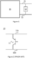
- An exemplary configuration is shown in Figure 1 , in which an ESD protection device 10 is connected in between, for example, a signal line 21 and a rail line 22 of an electronic circuit 20, such as an integrated circuit (IC).
- ESD protection device 10 can be integrated with electronic circuit 20 into a single IC.
- the ESD protection device or circuit has a relatively high current handling capability, and prevents or limits a current due to an ESD event from flowing through the sensitive electronic device(s) by allowing a substantial portion of said current to flow through the ESD protection device instead.
- the ESD protection device should limit the voltages within the sensitive electronic device(s) or circuit(s) to sufficiently low levels to prevent damage to connected electronic device(s) or circuit(s) to be protected.
- a bipolar junction transistor (BJT) in an open-base configuration is frequently used in ESD protection devices.
- the open-base configuration refers to the BJT being operated as a two-terminal device by leaving the base terminal of the BJT unconnected. Consequently, in operation, the base terminal of the BJT will be at a floating potential.
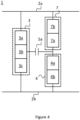
- a BJT 11 in open-base configuration is connected in between a first terminal 12a and a second terminal 12b.
- First and second terminal 12a, 12b may for example correspond to terminals of ESD protection device 10 as shown in Figure 1 .
- BJT 11 may be formed either symmetrically or asymmetrically.
- the emitter and collector region thereof are identically or similarly doped such that BJT 11 operates substantially identically irrespective of the polarity of the ESD event.
- the emitter of BJT 11 may assume the role of the collector, and vice versa, depending on the polarity of the ESD event.
- a performance of ESD protection device 10 may differ depending on the polarity of the ESD event.
- ESD protection device 10 The operation of ESD protection device 10 is as follows. During an ESD event, a voltage across first and second terminal 12a, 12b rises rapidly. Since the base terminal of BJT 11 is at a floating potential, its electrical potential will self-adjust during the ESD event. In particular, during an ESD event, the base-collector junction of BJT 11 will be reverse-biased, such that initially substantially no current can flow through BJT 11. Therefore, the base-emitter junction also cannot be forward-biased at this stage. This condition is ensured by the self-adjusting electrical potential of the base. In other words, as the voltage across the first and second terminal 12a, 12b increases (i.e., due to the ESD event), the voltage across the base-collector junction will also increase.
- the voltage across the base-collector junction will exceed a breakdown voltage of said junction, resulting in an avalanche breakdown of said junction. Since a current can now flow through the base-collector junction, the base-emitter junction will become forward-biased due to the self-adjusting electrical potential of the base, thereby enabling a current flow between first and second device terminal 12a, 12b through BJT 11. At this point, the emitter of BJT 11 starts injecting charge carriers into the base. Once the charge carriers from the emitter reach the base-collector avalanche region, BJT 11 will enter a 'snapback' mode, and the voltage across BJT 11 will decrease. At this point, BJT 11 switches to a low-Ohmic on-state, in which state a substantial current from the ESD event can be accommodated.
- a problem associated with the known ESD protection device is that the open-base BJT may not switch sufficiently quickly into its low-Ohmic on-state to prevent damages to the electronic circuit to be protected. Prior to the BJT being in its low-Ohmic on-state, the potential difference across the terminals of the ESD protection device due to the ESD event may be substantial and may cause significant and/or permanent damage to the electronic circuit to be protected.
- the turn-on time of the known ESD protection device may be particularly slow when using low-capacitance BJTs having a relatively large and lowly doped base region. This is because a substantial number of charge carriers must be injected from the emitter into the relatively large base before the BJT can switch to its low-Ohmic on-state.
- BJT low-capacitance BJTs having a relatively large and lowly doped base region.
- a substantial number of charge carriers must be injected from the emitter into the relatively large base before the BJT can switch to its low-Ohmic on-state.
- using a BJT with a higher associated capacitance is not preferred, as this would increase the capacitive loading of the ESD protection device on the electronic circuit to be protected, which may adversely affect the performance of said electronic circuit.
- the semiconductor device has a first device terminal and a second device terminal, and comprises a semiconductor body having a first electronic component integrated thereon.
- the first electronic component comprises a first primary region of a first charge type electrically connected to the first device terminal, a second primary region of a second charge type arranged adjacent to the first primary region, and a third primary region of the first charge type arranged adjacent to the second primary region and being electrically connected to the second device terminal.
- the semiconductor device according to the present invention is characterized in that it further comprises a second electronic component integrated on the semiconductor body and being spaced apart from the first electronic component, the second electronic component comprising a first secondary region of the first charge type and a second secondary region of the second charge type arranged adjacent to the first secondary region, wherein the second secondary region is electrically connected to the second device terminal. Furthermore, the semiconductor device according to the present invention comprises a first capacitive element, a first terminal thereof being electrically connected to the second primary region, and a second terminal thereof being electrically connected to the first secondary region.
- the first electronic component as described above may form a BJT, and the second electronic component may form a diode.
- the turn-on time of the open-base BJT known in the art can at least partially be attributed to the fact that the emitter is only able to inject charge carriers into the base once avalanche breakdown of the base-collector junction is initiated. This is because the base-emitter junction cannot be forward-biased until a current flow through the BJT, due to avalanche breakdown at the base-collector junction, is possible. In other words, a two-step process is required to enable the BJT to switch into its low-Ohmic on-state. First, a certain amount of time is required to build up a potential difference across the base-collector junction and thereby initiate avalanche breakdown at the base-collector junction. Subsequently, a certain amount of time is needed to inject charge carriers from the emitter into the base of the BJT.
- the first capacitive element in combination with the second electronic component according to the present invention enables a current flow through the junction between the first primary region and the second primary region, even though no avalanche breakdown is initiated at the junction between the second primary region and the third primary region. With this current flow, charge carriers are injected from the first primary region (e.g., the emitter) into the second primary region (e.g., the base) before avalanche breakdown occurs in the first electronic component. Furthermore, the first capacitive element ensures that the second primary region and the first secondary region are at a floating potential.
- the electrical potential across the first and second device terminal rises rapidly. During this voltage rise, the floating electrical potential of the second primary region and the first secondary region will self-adjust. After some time, the voltage across the junction between the first primary region and the second primary region, as well as the voltage across the junction between the first secondary region and the second secondary region, will be sufficient to forward-bias said junctions. This enables a current flow from one of the first and second device terminal to the other through said junctions and through the first capacitive element.
- the second primary region can be at least partially filled with charge carriers already prior to the avalanche breakdown.
- the first electronic component can switch to its low-Ohmic on-state significantly faster with respect to a conventional open-base BJT.
- the first electronic component can enter the snapback mode substantially immediately after avalanche breakdown is initiated, thus significantly reducing the turn-on time.
- the first electronic component is able to accommodate the sudden discharge current from the ESD event to thereby protect the electronic circuit to which it is connected.
- the second primary region is filled with charge carriers at an earlier moment during the ESD event, a peak or 'overshoot' voltage due to said ESD event is reduced compared to the conventional open-base BJT.
- the semiconductor device according to the present invention also protects an electronic circuit from excessive voltage levels due to the ESD event.
- the amount of charge that the first capacitive element is able to store is proportional to its capacitance value.
- the first capacitive element may have a large enough capacitance such that the charge that can be stored on the first capacitive element can be made equal to or greater than the charge required to substantially fill the second primary region.
- the snapback effect occurs substantially immediately after avalanche breakdown occurs, such that the first electronic component enters its low-Ohmic on-state.
- the turn-on time of the first electronic component is also reduced for smaller capacitance values.
- the turn-on time of the first electronic component is still reduced, since the number of charge carriers that must be injected after avalanche breakdown occurs is reduced.
- the junction between the first secondary region and the second secondary region is not forward-biased. Consequently, the associated junction capacitance thereof is relatively small. Since the first capacitive element is connected in series with the second electronic component comprising said first and second secondary region, the combined effective capacitance value may be dominated by this junction capacitance during normal operation, such that the capacitive loading of the semiconductor device on the electronic circuit to be protected is reduced during normal operation.
- the semiconductor device according to the present invention as described above provides a faster turn-on time only in one direction, and the directionality depends on the selected dopant type for the first and second charge type. For example, if the first charge type is p-type and the second charge type is n-type, the turn-on time is improved for a voltage rise at the first device terminal with respect to the second device terminal. On the other hand, if the first charge type is n-type and the second charge type is p-type, the turn-on time is improved for a voltage rise at the second device terminal with respect to the first device terminal.
- the semiconductor device may further comprise a third electronic component integrated on the semiconductor body and being spaced apart from the first electronic component and the second electronic component.
- the third electronic component may comprise a first tertiary region of the first charge type and a second tertiary region of the second charge type arranged adjacent to the first tertiary region.
- the second tertiary region may be electrically connected to the first device terminal.
- the third electronic component may for example form a diode.
- the first tertiary region may be electrically connected to the second terminal of the first capacitive element.
- the semiconductor device may further comprise a further first capacitive element having a first terminal thereof electrically connected to the second primary region and having a second terminal thereof electrically connected to the first tertiary region.
- the second electronic component in combination with the first capacitive element enables the first electronic component to have a faster turn-on time in one direction (i.e., for a particular ESD event polarity), while the third electronic component in combination with the first capacitive element enables a faster turn-on time of the first electronic component in the other direction.
- the second electronic component may further comprise a third secondary region of the second charge type arranged adjacent to the first secondary region, wherein the third secondary region is electrically connected to the first device terminal.
- the second electronic component may for example form a BJT.
- junction between the first secondary region and the second secondary region effectively forms a diode for enabling a faster turn-on time of the first electronic component in one particular direction
- junction between the first secondary region and the third secondary region effectively forms a diode for enabling a faster turn-on time of the first electronic component in the other direction
- junction between the first primary region and the second primary region effectively forms a diode for enabling a faster turn-on time of the second electronic component in one particular direction
- the junction between the second primary region and the third primary region effectively forms a diode for enabling a faster turn-on time of the second electronic component in the other direction.
- a current can flow through part of the first and second electronic component via the first capacitive element, thereby injecting charge carriers into the second primary region and the first secondary region (e.g., the base regions) of the first and second electronic component, respectively, even though avalanche breakdown in the first and second electronic component did not yet occur.
- the second primary region may comprise a first primary sub-region arranged adjacent to the first primary region, and a second primary sub-region arranged in between said first primary sub-region and the third primary region.
- a dopant concentration of the first primary sub-region may be less than that of the second primary sub-region, the first primary region and the third primary region.
- the first secondary region may comprise a first secondary sub-region arranged adjacent to the third secondary region, and a second secondary sub-region arranged in between said first secondary sub-region and the second secondary region.
- a dopant concentration of the first secondary sub-region may be less than that of the second secondary sub-region, the second secondary region and the third secondary region.
- the first capacitive element may be electrically connected between at least one of the first and second primary sub-region and at least one of the first and second secondary sub-region.
- the junction between the first primary region and the first primary sub-region will have a relatively low associated capacitance value, while the junction between the second primary sub-region and the third primary region will have a relatively low associated breakdown voltage.
- the junction between the third secondary region and the first secondary sub-region will have a relatively low associated capacitance value, while the junction between the second secondary sub-region and the second secondary region will have a low associated breakdown voltage.
- the first electronic component and the second electronic component are asymmetrical. Consequently, during an ESD event, due to the difference in breakdown voltage of respective junctions of the first and second electronic component, one of the first electronic component and the second electronic component will switch to its low-Ohmic on-state first, depending on the polarity of the ESD event and on the selected dopant type for the first and second charge type.
- the first charge type may be n-type
- the second charge type may be p-type.
- the ESD current may flow substantially only through the first electronic component after turn-on.
- the other of the first and second electronic component may switch later, or may not switch at all, depending on the selected dopant concentrations for the various regions of the first and second electronic component. For example, after the first electronic component turns on, the voltage across the junction between the first and third secondary region may not be large enough for avalanche breakdown to occur at said junction. In that case, the second electronic component may not turn on during the same ESD event.
- the second primary region may further comprise a third primary sub-region arranged in between the second primary sub-region and the third primary region.
- a dopant concentration of the third primary sub-region may be less than that of the second primary sub-region and the third primary region.
- the first secondary region may further comprise a third secondary sub-region arranged in between the second secondary sub-region and the second secondary region.
- a dopant concentration of the third secondary sub-region may be less than that of the second secondary sub-region and the second secondary region.
- Having a highly doped region arranged in between lowly doped regions in the second primary region and/or the first secondary region prevents or at least limits the occurrence of punch-through during operation.
- the depletion region in the second primary region and/or the first secondary region may not extend across the said region due to the highly doped region.
- a junction capacitance between, for example, the first and second primary region and between the second and third primary region is smaller due to lowly doped regions in said second primary region being adjacent to said first and third primary region, respectively.
- the first electronic component may further comprise a fourth primary region of the second charge type arranged adjacent to the third primary region, wherein the third primary region is electrically connected to the second device terminal through the fourth primary region.
- the semiconductor device may further comprise a second capacitive element, a first terminal thereof being electrically connected to the third primary region, and a second terminal thereof being electrically connected to the second secondary region.
- the second secondary region may be electrically connected to the second device terminal through the second capacitive element, the third primary region and the fourth primary region.
- the first electronic component may for example form a thyristor or a silicon controlled rectifier, SCR.
- the semiconductor device may comprise a first resistor electrically connected between the first device terminal and the second primary region, and/or a second resistor electrically connected between the second device terminal and the third primary region.
- each of the second primary region, the third primary region, the first secondary region and the second secondary region are at a floating electrical potential.
- a current path between the first and second device terminal is obtained through said junctions and through the first and second capacitive element.
- Charge carriers are then injected from the first primary region into the second primary region, and from the fourth primary region into the third primary region, even though avalanche breakdown has not yet occurred at the junction between the second primary region and the third primary region.
- the second primary region and the third primary region can be substantially filled with charge carriers already prior to the avalanche breakdown.
- the first electronic component can then switch to its low-Ohmic on-state once the avalanche breakdown occurs.
- the second electronic component may further comprise a third secondary region of the second charge type arranged adjacent to the first secondary region.
- the third secondary region may be electrically connected to the first device terminal.
- the second electronic component may further comprise a fourth secondary region of the first charge type arranged adjacent to the second secondary region.
- the fourth secondary region may be electrically connected to the second device terminal.
- the second electronic component may for example form a BJT. If the second electronic component comprises both the third secondary region and the fourth secondary region, then the second electronic component may for example form a thyristor or SCR. In the latter case, the semiconductor device may further comprise a third resistor electrically connected between the first device terminal and the first secondary region, and/or a fourth resistor electrically connected between the second device terminal and the second secondary region.
- the semiconductor device will exhibit a reduced turn-on time irrespective of the polarity of the ESD event.
- the ESD current will flow through one of the first and second electronic component depending on the polarity of the ESD event and the selected dopant type for the first and second charge type. For example, if the first charge type is p-type and the second charge type is n-type, then the ESD current will flow through the first electronic component, which will be in a low-Ohmic state after being turned on. On the other hand, if the first charge type is n-type and the second charge type is p-type, the ESD current will flow through the second electronic component, which will be in a low-Ohmic state after being turned on.
- the semiconductor body may comprise a semiconductor substrate and an epitaxial layer on top of said semiconductor substrate.
- the first electronic component, the second electronic component and, if applicable, the third electronic component may be arranged in the epitaxial layer of the semiconductor body.
- the first charge type may correspond to a p-type or n-type doping
- the second charge type may correspond to an n-type or p-type doping, respectively.
- respective regions corresponding to the first electronic component, the second electronic component and/or, if applicable, the third electronic component may be ion-implanted regions.
- the semiconductor body may be based on one of silicon, Si, silicon carbide, SiC, gallium nitride, GaN, and gallium arsenide, GaAs, technology.
- the first capacitive element and/or, if applicable, the further first capacitive element and/or the second capacitive element may comprise a metal oxide semiconductor, MOS, capacitor.
- a dopant concentration of the first and third primary region, and of the second and third secondary region may lie in the range between 1e18 - 1e20, and a dopant concentration of the second primary region and the first secondary region may lie in the range between 1e15 - 1e18.
- a dopant concentration of the first primary and/or secondary sub-region may lie in the range between 1e13 - 1e16, and a dopant concentration of the second primary and/or secondary sub-region may lie in the range between 1e15 - 1e18.
- the present invention is not limited to these dopant concentration ranges, and adjustments can be made accordingly.
- the semiconductor device may comprise metal contact elements, such as those formed in a metal layer on top of the semiconductor body, for electrically contacting one or more respective regions of the first and second electronic component and providing external electrical access to said regions.
- metal contact elements such as those formed in a metal layer on top of the semiconductor body, for electrically contacting one or more respective regions of the first and second electronic component and providing external electrical access to said regions.
- a low-Ohmic contact between various regions of the first and second electronic component and such a metal connection element may be provided by providing said regions with a highly doped contact sub-region adjacent to said metal connections, as will be appreciated by those skilled in the art.
- the highly doped contact sub-region may for example have a dopant concentration in a range of 1e18 - 1e20.
- an ESD protection device configured to be electrically connected to an electronic circuit and to protect said electronic circuit from ESD events.
- the ESD protection device comprises one or more semiconductor devices according to the present invention as defined above, and is preferably a packaged device.
- a device that comprises an electronic circuit integrated on a semiconductor body, and one or more semiconductor devices according to the present invention as defined above.
- the one or more semiconductor devices are integrated in the semiconductor body and are connected to the electronic circuit to protect said electronic circuit from ESD events.
- the device is a packaged device.
- semiconductor device 1 comprises a first electronic component 3, a second electronic component 4, and a first capacitive element 5a connected in between said first electronic component 3 and second electronic component 4.
- first electronic component 3 comprises a first primary region 3a of a first charge type (e.g., p-type), a second primary region 3b of a second charge type (e.g., n-type) and a third primary region 3c of the first charge type.
- Second electronic component 4 comprises a first secondary region 4a of the first charge type and a second secondary region 4b of the second charge type.
- first capacitive element 5a is connected in between second primary region 3b and first secondary region 4a.
- First primary region 3a is electrically connected to a first device terminal 2a of semiconductor device 1, while third primary region 3c and second secondary region 4b are electrically connected to a second device terminal 2b of semiconductor device 1.
- first electronic component 3 forms a BJT
- second electronic component 4 forms a diode.
- the first charge type may correspond to a p-type or n-type doping
- the second charge type may correspond to an n-type or p-type doping, respectively.
- the first charge type corresponds to a p-type doping
- the second charge type corresponds to an n-type doping.
- first electronic component 3 when an ESD event occurs, a potential difference across first and second device terminal 2a, 2b may increase.
- first electronic component 3 In order to prevent substantial damages to an electronic circuit to which semiconductor device 1 is connected, first electronic component 3 must be activated such that the ESD current can be discharged through first electronic component 3.
- an overvoltage resulting from the ESD event should be limited to protect said electronic circuit from being exposed to excessive voltage levels.
- Second primary region 3b and first secondary region 4a are at a floating potential. Therefore, when the voltage at first device terminal 2a increases due to an ESD event, the electrical potential at second primary region 3b and first secondary region 4a will self-adjust until the junction between first and second primary region 3a, 3b and the junction between first and second secondary region 4a, 4b are both forward-biased. At this moment, a current will flow from first device terminal 2a to second device terminal 2b through said junctions and through first capacitive element 5a. Due to this current flow, charge carriers (i.e., holes) are injected from the p-type first primary region 3a into the n-type second primary region 3b, thereby filling second primary region 3b with charge carriers.
- charge carriers i.e., holes
- the electrical potential at second primary region 3b will continue increasing as the voltage at first device terminal 2a rises. After some time, a voltage across the junction between second and third primary region 3b, 3c will exceed a breakdown voltage of said junction, resulting in an avalanche breakdown occurring at said junction.
- the avalanche breakdown at this junction enables a current to flow from first device terminal 2a to second device terminal 2b through primary regions 3a-3c of first electronic component 3.
- second primary region 3b is already substantially filled with charge carriers at this stage, once the avalanche breakdown is initiated, the snapback effect will occur substantially immediately, and first electronic component 3 switches to its low-Ohmic on-state.
- first electronic component 3 has the current handling capability to discharge the current resulting from the ESD event, thereby preventing or substantially limiting said current from flowing through the electronic circuit that is to be protected.
- first electronic component 3 since first electronic component 3 switches to its on-state soon after avalanche breakdown occurs, the overvoltage at first device terminal 2a is substantially limited.
- Figure 3B illustrates an exemplary cross-sectional view of semiconductor device 1. More in particular, Figure 3B shows primary regions 3a-3c of first electronic component 3 and secondary regions 4a, 4b of second electronic component 4 arranged in a semiconductor body 6.
- semiconductor body 6 may comprise a semiconductor substrate having an epitaxial layer grown thereon, and the various regions of semiconductor device 1 may be arranged in the epitaxial layer.
- First capacitive element 5a may be implemented in various ways.
- first capacitive element 5a may be formed using one or more metal-oxide-semiconductor (MOS) capacitors.
- MOS metal-oxide-semiconductor
- a metal layer stacked on top of an oxide layer may be arranged on a surface portion of semiconductor body 6 above second primary region 3b and first secondary region 4a semiconductor body 6.
- First capacitive element 5a may for example instead be a discrete capacitor that is mounted on semiconductor body 6 and electrically connected in between second primary region 3b and first secondary region 4a.
- first device terminal 2a and second device terminal 2b may for example be formed using metal connections arranged in a metal layer on top of semiconductor body 6.
- embodiments of semiconductor device 1 shown in Figures 4-9 may be formed in a manner similar to the structure shown in Figure 3B , as will be appreciated by those skilled in the art. A cross-sectional view and a corresponding detailed description thereof may therefore be omitted.
- FIG 4 illustrates another embodiment of semiconductor device 1 according to the present invention.
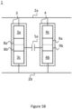
- Semiconductor device 1 in Figure 4 differs from that in Figure 3 in that the device further comprises a third electronic component 7, comprising a first tertiary region 7a of the first charge type and a second tertiary region 7b of the second charge type.
- second electronic component 4 in combination with first capacitive element 5a are included to improve a turn-on time of first electronic component 3 for one particular ESD event polarity.
- first charge type is p-type and the second charge type is n-type
- the improved turn-on time of first electronic component 3 occurs for a voltage increase at first device terminal 2a.
- third electronic component 7, as shown in Figure 4 can be included to improve the turn-on time of first electronic component 3 for an opposite ESD polarity, i.e., a voltage increase at second device terminal 2b.
- first capacitive element 5a is shown to be connected to both first secondary region 4a and first tertiary region 7a.
- first capacitive element 5a may be only connected between second primary region 3b and first secondary region 4a, and semiconductor device 1 may further comprise a further first capacitive element (not shown) that is connected between second primary region 3b and first tertiary region 7a.
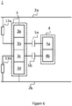
- FIG 5A another embodiment of semiconductor device 1 is shown.
- third electronic component 7 is not included, and second electronic component 4 further comprises a third secondary region 4c of the second charge type.
- both first electronic component 3 and second electronic component 4 may form a BJT.
- semiconductor device 1 shown in Figure 5A is similar to that of semiconductor device 1 shown in Figure 4 .
- a current path between first and second device terminal 2a, 2b is provided through the PN-junction between first and second primary regions 3a, 3b, first capacitive element 5a, and the PN-junction between first and second secondary regions 4a, 4b.
- This current flow allows charge carriers to be injected into second primary region 3b and into first secondary region 4a.
- both first electronic component 3 and second electronic component 4 will enter their respective low-Ohmic on-state. Consequently, the current resulting from the ESD event can be discharged through first electronic component 3 and through second electronic component 4.
- second primary region 3b and first secondary region 4a of semiconductor device 1 shown in Figure 5A are divided into a plurality of sub-regions.
- second primary region 3b is divided into a first primary sub-region 8a and a second primary sub-region 8b
- first secondary region 4a is divided into a first secondary sub-region 9a and a second secondary sub-region 9b.
- a dopant concentration of first primary sub-region 8a is less than a dopant concentration of second primary sub-region 8b and first primary region 3a.
- the PN-junction between first primary region 3a and first primary sub-region 8a has a relatively low associated capacitance value, while the PN-junction between second primary sub-region 8b and third primary region 3c has a relatively low breakdown voltage.
- a dopant concentration of first secondary sub-region 9a is less than a dopant concentration of second secondary sub-region 9b and third secondary region 4c.
- the PN-junction between third secondary region 4c and first secondary sub-region 9a has a relatively low associated capacitance value, while the PN-junction between second secondary sub-region 9b and second secondary region 4b has a relatively low breakdown voltage.
- second primary region 3b further comprises a third primary sub-region 8c
- first secondary region 4a further comprises a third secondary sub-region 8c.
- a dopant concentration of third primary sub-region 8c is less than the dopant concentration of second primary sub-region 8b and third primary region 3c, and may be similar or equal to the dopant concentration of first primary sub-region 8a.
- a dopant concentration of third secondary sub-region 9c is less than the dopant concentration of second secondary sub-region 9b and second secondary region 4b, and may be similar or equal to the dopant concentration of first secondary sub-region 9a.
- Each junction in first electronic component 3 and second electronic component 4 will then have a lower associated capacitance value.
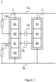
- first electronic component 3 comprises a fourth primary region 3d of the second charge type that is electrically connected to second device terminal 2b.
- semiconductor 1 further comprises a second capacitive element 5b connected between third primary region 3c and second secondary region 4b.
- Second secondary region 4b is not directly electrically connected to second device terminal 2b, but is instead electrically connected thereto through second capacitive element 5b, third primary region 3c and fourth primary region 3d.
- first electronic component 3 forms a thyristor or SCR.
- Semiconductor 1 optionally comprises at least one of a first resistor 13a electrically connected between first device terminal 2a and second primary region 3b, and a second resistor 13b electrically connected between second device terminal 2b and third primary region 3c.
- a current path is provided from first device terminal 2a to second device terminal 2b when each of the junctions between first and second primary region 3a, 3b, first and second secondary region 4a, 4b, and third and fourth primary region 3c, 3d become forward-biased.
- charge carriers are injected into the second and third primary region 3b, 3c.
- holes are injected from first primary region 3a into second primary region 3b, and electrons are injected from fourth primary region 3d into third primary region 3c.
- first electronic component 3 switches to its low-Ohmic on-state and discharges the ESD current.
- first electronic component 3 forms a thyristor or SCR
- second electronic component 4 forms a BJT.
- second electronic component 4 comprises a third secondary region 4c, as shown in Figure 7 , or a fourth secondary region 4d, as shown in Figure 8 .
- an operation of semiconductor device 1 for a voltage rise at first device terminal 2a may be similar to that of the device shown in Figure 6 .
- the operation of semiconductor device 1 may be similar to that of the device shown in Figure 3 .
- both first electronic component 3 and second electronic component 4 of semiconductor device 1 form a thyristor or SCR.
- second electronic component comprises both third secondary region 4c and fourth secondary region 4d.
- semiconductor 1 optionally comprises at least one of a third resistor 14a electrically connected between first device terminal 2a and first secondary region 4a, and a fourth resistor 14b electrically connected between second device terminal 2b and second secondary region 4b.
- first electronic component 3 will switch to its low-Ohmic on-state after avalanche breakdown occurs at the junction between second and third primary region 3b, 3c occurs.
- second electronic component 4 will switch to its low-Ohmic on-state after avalanche breakdown occurs at the junction between first and second secondary region 4a, 4b.
Landscapes
- Semiconductor Integrated Circuits (AREA)
Abstract
Description
- The present invention relates to a semiconductor device. More in particular, the present invention relates to a semiconductor device that is particularly useful for ESD protection purposes.
- Electronic devices and circuits may be subject to electrostatic discharge (ESD) events, for example due to close contact between said device (or circuit) with a differently-charged object, or due to a breakdown of a dielectric between said device (or circuit) and said object, resulting in a sudden flow of electricity. Excessive currents due to a sudden discharge from an ESD event can cause significant and/or permanent damage to sensitive electronic devices.
- ESD protection devices can be used to prevent such damage to electronic devices or circuits. For example, a dedicated ESD protection device can be electrically connected in parallel to the electronic device to shunt the ESD current. An exemplary configuration is shown in
Figure 1 , in which anESD protection device 10 is connected in between, for example, asignal line 21 and arail line 22 of anelectronic circuit 20, such as an integrated circuit (IC). Alternatively,ESD protection device 10 can be integrated withelectronic circuit 20 into a single IC. - Generally, the ESD protection device or circuit has a relatively high current handling capability, and prevents or limits a current due to an ESD event from flowing through the sensitive electronic device(s) by allowing a substantial portion of said current to flow through the ESD protection device instead. At the same time, the ESD protection device should limit the voltages within the sensitive electronic device(s) or circuit(s) to sufficiently low levels to prevent damage to connected electronic device(s) or circuit(s) to be protected.
- A bipolar junction transistor (BJT) in an open-base configuration, such as shown in
Figure 2 , is frequently used in ESD protection devices. Here, the open-base configuration refers to the BJT being operated as a two-terminal device by leaving the base terminal of the BJT unconnected. Consequently, in operation, the base terminal of the BJT will be at a floating potential. - In
Figure 2 , aBJT 11 in open-base configuration is connected in between afirst terminal 12a and asecond terminal 12b. First andsecond terminal ESD protection device 10 as shown inFigure 1 . - BJT 11 may be formed either symmetrically or asymmetrically. For a
symmetrical BJT 11, the emitter and collector region thereof are identically or similarly doped such that BJT 11 operates substantially identically irrespective of the polarity of the ESD event. In that case, the emitter ofBJT 11 may assume the role of the collector, and vice versa, depending on the polarity of the ESD event. Alternatively, if BJT 11 is formed asymmetrically, a performance ofESD protection device 10 may differ depending on the polarity of the ESD event. - The operation of
ESD protection device 10 is as follows. During an ESD event, a voltage across first andsecond terminal BJT 11. Therefore, the base-emitter junction also cannot be forward-biased at this stage. This condition is ensured by the self-adjusting electrical potential of the base. In other words, as the voltage across the first andsecond terminal - After some time, the voltage across the base-collector junction will exceed a breakdown voltage of said junction, resulting in an avalanche breakdown of said junction. Since a current can now flow through the base-collector junction, the base-emitter junction will become forward-biased due to the self-adjusting electrical potential of the base, thereby enabling a current flow between first and
second device terminal BJT 11. At this point, the emitter of BJT 11 starts injecting charge carriers into the base. Once the charge carriers from the emitter reach the base-collector avalanche region, BJT 11 will enter a 'snapback' mode, and the voltage acrossBJT 11 will decrease. At this point, BJT 11 switches to a low-Ohmic on-state, in which state a substantial current from the ESD event can be accommodated. - A problem associated with the known ESD protection device is that the open-base BJT may not switch sufficiently quickly into its low-Ohmic on-state to prevent damages to the electronic circuit to be protected. Prior to the BJT being in its low-Ohmic on-state, the potential difference across the terminals of the ESD protection device due to the ESD event may be substantial and may cause significant and/or permanent damage to the electronic circuit to be protected.
- The turn-on time of the known ESD protection device may be particularly slow when using low-capacitance BJTs having a relatively large and lowly doped base region. This is because a substantial number of charge carriers must be injected from the emitter into the relatively large base before the BJT can switch to its low-Ohmic on-state. On the other hand, using a BJT with a higher associated capacitance is not preferred, as this would increase the capacitive loading of the ESD protection device on the electronic circuit to be protected, which may adversely affect the performance of said electronic circuit.
- It is an object of the present invention to provide a semiconductor device for which the abovementioned problems are prevented or limited.
- This object is achieved with the semiconductor device according to
claim 1. The semiconductor device has a first device terminal and a second device terminal, and comprises a semiconductor body having a first electronic component integrated thereon. The first electronic component comprises a first primary region of a first charge type electrically connected to the first device terminal, a second primary region of a second charge type arranged adjacent to the first primary region, and a third primary region of the first charge type arranged adjacent to the second primary region and being electrically connected to the second device terminal. - The semiconductor device according to the present invention is characterized in that it further comprises a second electronic component integrated on the semiconductor body and being spaced apart from the first electronic component, the second electronic component comprising a first secondary region of the first charge type and a second secondary region of the second charge type arranged adjacent to the first secondary region, wherein the second secondary region is electrically connected to the second device terminal. Furthermore, the semiconductor device according to the present invention comprises a first capacitive element, a first terminal thereof being electrically connected to the second primary region, and a second terminal thereof being electrically connected to the first secondary region.
- The first electronic component as described above may form a BJT, and the second electronic component may form a diode.
- The turn-on time of the open-base BJT known in the art can at least partially be attributed to the fact that the emitter is only able to inject charge carriers into the base once avalanche breakdown of the base-collector junction is initiated. This is because the base-emitter junction cannot be forward-biased until a current flow through the BJT, due to avalanche breakdown at the base-collector junction, is possible. In other words, a two-step process is required to enable the BJT to switch into its low-Ohmic on-state. First, a certain amount of time is required to build up a potential difference across the base-collector junction and thereby initiate avalanche breakdown at the base-collector junction. Subsequently, a certain amount of time is needed to inject charge carriers from the emitter into the base of the BJT.
- The first capacitive element in combination with the second electronic component according to the present invention enables a current flow through the junction between the first primary region and the second primary region, even though no avalanche breakdown is initiated at the junction between the second primary region and the third primary region. With this current flow, charge carriers are injected from the first primary region (e.g., the emitter) into the second primary region (e.g., the base) before avalanche breakdown occurs in the first electronic component. Furthermore, the first capacitive element ensures that the second primary region and the first secondary region are at a floating potential.
- Prior to an ESD event, none of the junctions between adjacent regions of the semiconductor device are forward-biased. The second primary region and the first secondary region, between which the first capacitive element is coupled, are both at a floating potential. Consequently, the electrical potential at said regions will be self-adjusting.
- During an ESD event, the electrical potential across the first and second device terminal rises rapidly. During this voltage rise, the floating electrical potential of the second primary region and the first secondary region will self-adjust. After some time, the voltage across the junction between the first primary region and the second primary region, as well as the voltage across the junction between the first secondary region and the second secondary region, will be sufficient to forward-bias said junctions. This enables a current flow from one of the first and second device terminal to the other through said junctions and through the first capacitive element.
- With the current flow via the first capacitive element, charge carriers are injected into the second primary region and the first secondary region even before avalanche breakdown at the junction between the second primary region and the third primary region occurs. In other words, the second primary region can be at least partially filled with charge carriers already prior to the avalanche breakdown. Once the voltage across the junction between the second primary region and the third primary region exceeds the breakdown voltage, the first electronic component can switch to its low-Ohmic on-state significantly faster with respect to a conventional open-base BJT. In particular, if the second primary region is already substantially filled with charge carriers prior to the avalanche breakdown, then the first electronic component can enter the snapback mode substantially immediately after avalanche breakdown is initiated, thus significantly reducing the turn-on time. In the low-Ohmic on-state, the first electronic component is able to accommodate the sudden discharge current from the ESD event to thereby protect the electronic circuit to which it is connected. In addition, since the second primary region is filled with charge carriers at an earlier moment during the ESD event, a peak or 'overshoot' voltage due to said ESD event is reduced compared to the conventional open-base BJT. As a result, the semiconductor device according to the present invention also protects an electronic circuit from excessive voltage levels due to the ESD event.
- The amount of charge that the first capacitive element is able to store is proportional to its capacitance value. In order to substantially fill the second primary region with charge carriers, the first capacitive element may have a large enough capacitance such that the charge that can be stored on the first capacitive element can be made equal to or greater than the charge required to substantially fill the second primary region.
- If the second primary region is already substantially filled with charge carriers prior to the avalanche breakdown, the snapback effect occurs substantially immediately after avalanche breakdown occurs, such that the first electronic component enters its low-Ohmic on-state. However, it will be appreciated by a person skilled in the art that the turn-on time of the first electronic component is also reduced for smaller capacitance values. In particular, even if the second primary region is not substantially filled with charge carriers prior to avalanche breakdown, the turn-on time of the first electronic component is still reduced, since the number of charge carriers that must be injected after avalanche breakdown occurs is reduced.
- During normal operation of the electronic circuit to be protected, the junction between the first secondary region and the second secondary region is not forward-biased. Consequently, the associated junction capacitance thereof is relatively small. Since the first capacitive element is connected in series with the second electronic component comprising said first and second secondary region, the combined effective capacitance value may be dominated by this junction capacitance during normal operation, such that the capacitive loading of the semiconductor device on the electronic circuit to be protected is reduced during normal operation.
- The semiconductor device according to the present invention as described above provides a faster turn-on time only in one direction, and the directionality depends on the selected dopant type for the first and second charge type. For example, if the first charge type is p-type and the second charge type is n-type, the turn-on time is improved for a voltage rise at the first device terminal with respect to the second device terminal. On the other hand, if the first charge type is n-type and the second charge type is p-type, the turn-on time is improved for a voltage rise at the second device terminal with respect to the first device terminal.
- However, a bidirectional semiconductor device is also envisaged. To this end, the semiconductor device may further comprise a third electronic component integrated on the semiconductor body and being spaced apart from the first electronic component and the second electronic component. The third electronic component may comprise a first tertiary region of the first charge type and a second tertiary region of the second charge type arranged adjacent to the first tertiary region. The second tertiary region may be electrically connected to the first device terminal. The third electronic component may for example form a diode.
- Furthermore, the first tertiary region may be electrically connected to the second terminal of the first capacitive element. Alternatively, the semiconductor device may further comprise a further first capacitive element having a first terminal thereof electrically connected to the second primary region and having a second terminal thereof electrically connected to the first tertiary region.
- In the above embodiment, the second electronic component in combination with the first capacitive element enables the first electronic component to have a faster turn-on time in one direction (i.e., for a particular ESD event polarity), while the third electronic component in combination with the first capacitive element enables a faster turn-on time of the first electronic component in the other direction.
- Instead of including a third electronic component to obtain a bidirectional semiconductor device, the second electronic component may further comprise a third secondary region of the second charge type arranged adjacent to the first secondary region, wherein the third secondary region is electrically connected to the first device terminal. The second electronic component may for example form a BJT.
- The junction between the first secondary region and the second secondary region effectively forms a diode for enabling a faster turn-on time of the first electronic component in one particular direction, while the junction between the first secondary region and the third secondary region effectively forms a diode for enabling a faster turn-on time of the first electronic component in the other direction. Furthermore, the junction between the first primary region and the second primary region effectively forms a diode for enabling a faster turn-on time of the second electronic component in one particular direction, and the junction between the second primary region and the third primary region effectively forms a diode for enabling a faster turn-on time of the second electronic component in the other direction. This enables a symmetric operation in which both the first electronic component and the second electronic component switch to a low-Ohmic on-state after the snapback effect occurs for the respective electronic components, regardless of the polarity of the ESD event. More in particular, a current can flow through part of the first and second electronic component via the first capacitive element, thereby injecting charge carriers into the second primary region and the first secondary region (e.g., the base regions) of the first and second electronic component, respectively, even though avalanche breakdown in the first and second electronic component did not yet occur.
- The second primary region may comprise a first primary sub-region arranged adjacent to the first primary region, and a second primary sub-region arranged in between said first primary sub-region and the third primary region. A dopant concentration of the first primary sub-region may be less than that of the second primary sub-region, the first primary region and the third primary region. Furthermore, the first secondary region may comprise a first secondary sub-region arranged adjacent to the third secondary region, and a second secondary sub-region arranged in between said first secondary sub-region and the second secondary region. A dopant concentration of the first secondary sub-region may be less than that of the second secondary sub-region, the second secondary region and the third secondary region. The first capacitive element may be electrically connected between at least one of the first and second primary sub-region and at least one of the first and second secondary sub-region.
- In the above embodiment, the junction between the first primary region and the first primary sub-region will have a relatively low associated capacitance value, while the junction between the second primary sub-region and the third primary region will have a relatively low associated breakdown voltage. Similarly, the junction between the third secondary region and the first secondary sub-region will have a relatively low associated capacitance value, while the junction between the second secondary sub-region and the second secondary region will have a low associated breakdown voltage. This reduces the capacitive loading of the semiconductor device on the electronic circuit that is to be protected. In addition, due to the reduced breakdown voltage for the abovementioned junctions, the time required for avalanche breakdown to occur is reduced, resulting in a further decrease in the turn-on time of the semiconductor device. In other words, a trade-off between breakdown voltage and junction capacitance of the first and second electronic component is improved.
- In the above embodiment, the first electronic component and the second electronic component are asymmetrical. Consequently, during an ESD event, due to the difference in breakdown voltage of respective junctions of the first and second electronic component, one of the first electronic component and the second electronic component will switch to its low-Ohmic on-state first, depending on the polarity of the ESD event and on the selected dopant type for the first and second charge type. For example, the first charge type may be n-type, and the second charge type may be p-type. Then, if an ESD event causes the voltage at the first device terminal to increase with respect to the second device terminal, then the resulting ESD current may flow substantially only through the second electronic component after turn-on. On the other hand, if the rising voltage occurs at the second device terminal, then the ESD current may flow substantially only through the first electronic component after turn-on. Additionally, the other of the first and second electronic component may switch later, or may not switch at all, depending on the selected dopant concentrations for the various regions of the first and second electronic component. For example, after the first electronic component turns on, the voltage across the junction between the first and third secondary region may not be large enough for avalanche breakdown to occur at said junction. In that case, the second electronic component may not turn on during the same ESD event.
- The second primary region may further comprise a third primary sub-region arranged in between the second primary sub-region and the third primary region. A dopant concentration of the third primary sub-region may be less than that of the second primary sub-region and the third primary region. Furthermore, the first secondary region may further comprise a third secondary sub-region arranged in between the second secondary sub-region and the second secondary region. A dopant concentration of the third secondary sub-region may be less than that of the second secondary sub-region and the second secondary region.
- Having a highly doped region arranged in between lowly doped regions in the second primary region and/or the first secondary region prevents or at least limits the occurrence of punch-through during operation. For example, during operation, the depletion region in the second primary region and/or the first secondary region may not extend across the said region due to the highly doped region. At the same time, a junction capacitance between, for example, the first and second primary region and between the second and third primary region is smaller due to lowly doped regions in said second primary region being adjacent to said first and third primary region, respectively.
- The first electronic component may further comprise a fourth primary region of the second charge type arranged adjacent to the third primary region, wherein the third primary region is electrically connected to the second device terminal through the fourth primary region. In addition, the semiconductor device may further comprise a second capacitive element, a first terminal thereof being electrically connected to the third primary region, and a second terminal thereof being electrically connected to the second secondary region. The second secondary region may be electrically connected to the second device terminal through the second capacitive element, the third primary region and the fourth primary region. The first electronic component may for example form a thyristor or a silicon controlled rectifier, SCR. Furthermore, the semiconductor device may comprise a first resistor electrically connected between the first device terminal and the second primary region, and/or a second resistor electrically connected between the second device terminal and the third primary region.
- In the above embodiment, each of the second primary region, the third primary region, the first secondary region and the second secondary region are at a floating electrical potential. Similarly to the previously described embodiments, once the junction between the first primary region and second primary region, the junction between the first secondary region and the second secondary region, and the junction between the third primary region and the fourth primary region become forward-biased, a current path between the first and second device terminal is obtained through said junctions and through the first and second capacitive element. Charge carriers are then injected from the first primary region into the second primary region, and from the fourth primary region into the third primary region, even though avalanche breakdown has not yet occurred at the junction between the second primary region and the third primary region. As a result, the second primary region and the third primary region can be substantially filled with charge carriers already prior to the avalanche breakdown. The first electronic component can then switch to its low-Ohmic on-state once the avalanche breakdown occurs.
- The second electronic component may further comprise a third secondary region of the second charge type arranged adjacent to the first secondary region. The third secondary region may be electrically connected to the first device terminal.
- Additionally or alternatively, the second electronic component may further comprise a fourth secondary region of the first charge type arranged adjacent to the second secondary region. The fourth secondary region may be electrically connected to the second device terminal.
- In so far as the second electronic component comprises only one of the third secondary region and the fourth secondary region, the second electronic component may for example form a BJT. If the second electronic component comprises both the third secondary region and the fourth secondary region, then the second electronic component may for example form a thyristor or SCR. In the latter case, the semiconductor device may further comprise a third resistor electrically connected between the first device terminal and the first secondary region, and/or a fourth resistor electrically connected between the second device terminal and the second secondary region.
- In the latter case, the semiconductor device will exhibit a reduced turn-on time irrespective of the polarity of the ESD event. In particular, the ESD current will flow through one of the first and second electronic component depending on the polarity of the ESD event and the selected dopant type for the first and second charge type. For example, if the first charge type is p-type and the second charge type is n-type, then the ESD current will flow through the first electronic component, which will be in a low-Ohmic state after being turned on. On the other hand, if the first charge type is n-type and the second charge type is p-type, the ESD current will flow through the second electronic component, which will be in a low-Ohmic state after being turned on.
- The semiconductor body may comprise a semiconductor substrate and an epitaxial layer on top of said semiconductor substrate. The first electronic component, the second electronic component and, if applicable, the third electronic component may be arranged in the epitaxial layer of the semiconductor body. Additionally or alternatively, the first charge type may correspond to a p-type or n-type doping, and wherein the second charge type may correspond to an n-type or p-type doping, respectively. Additionally or alternatively, respective regions corresponding to the first electronic component, the second electronic component and/or, if applicable, the third electronic component may be ion-implanted regions. Additionally or alternatively, the semiconductor body may be based on one of silicon, Si, silicon carbide, SiC, gallium nitride, GaN, and gallium arsenide, GaAs, technology. Additionally or alternatively, the first capacitive element and/or, if applicable, the further first capacitive element and/or the second capacitive element may comprise a metal oxide semiconductor, MOS, capacitor.
- It will be appreciated by a person skilled in the art that various dopant concentrations can be selected for the various regions among the regions of the first electronic component and the second electronic component. As an example only, in the embodiment wherein the first and second electronic component both comprise a BJT, a dopant concentration of the first and third primary region, and of the second and third secondary region, may lie in the range between 1e18 - 1e20, and a dopant concentration of the second primary region and the first secondary region may lie in the range between 1e15 - 1e18. Furthermore, if the second primary region and first secondary region each comprise a first and second sub-region, then a dopant concentration of the first primary and/or secondary sub-region may lie in the range between 1e13 - 1e16, and a dopant concentration of the second primary and/or secondary sub-region may lie in the range between 1e15 - 1e18. Nevertheless, the present invention is not limited to these dopant concentration ranges, and adjustments can be made accordingly.
- Furthermore, the semiconductor device may comprise metal contact elements, such as those formed in a metal layer on top of the semiconductor body, for electrically contacting one or more respective regions of the first and second electronic component and providing external electrical access to said regions. To this end, a low-Ohmic contact between various regions of the first and second electronic component and such a metal connection element may be provided by providing said regions with a highly doped contact sub-region adjacent to said metal connections, as will be appreciated by those skilled in the art. The highly doped contact sub-region may for example have a dopant concentration in a range of 1e18 - 1e20.
- According to another aspect of the present invention, an ESD protection device is provided that is configured to be electrically connected to an electronic circuit and to protect said electronic circuit from ESD events. The ESD protection device comprises one or more semiconductor devices according to the present invention as defined above, and is preferably a packaged device.
- According to yet another aspect of the present invention, a device is provided that comprises an electronic circuit integrated on a semiconductor body, and one or more semiconductor devices according to the present invention as defined above. The one or more semiconductor devices are integrated in the semiconductor body and are connected to the electronic circuit to protect said electronic circuit from ESD events. Preferably, the device is a packaged device.
- Next, the present invention will be described with reference to the appended drawings, wherein:
-
Figure 1 is a schematic diagram including an ESD protection device connected to a circuit that is to be protected; -
Figure 2 is a schematic diagram of an ESD protection device known in the art; -
Figure 3A is a schematic diagram of a semiconductor device according to an embodiment of the present invention; -
Figure 3B is an exemplary cross-sectional view of the semiconductor device inFigure 3A ; and -
Figures 4-9 are schematic diagrams of a semiconductor device according to various embodiments of the present invention. - Hereinafter, reference will be made to the appended drawings. It should be noted that identical reference signs may be used to refer to identical or similar components.
- In
Figure 3A , asemiconductor device 1 according to the present invention is shown.Semiconductor device 1 comprises a firstelectronic component 3, a secondelectronic component 4, and a firstcapacitive element 5a connected in between said firstelectronic component 3 and secondelectronic component 4. - More in particular, first
electronic component 3 comprises a firstprimary region 3a of a first charge type (e.g., p-type), a secondprimary region 3b of a second charge type (e.g., n-type) and a thirdprimary region 3c of the first charge type. Secondelectronic component 4 comprises a firstsecondary region 4a of the first charge type and a secondsecondary region 4b of the second charge type. Furthermore, firstcapacitive element 5a is connected in between secondprimary region 3b and firstsecondary region 4a. Firstprimary region 3a is electrically connected to afirst device terminal 2a ofsemiconductor device 1, while thirdprimary region 3c and secondsecondary region 4b are electrically connected to asecond device terminal 2b ofsemiconductor device 1. In this embodiment, firstelectronic component 3 forms a BJT, and secondelectronic component 4 forms a diode. - The first charge type may correspond to a p-type or n-type doping, and the second charge type may correspond to an n-type or p-type doping, respectively. For convenience, it is assumed hereinafter that the first charge type corresponds to a p-type doping, and that the second charge type corresponds to an n-type doping.
- As previously explained, when an ESD event occurs, a potential difference across first and
second device terminal semiconductor device 1 is connected, firstelectronic component 3 must be activated such that the ESD current can be discharged through firstelectronic component 3. In addition, an overvoltage resulting from the ESD event should be limited to protect said electronic circuit from being exposed to excessive voltage levels. - Second
primary region 3b and firstsecondary region 4a are at a floating potential. Therefore, when the voltage atfirst device terminal 2a increases due to an ESD event, the electrical potential at secondprimary region 3b and firstsecondary region 4a will self-adjust until the junction between first and secondprimary region secondary region first device terminal 2a tosecond device terminal 2b through said junctions and through firstcapacitive element 5a. Due to this current flow, charge carriers (i.e., holes) are injected from the p-type firstprimary region 3a into the n-type secondprimary region 3b, thereby filling secondprimary region 3b with charge carriers. - The electrical potential at second
primary region 3b will continue increasing as the voltage atfirst device terminal 2a rises. After some time, a voltage across the junction between second and thirdprimary region first device terminal 2a tosecond device terminal 2b throughprimary regions 3a-3c of firstelectronic component 3. However, since secondprimary region 3b is already substantially filled with charge carriers at this stage, once the avalanche breakdown is initiated, the snapback effect will occur substantially immediately, and firstelectronic component 3 switches to its low-Ohmic on-state. In this state, firstelectronic component 3 has the current handling capability to discharge the current resulting from the ESD event, thereby preventing or substantially limiting said current from flowing through the electronic circuit that is to be protected. In addition, since firstelectronic component 3 switches to its on-state soon after avalanche breakdown occurs, the overvoltage atfirst device terminal 2a is substantially limited. -
Figure 3B illustrates an exemplary cross-sectional view ofsemiconductor device 1. More in particular,Figure 3B showsprimary regions 3a-3c of firstelectronic component 3 andsecondary regions electronic component 4 arranged in a semiconductor body 6. For example, semiconductor body 6 may comprise a semiconductor substrate having an epitaxial layer grown thereon, and the various regions ofsemiconductor device 1 may be arranged in the epitaxial layer. - First
capacitive element 5a may be implemented in various ways. For example, referring toFigure 3B , firstcapacitive element 5a may be formed using one or more metal-oxide-semiconductor (MOS) capacitors. In particular, a metal layer stacked on top of an oxide layer may be arranged on a surface portion of semiconductor body 6 above secondprimary region 3b and firstsecondary region 4a semiconductor body 6. However, the present invention is not limited thereto. Firstcapacitive element 5a may for example instead be a discrete capacitor that is mounted on semiconductor body 6 and electrically connected in between secondprimary region 3b and firstsecondary region 4a. - As indicated in
Figure 3B with dashed lines,first device terminal 2a andsecond device terminal 2b may for example be formed using metal connections arranged in a metal layer on top of semiconductor body 6. - Hereinafter, embodiments of
semiconductor device 1 shown inFigures 4-9 may be formed in a manner similar to the structure shown inFigure 3B , as will be appreciated by those skilled in the art. A cross-sectional view and a corresponding detailed description thereof may therefore be omitted. -
Figure 4 illustrates another embodiment ofsemiconductor device 1 according to the present invention.Semiconductor device 1 inFigure 4 differs from that inFigure 3 in that the device further comprises a thirdelectronic component 7, comprising a firsttertiary region 7a of the first charge type and a secondtertiary region 7b of the second charge type. - As described above, second
electronic component 4 in combination with firstcapacitive element 5a are included to improve a turn-on time of firstelectronic component 3 for one particular ESD event polarity. In particular, assuming the first charge type is p-type and the second charge type is n-type, the improved turn-on time of firstelectronic component 3 occurs for a voltage increase atfirst device terminal 2a. Similarly, thirdelectronic component 7, as shown inFigure 4 , can be included to improve the turn-on time of firstelectronic component 3 for an opposite ESD polarity, i.e., a voltage increase atsecond device terminal 2b. - In
Figure 4 , firstcapacitive element 5a is shown to be connected to both firstsecondary region 4a and firsttertiary region 7a. However, other implementations are also envisaged. For example, firstcapacitive element 5a may be only connected between secondprimary region 3b and firstsecondary region 4a, andsemiconductor device 1 may further comprise a further first capacitive element (not shown) that is connected between secondprimary region 3b and firsttertiary region 7a. - In
Figure 5A , another embodiment ofsemiconductor device 1 is shown. Alternative to the embodiment shown inFigure 4 , thirdelectronic component 7 is not included, and secondelectronic component 4 further comprises a thirdsecondary region 4c of the second charge type. In this embodiment, both firstelectronic component 3 and secondelectronic component 4 may form a BJT. - The operation of
semiconductor device 1 shown inFigure 5A is similar to that ofsemiconductor device 1 shown inFigure 4 . In particular, during an ESD event having a positive polarity with respect tofirst device terminal 2a, a current path between first andsecond device terminal primary regions capacitive element 5a, and the PN-junction between first and secondsecondary regions primary region 3b and into firstsecondary region 4a. Then, once avalanche breakdown occurs at the junction between second and thirdprimary region secondary region electronic component 3 and secondelectronic component 4 will enter their respective low-Ohmic on-state. Consequently, the current resulting from the ESD event can be discharged through firstelectronic component 3 and through secondelectronic component 4. - In
Figures 5B and5C , secondprimary region 3b and firstsecondary region 4a ofsemiconductor device 1 shown inFigure 5A are divided into a plurality of sub-regions. For example, referring toFigure 5B , secondprimary region 3b is divided into a firstprimary sub-region 8a and a secondprimary sub-region 8b, and firstsecondary region 4a is divided into a firstsecondary sub-region 9a and a secondsecondary sub-region 9b. - A dopant concentration of first
primary sub-region 8a is less than a dopant concentration of secondprimary sub-region 8b and firstprimary region 3a. As a result, the PN-junction between firstprimary region 3a and firstprimary sub-region 8a has a relatively low associated capacitance value, while the PN-junction between secondprimary sub-region 8b and thirdprimary region 3c has a relatively low breakdown voltage. Similarly, a dopant concentration of firstsecondary sub-region 9a is less than a dopant concentration of secondsecondary sub-region 9b and thirdsecondary region 4c. As a result, the PN-junction between thirdsecondary region 4c and firstsecondary sub-region 9a has a relatively low associated capacitance value, while the PN-junction between secondsecondary sub-region 9b and secondsecondary region 4b has a relatively low breakdown voltage. - Now referring to
Figure 5C , secondprimary region 3b further comprises a thirdprimary sub-region 8c, and firstsecondary region 4a further comprises a thirdsecondary sub-region 8c. A dopant concentration of thirdprimary sub-region 8c is less than the dopant concentration of secondprimary sub-region 8b and thirdprimary region 3c, and may be similar or equal to the dopant concentration of firstprimary sub-region 8a. Similarly, a dopant concentration of thirdsecondary sub-region 9c is less than the dopant concentration of secondsecondary sub-region 9b and secondsecondary region 4b, and may be similar or equal to the dopant concentration of firstsecondary sub-region 9a. Each junction in firstelectronic component 3 and secondelectronic component 4 will then have a lower associated capacitance value. - Another embodiment of
semiconductor device 1 is shown inFigure 6 . In this embodiment, firstelectronic component 3 comprises a fourthprimary region 3d of the second charge type that is electrically connected tosecond device terminal 2b. In addition,semiconductor 1 further comprises a secondcapacitive element 5b connected between thirdprimary region 3c and secondsecondary region 4b. Secondsecondary region 4b is not directly electrically connected tosecond device terminal 2b, but is instead electrically connected thereto through secondcapacitive element 5b, thirdprimary region 3c and fourthprimary region 3d. In this embodiment, firstelectronic component 3 forms a thyristor or SCR. -
Semiconductor 1 optionally comprises at least one of afirst resistor 13a electrically connected betweenfirst device terminal 2a and secondprimary region 3b, and asecond resistor 13b electrically connected betweensecond device terminal 2b and thirdprimary region 3c. - During an ESD event resulting in a positive voltage at
first device terminal 2a, a current path is provided fromfirst device terminal 2a tosecond device terminal 2b when each of the junctions between first and secondprimary region secondary region primary region primary region primary region 3a into secondprimary region 3b, and electrons are injected from fourthprimary region 3d into thirdprimary region 3c. Then, once avalanche breakdown occurs at the junction between second and thirdprimary region electronic component 3 switches to its low-Ohmic on-state and discharges the ESD current. - In
Figures 7 and8 , firstelectronic component 3 forms a thyristor or SCR, and secondelectronic component 4 forms a BJT. For example, with respect toFigure 6 , secondelectronic component 4 comprises a thirdsecondary region 4c, as shown inFigure 7 , or a fourthsecondary region 4d, as shown inFigure 8 . - Referring to
Figures 7 and8 , an operation ofsemiconductor device 1 for a voltage rise atfirst device terminal 2a may be similar to that of the device shown inFigure 6 . On the other hand, for a voltage rise atsecond device terminal 2b, the operation ofsemiconductor device 1 may be similar to that of the device shown inFigure 3 . - In
Figure 9 , both firstelectronic component 3 and secondelectronic component 4 ofsemiconductor device 1 form a thyristor or SCR. In that case, second electronic component comprises both thirdsecondary region 4c and fourthsecondary region 4d. Furthermore, similarly to firstelectronic component 3,semiconductor 1 optionally comprises at least one of athird resistor 14a electrically connected betweenfirst device terminal 2a and firstsecondary region 4a, and afourth resistor 14b electrically connected betweensecond device terminal 2b and secondsecondary region 4b. - If an ESD event causes a voltage rise at
first device terminal 2a, then firstelectronic component 3 will switch to its low-Ohmic on-state after avalanche breakdown occurs at the junction between second and thirdprimary region electronic component 4 will switch to its low-Ohmic on-state after avalanche breakdown occurs at the junction between first and secondsecondary region - In the above, the present invention has been explained using detailed embodiments thereof. However, it should be appreciated that the invention is not limited to these embodiments and that various modifications are possible without deviating from the scope of the present invention as defined by the appended claims.
Claims (15)
- A semiconductor device (1) having a first device terminal (2a) and a second device terminal (2b), the semiconductor device (1) comprising a semiconductor body (6) having a first electronic component (3) integrated thereon,
wherein the first electronic component (3) comprises:a first primary region (3a) of a first charge type electrically connected to the first device terminal (2a);a second primary region (3b) of a second charge type arranged adjacent to the first primary region (3a); anda third primary region (3c) of the first charge type arranged adjacent to the second primary region (3b) and being electrically connected to the second device terminal (2b),characterized in that
the semiconductor device (1) further comprises:a second electronic component (4) integrated on the semiconductor body (6) and being spaced apart from the first electronic component (3), the second electronic component (4) comprising a first secondary region (4a) of the first charge type and a second secondary region (4b) of the second charge type arranged adjacent to the first secondary region (4a), wherein the second secondary region (4b) is electrically connected to the second device terminal (2b); anda first capacitive element (5a), a first terminal thereof being electrically connected to the second primary region (3b), and a second terminal thereof being electrically connected to the first secondary region (4a). - The semiconductor device (1) according to claim 1, wherein the first electronic component (3) forms a bipolar junction transistor, BJT, and/or wherein the second electronic component (4) forms a diode.
- The semiconductor device (1) according to claim 1 or 2, further comprising a third electronic component (7) integrated on the semiconductor body (6) and being spaced apart from the first electronic component (3) and the second electronic component (4),
wherein the third electronic component (7) comprises a first tertiary region (7a) of the first charge type and a second tertiary region (7b) of the second charge type arranged adjacent to the first tertiary region (7a),
wherein the first tertiary region (7a) is electrically connected to the second terminal of the first capacitive element (5a), or wherein the semiconductor device (1) further comprises a further first capacitive element having a first terminal thereof electrically connected to the second primary region (3b) and having a second terminal thereof electrically connected to the first tertiary region (7a),
wherein the second tertiary region (7b) is electrically connected to the first device terminal (2a),
wherein the third electronic component (7) preferably forms a diode. - The semiconductor device (1) according to claim 1 or 2, wherein the second electronic component (4) further comprises a third secondary region (4c) of the second charge type arranged adjacent to the first secondary region (4a), wherein the third secondary region (4c) is electrically connected to the first device terminal (2a),
wherein the second electronic component (4) preferably forms a BJT. - The semiconductor device (1) according to claim 4, wherein the second primary region (3b) comprises:a first primary sub-region (8a) arranged adjacent to the first primary region (3a); anda second primary sub-region (8b) arranged in between said first primary sub-region (8a) and the third primary region (3c), wherein a dopant concentration of the first primary sub-region (8a) is less than that of the second primary sub-region (8b) and the first primary region (3a),
wherein the first secondary region (4a) comprises:a first secondary sub-region (9a) arranged adjacent to the third secondary region (4c); anda second secondary sub-region (9b) arranged in between said first secondary sub-region (9a) and the second secondary region (4b), wherein a dopant concentration of the first secondary sub-region (9a) is less than that of the second secondary sub-region (9b) and the third secondary region (4c),wherein the first capacitive element (5a) is electrically connected between at least one of the first and second primary sub-region (8a, 8b) and at least one of the first and second secondary sub-region (9a, 9b). - The semiconductor device (1) according to claim 5, wherein the second primary region (3b) further comprises a third primary sub-region arranged (8c) in between the second primary sub-region (8b) and the third primary region (3c), wherein a dopant concentration of the third primary sub-region (8c) is less than that of the second primary sub-region (8b) and the third primary region (3c), and
wherein the first secondary region (4a) further comprises a third secondary sub-region (9c) arranged in between the second secondary sub-region (9b) and the second secondary region (4b), wherein a dopant concentration of the third secondary sub-region (9c) is less than that of the second secondary sub-region (9b) and the second secondary region (4b). - The semiconductor device (1) according to claim 1, wherein the first electronic component (3) further comprises a fourth primary region (3d) of the second charge type arranged adjacent to the third primary region (3c), wherein the third primary region (3c) is electrically connected to the second device terminal (2b) through the fourth primary region (3d),
wherein the semiconductor device (1) further comprises a second capacitive element (5b), a first terminal thereof being electrically connected to the third primary region (3c), and a second terminal thereof being electrically connected to the second secondary region (4b),
wherein the second secondary region (4b) is electrically connected to the second device terminal (2b) through the second capacitive element (5b), the third primary region (3c) and the fourth primary region (3d),
wherein the first electronic component (3) preferably forms a thyristor or a silicon controlled rectifier, SCR,
wherein the semiconductor device (1) preferably comprises a first resistor (13a) electrically connected between the first device terminal (2a) and the second primary region (3b), and/or a fourth resistor (13b) electrically connected between the second device terminal (2b) and the third primary region (3c). - The semiconductor device (1) according to claim 7, wherein the second electronic component (4) forms a diode.
- The semiconductor device (1) according to claim 7 or 8, wherein the second electronic component (4) further comprises a third secondary region (4c) of the second charge type arranged adjacent to the first secondary region (4a), wherein the third secondary region (4c) is electrically connected to the first device terminal (2a).
- The semiconductor device (1) according to claim 9, wherein the second electronic component (4) forms a BJT.
- The semiconductor device (1) according to claim 7 or 9, wherein the second electronic component (4) further comprises a fourth secondary region (4d) of the first charge type arranged adjacent to the second secondary region (4b), wherein the fourth secondary region (4d) is electrically connected to the second device terminal (2b),
wherein, in so far as being dependent on claim 7, the second electronic component (4) preferably forms a BJT, and
wherein, in so far as being dependent on claim 9, the second electronic component (4) preferably forms a thyristor or SCR, the semiconductor device (1) preferably comprising a third resistor (14a) electrically connected between the first device terminal (2a) and the first secondary region (4a), and/or a fourth resistor (14b) electrically connected between the second device terminal (2b) and the second secondary region (4b). - The semiconductor device (1) according to any of the previous claims, wherein the semiconductor body (6) comprises a semiconductor substrate and an epitaxial layer on top of said semiconductor substrate,
wherein the first electronic component (3), the second electronic component (4) and, if applicable, the third electronic component (7) are arranged in the epitaxial layer of the semiconductor body (6). - The semiconductor device (1) according to any of the previous claims, wherein the first charge type corresponds to a p-type or n-type doping, and wherein the second charge type corresponds to an n-type or p-type doping, respectively; and/or
wherein respective regions (3a-3d, 4a-4d, 7a, 7b) corresponding to the first electronic component (3), the second electronic component (4) and/or, if applicable, the third electronic component (7) are ion-implanted regions; and/or
wherein the semiconductor body (6) is based on one of silicon, Si, silicon carbide, SiC, gallium nitride, GaN, and gallium arsenide, GaAs, technology; and/or
wherein the first capacitive element (5a) and/or, if applicable, the further first capacitive element and/or the second capacitive element (5b) comprises a metal oxide semiconductor, MOS, capacitor. - An electrostatic discharge, ESD, protection device (10) configured to be electrically connected to an electronic circuit (20) and to protect said electronic circuit (20) from ESD events,
wherein the ESD protection device (10) comprises one or more semiconductor devices (1) as defined in any of the previous claims, and
wherein the ESD protection device (10) is preferably a packaged device. - A device, comprising:an electronic circuit integrated on a semiconductor body (6); andone or more semiconductor devices (1) as defined in any of the claims 1-13, wherein the one or more semiconductor devices (1) are integrated in the semiconductor body (6) and are connected to the electronic circuit to protect said electronic circuit from ESD events,wherein the device is preferably a packaged device.
Priority Applications (3)
| Application Number | Priority Date | Filing Date | Title |
|---|---|---|---|
| EP21188591.8A EP4125129B1 (en) | 2021-07-29 | 2021-07-29 | Semiconductor device and esd protection device comprising the same |
| CN202210903797.0A CN115692408A (en) | 2021-07-29 | 2022-07-28 | Semiconductor device and ESD protection device including same |
| US17/877,175 US20230034808A1 (en) | 2021-07-29 | 2022-07-29 | Semiconductor device and esd protection device comprising the same |
Applications Claiming Priority (1)
| Application Number | Priority Date | Filing Date | Title |
|---|---|---|---|
| EP21188591.8A EP4125129B1 (en) | 2021-07-29 | 2021-07-29 | Semiconductor device and esd protection device comprising the same |
Publications (2)
| Publication Number | Publication Date |
|---|---|
| EP4125129A1 true EP4125129A1 (en) | 2023-02-01 |
| EP4125129B1 EP4125129B1 (en) | 2025-10-01 |
Family
ID=77367245
Family Applications (1)
| Application Number | Title | Priority Date | Filing Date |
|---|---|---|---|
| EP21188591.8A Active EP4125129B1 (en) | 2021-07-29 | 2021-07-29 | Semiconductor device and esd protection device comprising the same |
Country Status (3)
| Country | Link |
|---|---|
| US (1) | US20230034808A1 (en) |
| EP (1) | EP4125129B1 (en) |
| CN (1) | CN115692408A (en) |
Citations (5)
| Publication number | Priority date | Publication date | Assignee | Title |
|---|---|---|---|---|
| US5182220A (en) * | 1992-04-02 | 1993-01-26 | United Microelectronics Corporation | CMOS on-chip ESD protection circuit and semiconductor structure |
| US20020097544A1 (en) * | 2001-01-23 | 2002-07-25 | Vladislav Vashchenko | Stable BJT electrostatic discharge protection clamp |
| US7057867B1 (en) * | 2004-05-21 | 2006-06-06 | National Semiconductor Corporation | Electrostatic discharge (ESD) protection clamp circuitry |
| US20120008242A1 (en) * | 2010-07-08 | 2012-01-12 | Analog Devices, Inc. | Apparatus and method for electronic circuit protection |
| WO2014032965A1 (en) * | 2012-08-31 | 2014-03-06 | Ams Ag | Protection circuit and method for protecting a circuit |
Family Cites Families (3)
| Publication number | Priority date | Publication date | Assignee | Title |
|---|---|---|---|---|
| US6479869B1 (en) * | 1999-10-01 | 2002-11-12 | Rohm Co., Ltd. | Semiconductor device with enhanced protection from electrostatic breakdown |
| US9543378B2 (en) * | 2014-08-25 | 2017-01-10 | Globalfoundries Inc. | Semiconductor devices and fabrication methods thereof |
| EP3107121B1 (en) * | 2015-06-16 | 2018-02-21 | Nxp B.V. | An electrostatic discharge power rail clamp circuit |
-
2021
- 2021-07-29 EP EP21188591.8A patent/EP4125129B1/en active Active
-
2022
- 2022-07-28 CN CN202210903797.0A patent/CN115692408A/en active Pending
- 2022-07-29 US US17/877,175 patent/US20230034808A1/en active Pending
Patent Citations (5)
| Publication number | Priority date | Publication date | Assignee | Title |
|---|---|---|---|---|
| US5182220A (en) * | 1992-04-02 | 1993-01-26 | United Microelectronics Corporation | CMOS on-chip ESD protection circuit and semiconductor structure |
| US20020097544A1 (en) * | 2001-01-23 | 2002-07-25 | Vladislav Vashchenko | Stable BJT electrostatic discharge protection clamp |
| US7057867B1 (en) * | 2004-05-21 | 2006-06-06 | National Semiconductor Corporation | Electrostatic discharge (ESD) protection clamp circuitry |
| US20120008242A1 (en) * | 2010-07-08 | 2012-01-12 | Analog Devices, Inc. | Apparatus and method for electronic circuit protection |
| WO2014032965A1 (en) * | 2012-08-31 | 2014-03-06 | Ams Ag | Protection circuit and method for protecting a circuit |
Also Published As
| Publication number | Publication date |
|---|---|
| US20230034808A1 (en) | 2023-02-02 |
| EP4125129B1 (en) | 2025-10-01 |
| CN115692408A (en) | 2023-02-03 |
Similar Documents
| Publication | Publication Date | Title |
|---|---|---|
| EP1473773B1 (en) | Efficient Protection Structure for Reverse Pin-to-Pin Electrostatic Discharge | |
| US7009256B2 (en) | Semiconductor over-voltage protection structure for integrated circuit and for diode | |
| US6989572B2 (en) | Symmetrical high frequency SCR structure | |
| US20140167099A1 (en) | Integrated circuit including silicon controlled rectifier | |
| WO1993012544A1 (en) | Scr protection structure and circuit with reduced trigger voltage | |
| KR102383935B1 (en) | Hybrid Overvoltage Protection Devices and Assemblies | |
| EP3067930B1 (en) | Data transmission system | |
| US11296071B2 (en) | Device of protection against electrostatic discharges | |
| US5138413A (en) | Piso electrostatic discharge protection device | |
| US6891206B2 (en) | Lateral thyristor structure for protection against electrostatic discharge | |
| US11437365B2 (en) | Device of protection against electrostatic discharges | |
| EP4125129B1 (en) | Semiconductor device and esd protection device comprising the same | |
| EP0375037A2 (en) | Protection of power integrated circuits against load voltage surges | |
| US6680493B1 (en) | ESD protective transistor | |
| US6147852A (en) | Device for protecting an integrated circuit against electrostatic discharges | |
| CN115132723A (en) | Semiconductor device and ESD protection device including the same | |
| CN113410224B (en) | Semiconductor devices | |
| US6303964B1 (en) | Circuit device for protection against electrostatic discharge, immune to the latch-up phenomenon | |
| US20230215862A1 (en) | Semiconductor device and bidirectional esd protection device comprising the same | |
| US6791808B2 (en) | Clipping device with a negative resistance | |
| US20250260225A1 (en) | Protection circuit | |
| Bobde et al. | A novel ESD super-clamp structure for TVS applications | |
| Ker et al. | Low-voltage-triggered pnp for esd protection in mixed-voltage i/o interface | |
| JP2003110120A (en) | Electrostatic surge protection element |
Legal Events
| Date | Code | Title | Description |
|---|---|---|---|
| PUAI | Public reference made under article 153(3) epc to a published international application that has entered the european phase |
Free format text: ORIGINAL CODE: 0009012 |
|
| STAA | Information on the status of an ep patent application or granted ep patent |
Free format text: STATUS: THE APPLICATION HAS BEEN PUBLISHED |
|
| AK | Designated contracting states |
Kind code of ref document: A1 Designated state(s): AL AT BE BG CH CY CZ DE DK EE ES FI FR GB GR HR HU IE IS IT LI LT LU LV MC MK MT NL NO PL PT RO RS SE SI SK SM TR |
|
| STAA | Information on the status of an ep patent application or granted ep patent |
Free format text: STATUS: REQUEST FOR EXAMINATION WAS MADE |
|
| 17P | Request for examination filed |
Effective date: 20230801 |
|
| RBV | Designated contracting states (corrected) |
Designated state(s): AL AT BE BG CH CY CZ DE DK EE ES FI FR GB GR HR HU IE IS IT LI LT LU LV MC MK MT NL NO PL PT RO RS SE SI SK SM TR |
|
| REG | Reference to a national code |
Ref country code: DE Ref legal event code: R079 Ref country code: DE Ref legal event code: R079 Ref document number: 602021039407 Country of ref document: DE Free format text: PREVIOUS MAIN CLASS: H01L0027020000 Ipc: H10D0089600000 |
|
| GRAP | Despatch of communication of intention to grant a patent |
Free format text: ORIGINAL CODE: EPIDOSNIGR1 |
|
| STAA | Information on the status of an ep patent application or granted ep patent |
Free format text: STATUS: GRANT OF PATENT IS INTENDED |
|
| RIC1 | Information provided on ipc code assigned before grant |
Ipc: H02H 9/04 20060101ALI20250403BHEP Ipc: H10D 89/60 20250101AFI20250403BHEP |
|
| INTG | Intention to grant announced |
Effective date: 20250428 |
|
| GRAS | Grant fee paid |
Free format text: ORIGINAL CODE: EPIDOSNIGR3 |
|
| GRAA | (expected) grant |
Free format text: ORIGINAL CODE: 0009210 |
|
| STAA | Information on the status of an ep patent application or granted ep patent |
Free format text: STATUS: THE PATENT HAS BEEN GRANTED |
|
| AK | Designated contracting states |
Kind code of ref document: B1 Designated state(s): AL AT BE BG CH CY CZ DE DK EE ES FI FR GB GR HR HU IE IS IT LI LT LU LV MC MK MT NL NO PL PT RO RS SE SI SK SM TR |
|
| REG | Reference to a national code |
Ref country code: GB Ref legal event code: FG4D Ref country code: CH Ref legal event code: F10 Free format text: ST27 STATUS EVENT CODE: U-0-0-F10-F00 (AS PROVIDED BY THE NATIONAL OFFICE) Effective date: 20251001 |
|
| REG | Reference to a national code |
Ref country code: IE Ref legal event code: FG4D |
|
| REG | Reference to a national code |
Ref country code: DE Ref legal event code: R096 Ref document number: 602021039407 Country of ref document: DE |
|
| REG | Reference to a national code |
Ref country code: NL Ref legal event code: MP Effective date: 20251001 |
|
| REG | Reference to a national code |
Ref country code: AT Ref legal event code: MK05 Ref document number: 1844010 Country of ref document: AT Kind code of ref document: T Effective date: 20251001 |
|
| PG25 | Lapsed in a contracting state [announced via postgrant information from national office to epo] |
Ref country code: NL Free format text: LAPSE BECAUSE OF FAILURE TO SUBMIT A TRANSLATION OF THE DESCRIPTION OR TO PAY THE FEE WITHIN THE PRESCRIBED TIME-LIMIT Effective date: 20251001 |
|
| PG25 | Lapsed in a contracting state [announced via postgrant information from national office to epo] |
Ref country code: ES Free format text: LAPSE BECAUSE OF FAILURE TO SUBMIT A TRANSLATION OF THE DESCRIPTION OR TO PAY THE FEE WITHIN THE PRESCRIBED TIME-LIMIT Effective date: 20251001 |
|
| REG | Reference to a national code |
Ref country code: LT Ref legal event code: MG9D |
|
| PG25 | Lapsed in a contracting state [announced via postgrant information from national office to epo] |
Ref country code: NO Free format text: LAPSE BECAUSE OF FAILURE TO SUBMIT A TRANSLATION OF THE DESCRIPTION OR TO PAY THE FEE WITHIN THE PRESCRIBED TIME-LIMIT Effective date: 20260101 |
|
| PG25 | Lapsed in a contracting state [announced via postgrant information from national office to epo] |
Ref country code: FI Free format text: LAPSE BECAUSE OF FAILURE TO SUBMIT A TRANSLATION OF THE DESCRIPTION OR TO PAY THE FEE WITHIN THE PRESCRIBED TIME-LIMIT Effective date: 20251001 Ref country code: AT Free format text: LAPSE BECAUSE OF FAILURE TO SUBMIT A TRANSLATION OF THE DESCRIPTION OR TO PAY THE FEE WITHIN THE PRESCRIBED TIME-LIMIT Effective date: 20251001 Ref country code: HR Free format text: LAPSE BECAUSE OF FAILURE TO SUBMIT A TRANSLATION OF THE DESCRIPTION OR TO PAY THE FEE WITHIN THE PRESCRIBED TIME-LIMIT Effective date: 20251001 |
|
| PG25 | Lapsed in a contracting state [announced via postgrant information from national office to epo] |
Ref country code: RS Free format text: LAPSE BECAUSE OF FAILURE TO SUBMIT A TRANSLATION OF THE DESCRIPTION OR TO PAY THE FEE WITHIN THE PRESCRIBED TIME-LIMIT Effective date: 20260101 |
|
| PG25 | Lapsed in a contracting state [announced via postgrant information from national office to epo] |
Ref country code: IS Free format text: LAPSE BECAUSE OF FAILURE TO SUBMIT A TRANSLATION OF THE DESCRIPTION OR TO PAY THE FEE WITHIN THE PRESCRIBED TIME-LIMIT Effective date: 20260201 |
|
| PG25 | Lapsed in a contracting state [announced via postgrant information from national office to epo] |
Ref country code: PT Free format text: LAPSE BECAUSE OF FAILURE TO SUBMIT A TRANSLATION OF THE DESCRIPTION OR TO PAY THE FEE WITHIN THE PRESCRIBED TIME-LIMIT Effective date: 20260202 Ref country code: CZ Free format text: LAPSE BECAUSE OF FAILURE TO SUBMIT A TRANSLATION OF THE DESCRIPTION OR TO PAY THE FEE WITHIN THE PRESCRIBED TIME-LIMIT Effective date: 20251001 |
|
| PG25 | Lapsed in a contracting state [announced via postgrant information from national office to epo] |
Ref country code: PL Free format text: LAPSE BECAUSE OF FAILURE TO SUBMIT A TRANSLATION OF THE DESCRIPTION OR TO PAY THE FEE WITHIN THE PRESCRIBED TIME-LIMIT Effective date: 20251001 |
|
| PG25 | Lapsed in a contracting state [announced via postgrant information from national office to epo] |
Ref country code: LV Free format text: LAPSE BECAUSE OF FAILURE TO SUBMIT A TRANSLATION OF THE DESCRIPTION OR TO PAY THE FEE WITHIN THE PRESCRIBED TIME-LIMIT Effective date: 20251001 |
|
| PG25 | Lapsed in a contracting state [announced via postgrant information from national office to epo] |
Ref country code: BG Free format text: LAPSE BECAUSE OF FAILURE TO SUBMIT A TRANSLATION OF THE DESCRIPTION OR TO PAY THE FEE WITHIN THE PRESCRIBED TIME-LIMIT Effective date: 20251001 |