EP4125118A1 - Electronic device and charge pump circuit - Google Patents
Electronic device and charge pump circuit Download PDFInfo
- Publication number
- EP4125118A1 EP4125118A1 EP21188959.7A EP21188959A EP4125118A1 EP 4125118 A1 EP4125118 A1 EP 4125118A1 EP 21188959 A EP21188959 A EP 21188959A EP 4125118 A1 EP4125118 A1 EP 4125118A1
- Authority
- EP
- European Patent Office
- Prior art keywords
- region
- electronic device
- semiconductor layer
- regions
- layer
- Prior art date
- Legal status (The legal status is an assumption and is not a legal conclusion. Google has not performed a legal analysis and makes no representation as to the accuracy of the status listed.)
- Pending
Links
Images



Classifications
-
- H—ELECTRICITY
- H10—SEMICONDUCTOR DEVICES; ELECTRIC SOLID-STATE DEVICES NOT OTHERWISE PROVIDED FOR
- H10D—INORGANIC ELECTRIC SEMICONDUCTOR DEVICES
- H10D89/00—Aspects of integrated devices not covered by groups H10D84/00 - H10D88/00
- H10D89/211—Design considerations for internal polarisation
- H10D89/213—Design considerations for internal polarisation in field-effect devices
- H10D89/215—Design considerations for internal polarisation in field-effect devices comprising arrangements for charge pumping or biasing substrates
-
- G—PHYSICS
- G05—CONTROLLING; REGULATING
- G05F—SYSTEMS FOR REGULATING ELECTRIC OR MAGNETIC VARIABLES
- G05F3/00—Non-retroactive systems for regulating electric variables by using an uncontrolled element, or an uncontrolled combination of elements, such element or such combination having self-regulating properties
- G05F3/02—Regulating voltage or current
- G05F3/08—Regulating voltage or current wherein the variable is DC
- G05F3/10—Regulating voltage or current wherein the variable is DC using uncontrolled devices with non-linear characteristics
- G05F3/16—Regulating voltage or current wherein the variable is DC using uncontrolled devices with non-linear characteristics being semiconductor devices
- G05F3/20—Regulating voltage or current wherein the variable is DC using uncontrolled devices with non-linear characteristics being semiconductor devices using diode- transistor combinations
- G05F3/205—Substrate bias-voltage generators
-
- H—ELECTRICITY
- H02—GENERATION; CONVERSION OR DISTRIBUTION OF ELECTRIC POWER
- H02M—APPARATUS FOR CONVERSION BETWEEN AC AND AC, BETWEEN AC AND DC, OR BETWEEN DC AND DC, AND FOR USE WITH MAINS OR SIMILAR POWER SUPPLY SYSTEMS; CONVERSION OF DC OR AC INPUT POWER INTO SURGE OUTPUT POWER; CONTROL OR REGULATION THEREOF
- H02M3/00—Conversion of DC power input into DC power output
- H02M3/003—Constructional details, e.g. physical layout, assembly, wiring or busbar connections
-
- H—ELECTRICITY
- H02—GENERATION; CONVERSION OR DISTRIBUTION OF ELECTRIC POWER
- H02M—APPARATUS FOR CONVERSION BETWEEN AC AND AC, BETWEEN AC AND DC, OR BETWEEN DC AND DC, AND FOR USE WITH MAINS OR SIMILAR POWER SUPPLY SYSTEMS; CONVERSION OF DC OR AC INPUT POWER INTO SURGE OUTPUT POWER; CONTROL OR REGULATION THEREOF
- H02M3/00—Conversion of DC power input into DC power output
- H02M3/02—Conversion of DC power input into DC power output without intermediate conversion into AC
- H02M3/04—Conversion of DC power input into DC power output without intermediate conversion into AC by static converters
- H02M3/06—Conversion of DC power input into DC power output without intermediate conversion into AC by static converters using resistors or capacitors, e.g. potential divider
- H02M3/07—Conversion of DC power input into DC power output without intermediate conversion into AC by static converters using resistors or capacitors, e.g. potential divider using capacitors charged and discharged alternately by semiconductor devices with control electrode, e.g. charge pumps
- H02M3/073—Charge pumps of the Schenkel-type
- H02M3/075—Charge pumps of the Schenkel-type including a plurality of stages and two sets of clock signals, one set for the odd and one set for the even numbered stages
-
- H—ELECTRICITY
- H10—SEMICONDUCTOR DEVICES; ELECTRIC SOLID-STATE DEVICES NOT OTHERWISE PROVIDED FOR
- H10D—INORGANIC ELECTRIC SEMICONDUCTOR DEVICES
- H10D8/00—Diodes
-
- H—ELECTRICITY
- H10—SEMICONDUCTOR DEVICES; ELECTRIC SOLID-STATE DEVICES NOT OTHERWISE PROVIDED FOR
- H10D—INORGANIC ELECTRIC SEMICONDUCTOR DEVICES
- H10D84/00—Integrated devices formed in or on semiconductor substrates that comprise only semiconducting layers, e.g. on Si wafers or on GaAs-on-Si wafers
- H10D84/201—Integrated devices formed in or on semiconductor substrates that comprise only semiconducting layers, e.g. on Si wafers or on GaAs-on-Si wafers characterised by the integration of only components covered by H10D1/00 or H10D8/00, e.g. RLC circuits
- H10D84/204—Integrated devices formed in or on semiconductor substrates that comprise only semiconducting layers, e.g. on Si wafers or on GaAs-on-Si wafers characterised by the integration of only components covered by H10D1/00 or H10D8/00, e.g. RLC circuits of combinations of diodes or capacitors or resistors
- H10D84/221—Integrated devices formed in or on semiconductor substrates that comprise only semiconducting layers, e.g. on Si wafers or on GaAs-on-Si wafers characterised by the integration of only components covered by H10D1/00 or H10D8/00, e.g. RLC circuits of combinations of diodes or capacitors or resistors of only diodes
-
- H—ELECTRICITY
- H10—SEMICONDUCTOR DEVICES; ELECTRIC SOLID-STATE DEVICES NOT OTHERWISE PROVIDED FOR
- H10D—INORGANIC ELECTRIC SEMICONDUCTOR DEVICES
- H10D87/00—Integrated devices comprising both bulk components and either SOI or SOS components on the same substrate
-
- H—ELECTRICITY
- H10—SEMICONDUCTOR DEVICES; ELECTRIC SOLID-STATE DEVICES NOT OTHERWISE PROVIDED FOR
- H10D—INORGANIC ELECTRIC SEMICONDUCTOR DEVICES
- H10D1/00—Resistors, capacitors or inductors
- H10D1/60—Capacitors
- H10D1/68—Capacitors having no potential barriers
Definitions
- This disclosure relates in general to an electronic device and a charge pump circuit.
- the disclosure relates to an electronic device that includes a semiconductor layer, an insulation layer formed on top of the semiconductor layer, and active device regions formed on top of an insulation layer.
- a predefined electrical potential such as ground potential
- electrical potentials that are significantly different from the predefined potential may be applied to the active device regions.
- One example relates to an electronic device that includes a first doped region of a first doping type arranged in a first semiconductor layer of a second doping type complementary to the first doping type, an insulation layer formed on top of the first semiconductor layer and adjoining the first doped region, at least two active device regions arranged in a second semiconductor layer formed on top of the insulation layer, and an electrical connection between one of the at least two active device regions and the first doped region.
- Each of the at least two active device regions is arranged adjacent to the first doped region and separated from the first doped region by the insulation layer.
- Another example relates to an electronic circuit with a plurality of electronic devices of the type outlined above and with a plurality of capacitors, wherein the first doped regions of the electronic devices are arranged in the same first semiconductor layer and are spaced apart from each other in the first semiconductor layer, wherein the electronic devices are connected in series, wherein each of the capacitors is connected to a respective one of a plurality of taps, and wherein each tap is a circuit node between a respective pair of the electronic devices in the series circuit.
- Figure 1 shows a vertical cross sectional view and Figure 2 shows a top view of a semiconductor device according to one example.
- the electronic device includes a first doped region 2 of a first doping type that is arranged in a first semiconductor layer 3 of a second doping type complementary to the first doping type, so that a pn-junction is formed between the first doped region 2 and regions of the first semiconductor layer 3 adjoining the first doped region 2.
- This pn-junction is represented by the circuit symbol of a diode shown in Figure 1 .
- the electronic device further includes an insulation layer 4 formed on top of the first semiconductor layer 3, wherein the insulation layer 4 adjoins the first doped region 2. More specifically, the insulation layer 4 is formed on top of a surface 31 of the first semiconductor layer 3.
- the first doped region 2 extends to the surface 31 of the first semiconductor layer 3, so that the insulation layer 4 formed on top of the surface 31 adjoins the first doped region 2.
- Figure 1 shows a vertical cross sectional view of the electronic device in a section plane that is essentially perpendicular to the surface 31 of the first semiconductor layer 3 and the surface 41 of the insulation layer 4.
- Figure 2 shows a top view of the second semiconductor layer 5 and the surface 41 of the insulation layer 4.
- the semiconductor device further includes a second semiconductor layer 5 formed on top of the insulation layer 4. More specifically, the second semiconductor layer 5 is formed on top of a surface 41 of the insulation layer 4, wherein the surface 41 of the insulation layer 4 faces away from the first semiconductor layer 3.
- the electronic device further includes at least two active device regions 51, 52 that are arranged in the second semiconductor layer 5. These active device regions 51, 52 are only schematically illustrated in Figure 1 . More detailed examples are explained herein further below.
- the electronic device further includes an electrical connection 6 between one of the at least two active device regions 51, 52 and the first doped region 2.
- This electrical connection 6 is only schematically illustrated in Figure 1 . More detailed examples of the electrical connection 6 are explained herein further below.
- the second semiconductor layer 5 is positioned on top of the insulation layer 4 relative to a position of the first doped region 2 in the first semiconductor layer 3 such that each of the at least two active device regions 51, 52 is arranged adjacent to the first doped region 2 and separated from the first doped region 2 by the insulation layer 4.
- a vertical projection of each of the at least two active device regions 51, 52 onto the first semiconductor layer 3 is located within the first doped region 2.
- the second semiconductor layer 5 forms an island on top of the surface 41 of the insulation layer 4, wherein a size of the island-like second semiconductor layer 5 in a horizontal plane is smaller than a size of the first doped region 2 in the horizontal plane, so that the vertical projection of the second semiconductor layer 5 onto the first semiconductor layer 1 is entirely within the first doped region 2.
- a vertical projection of the second semiconductor layer 5 onto the first semiconductor layer 3 extends beyond the first doped region 2.
- vertical projections of the at least two active device regions 51, 52 onto the first semiconductor layer 3 are located within the first doped region 2.
- the electronic device is configured to receive a first supply potential Vo. More specifically, one of the first and second active regions 51, 52 is configured to be connected to a circuit node that receives the first supply potential Vo. In the example shown in Figure 1 , a first one 52 of the at least two active device regions 51, 52 receives the first supply potential Vo.
- the first active device region 51 is that one of the at least two active device regions 51, 52 that is connected to the first doped region 2. This, however, is only an example.
- the active device region connected to the first doped region 2 is not necessarily the active device region that receives the first supply potential Vo.
- the first active device region 51 receives the first supply potential Vo and the second active region 52 is connected to the first doped region 21, or vice versa.
- a voltage V5 may occur between the first active device region 51 and the second active device region 52.
- This voltage may have a maximum magnitude, wherein the maximum magnitude may be defined by the way the electronic device is operated in an electronic circuit (not shown) that uses the electronic device, or may be defined by a voltage blocking capability of the electronic device.
- the "voltage blocking capability" is the maximum voltage the electronic device can withstand between the first active device region 51 and the second active device region 52.
- the first semiconductor layer 1 may be configured to receive a second electrical potential Vss that is different from the first potential Vo.
- polarities of the first potential Vo and the second potential Vss and the first and second doping types of the first doped region 2 and adjoining regions of the first semiconductor layer 1 are adapted to one another such that the pn-junction between the first doped region 2 and the adjoining regions of the first semiconductor layer 3 is reverse biased when the first potential Vo is received by the one of the first and second active device regions 51, 52 and the second potential Vss is received by the first semiconductor layer 1.
- the first doping type of the first doped region 2 is an n-type, while the second doping type of the first semiconductor layer 1 is a p-type. In this way, the pn-junction between the first doped region 2 and the adjoining regions of the first semiconductor layer 1 is reverse biased when the first and second potentials Vo, Vss are applied to the electronic device.
- the first semiconductor layer 3 comprises monocrystalline silicon (Si).
- the insulation layer 4 may include silicon oxide.
- the second semiconductor layer 5 may include monocrystalline Si or may include Si 1-x Ge x , wherein Ge is germanium and x is selected from between 0 and 30%.
- a thickness of the insulation layer 4 is selected from between 10 nanometers (nm) and 30 nanometers, and a thickness of the second semiconductor layer 5 is selected from between 5 nanometers and 15 nanometers.
- the "thickness" is the dimension of the respective layer in a direction perpendicular to the surface 41 of the insulation layer 4.
- Figures 3 and 4 show one example of the electronic device shown in Figures 1 and 2 in greater detail.
- Figure 3 shows a vertical cross sectional view of the electronic device and
- Figure 4 shows a horizontal cross sectional view in a section plane B-B that cuts through the first semiconductor layer 3.
- the "horizontal section plane” is a plane that is essentially parallel to the surface 31 of the first semiconductor layer 3.
- the electrical connection 6 between the one of the at least two active device regions 51, 52 (the first active device region 51 in the example shown in Figure 3 ) and the first doped region 2 includes an electrically conducting via 61 that extends from the surface 41 of the insulation layer 4 through the insulation layer 4 to or into the first doped region 2.
- This electrically conducting via 61 is electrically connected to the first active device region 51 via a conductor 63, wherein this conductor 63 is only schematically illustrated in Figure 1 .
- the conductor 63 may include any type of electrical conductor and include any type of electrically conducting material such as, for example, aluminum (Al), copper (Cu), Titanium (Ti), tungsten (W) or the like.
- the electrical conducting via 61 includes tungsten (W), for example.
- the conductor 63 is connected to the via 61 via a contact region 62 formed on top of the via 61.
- the contact region 62 is a doped semiconductor region of the first or second doping type.
- the semiconductor region forming the contact region 62 is spaced apart from the second semiconductor layer 5.
- the electronic device may include an insulating region 71 that extends from the surface 41 of the insulation layer 4 through the insulation layer 4 into the first semiconductor layer 3, wherein the insulating region 71 forms a collar that surrounds the conducting via 61 and a section 21 of the first doped region 2.
- a vertical dimension of the insulating region 71 is such that the insulating region 71 extends between 100 nanometers (nm) and 500 nanometers, in particular between 200 nanometers and 400 nanometers, into the semiconductor layer 3.
- the "vertical dimension" is the dimension in the vertical direction of the semiconductor layer 3, which is a direction perpendicular to the first surface 31.
- the electronic device includes a further insulating region 72.
- the further insulating region 72 is also referred to as second insulating region
- insulating region 71 is also referred to as first insulating region.
- the second insulating region 72 extends from the surface 41 of the insulation layer 4 into the first semiconductor layer 3 , at least partially surrounds the first doped region 2, and separates those sections of the first doped region 2 that adjoin the insulation layer 4 from sections of the first semiconductor layer 3.
- the second insulating region 72 may adjoin the first insulating region 71.
- a vertical dimension of the second insulating region 72 is selected from the same range as the vertical dimension of the first insulating region 71, so that the second insulating region 72 may extend between 100 nanometers (nm) and 500 nanometers, in particular between 200 nanometers and 400 nanometers, into the semiconductor layer 3.
- the first insulating region 71 and the optional second insulating region 72 may extend less deep into the semiconductor layer 3 than the first doped region.
- the second insulating region 72 extends as deep into the first semiconductor layer 3 as the first doped region 2, so that the pn-junction between the first doped region 2 and adjoining regions of the first semiconductor layer 3 is essentially parallel to the insulation layer 4.
- the second insulating region 72 extends deeper into the first semiconductor layer 3 than the first doped region 2.
- the at least two active device regions 51, 52 are part of a diode.
- a diode that includes the first and second active device regions 51, 52 is illustrated in Figure 5.
- Figure 5 shows a vertical cross sectional view of the second semiconductor layer 5 and of a section of the insulation layer 4 adjoining the second semiconductor layer 5.
- the first semiconductor layer 3 with the first doped region 2 and the electrical connection are not illustrated in Figure 5 .
- the first active device region 51 is a p-type region and forms an anode of the diode
- the second active device region 52 is an n-type region and forms a cathode K of the diode.
- the diode may include a base region 53 of an n-type or a p-type, wherein a doping concentration of the base region 53 is much lower than a doping concentration of each of the first and second active device regions 51, 52.
- doping concentrations of the first and second active device regions 51, 52 are in the range of between 1E18 cm -3 and 1E21 cm -3 , while a doping concentration of the base region 53 is between 1E15 cm -3 and 1E18 cm -3 , for example.
- the base region 53 is optional. According to another example (not shown) the first active device region 51 forming the anode A adjoins the second active device region 52 forming the cathode K.
- the first and second active device regions 51, 52 are part of a transistor, in particular, a MOSFET.
- one of the first and second active device regions 51, 52 forms a source region of the MOSFET and the other one of the first and second active device regions 51, 52 forms a drain region of the MOSFET.
- the first active device region 51 forms a source region S
- the second active device region 52 forms a drain region D.
- the MOSFET includes a body region 54 arranged between the source region 51 and the drain region 52, and a gate electrode 56.
- the gate electrode 56 is arranged adjacent to the body region 54 and is dielectrically insulated from the second semiconductor layer 5 by a gate dielectric 55.
- the gate electrode 56 is configured to control a conducting channel between the source region 51 and drain region 52 along the gate dielectric 55 in the body region 54.
- the MOSFET can be an n-type MOSFET or a p-type MOSFET.
- the source and drain regions 51, 52 are n-doped and the body region 54 is p-doped.
- the source region 51 and the drain region 52 are p-doped and the body region 54 is n-doped.
- Doping concentrations of the source and drain regions 51, 52 are in the range of between 1E19 cm -3 and 1E21 cm -3 .
- the doping concentration of the body region 54 is, for example, in the range of between 1E17 cm -3 and 1E19 cm -3 .
- the MOSFET shown in Figure 6 is connected as a diode. This is explained with reference to Figure 7A - 7B and 8A - 8B in the following.
- FIGs 7A and 7B show a vertical cross sectional view and an equivalent circuit diagram of an n-type MOSFET that is connected as a diode.
- This MOSFET may also be referred to as diode-connected MOSFET.
- the drain region 52 is connected to the gate electrode 56.
- the equivalent circuit diagram shown in Figure 7B the drain region 52 of the MOSFET forms the anode and the source region 51 of the MOSFET forms the cathode of the diode.
- Figures 8A and 8B show a vertical cross sectional view and an equivalent circuit diagram of a p-type MOSFET that is connected as a diode.
- the drain-region 52 is connected to the gate electrode 56 (which is the same as in the example shown in Figure 7A ).
- the source region 51 forms the anode and the drain region 52 forms the cathode of the diode.
- FIG 9 shows one example of a charge pump circuit that includes a plurality of electronic devices 1 1 -1 N of the type explained herein before.
- Each of these electronic devices has a fist doped region 2 1 -2 N arranged in a first semiconductor layer 3, wherein the first semiconductor layer 3 is shared by the plurality of electronic devices 1 1 -1 N .
- insulation layers 4 1 -4 N of the electronic devices 1 1 -1 N . are formed by a common insulation layer 40 formed on top of the first semiconductor layer 3.
- each of the electronic devices 1 1 -1 N includes a diode integrated in a respective second semiconductor layer 5 1 -5 N .
- the second semiconductor layers 5 1 -5 N are formed on top of the insulation layer 40 are spaced apart from each other.
- Diodes integrated in the respective second semiconductor layers 5 1 -5 N are represented by their circuit symbol in the example shown in Figure 9 . Each of these diodes may be implemented in accordance with any of the examples explained with reference to Figures 5, 6, 7A-7B, 8A-8B .
- each of the electronic devices 1 1 -1 N includes an electrical connection 6 1 -6 N between an active device region in the respective second semiconductor layer 5 1 -5 N and the respective first doped region 2 1 -2 N .
- the active device regions are not explicitly illustrated in Figure 9 .
- the active device region forming an anode of the respective diode is connected to the respective first doped region 2 1 -2 N .
- the active device region forming the cathode of the diode is connected to the respective first doped region 2 1 -2 N .
- the charge pump circuit in such a way that one or more of the diodes have their anode connected to the respective first doped region 2 and one or more of the diodes have their cathode connected to the respective first doped region 2.
- the electronic devices 1 1 -1 N are connected in series, that is, the diodes implemented in the second semiconductor layers are connected in series between an input node 11 and an output 12 in such a way that the anode of the diode in a first electronic device 1 1 of the series circuit is connected to the input node 11, the cathode of an N-th electronic device 1 N in the series circuit is connected to the output node, and that a current may flow from the input node 11 to the output node 12 via the series circuit.
- N is selected from between 2 and 20, for example.
- the input node 11 is configured to receive an input voltage Vin. According to one example, the input voltage Vin is referenced to the second supply potential Vss. A magnitude of the input voltage is selected from between 1V and 5V, in particular from between 1.5V and 3.3V, for example.
- the output node 12 is configured to provide an output voltage Vout, wherein the output voltage Vout may also be referenced to the second supply potential Vss.
- the charge pump circuit includes a plurality of taps 8 1 -8 N-1 and a plurality of capacitors 7 1 -7 N-1 .
- Each tap 8 1 -8 N-1 is a circuit node at which the diodes of a respective pair of the electronic devices 1 1 -1 N-1 are connected, and each of the capacitors 7 1 -7 N-1 has a first node that is connected to a respective one of the taps 8 1 -8 N-1 and a second node that is connected to one of a first clock node 12 and second clock node 14.
- the taps 8 1 -8 N-1 include first taps 8 1 , 8 3 and second taps 8 2 , 8 N-1 , wherein the first taps 8 1 , 8 3 and the second taps 8 2 , 8 N-1 are arranged alternatingly in the series circuit.
- Capacitors 8 1 , 8 3 that have their first node connected to one of the first taps 8 1 , 8 3 have their second node connected to the first clock node 13
- capacitors 7 2 , 7 N-1 that have their first node connected to one of the second taps 8 2 , 8 N-1 have their second node connected to the second clock node 14.
- the charge pump circuit further includes an output capacitor 9 that is connected to the output node 12 and configured to buffer the output voltage Vout.
- the charge pump circuit in a conventional way, is configured to generate the output voltage Vout based on the input voltage Vin such that the output voltage Vout is higher than the input voltage Vin.
- the output voltage Vout is essentially a multiple of the input voltage Vin, wherein a multiplication factor is given by N, that is the number N of diodes 2 1 -2 N-1 and the number N-1 of capacitors 7 1 -7 N-1 plus one.
- the first clock input 13 may receive a first clock signal CLK1 and the second clock input 14 may receive a second clock signal CLK2.
- Each of these clock signals CLK1, CLKL2 alternates between a first signal level, such as a signal level corresponding to the voltage level of the input voltage Vin, and a second signal level, such as zero.
- first clock signal CLK1 and the second clock signal CLK2 are complementary in such a way that they do not have the first signal level at the same time (but may have the second signal level at the same time).
- One way of operating the charge pump circuit is briefly explained in the following.
- the "first capacitor 7 1 " is the capacitor that is coupled to the input node 11 via the diode of the first electronic device 1 I and is connected to the to the first tap 8 1 , wherein the "first tap 8 1 " is connected to the first electronic device 1 1 at a circuit node facing away from the input node 11.
- the first capacitor 7 1 is discharged via the diode of the second electronic device 12, so that at least a second one 72 of the capacitors 7 1 -7 N-1 is charged, wherein a voltage across the second capacitor 72 may reach a voltage level that is twice the voltage level of the input voltage.
- the "second electronic device 1 2 " is the electronic device that is directly connected to the first electronic device 1 1 and the first capacitor 7 1
- the “second capacitor 7 2 " is the capacitor that is connected to a second tape 8 2 , wherein the "second tap 8 2 " is connected to the second electronic device 1 2 at a circuit node facing away from the first electronic device 1 1 .
- the second capacitor 7 2 is discharged and, via the third electronic device 1 3 charges at least a third capacitor 7 3 , wherein a voltage across the third capacitor 7 3 may reach a voltage level that is essentially three times the voltage level of the input voltage, and so on.
- the "third electronic device 1 3 " is the electronic device that is directly connected to the second electronic device 1 2 and the second capacitor 7 2
- the “third capacitor 7 3 " is the capacitor that is connected to a third tap 8 3 , wherein the "third tap 8 3 " is connected to the third electronic device 1 3 at a circuit node facing away from the second electronic device 1 2 .
- each of the taps 8 1 -8 n-1 is connected to a respective one of the first doped regions 2 1 -2 N .
- These taps during operation of the charge pump circuit, have different electrical potentials.
- the voltage across the insulating layer 4 1 -4 N of each of the electronic devices 1 1 -1 N is not higher than the voltage between the tap that is connected to the first doped region and a neighboring tap downstream the series circuit. That is, for example, the voltage across insulating layer 4 2 of the second electronic device 1 2 is given by a magnitude of the voltage between tap 8 1 connected to the first doped region 2 2 of the second electronic device 1 2 and neighboring tap 8 2 arranged downstream in the series circuit.
- the voltage between two of these taps is not higher than the input voltage Vin.
- a required dielectric strength of the insulating layer 40 is given by the input voltage Vin.
- a voltage blocking capability of the pn-junctions formed between the first doped regions 2 1 -2 N is higher than the dielectric strength of the insulating layer 4.
- the voltage blocking capability of these pn-junctions can be adjusted by suitably adjusting the doing concentrations of the first doped regions 2 1 -2 N and a basic doping of the first semiconductor layer 3.
- the first semiconductor layer 3 may be connected to a second electrical potential Vss, such as ground potential.
- the first semiconductor layer 3 includes a plurality of doped regions 31 1 -31 N-1 of the second doping type, wherein each of these doped regions 31 1 -31 N- 1 is arranged between a pair of first doped regions 2 1 -2 N .
- Each of these doped regions 31 1 -31 N-1 is connected to the second electrical potential Vss.
- Electrical connections between the doped regions 31 1 -31 N-1 and the second electrical potential Vss are only schematically illustrated in Figure 11 .
- the doped regions 31 1 -31 N-1 may be connected to the second electrical potential Vss by electrical connections of the same type as explained with reference to Figure 3 in context with connecting the first doped region 2 to the first active device region 51.
- Figure 11 only illustrates the electronic devices 1 1 -1 N . and the doped regions 31 1 -31 N-1 .
- the capacitors of the charge pump circuit are not illustrated in Figure 11 .
- the doped regions 31 1 -31 N-1 are part of doped rings of the second doping type, wherein each of these rings surrounds a respective one of the first doped regions 2 1 -2 N .
- the capacitors 7 1 -7 N-1 of the charge pump circuit are formed on the same insulating layer 40 on top of which the second semiconductor layers 5 1 -5 n are formed.
- Figure 12 illustrates one example of a capacitor 7 formed on top of the insulating layer 40.
- the capacitor 7 includes a first capacitor electrode 71 formed on top of the insulating layer 40, a capacitor dielectric 72 formed on top of the first capacitor electrode 71, and a second capacitor electrode 73 formed on top of the capacitor dielectric 72.
- the first capacitor electrode 71 forms a first circuit node of the capacitor 7 and the second capacitor electrode 73 forms a second circuit node of the capacitor 7.
- the first and second capacitor electrodes 71, 73 may include a metal or polysilicon, for example.
- the capacitor dielectric 72 may include silicon oxide, for example.
- Figure 13 schematically illustrates a top view of a charge pump circuit that includes a plurality of first electronic devices 1 1 -1 N and a plurality of capacitors 7 1 -7 N-1 formed on tops of the insulating layer 40.
- first electronic devices 1 1 -1 N a plurality of first electronic devices 1 1 -1 N and a plurality of capacitors 7 1 -7 N-1 formed on tops of the insulating layer 40.
- second semiconductor layers 5 1 -5 N of the electronic devices are illustrated in Figure 13 .
- these second semiconductor layers 5 1 -5 N are spaced apart from each other (as explained above) and are spaced apart from each of the capacitors 7 1 -7 N-1 .
- the capacitor 7 1 -7 N-1 are spaced apart from each other.
- the semiconductor devices 1 1 -1 N may be connected with each other and may be connected with the respective capacitors 7 1 -7 N-1 using conventional wiring arrangements formed on top of the insulating layer 4.
- the wiring arrangement may include a further insulating layer that is formed on top of the insulating layer 4 and that separates conductors of the wiring arrangement from the insulating layer.
- the further insulating layer includes an oxide layer, a nitride layer, or the like. Such wiring arrangements are commonly known a and not illustrated in the drawings.
Landscapes
- Engineering & Computer Science (AREA)
- Physics & Mathematics (AREA)
- Power Engineering (AREA)
- Microelectronics & Electronic Packaging (AREA)
- Nonlinear Science (AREA)
- Electromagnetism (AREA)
- General Physics & Mathematics (AREA)
- Radar, Positioning & Navigation (AREA)
- Automation & Control Theory (AREA)
- Semiconductor Integrated Circuits (AREA)
Abstract
Description
- This disclosure relates in general to an electronic device and a charge pump circuit.
- In particular, the disclosure relates to an electronic device that includes a semiconductor layer, an insulation layer formed on top of the semiconductor layer, and active device regions formed on top of an insulation layer. During operation, a predefined electrical potential, such as ground potential, may be applied to semiconductor layer and electrical potentials that are significantly different from the predefined potential may be applied to the active device regions.
- There is a need for an electronic device that is capable of withstanding high voltages between the active device regions and the semiconductor layer without increasing a thickness of the insulation layer.
- One example relates to an electronic device that includes a first doped region of a first doping type arranged in a first semiconductor layer of a second doping type complementary to the first doping type, an insulation layer formed on top of the first semiconductor layer and adjoining the first doped region, at least two active device regions arranged in a second semiconductor layer formed on top of the insulation layer, and an electrical connection between one of the at least two active device regions and the first doped region. Each of the at least two active device regions is arranged adjacent to the first doped region and separated from the first doped region by the insulation layer.
- Another example relates to an electronic circuit with a plurality of electronic devices of the type outlined above and with a plurality of capacitors, wherein the first doped regions of the electronic devices are arranged in the same first semiconductor layer and are spaced apart from each other in the first semiconductor layer, wherein the electronic devices are connected in series, wherein each of the capacitors is connected to a respective one of a plurality of taps, and wherein each tap is a circuit node between a respective pair of the electronic devices in the series circuit.
- Examples are explained below with reference to the drawings. The drawings serve to illustrate certain principles, so that only aspects necessary for understanding these principles are illustrated. The drawings are not to scale. In the drawings the same reference characters denote like features.
-
Figure 1 shows a vertical cross sectional view of an electronic device according to an example, wherein the electronic device that includes a first doped region in a first semiconductor layer, an insulation layer on top of the first semiconductor layer, and at least two active device regions in a second semiconductor layer on top of the insulation layer; -
Figure 2 shows a top view of the second semiconductor layer according to an example; -
Figure 3 shows a modification of the electronic device according toFigure 1 ; -
Figure 4 shows a horizontal cross sectional view of the first semiconductor layer in the electronic device according toFigure 3 ; -
Figure 5 shows a vertical cross sectional view of the insulation layer and the second semiconductor layer of an electronic device implemented as a pn-diode; -
Figure 6 shows a vertical cross sectional view of the insulation layer and the second semiconductor layer of an electronic device implemented as a transistor device; -
Figures 7A and 7B illustrate a diode-connected n-type transistor device and the corresponding circuit symbol, respectively; -
Figures 8A and 8B illustrate a diode-connected p-type transistor device and the corresponding circuit symbol, respectively; -
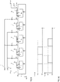
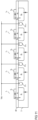
Figure 9 shows an electronic circuit that includes a plurality of electronic devices and a plurality of capacitors; -
Figure 10 shows signal diagrams of signals that may be received at clock inputs in the electronic circuit according toFigure 9 ; -
Figure 11 illustrates one example of how the first semiconductor layer in the electronic circuit according toFigure 9 may be connected to a supply potential; -
Figure 12 shows a vertical cross sectional view of a capacitor according to one example; and -
Figure 13 shows a top view of an electronic circuit of the type according toFigure 9 , wherein the capacitors are formed on top of the insulation layer. - In the following detailed description, reference is made to the accompanying drawings. The drawings form a part of the description and for the purpose of illustration show examples of how the invention may be used and implemented. It is to be understood that the features of the various embodiments described herein may be combined with each other, unless specifically noted otherwise.
-
Figure 1 shows a vertical cross sectional view andFigure 2 shows a top view of a semiconductor device according to one example. Referring toFigure 1 , the electronic device includes a first dopedregion 2 of a first doping type that is arranged in afirst semiconductor layer 3 of a second doping type complementary to the first doping type, so that a pn-junction is formed between the first dopedregion 2 and regions of thefirst semiconductor layer 3 adjoining the firstdoped region 2. This pn-junction is represented by the circuit symbol of a diode shown inFigure 1 . - Referring to
Figure 1 , the electronic device further includes aninsulation layer 4 formed on top of thefirst semiconductor layer 3, wherein theinsulation layer 4 adjoins the first dopedregion 2. More specifically, theinsulation layer 4 is formed on top of asurface 31 of thefirst semiconductor layer 3. The firstdoped region 2 extends to thesurface 31 of thefirst semiconductor layer 3, so that theinsulation layer 4 formed on top of thesurface 31 adjoins the firstdoped region 2.Figure 1 shows a vertical cross sectional view of the electronic device in a section plane that is essentially perpendicular to thesurface 31 of thefirst semiconductor layer 3 and thesurface 41 of theinsulation layer 4.Figure 2 shows a top view of thesecond semiconductor layer 5 and thesurface 41 of theinsulation layer 4. - Referring to
Figure 1 , the semiconductor device further includes asecond semiconductor layer 5 formed on top of theinsulation layer 4. More specifically, thesecond semiconductor layer 5 is formed on top of asurface 41 of theinsulation layer 4, wherein thesurface 41 of theinsulation layer 4 faces away from thefirst semiconductor layer 3. The electronic device further includes at least twoactive device regions second semiconductor layer 5. Theseactive device regions Figure 1 . More detailed examples are explained herein further below. - Referring to
Figure 1 , the electronic device further includes anelectrical connection 6 between one of the at least twoactive device regions region 2. Thiselectrical connection 6 is only schematically illustrated inFigure 1 . More detailed examples of theelectrical connection 6 are explained herein further below. - Furthermore, the
second semiconductor layer 5 is positioned on top of theinsulation layer 4 relative to a position of the firstdoped region 2 in thefirst semiconductor layer 3 such that each of the at least twoactive device regions doped region 2 and separated from the firstdoped region 2 by theinsulation layer 4. In other words, a vertical projection of each of the at least twoactive device regions first semiconductor layer 3 is located within the firstdoped region 2. This is schematically illustrated inFigure 2 in which the position of the first dopedregion 2 in thefirst semiconductor layer 3 is schematically illustrated in dashed lines. - In the example shown in
Figures 1 and 2 , thesecond semiconductor layer 5 forms an island on top of thesurface 41 of theinsulation layer 4, wherein a size of the island-likesecond semiconductor layer 5 in a horizontal plane is smaller than a size of the firstdoped region 2 in the horizontal plane, so that the vertical projection of thesecond semiconductor layer 5 onto thefirst semiconductor layer 1 is entirely within the firstdoped region 2. This, however, is only an example. According to another example (not shown) a vertical projection of thesecond semiconductor layer 5 onto thefirst semiconductor layer 3 extends beyond the firstdoped region 2. However, in each case, vertical projections of the at least twoactive device regions first semiconductor layer 3 are located within the firstdoped region 2. - According to one example, the electronic device is configured to receive a first supply potential Vo. More specifically, one of the first and second
active regions Figure 1 , a first one 52 of the at least twoactive device regions active device region 51 is that one of the at least twoactive device regions doped region 2. This, however, is only an example. The active device region connected to the firstdoped region 2 is not necessarily the active device region that receives the first supply potential Vo. According to another example (not shown) the firstactive device region 51 receives the first supply potential Vo and the secondactive region 52 is connected to the firstdoped region 21, or vice versa. - During operation of the electronic device, a voltage V5 may occur between the first
active device region 51 and the secondactive device region 52. This voltage may have a maximum magnitude, wherein the maximum magnitude may be defined by the way the electronic device is operated in an electronic circuit (not shown) that uses the electronic device, or may be defined by a voltage blocking capability of the electronic device. The "voltage blocking capability" is the maximum voltage the electronic device can withstand between the firstactive device region 51 and the secondactive device region 52. - In each case, due to connecting the first
doped region 2 to one of the first and secondactive device regions second semiconductor layer 5 and the first dopedregion 2 across theinsulation layer 4 is given by the maximum magnitude of the voltage between the first and secondactive regions - Referring to
Figure 1 , thefirst semiconductor layer 1 may be configured to receive a second electrical potential Vss that is different from the first potential Vo. According to one example, polarities of the first potential Vo and the second potential Vss and the first and second doping types of the first dopedregion 2 and adjoining regions of thefirst semiconductor layer 1 are adapted to one another such that the pn-junction between the firstdoped region 2 and the adjoining regions of thefirst semiconductor layer 3 is reverse biased when the first potential Vo is received by the one of the first and secondactive device regions first semiconductor layer 1. If, for example, the first potential Vo is positive relative to the second potential Vss, the first doping type of the firstdoped region 2 is an n-type, while the second doping type of thefirst semiconductor layer 1 is a p-type. In this way, the pn-junction between the firstdoped region 2 and the adjoining regions of thefirst semiconductor layer 1 is reverse biased when the first and second potentials Vo, Vss are applied to the electronic device. - According to one example, the
first semiconductor layer 3 comprises monocrystalline silicon (Si). Theinsulation layer 4 may include silicon oxide. Thesecond semiconductor layer 5 may include monocrystalline Si or may include Si1-xGex, wherein Ge is germanium and x is selected from between 0 and 30%. According to one example, a thickness of theinsulation layer 4 is selected from between 10 nanometers (nm) and 30 nanometers, and a thickness of thesecond semiconductor layer 5 is selected from between 5 nanometers and 15 nanometers. The "thickness" is the dimension of the respective layer in a direction perpendicular to thesurface 41 of theinsulation layer 4. -
Figures 3 and 4 show one example of the electronic device shown inFigures 1 and 2 in greater detail.Figure 3 shows a vertical cross sectional view of the electronic device andFigure 4 shows a horizontal cross sectional view in a section plane B-B that cuts through thefirst semiconductor layer 3. The "horizontal section plane" is a plane that is essentially parallel to thesurface 31 of thefirst semiconductor layer 3. - Referring to
Figure 3 , theelectrical connection 6 between the one of the at least twoactive device regions 51, 52 (the firstactive device region 51 in the example shown inFigure 3 ) and the firstdoped region 2 includes an electrically conducting via 61 that extends from thesurface 41 of theinsulation layer 4 through theinsulation layer 4 to or into the firstdoped region 2. This electrically conducting via 61 is electrically connected to the firstactive device region 51 via aconductor 63, wherein thisconductor 63 is only schematically illustrated inFigure 1 . Theconductor 63 may include any type of electrical conductor and include any type of electrically conducting material such as, for example, aluminum (Al), copper (Cu), Titanium (Ti), tungsten (W) or the like. The electrical conducting via 61 includes tungsten (W), for example. Optionally, theconductor 63 is connected to the via 61 via acontact region 62 formed on top of the via 61. According to one example, thecontact region 62 is a doped semiconductor region of the first or second doping type. According to one example, the semiconductor region forming thecontact region 62 is spaced apart from thesecond semiconductor layer 5. - Referring to
Figure 3 , the electronic device may include aninsulating region 71 that extends from thesurface 41 of theinsulation layer 4 through theinsulation layer 4 into thefirst semiconductor layer 3, wherein the insulatingregion 71 forms a collar that surrounds the conducting via 61 and asection 21 of the firstdoped region 2. According to one example, a vertical dimension of the insulatingregion 71 is such that the insulatingregion 71 extends between 100 nanometers (nm) and 500 nanometers, in particular between 200 nanometers and 400 nanometers, into thesemiconductor layer 3. The "vertical dimension" is the dimension in the vertical direction of thesemiconductor layer 3, which is a direction perpendicular to thefirst surface 31. - Optionally, the electronic device includes a further
insulating region 72. In the following, the furtherinsulating region 72 is also referred to as second insulating region, and insulatingregion 71 is also referred to as first insulating region. The secondinsulating region 72 extends from thesurface 41 of theinsulation layer 4 into thefirst semiconductor layer 3 , at least partially surrounds the firstdoped region 2, and separates those sections of the firstdoped region 2 that adjoin theinsulation layer 4 from sections of thefirst semiconductor layer 3. The secondinsulating region 72 may adjoin the firstinsulating region 71. According to one example, a vertical dimension of the secondinsulating region 72 is selected from the same range as the vertical dimension of the firstinsulating region 71, so that the secondinsulating region 72 may extend between 100 nanometers (nm) and 500 nanometers, in particular between 200 nanometers and 400 nanometers, into thesemiconductor layer 3. - According to the example illustrated in
Figure 3 , the firstinsulating region 71 and the optional secondinsulating region 72 may extend less deep into thesemiconductor layer 3 than the first doped region. According to another example (not shown), the secondinsulating region 72 extends as deep into thefirst semiconductor layer 3 as the firstdoped region 2, so that the pn-junction between the firstdoped region 2 and adjoining regions of thefirst semiconductor layer 3 is essentially parallel to theinsulation layer 4. According to yet another example (not shown), the secondinsulating region 72 extends deeper into thefirst semiconductor layer 3 than the firstdoped region 2. - According to one example, the at least two
active device regions active device regions Figure 5. Figure 5 shows a vertical cross sectional view of thesecond semiconductor layer 5 and of a section of theinsulation layer 4 adjoining thesecond semiconductor layer 5. Thefirst semiconductor layer 3 with the firstdoped region 2 and the electrical connection are not illustrated inFigure 5 . - According to one example, the first
active device region 51 is a p-type region and forms an anode of the diode, and the secondactive device region 52 is an n-type region and forms a cathode K of the diode. Furthermore, the diode may include abase region 53 of an n-type or a p-type, wherein a doping concentration of thebase region 53 is much lower than a doping concentration of each of the first and secondactive device regions active device regions base region 53 is between 1E15 cm-3 and 1E18 cm-3, for example. - It should be noted that the
base region 53 is optional. According to another example (not shown) the firstactive device region 51 forming the anode A adjoins the secondactive device region 52 forming the cathode K. - According to another example shown in
Figure 6 , the first and secondactive device regions active device regions active device regions Figure 6 , the firstactive device region 51 forms a source region S and the secondactive device region 52 forms a drain region D. Furthermore, the MOSFET includes abody region 54 arranged between thesource region 51 and thedrain region 52, and agate electrode 56. Thegate electrode 56 is arranged adjacent to thebody region 54 and is dielectrically insulated from thesecond semiconductor layer 5 by agate dielectric 55. Thegate electrode 56 is configured to control a conducting channel between thesource region 51 and drainregion 52 along thegate dielectric 55 in thebody region 54. - The MOSFET can be an n-type MOSFET or a p-type MOSFET. In an n-type MOSFET, the source and drain
regions body region 54 is p-doped. In a p-type MOSFET, thesource region 51 and thedrain region 52 are p-doped and thebody region 54 is n-doped. - Doping concentrations of the source and drain
regions body region 54 is, for example, in the range of between 1E17 cm-3 and 1E19 cm-3. - According to one example, the MOSFET shown in
Figure 6 is connected as a diode. This is explained with reference toFigure 7A - 7B and 8A - 8B in the following. -
Figures 7A and 7B show a vertical cross sectional view and an equivalent circuit diagram of an n-type MOSFET that is connected as a diode. This MOSFET may also be referred to as diode-connected MOSFET. Referring toFigure 7A , thedrain region 52 is connected to thegate electrode 56. Referring to the equivalent circuit diagram shown inFigure 7B , thedrain region 52 of the MOSFET forms the anode and thesource region 51 of the MOSFET forms the cathode of the diode. -
Figures 8A and 8B show a vertical cross sectional view and an equivalent circuit diagram of a p-type MOSFET that is connected as a diode. Referring toFigure 8A , the drain-region 52 is connected to the gate electrode 56 (which is the same as in the example shown inFigure 7A ). Different from the example shown inFigure 7B , thesource region 51 forms the anode and thedrain region 52 forms the cathode of the diode. -
Figure 9 shows one example of a charge pump circuit that includes a plurality of electronic devices 11-1N of the type explained herein before. Each of these electronic devices has a fist doped region 21-2N arranged in afirst semiconductor layer 3, wherein thefirst semiconductor layer 3 is shared by the plurality of electronic devices 11-1N. Furthermore, insulation layers 41-4N of the electronic devices 11-1N. are formed by acommon insulation layer 40 formed on top of thefirst semiconductor layer 3. Furthermore, each of the electronic devices 11-1N includes a diode integrated in a respective second semiconductor layer 51-5N. The second semiconductor layers 51-5N are formed on top of theinsulation layer 40 are spaced apart from each other. Diodes integrated in the respective second semiconductor layers 51-5N are represented by their circuit symbol in the example shown inFigure 9 . Each of these diodes may be implemented in accordance with any of the examples explained with reference toFigures 5, 6, 7A-7B, 8A-8B . - Referring to
Figure 9 , each of the electronic devices 11-1N includes an electrical connection 61-6N between an active device region in the respective second semiconductor layer 51-5N and the respective first doped region 21-2N. The active device regions are not explicitly illustrated inFigure 9 . Just for the purpose of illustration it is assumed that, in each of the electronic devices 11-1N, the active device region forming an anode of the respective diode is connected to the respective first doped region 21-2N. This, however, is only an example. According to another example, the active device region forming the cathode of the diode is connected to the respective first doped region 21-2N. It is also possible to implement the charge pump circuit in such a way that one or more of the diodes have their anode connected to the respective firstdoped region 2 and one or more of the diodes have their cathode connected to the respective firstdoped region 2. - The electronic devices 11-1N are connected in series, that is, the diodes implemented in the second semiconductor layers are connected in series between an
input node 11 and anoutput 12 in such a way that the anode of the diode in a firstelectronic device 11 of the series circuit is connected to theinput node 11, the cathode of an N-thelectronic device 1N in the series circuit is connected to the output node, and that a current may flow from theinput node 11 to theoutput node 12 via the series circuit. N is selected from between 2 and 20, for example. - The
input node 11 is configured to receive an input voltage Vin. According to one example, the input voltage Vin is referenced to the second supply potential Vss. A magnitude of the input voltage is selected from between 1V and 5V, in particular from between 1.5V and 3.3V, for example. Theoutput node 12 is configured to provide an output voltage Vout, wherein the output voltage Vout may also be referenced to the second supply potential Vss. - Furthermore, the charge pump circuit includes a plurality of taps 81-8N-1 and a plurality of capacitors 71-7N-1. Each tap 81-8N-1 is a circuit node at which the diodes of a respective pair of the electronic devices 11-1N-1 are connected, and each of the capacitors 71-7N-1 has a first node that is connected to a respective one of the taps 81-8N-1 and a second node that is connected to one of a
first clock node 12 andsecond clock node 14. More specifically, the taps 81-8N-1 includefirst taps second taps first taps second taps Capacitors first taps first clock node 13, and capacitors 72, 7N-1 that have their first node connected to one of thesecond taps second clock node 14. Optionally, the charge pump circuit further includes an output capacitor 9 that is connected to theoutput node 12 and configured to buffer the output voltage Vout. - The charge pump circuit, in a conventional way, is configured to generate the output voltage Vout based on the input voltage Vin such that the output voltage Vout is higher than the input voltage Vin. According to one example, the output voltage Vout is essentially a multiple of the input voltage Vin, wherein a multiplication factor is given by N, that is the number N of diodes 21-2N-1 and the number N-1 of capacitors 71-7N-1 plus one. For this, the
first clock input 13 may receive a first clock signal CLK1 and thesecond clock input 14 may receive a second clock signal CLK2. Each of these clock signals CLK1, CLKL2 alternates between a first signal level, such as a signal level corresponding to the voltage level of the input voltage Vin, and a second signal level, such as zero. Furthermore, the first clock signal CLK1 and the second clock signal CLK2 are complementary in such a way that they do not have the first signal level at the same time (but may have the second signal level at the same time). One way of operating the charge pump circuit is briefly explained in the following. - When the input voltage Vin is applied to the
input node 11 at least a first one 71 of the capacitors 71-7N-1 is charged during those time periods in which the first clock signal CLKlhas the second signal level, so that a voltage V71 across the first capacitor 71 essentially equals the input voltage Vin (when the voltage drop across the diode of the first electronic device is neglected). The "first capacitor 71" is the capacitor that is coupled to theinput node 11 via the diode of the firstelectronic device 1I and is connected to the to thefirst tap 81, wherein the "first tap 81" is connected to the firstelectronic device 11 at a circuit node facing away from theinput node 11. When the first clock signal CLK1 changes from the lower second signal level to the higher first signal level (such as Vin), the first capacitor 71 is discharged via the diode of the secondelectronic device 12, so that at least asecond one 72 of the capacitors 71-7N-1 is charged, wherein a voltage across thesecond capacitor 72 may reach a voltage level that is twice the voltage level of the input voltage. The "secondelectronic device 12" is the electronic device that is directly connected to the firstelectronic device 11 and the first capacitor 71, and the "second capacitor 72" is the capacitor that is connected to asecond tape 82, wherein the "second tap 82" is connected to the secondelectronic device 12 at a circuit node facing away from the firstelectronic device 11. Whenever the second clock signal CLK2 changes from the low signal level to the high signal level, the second capacitor 72 is discharged and, via the thirdelectronic device 13 charges at least a third capacitor 73, wherein a voltage across the third capacitor 73 may reach a voltage level that is essentially three times the voltage level of the input voltage, and so on. The "thirdelectronic device 13" is the electronic device that is directly connected to the secondelectronic device 12 and the second capacitor 72, and the "third capacitor 73" is the capacitor that is connected to athird tap 83, wherein the "third tap 83" is connected to the thirdelectronic device 13 at a circuit node facing away from the secondelectronic device 12. - In the charge pump circuit according to
Figure 9 , each of the taps 81-8n-1 is connected to a respective one of the first doped regions 21-2N. These taps, during operation of the charge pump circuit, have different electrical potentials. The voltage across the insulating layer 41-4N of each of the electronic devices 11-1N, however, is not higher than the voltage between the tap that is connected to the first doped region and a neighboring tap downstream the series circuit. That is, for example, the voltage across insulatinglayer 42 of the secondelectronic device 12 is given by a magnitude of the voltage betweentap 81 connected to the firstdoped region 22 of the secondelectronic device 12 and neighboringtap 82 arranged downstream in the series circuit. - Basically, the voltage between two of these taps is not higher than the input voltage Vin. Thus, even in a charge pump circuit that provides an output voltage Vout that is a multiple of the input voltage Vin, a required dielectric strength of the insulating
layer 40 is given by the input voltage Vin. A voltage blocking capability of the pn-junctions formed between the first doped regions 21-2N, however, is higher than the dielectric strength of the insulatinglayer 4. The voltage blocking capability of these pn-junctions can be adjusted by suitably adjusting the doing concentrations of the first doped regions 21-2N and a basic doping of thefirst semiconductor layer 3. - Referring to the above, the
first semiconductor layer 3 may be connected to a second electrical potential Vss, such as ground potential. According to one example illustrated inFigure 11 , thefirst semiconductor layer 3 includes a plurality of doped regions 311-31N-1 of the second doping type, wherein each of these doped regions 311-31N- 1 is arranged between a pair of first doped regions 21-2N. Each of these doped regions 311-31N-1 is connected to the second electrical potential Vss. Electrical connections between the doped regions 311-31N-1 and the second electrical potential Vss are only schematically illustrated inFigure 11 . The doped regions 311-31N-1 may be connected to the second electrical potential Vss by electrical connections of the same type as explained with reference toFigure 3 in context with connecting the firstdoped region 2 to the firstactive device region 51. - For the ease of illustration,
Figure 11 only illustrates the electronic devices 11-1N. and the doped regions 311-31N-1. The capacitors of the charge pump circuit are not illustrated inFigure 11 . - According to one example, the doped regions 311-31N-1 are part of doped rings of the second doping type, wherein each of these rings surrounds a respective one of the first doped regions 21-2N.
- According to one example, the capacitors 71-7N-1 of the charge pump circuit are formed on the same insulating
layer 40 on top of which the second semiconductor layers 51-5n are formed.Figure 12 illustrates one example of a capacitor 7 formed on top of the insulatinglayer 40. In this example, the capacitor 7 includes afirst capacitor electrode 71 formed on top of the insulatinglayer 40, acapacitor dielectric 72 formed on top of thefirst capacitor electrode 71, and asecond capacitor electrode 73 formed on top of thecapacitor dielectric 72. Thefirst capacitor electrode 71 forms a first circuit node of the capacitor 7 and thesecond capacitor electrode 73 forms a second circuit node of the capacitor 7. The first andsecond capacitor electrodes capacitor dielectric 72 may include silicon oxide, for example. -
Figure 13 schematically illustrates a top view of a charge pump circuit that includes a plurality of first electronic devices 11-1N and a plurality of capacitors 71-7N-1 formed on tops of the insulatinglayer 40. For the purpose of illustration, only the second semiconductor layers 51-5N of the electronic devices are illustrated inFigure 13 . As can be seen fromFigure 13 , these second semiconductor layers 51-5N are spaced apart from each other (as explained above) and are spaced apart from each of the capacitors 71-7N-1. Furthermore, the capacitor 71-7N-1 are spaced apart from each other. The semiconductor devices 11-1N may be connected with each other and may be connected with the respective capacitors 71-7N-1 using conventional wiring arrangements formed on top of the insulatinglayer 4. The wiring arrangement may include a further insulating layer that is formed on top of the insulatinglayer 4 and that separates conductors of the wiring arrangement from the insulating layer. The further insulating layer includes an oxide layer, a nitride layer, or the like. Such wiring arrangements are commonly known a and not illustrated in the drawings. - Some of the aspects explained above are summarized in the following by way of numbered examples.
- Example 1. An electronic device, including: a first doped region of a first doping type arranged in a first semiconductor layer of a second doping type complementary to the first doping type; an insulation layer formed on top of the first semiconductor layer and adjoining the first doped region; at least two active device regions arranged in a second semiconductor layer formed on top of the insulation layer; and an electrical connection between one of the at least two active device regions and the first doped region, wherein each of the at least two active device regions is arranged adjacent to the first doped region and separated from the first doped region by the insulation layer.
- Example 2. The electronic device of example 1, wherein the electrical connection includes: an electrically conducting via extending through the insulation layer and contacting the first doped region.
- Example 3. The electronic device of example 2, further including: a doped semiconductor region formed on top of the electrically conducting via.
- Example 4. The electronic device of example 2 or 3, further including: a trench isolation laterally surrounding a section of the first doped region that adjoins the electrically conducting via.
- Example 5. The electronic device of any one of the preceding examples, further including: a further trench isolation laterally surrounding the first doped region.
- Example 6. The electronic device of any one of examples 1 to 5, wherein the electronic device is a diode in which one of the at least two active device regions is an anode region and another one of the east two active device regions is a cathode region.
- Example 7. The electronic device of example 6, further including: a base region arranged between the anode region and the cathode region in the second semiconductor layer.
- Example 8. The electronic device of any one of examples 1 to 5, wherein the electronic device is a transistor device in which one of the at least two active device regions is a source region and another one of the at least two active device regions is a drain region, and wherein the electronic device further includes: a body region arranged in the second semiconductor layer between the source region and the drain region; and a gate electrode arranged adjacent to the body region and dielectrically insulated from the body region by a gate dielectric.
- Example 9. The electronic device of example 8, wherein the drain region is electrically connected to the gate electrode.
- Example 10. The electronic device of any one of the preceding examples, wherein the first semiconductor layer is a silicon layer, and wherein the insulation layer is a silicon oxide layer.
- Example 11. The electronic device of any one of the preceding examples, wherein the second semiconductor layer is one of a silicon layer and a silicon-germanium layer.
- Example 12. The electronic device of any one of the preceding examples, doping concentrations of the first doped region and the first semiconductor layer are adapted to one another such that a voltage blocking capability of a pn-junction formed between the first doped region and the first semiconductor layer is higher than a dielectric strength of the insulation layer.
- Example 13. An electronic circuit, including: a plurality of electronic devices each according to any one of examples 1 to 12; and a plurality of capacitors, wherein the first doped regions of the electronic devices are arranged in the same first semiconductor layer and are spaced apart from each other in the first semiconductor layer, wherein the electronic devices are connected in series, wherein each of the capacitors is connected to a respective one of a plurality of taps, wherein each tap is a circuit node between a respective pair of the electronic devices in the series circuit.
- Example 14. The electronic circuit of example 13, wherein the insulating layer of each of the electronic devices is a respective section of a common insulation layer, and wherein the capacitors are formed on top of the common insulation layer.
- Example 15. The electronic circuit of example 13 or 14, further including: a plurality of contact regions of the second doping type arranged in the first semiconductor layer and connected to a circuit node configured to receive a supply potential, wherein each of the contact regions is a arranged between a respective pair of neighboring first doped regions.
Claims (15)
- An electronic device, comprising:a first doped region (2) of a first doping type arranged in a first semiconductor layer (3) of a second doping type complementary to the first doping type;an insulation layer (4) formed on top of the first semiconductor layer (3) and adjoining the first doped region (2);at least two active device regions (51, 52) arranged in a second semiconductor layer (5) formed on top of the insulation layer (4); andan electrical connection (6) between one of the at least two active device regions (51, 52) and the first doped region (2),wherein each of the at least two active device regions (51, 52) is arranged adjacent to the first doped region (2) and separated from the first doped region (2) by the insulation layer (4).
- The electronic device of claim 1,
wherein the electrical connection (6) comprises:
an electrically conducting via (61) extending through the insulation layer (4) and contacting the first doped region (2). - The electronic device of claim 2, further comprising:
a doped semiconductor region (62) formed on top of the electrically conducting via (61). - The electronic device of claim 2 or 3, further comprising:
a trench isolation (71) laterally surrounding a section (21) of the first doped region (2) that adjoins the electrically conducting via (61). - The electronic device of any one of the preceding claims, further comprising:
a further trench isolation (72) laterally surrounding the first doped region (2). - The electronic device of any one of claims 1 to 5,
wherein the electronic device is a diode in which one of the at least two active device regions (51, 52) is an anode region (A) and another one of the east two active device regions (51, 52) is a cathode region (K). - The electronic device of claim 6, further comprising:
a base region (53) arranged between the anode region and the cathode region in the second semiconductor layer (5). - The electronic device of any one of claims 1 to 5,wherein the electronic device is a transistor device in which one of the at least two active device regions (51, 52) is a source region (S) and another one of the at least two active device regions (51, 52) is a drain region (D), andwherein the electronic device further comprises:a body region (54) arranged in the second semiconductor layer (5) between the source region (S) and the drain region (D); anda gate electrode (56) arranged adjacent to the body region (54) and dielectrically insulated from the body region (54) by a gate dielectric (55).
- The electronic device of claim 8,
wherein the drain region (D) is electrically connected to the gate electrode (56). - The electronic device of any one of the preceding claims,wherein the first semiconductor layer (3) is a silicon layer, andwherein the insulation layer (4) is a silicon oxide layer.
- The electronic device of any one of the preceding claims,
wherein the second semiconductor layer (5) is one of a silicon layer and a silicon-germanium layer. - The electronic device of any one of the preceding claims,
doping concentrations of the first doped region (2) and the first semiconductor layer (3) are adapted to one another such that a voltage blocking capability of a pn-junction formed between the first doped region (2) and the first semiconductor layer (3) is higher than a dielectric strength of the insulation layer (4). - An electronic circuit, comprising:a plurality of electronic devices (11-1N) each according to any one of claims 1 to 12; anda plurality of capacitors (71-7N-1),wherein the first doped regions (21-2N) of the electronic devices (11-1N) are arranged in the same first semiconductor layer (3) and are spaced apart from each other in the first semiconductor layer (3),wherein the electronic devices (11-1N) are connected in series,wherein each of the capacitors (71-7N-1) is connected to a respective one of a plurality of taps (81-8N-1),wherein each tap (81-8N-1) is a circuit node between a respective pair of the electronic devices (11-1N-1) in the series circuit.
- The electronic circuit of claim 13,wherein the insulating layer (41-4N) of each of the electronic devices is a respective section of a common insulation layer (40), andwherein the capacitors (71-7N-1) are formed on top of the common insulation layer (40).
- The electronic circuit of claim 13 or 14, further comprising:a plurality of contact regions (311-31N-1) of the second doping type arranged in the first semiconductor layer (3) and connected to a circuit node configured to receive a supply potential (Vss),wherein each of the contact regions (311-31N-1) is a arranged between a respective pair of neighboring first doped regions (21-2N).
Priority Applications (2)
| Application Number | Priority Date | Filing Date | Title |
|---|---|---|---|
| EP21188959.7A EP4125118A1 (en) | 2021-07-30 | 2021-07-30 | Electronic device and charge pump circuit |
| US17/873,742 US12176339B2 (en) | 2021-07-30 | 2022-07-26 | Electronic device and charge pump circuit |
Applications Claiming Priority (1)
| Application Number | Priority Date | Filing Date | Title |
|---|---|---|---|
| EP21188959.7A EP4125118A1 (en) | 2021-07-30 | 2021-07-30 | Electronic device and charge pump circuit |
Publications (1)
| Publication Number | Publication Date |
|---|---|
| EP4125118A1 true EP4125118A1 (en) | 2023-02-01 |
Family
ID=77168025
Family Applications (1)
| Application Number | Title | Priority Date | Filing Date |
|---|---|---|---|
| EP21188959.7A Pending EP4125118A1 (en) | 2021-07-30 | 2021-07-30 | Electronic device and charge pump circuit |
Country Status (2)
| Country | Link |
|---|---|
| US (1) | US12176339B2 (en) |
| EP (1) | EP4125118A1 (en) |
Citations (4)
| Publication number | Priority date | Publication date | Assignee | Title |
|---|---|---|---|---|
| US20050253197A1 (en) * | 1999-09-14 | 2005-11-17 | Sharp Kabushiki Kaisha | Semiconductor device and method of manufacturing the same |
| US20120146148A1 (en) * | 2010-12-14 | 2012-06-14 | Renesas Electronics Corporation | Semiconductor integrated circuit device |
| US20130307074A1 (en) * | 2012-05-16 | 2013-11-21 | International Business Machines Corporation | Epitaxial Semiconductor Resistor With Semiconductor Structures On Same Substrate |
| US20180337596A1 (en) * | 2017-05-19 | 2018-11-22 | Globalfoundries Inc. | Switched-capacitor charge pump with reduced diode threshold voltage and on state resistance |
Family Cites Families (2)
| Publication number | Priority date | Publication date | Assignee | Title |
|---|---|---|---|---|
| US20060125014A1 (en) * | 2004-12-14 | 2006-06-15 | Nui Chong | Diode with low junction capacitance |
| US9590120B2 (en) * | 2015-03-30 | 2017-03-07 | Tdk Corporation | MOS capacitors structures for variable capacitor arrays and methods of forming the same |
-
2021
- 2021-07-30 EP EP21188959.7A patent/EP4125118A1/en active Pending
-
2022
- 2022-07-26 US US17/873,742 patent/US12176339B2/en active Active
Patent Citations (4)
| Publication number | Priority date | Publication date | Assignee | Title |
|---|---|---|---|---|
| US20050253197A1 (en) * | 1999-09-14 | 2005-11-17 | Sharp Kabushiki Kaisha | Semiconductor device and method of manufacturing the same |
| US20120146148A1 (en) * | 2010-12-14 | 2012-06-14 | Renesas Electronics Corporation | Semiconductor integrated circuit device |
| US20130307074A1 (en) * | 2012-05-16 | 2013-11-21 | International Business Machines Corporation | Epitaxial Semiconductor Resistor With Semiconductor Structures On Same Substrate |
| US20180337596A1 (en) * | 2017-05-19 | 2018-11-22 | Globalfoundries Inc. | Switched-capacitor charge pump with reduced diode threshold voltage and on state resistance |
Also Published As
| Publication number | Publication date |
|---|---|
| US20230029591A1 (en) | 2023-02-02 |
| US12176339B2 (en) | 2024-12-24 |
Similar Documents
| Publication | Publication Date | Title |
|---|---|---|
| US20240014260A1 (en) | High voltage resistor with high voltage junction termination | |
| JP5499915B2 (en) | High voltage semiconductor device | |
| US11245002B2 (en) | Superjunction transistor arrangement and method of producing thereof | |
| US6642583B2 (en) | CMOS device with trench structure | |
| US20160149034A1 (en) | Power semiconductor device having low on-state resistance | |
| US9111849B2 (en) | High voltage resistor with biased-well | |
| US20140346590A1 (en) | Semiconductor Device, Method of Manufacturing a Semiconductor Device and Integrated Circuit | |
| US11495666B2 (en) | Semiconductor device | |
| US8076722B2 (en) | PN junction and MOS capacitor hybrid resurf transistor | |
| JP5063865B2 (en) | Semiconductor device | |
| US8134206B2 (en) | Semiconductor device | |
| US10991812B2 (en) | Transistor device with a rectifier element between a field electrode and a source electrode | |
| US12176339B2 (en) | Electronic device and charge pump circuit | |
| US10734480B2 (en) | Semiconductor device having a transistor and a conductive plate | |
| US12301099B2 (en) | RC snubber network | |
| US9142551B2 (en) | Semiconductor device having a pair of transistors that are directly coupled and capacitively coupled | |
| US20260123049A1 (en) | Semiconductor-on-insulator device including a base substrate with field control region | |
| US11682695B2 (en) | Semiconductor device having a high breakdown voltage | |
| US11682696B2 (en) | Semiconductor device having a high breakdown voltage | |
| EP4407871A1 (en) | Electronic circuit with a transistor device and a protection circuit | |
| US20170084606A1 (en) | Integrated Circuit with a Plurality of Transistors and at Least One Voltage Limiting Structure | |
| CN121751694A (en) | Semiconductor device including high voltage device |
Legal Events
| Date | Code | Title | Description |
|---|---|---|---|
| PUAI | Public reference made under article 153(3) epc to a published international application that has entered the european phase |
Free format text: ORIGINAL CODE: 0009012 |
|
| STAA | Information on the status of an ep patent application or granted ep patent |
Free format text: STATUS: THE APPLICATION HAS BEEN PUBLISHED |
|
| AK | Designated contracting states |
Kind code of ref document: A1 Designated state(s): AL AT BE BG CH CY CZ DE DK EE ES FI FR GB GR HR HU IE IS IT LI LT LU LV MC MK MT NL NO PL PT RO RS SE SI SK SM TR |
|
| STAA | Information on the status of an ep patent application or granted ep patent |
Free format text: STATUS: REQUEST FOR EXAMINATION WAS MADE |
|
| 17P | Request for examination filed |
Effective date: 20230801 |
|
| RBV | Designated contracting states (corrected) |
Designated state(s): AL AT BE BG CH CY CZ DE DK EE ES FI FR GB GR HR HU IE IS IT LI LT LU LV MC MK MT NL NO PL PT RO RS SE SI SK SM TR |