EP4124208B1 - Projection exposure apparatus for semiconductor lithography - Google Patents
Projection exposure apparatus for semiconductor lithography Download PDFInfo
- Publication number
- EP4124208B1 EP4124208B1 EP20838454.5A EP20838454A EP4124208B1 EP 4124208 B1 EP4124208 B1 EP 4124208B1 EP 20838454 A EP20838454 A EP 20838454A EP 4124208 B1 EP4124208 B1 EP 4124208B1
- Authority
- EP
- European Patent Office
- Prior art keywords
- exposure apparatus
- projection exposure
- recording device
- radiation
- optical
- Prior art date
- Legal status (The legal status is an assumption and is not a legal conclusion. Google has not performed a legal analysis and makes no representation as to the accuracy of the status listed.)
- Active
Links
Images



Classifications
-
- G—PHYSICS
- G03—PHOTOGRAPHY; CINEMATOGRAPHY; ANALOGOUS TECHNIQUES USING WAVES OTHER THAN OPTICAL WAVES; ELECTROGRAPHY; HOLOGRAPHY
- G03F—PHOTOMECHANICAL PRODUCTION OF TEXTURED OR PATTERNED SURFACES, e.g. FOR PRINTING, FOR PROCESSING OF SEMICONDUCTOR DEVICES; MATERIALS THEREFOR; ORIGINALS THEREFOR; APPARATUS SPECIALLY ADAPTED THEREFOR
- G03F7/00—Photomechanical, e.g. photolithographic, production of textured or patterned surfaces, e.g. printing surfaces; Materials therefor, e.g. comprising photoresists; Apparatus specially adapted therefor
- G03F7/70—Microphotolithographic exposure; Apparatus therefor
- G03F7/708—Construction of apparatus, e.g. environment aspects, hygiene aspects or materials
- G03F7/7085—Detection arrangement, e.g. detectors of apparatus alignment possibly mounted on wafers, exposure dose, photo-cleaning flux, stray light, thermal load
-
- G—PHYSICS
- G01—MEASURING; TESTING
- G01J—MEASUREMENT OF INTENSITY, VELOCITY, SPECTRAL CONTENT, POLARISATION, PHASE OR PULSE CHARACTERISTICS OF INFRARED, VISIBLE OR ULTRAVIOLET LIGHT; COLORIMETRY; RADIATION PYROMETRY
- G01J5/00—Radiation pyrometry, e.g. infrared or optical thermometry
- G01J5/59—Radiation pyrometry, e.g. infrared or optical thermometry using polarisation; Details thereof
-
- G—PHYSICS
- G02—OPTICS
- G02B—OPTICAL ELEMENTS, SYSTEMS OR APPARATUS
- G02B27/00—Optical systems or apparatus not provided for by any of the groups G02B1/00 - G02B26/00, G02B30/00
- G02B27/28—Optical systems or apparatus not provided for by any of the groups G02B1/00 - G02B26/00, G02B30/00 for polarising
- G02B27/281—Optical systems or apparatus not provided for by any of the groups G02B1/00 - G02B26/00, G02B30/00 for polarising used for attenuating light intensity, e.g. comprising rotatable polarising elements
-
- G—PHYSICS
- G02—OPTICS
- G02B—OPTICAL ELEMENTS, SYSTEMS OR APPARATUS
- G02B27/00—Optical systems or apparatus not provided for by any of the groups G02B1/00 - G02B26/00, G02B30/00
- G02B27/28—Optical systems or apparatus not provided for by any of the groups G02B1/00 - G02B26/00, G02B30/00 for polarising
- G02B27/288—Filters employing polarising elements, e.g. Lyot or Solc filters
-
- G—PHYSICS
- G02—OPTICS
- G02B—OPTICAL ELEMENTS, SYSTEMS OR APPARATUS
- G02B5/00—Optical elements other than lenses
- G02B5/08—Mirrors
- G02B5/0891—Ultraviolet [UV] mirrors
-
- G—PHYSICS
- G02—OPTICS
- G02B—OPTICAL ELEMENTS, SYSTEMS OR APPARATUS
- G02B5/00—Optical elements other than lenses
- G02B5/08—Mirrors
- G02B5/09—Multifaceted or polygonal mirrors, e.g. polygonal scanning mirrors; Fresnel mirrors
-
- G—PHYSICS
- G02—OPTICS
- G02B—OPTICAL ELEMENTS, SYSTEMS OR APPARATUS
- G02B5/00—Optical elements other than lenses
- G02B5/30—Polarising elements
- G02B5/3025—Polarisers, i.e. arrangements capable of producing a definite output polarisation state from an unpolarised input state
- G02B5/3066—Polarisers, i.e. arrangements capable of producing a definite output polarisation state from an unpolarised input state involving the reflection of light at a particular angle of incidence, e.g. Brewster's angle
-
- G—PHYSICS
- G02—OPTICS
- G02B—OPTICAL ELEMENTS, SYSTEMS OR APPARATUS
- G02B7/00—Mountings, adjusting means, or light-tight connections, for optical elements
- G02B7/18—Mountings, adjusting means, or light-tight connections, for optical elements for prisms; for mirrors
- G02B7/181—Mountings, adjusting means, or light-tight connections, for optical elements for prisms; for mirrors with means for compensating for changes in temperature or for controlling the temperature; thermal stabilisation
- G02B7/1815—Mountings, adjusting means, or light-tight connections, for optical elements for prisms; for mirrors with means for compensating for changes in temperature or for controlling the temperature; thermal stabilisation with cooling or heating systems
-
- G—PHYSICS
- G03—PHOTOGRAPHY; CINEMATOGRAPHY; ANALOGOUS TECHNIQUES USING WAVES OTHER THAN OPTICAL WAVES; ELECTROGRAPHY; HOLOGRAPHY
- G03F—PHOTOMECHANICAL PRODUCTION OF TEXTURED OR PATTERNED SURFACES, e.g. FOR PRINTING, FOR PROCESSING OF SEMICONDUCTOR DEVICES; MATERIALS THEREFOR; ORIGINALS THEREFOR; APPARATUS SPECIALLY ADAPTED THEREFOR
- G03F7/00—Photomechanical, e.g. photolithographic, production of textured or patterned surfaces, e.g. printing surfaces; Materials therefor, e.g. comprising photoresists; Apparatus specially adapted therefor
- G03F7/70—Microphotolithographic exposure; Apparatus therefor
- G03F7/708—Construction of apparatus, e.g. environment aspects, hygiene aspects or materials
- G03F7/70858—Environment aspects, e.g. pressure of beam-path gas, temperature
- G03F7/70883—Environment aspects, e.g. pressure of beam-path gas, temperature of optical system
- G03F7/70891—Temperature
Definitions
- the invention relates to a projection exposure apparatus for semiconductor lithography.
- Such apparatuses are used for producing extremely fine structures, in particular on semiconductor components or other microstructured component parts.
- the operating principle of said apparatuses is based on the production of very fine structures down to the nanometre range by way of generally reducing imaging of structures on a mask, a so-called reticle, on an element to be structured, a so-called wafer, that is provided with photosensitive material.
- the minimum dimensions of the structures produced are directly dependent on the wavelength of the light used.
- light sources having an emission wavelength in the range of a few nanometres, for example between 1 nm and 120 nm, in particular in the region of 13.5 nm, have increasingly been used.
- the wavelength range around 13.5 nm is also referred to as the EUV range.
- the microstructured component parts are also produced using commercially established DUV systems, which have a wavelength of between 100 nm and 400 nm, in particular 193 nm.
- DUV systems which have a wavelength of between 100 nm and 400 nm, in particular 193 nm.
- the demands in respect of the optical correction of the DUV systems with a wavelength of 193 nm there is an increase in the throughput of each new generation of projection exposure apparatuses, independently of the wavelength, so as to increase the profitability; this typically leads to a greater thermal load and hence to more imaging aberrations caused by the heat.
- optical assemblies such as manipulators, for example, which alter the position and alignment of the optical elements or else influence the imaging properties of the optical elements, in particular mirrors, by deforming the optical effective surfaces.
- an optical effective surface should be understood to mean that part of a surface of an optical element which is impinged on by used light for the imaging of structures.
- the optical elements of the optical assemblies which are embodied as mirrors can be temperature-regulated by means of direct water cooling.
- the mirrors comprise cutouts which are embodied as cooling channels and which are arranged in one or more planes at different distances from the optical effective surface and through which temperature-regulated water flows. An accurate measurement of the surface temperature is advantageous for both approaches.
- US patent publication US 2013/176544 A1 discloses an arrangement for mirror temperature measurement in a microlithographic projection exposure system.
- the temperature is measured through an access channel from the rear side of the mirror.
- US2010/014060 A1 describes a temperature measurement on an optical element using a special coating or a Bragg reflector.
- German Patent Application DE 10 2018 212 400 A1 discloses the temperature monitoring of a mirror by means of infrared sensors from its rear side.
- the patent applications US20040051984 A1 and US20160091798 A1 disclose a projection exposure apparatus comprising an infrared camera, which detects the temperature of the surface of a mirror. That has the disadvantage, however, that the infrared camera detects not only the radiation emitted from the surface of the mirror but also the radiation of the thermal radiation reflected from the surroundings at the mirror surface and, as a result, a differential between the temperature of the mirror surface and the surroundings cannot be determined with a sufficient accuracy.
- a projection exposure apparatus for semiconductor lithography comprises at least one optical element and at least one temperature recording device for detecting a temperature on an optical effective surface of the optical element by means of the thermal electromagnetic radiation emitted or reflected from the optical effective surface of the optical element.
- the device comprises a polarisation filter for filtering the electromagnetic radiation.
- the filter can be arranged between the temperature recording device and the optical element.
- the filter is embodied as a polarisation filter.
- a polarisation filter This makes use of the fact that a predominant proportion of the disturbing radiation does not originally originate from the surface of the optical element, but rather emanates from other constituent parts of the projection exposure apparatus and has only been reflected from the surface of the optical element in the direction of the temperature recording device.
- a partial or complete polarisation occurs, however, when electromagnetic radiation is reflected at interfaces, that is to say that portions of radiation that are polarised perpendicularly to the plane of incidence of the radiation are predominantly reflected by the surface of the optical element.
- the interface thus acts in the manner of a polariser in a polariser/analyser arrangement.
- the portions of radiation mentioned can then be filtered out by the polarisation filter arranged upstream of the temperature recording device, said polarisation filter acting as an analyser in this case.
- the radiation emitted by the surroundings that is to say for example the housing surrounding the optical element, and reflected by the optical effective surface can be partly or completely suppressed, such that primarily the unpolarised radiation emitted by the optical effective surface itself or considerable portions of this radiation impinge(s) on the temperature recording device and can be detected by the latter.
- the temperature recording device is arranged in such a way that the radiation reflected at the surface and incident on the temperature recording device is reflected at an angle close to the Brewster angle.
- the Brewster angle is the angle at which the reflected light, when radiation is incident on an interface between two media, is polarised maximally perpendicularly to the plane of incidence of the radiation.
- the Brewster angle is dependent on the refractive indices of the two media and the frequency of the electromagnetic radiation and is 55.59° for the interface between air and SiO2, for example.
- the polarisation filter can be embodied as a rotating polarisation filter.
- a known frequency can be impressed on the intensity of the reflected, polarised thermal radiation, said intensity being detected by the temperature recording device.
- the signal portion attributed to reflected (and unwanted) radiation can easily be identified by the temperature recording device and is taken into account in the determination of the surface temperature of the optical element.
- the device can comprise a lock-in amplifier.
- a lock-in amplifier amplifies a weak electrical signal which is modulated with a known frequency and phase.
- the radiation used for imaging a structure onto a wafer is usually clocked.
- an optical element embodied as a mirror can be irradiated with a clocking of 0.2 second radiation on and 0.5 second radiation off. In the case described, this can have the effect that the bulk material of the mirror reaches a temperature of approximately 60° Celsius, but the topmost layers of the mirror reach a surface temperature of between e.g. approximately 60° Celsius and 120° Celsius which changes cyclically over time.
- This cyclically hot topmost layer is very thin and its proportion of the total thermal radiation is likewise small as a result; it may correspond in particular only to 0.1% of the total thermal radiation of the mirror.
- this clocked signature of the radiation can be amplified, detected and determined with the aid of the lock-in technique.
- the lock-in technique can also make it possible to dispense with the use of a filter.
- Each of these variants by itself or else in combination with one or more other variants can also be realised without the use of a filter.
- At least one element of the projection exposure apparatus whose radiation impinges on the temperature recording device as a result of reflection at the optical element can be configured to be temperature-regulated. What is achieved thereby is that radiation which reaches the temperature recording device and which does not originate directly from the surface - of interest for the measurement - of the optical element is emitted at least by an element whose temperature and thus whose thermal radiation can be controlled.
- the error contribution of the thermal radiation reflected on the surface of the optical element can be managed better than has been possible hitherto according to the prior art.
- the surface of the optical element can comprise a coating having an emissivity for the wavelength range detected by the temperature recording device of 0.1, preferably greater than 0.4, and particularly preferably of greater than 0.95.
- the surfaces of the optical element usually have coatings for reflecting electromagnetic radiation having a wavelength of between 1 nm and 400 nm.
- An additional layer which does not reduce the reflectivity in the range of 1 ⁇ m to 400 ⁇ m and can increase the emissivity of the surface for a wavelength of e.g. 1 ⁇ m to 15 ⁇ m to the values described further above, can therefore be formed on the surface. It goes without saying that it is also conceivable to increase the emissivity for wavelengths outside the range mentioned.
- At least one element of the projection exposure apparatus whose radiation impinges on the temperature recording device as a result of reflection at the optical element can be embodied in such a way that the emissivity for the wavelength range detected by the temperature recording device is greater than 0.4, preferably greater than 0.7, and particularly preferably greater than 0.95.
- the element can likewise be coated, wherein a functional layer, as in the case of the optical element for semiconductor lithography, does not have to be taken into account here. In this case, the element acts like a beam trap for thermal radiation emanating from the surroundings since the high emissivity mentioned is also accompanied by a high absorbance.
- the temperature recording device can comprise an IR camera.
- the temperature recording device can be designed to detect a partial region of the surface of the optical element.
- the radiation detected by the IR camera as a result of reflection at the optical element which radiation represents disturbing parasitic radiation for the detection of the surface temperature of the optical effective surface, can be reduced to a minimum.
- the cameras can detect different partial regions of the optical element.
- the temperature recording device can be configured to detect in a scanning fashion the radiation emitted or reflected by the optical element.
- the temperature recording device can be movable in such a way that the radiation emitted or reflected by the optical element is detected in a scanning fashion.
- an optical unit of the temperature recording device can be moved in such a way that the radiation emitted or reflected by the optical element is detected in a scanning fashion.
- the scanning detection of the radiation has the advantage that infrared cameras having a narrow field of view can be used.
- the scanning movement can also be embodied in such a way that the angle of the detected radiation is always close to the Brewster angle even in the case of concave or convex surfaces of the optical element. In this context, close to the Brewster angle is taken to mean that the angle is reached with a deviation of e.g. a maximum of 10°.
- Figure 1 illustrates an exemplary projection exposure apparatus 1 in which the invention can be used.
- the projection exposure apparatus 1 serves for the exposure of structures on a substrate which is coated with photosensitive materials, and which generally consists predominantly of silicon and is referred to as a wafer 2, for the production of semiconductor components, such as computer chips.
- the projection exposure apparatus 1 substantially comprises an illumination device 3 for illuminating an object field 8 in an object plane 9, a reticle holder 6 for receiving and exactly positioning a mask provided with a structure and arranged in the object plane 9, said mask being a so-called reticle 7, which is used to determine the structures on the wafer 2, a wafer holder 10 for mounting, moving and exactly positioning precisely said wafer 2, and an imaging device, namely a projection optical unit 13, having a plurality of optical elements 14, which are held by way of mounts 15 in a lens housing 16 of the projection optical unit 13.
- the basic functional principle in this case provides for the structures introduced into the reticle 7 to be imaged on the wafer 2, the imaging generally reducing the scale.
- a light source 4 of the illumination device 3 provides a projection beam 17 in the form of electromagnetic radiation, said projection beam being required for the imaging of the reticle 7 arranged in the object plane 9 onto the wafer 2 arranged in the region of an image field 11 in an image plane 12, said electromagnetic radiation being in a wavelength range of between 100 nm and 300 nm, in particular.
- a laser, a plasma source or the like can be used as source 4 for this radiation, also referred to hereinafter as used light.
- the radiation is shaped by means of optical elements 18 in an illumination optical unit 5 of the illumination device 3 in such a way that the projection beam 17, when incident on the reticle 7 arranged in the object plane 9, illuminates the object field 8 with the desired properties with regard to diameter, polarisation, shape of the wavefront and the like.
- An image of the reticle 7 is generated by way of the projection beam 17 and, after having been correspondingly reduced by the projection optical unit 13, is transferred to the wafer 2 arranged in the image plane 12, as has already been explained above.
- the reticle 7 and the wafer 2 can be moved synchronously, so that regions of the reticle 7 are imaged onto corresponding regions of the wafer 2 virtually continuously during a so-called scanning process.
- the projection optical unit 13 has a multiplicity of individual refractive, diffractive and/or reflective optical elements 14, such as for example lens elements, mirrors, prisms, terminating plates and the like, wherein said optical elements 14 can be actuated for example by means of one or a plurality of actuator arrangements, not illustrated separately in the figure.
- Figure 2 shows by way of example the basic construction of a microlithographic EUV projection exposure apparatus 101 in which the invention can likewise find application.
- the construction of the projection exposure apparatus 101 and the principle of the imaging of a structure on a reticle 107 arranged in the object plane 109 onto a wafer 102 arranged in the image plane 112 are comparable to the construction and procedure described in Figure 1 .
- Identical component parts are designated by a reference sign increased by 100 relative to Figure 1 , i.e. the reference signs in Figure 2 begin with 101.
- optical elements 114, 118 embodied as mirrors can be used for imaging and/or for illumination on account of the short wavelength of the EUV radiation 117 used as used light in the range of 1 nm to 120 nm, in particular of 13.5 nm.
- the illumination device 103 of the projection exposure apparatus 101 comprises, besides a light source 104, an illumination optical unit 105 for the illumination of the object field 108 in an object plane 109.
- the EUV radiation 117 in the form of optical used radiation generated by the light source 104 is aligned by means of a collector, which is integrated in the light source 104, in such a way that it passes through an intermediate focus in the region of an intermediate focal plane 119 before it is incident on a field facet mirror 120. Downstream of the field facet mirror 120, the EUV radiation 117 is reflected by a pupil facet mirror 121.
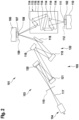
- FIG 3 shows a detail view of a projection exposure apparatus 1, 101 as described in Figure 1 or Figure 2 , in which an optical element embodied as a mirror 20 and arranged in a housing 23 is illustrated.
- the housing 23 comprises a cutout 24 closed off by a window 25, thereby avoiding gas exchange with the surroundings through the cutout 24.
- a temperature recording device embodied as an infrared camera 26 in the example shown detects, through the window 25, partly or completely the optical effective surface 22 irradiated with used light 17, 117 as that part of the surface of the mirror 20 which is under consideration in this case.
- the window 25 is transmissive to the thermal radiation 33, 34 which is detected by the infrared camera 26 and which is relevant to the temperature determination.
- the temperature recording device can also be situated elsewhere, in particular also within the housing.
- a window would not be necessary in this case.
- the mechanical links of the mirror 20 and of the infrared camera 26 to the housing 23 are not illustrated for reasons of clarity.
- the illustration likewise does not show one or a plurality of optional temperature sensors in the mirror material, which can be used for calibration purposes, in particular.
- the optical effective surface 22 of the mirror is heated as a result of absorption of used light 17, 117, wherein the temperature on the optical effective surface 22 is not constant on account of the non-constant distribution of the used light 17, 117 on the optical effective surface 22 and different heat flows in the mirror 20. Actuators can compensate for possibly unwanted rigid body movements of the mirror.
- the mirror 20 can be temperature-regulated by a temperature-regulating device (not illustrated) and/or can be deformed by actuators (not illustrated), which can be arranged at the rear side of the mirror 20, for example, in such a way that the deformations formed as a result of the heating of the mirror 20 are compensated for.
- a temperature-regulating device not illustrated
- actuators not illustrated
- the surface temperature of the optical effective surface 22 is determined by the infrared camera 26 comprising a filter 30 and a controller 31.
- the controller 31 is connected to the infrared camera 26 via a line 35, wherein in the case where the mirror 20 is cooled and/or deformed, the temperature-regulating device and/or the actuators are/is likewise connected to the controller 31.
- the infrared camera 26 sees only the thermal radiation 34 emitted by the mirror 20 and the thermal radiation 33 emitted by a part 23.1 of the housing 23 and reflected by the mirror 20.
- the controller 31 comprises a lock-in amplifier 32, which can enable an improved determination of the thermal radiation 34 emitted by the optical effective surface 22 against the background of the thermal radiation 33 emitted by the housing part 23.1.
- the thermal radiation 34 of the irradiated surface 22 comprises a constant portion and a cyclic portion caused by the cyclic exposure of the mirror 20 during the operation of the projection exposure apparatus.
- the optical effective surface 22 is irradiated for example with a clocking of 0.2 seconds "light on” and 0.5 seconds "light off”.
- the bulk material of the mirror 20 would have a temperature of approximately 60° Celsius but the topmost layers of the mirror 20 would have a surface temperature of between e.g. approximately 60° Celsius and e.g. approximately 120° Celsius that changes cyclically over time.
- This topmost layer is small and its proportion of the total thermal radiation is likewise small as a result; it may correspond in particular only to 0.1% of the total thermal radiation of the mirror surface.
- this clocked signature of the thermal radiation 34 can be amplified, detected and determined with the aid of the lock-in technique.
- the controller 31 is connected by a line 36 to the illumination or the illumination controller (neither being illustrated) of the projection exposure apparatus, via which the clocking of the used light 17, 117 is communicated to the controller 31.
- the ratio of the thermal radiation 34 emitted by the housing part 23.1 and the thermal radiation 34 emitted by the optical effective surface 22 can also be increased by means of the setting of the emissivities of the housing part 23.1 imaged onto the infrared camera 26 and of the optical effective surface 22 for the wavelength range detected by the infrared camera 26.
- the emissivity at least for the imaged part of the housing 23 is reduced and that of the irradiated surface 22 is increased, which will be described below with reference to Figures 4 , 5 and 6 .
- FIG 4 shows a detail view of the mirror 20 and of the housing 23.
- the thermal radiation 33.1 emitted by the housing part 23.1 is initially not polarised.
- said thermal radiation is polarised primarily perpendicularly for angles of incidence of greater than 0°.
- the thermal radiation 33.2 arriving at the infrared camera 26, said thermal radiation being emitted by the partial housing 23.1 and reflected at the mirror 20, is thus oriented primarily perpendicular to the plane of incidence of the radiation 33.1 on the mirror 20. This effect is particularly pronounced in particular if the thermal radiation 33.1 is reflected at an angle of reflection close to the Brewster angle.
- close should be understood to mean a deviation of the angle of incidence from the Brewster angle of less than 10°.
- the filter 30 arranged between the mirror 20 and the infrared camera 26 blocks the perpendicular polarisation direction, however, such that only the parallel polarisation direction, that is to say the portions of the thermal radiation 33.2 which are oriented parallel to the plane of incidence, impinge on the infrared camera 26.
- the ratio of reflected thermal radiation 33.2 of the housing part 23.1 and the thermal radiation 34 of the mirror 20 is decreased further and the determination of the temperature of the optical effective surface 22 is additionally simplified as a result.
- the filter 30 can also be embodied as a rotating polarisation filter, whereby a known frequency is impressed on the intensity of the reflected, polarised thermal radiation, said intensity being detected by the IR camera 26. In this way, the signal portion attributed to reflected (and unwanted) radiation is easily identified by the IR camera 26 and taken into account in the determination of the surface temperature of the optical element.
- a combination of the filter 30 and the lock-in technique is also possible.
- the infrared camera 26 itself or only an optical unit 37 can be mounted in a movable fashion, such that the optical effective surface 22 can be scanned.
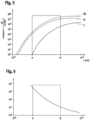
- Figure 5 shows a diagram in which the spectral radiance in W/(m 2 mSr), referred to hereinafter just as radiance, is plotted against the wavelength in a double logarithmic plot.
- the wavelength is plotted on the abscissa and the radiance is plotted on the ordinate.
- the range bounded by the points A and B on the abscissa represents the wavelength range in which the infrared camera detects thermal radiation, which range is between 2 ⁇ m and 5 ⁇ m in the example shown.
- Curve I shows the radiance of the housing part 23.1 temperature-regulated to -20° Celsius, said housing part being illustrated in Figures 3 and 4 .
- Figure 6 shows a diagram in which the ratio of curves I and II illustrated in Figure 5 is plotted likewise in a double logarithmic plot.
- the wavelength is again plotted on the abscissa and the ratio of the radiances is plotted on the ordinate.
- the ratio is between 12 and 1500.
- the ratio of the radiances of optical effective surface 22 and housing part 23.1 is still more than 450, which is sufficient for determining the surface temperature of the irradiated surface with an accuracy of +/- 1° K.
Landscapes
- Physics & Mathematics (AREA)
- General Physics & Mathematics (AREA)
- Optics & Photonics (AREA)
- Health & Medical Sciences (AREA)
- Environmental & Geological Engineering (AREA)
- Engineering & Computer Science (AREA)
- Epidemiology (AREA)
- Public Health (AREA)
- Life Sciences & Earth Sciences (AREA)
- Atmospheric Sciences (AREA)
- Toxicology (AREA)
- Spectroscopy & Molecular Physics (AREA)
- Exposure Of Semiconductors, Excluding Electron Or Ion Beam Exposure (AREA)
- Exposure And Positioning Against Photoresist Photosensitive Materials (AREA)
- Radiation Pyrometers (AREA)
Description
- The invention relates to a projection exposure apparatus for semiconductor lithography.
- Such apparatuses are used for producing extremely fine structures, in particular on semiconductor components or other microstructured component parts. The operating principle of said apparatuses is based on the production of very fine structures down to the nanometre range by way of generally reducing imaging of structures on a mask, a so-called reticle, on an element to be structured, a so-called wafer, that is provided with photosensitive material. The minimum dimensions of the structures produced are directly dependent on the wavelength of the light used. Recently, light sources having an emission wavelength in the range of a few nanometres, for example between 1 nm and 120 nm, in particular in the region of 13.5 nm, have increasingly been used. The wavelength range around 13.5 nm is also referred to as the EUV range. Apart from EUV systems, the microstructured component parts are also produced using commercially established DUV systems, which have a wavelength of between 100 nm and 400 nm, in particular 193 nm. As a result of introducing the EUV range, and hence the possibility of being able to produce even smaller structures, there has also been a further increase in the demands in respect of the optical correction of the DUV systems with a wavelength of 193 nm. Additionally, there is an increase in the throughput of each new generation of projection exposure apparatuses, independently of the wavelength, so as to increase the profitability; this typically leads to a greater thermal load and hence to more imaging aberrations caused by the heat. To correct the imaging aberrations, use can be made of optical assemblies, such as manipulators, for example, which alter the position and alignment of the optical elements or else influence the imaging properties of the optical elements, in particular mirrors, by deforming the optical effective surfaces. In this case, an optical effective surface should be understood to mean that part of a surface of an optical element which is impinged on by used light for the imaging of structures. Alternatively, the optical elements of the optical assemblies which are embodied as mirrors can be temperature-regulated by means of direct water cooling. For this purpose, the mirrors comprise cutouts which are embodied as cooling channels and which are arranged in one or more planes at different distances from the optical effective surface and through which temperature-regulated water flows. An accurate measurement of the surface temperature is advantageous for both approaches.
- Exemplary solutions for temperature measurement are disclosed in several publications.
- For example, US patent publication
US 2013/176544 A1 discloses an arrangement for mirror temperature measurement in a microlithographic projection exposure system. In this case, the temperature is measured through an access channel from the rear side of the mirror. -
US2010/014060 A1 describes a temperature measurement on an optical element using a special coating or a Bragg reflector. - International Patent Application
WO 2014/001071 A1 discloses the monitoring of a collector mirror of a source using infrared sensors. - German
Patent Application DE 10 2018 212 400 A1 discloses the temperature monitoring of a mirror by means of infrared sensors from its rear side. The patent applicationsUS20040051984 A1 andUS20160091798 A1 disclose a projection exposure apparatus comprising an infrared camera, which detects the temperature of the surface of a mirror. That has the disadvantage, however, that the infrared camera detects not only the radiation emitted from the surface of the mirror but also the radiation of the thermal radiation reflected from the surroundings at the mirror surface and, as a result, a differential between the temperature of the mirror surface and the surroundings cannot be determined with a sufficient accuracy. - It is an object of the present invention to provide a device which eliminates the above-described disadvantages of the prior art.
- This object is achieved by a device having features of the independent claim. The dependent claims relate to advantageous developments and variants of the invention. A projection exposure apparatus for semiconductor lithography according to the invention comprises at least one optical element and at least one temperature recording device for detecting a temperature on an optical effective surface of the optical element by means of the thermal electromagnetic radiation emitted or reflected from the optical effective surface of the optical element. According to the invention the device comprises a polarisation filter for filtering the electromagnetic radiation.
- The filter can be arranged between the temperature recording device and the optical element. By virtue of the fact that the radiation used for detecting the temperature is filtered before it reaches the temperature recording device, disturbing radiation that cannot be used for determining the temperature of the surface or would corrupt the measurement can be masked out, with the result that the accuracy of the temperature measurement is improved.
- According to the invention, the filter is embodied as a polarisation filter. This makes use of the fact that a predominant proportion of the disturbing radiation does not originally originate from the surface of the optical element, but rather emanates from other constituent parts of the projection exposure apparatus and has only been reflected from the surface of the optical element in the direction of the temperature recording device. A partial or complete polarisation occurs, however, when electromagnetic radiation is reflected at interfaces, that is to say that portions of radiation that are polarised perpendicularly to the plane of incidence of the radiation are predominantly reflected by the surface of the optical element. The interface thus acts in the manner of a polariser in a polariser/analyser arrangement. The portions of radiation mentioned can then be filtered out by the polarisation filter arranged upstream of the temperature recording device, said polarisation filter acting as an analyser in this case. As a result, the radiation emitted by the surroundings, that is to say for example the housing surrounding the optical element, and reflected by the optical effective surface can be partly or completely suppressed, such that primarily the unpolarised radiation emitted by the optical effective surface itself or considerable portions of this radiation impinge(s) on the temperature recording device and can be detected by the latter.
- In this case, it may be advantageous if the temperature recording device is arranged in such a way that the radiation reflected at the surface and incident on the temperature recording device is reflected at an angle close to the Brewster angle. The Brewster angle is the angle at which the reflected light, when radiation is incident on an interface between two media, is polarised maximally perpendicularly to the plane of incidence of the radiation. The Brewster angle is dependent on the refractive indices of the two media and the frequency of the electromagnetic radiation and is 55.59° for the interface between air and SiO2, for example.
- Furthermore, the polarisation filter can be embodied as a rotating polarisation filter. As a result, a known frequency can be impressed on the intensity of the reflected, polarised thermal radiation, said intensity being detected by the temperature recording device. In this way, the signal portion attributed to reflected (and unwanted) radiation can easily be identified by the temperature recording device and is taken into account in the determination of the surface temperature of the optical element.
- To improve the measurement accuracy further, the device can comprise a lock-in amplifier. A lock-in amplifier amplifies a weak electrical signal which is modulated with a known frequency and phase. In the case of a projection exposure apparatus, the radiation used for imaging a structure onto a wafer is usually clocked. In this regard, by way of example, an optical element embodied as a mirror can be irradiated with a clocking of 0.2 second radiation on and 0.5 second radiation off. In the case described, this can have the effect that the bulk material of the mirror reaches a temperature of approximately 60° Celsius, but the topmost layers of the mirror reach a surface temperature of between e.g. approximately 60° Celsius and 120° Celsius which changes cyclically over time. This cyclically hot topmost layer is very thin and its proportion of the total thermal radiation is likewise small as a result; it may correspond in particular only to 0.1% of the total thermal radiation of the mirror. However, exactly this clocked signature of the radiation can be amplified, detected and determined with the aid of the lock-in technique.
- The lock-in technique can also make it possible to dispense with the use of a filter. The same applies to the variants described below. Each of these variants by itself or else in combination with one or more other variants can also be realised without the use of a filter.
- Furthermore, at least one element of the projection exposure apparatus whose radiation impinges on the temperature recording device as a result of reflection at the optical element can be configured to be temperature-regulated. What is achieved thereby is that radiation which reaches the temperature recording device and which does not originate directly from the surface - of interest for the measurement - of the optical element is emitted at least by an element whose temperature and thus whose thermal radiation can be controlled. By means of the measure according to the invention, the error contribution of the thermal radiation reflected on the surface of the optical element can be managed better than has been possible hitherto according to the prior art.
- Additionally or alternatively, the surface of the optical element can comprise a coating having an emissivity for the wavelength range detected by the temperature recording device of 0.1, preferably greater than 0.4, and particularly preferably of greater than 0.95. The surfaces of the optical element usually have coatings for reflecting electromagnetic radiation having a wavelength of between 1 nm and 400 nm. An additional layer, which does not reduce the reflectivity in the range of 1 µm to 400 µm and can increase the emissivity of the surface for a wavelength of e.g. 1 µm to 15 µm to the values described further above, can therefore be formed on the surface. It goes without saying that it is also conceivable to increase the emissivity for wavelengths outside the range mentioned.
- In one advantageous variant of the invention, at least one element of the projection exposure apparatus whose radiation impinges on the temperature recording device as a result of reflection at the optical element can be embodied in such a way that the emissivity for the wavelength range detected by the temperature recording device is greater than 0.4, preferably greater than 0.7, and particularly preferably greater than 0.95. The element can likewise be coated, wherein a functional layer, as in the case of the optical element for semiconductor lithography, does not have to be taken into account here. In this case, the element acts like a beam trap for thermal radiation emanating from the surroundings since the high emissivity mentioned is also accompanied by a high absorbance.
- Furthermore, the temperature recording device can comprise an IR camera.
- In particular, the temperature recording device can be designed to detect a partial region of the surface of the optical element. By limiting the field of view of the camera, the radiation detected by the IR camera as a result of reflection at the optical element, which radiation represents disturbing parasitic radiation for the detection of the surface temperature of the optical effective surface, can be reduced to a minimum. In the case of a plurality of cameras, the cameras can detect different partial regions of the optical element.
- Furthermore, the temperature recording device can be configured to detect in a scanning fashion the radiation emitted or reflected by the optical element.
- In particular, the temperature recording device can be movable in such a way that the radiation emitted or reflected by the optical element is detected in a scanning fashion.
- It may also be advantageous if an optical unit of the temperature recording device can be moved in such a way that the radiation emitted or reflected by the optical element is detected in a scanning fashion. The scanning detection of the radiation has the advantage that infrared cameras having a narrow field of view can be used. The scanning movement can also be embodied in such a way that the angle of the detected radiation is always close to the Brewster angle even in the case of concave or convex surfaces of the optical element. In this context, close to the Brewster angle is taken to mean that the angle is reached with a deviation of e.g. a maximum of 10°.
- Exemplary embodiments and variants of the invention are explained in more detail below with reference to the drawing. In the figures:
- Figure 1
- shows the basic construction of a DUV projection exposure apparatus in which the invention can be implemented,
- Figure 2
- shows the basic construction of an EUV projection exposure apparatus in which the invention can be implemented,
- Figure 3
- shows a detail view of the invention,
- Figure 4
- shows a further detail view of the invention,
- Figure 5
- shows a diagram illustrating radiances versus wavelengths, and
- Figure 6
- shows a diagram illustrating the ratio of two radiances versus wavelength.
-
Figure 1 illustrates an exemplaryprojection exposure apparatus 1 in which the invention can be used. Theprojection exposure apparatus 1 serves for the exposure of structures on a substrate which is coated with photosensitive materials, and which generally consists predominantly of silicon and is referred to as awafer 2, for the production of semiconductor components, such as computer chips. - In this case, the
projection exposure apparatus 1 substantially comprises anillumination device 3 for illuminating anobject field 8 in anobject plane 9, areticle holder 6 for receiving and exactly positioning a mask provided with a structure and arranged in theobject plane 9, said mask being a so-calledreticle 7, which is used to determine the structures on thewafer 2, awafer holder 10 for mounting, moving and exactly positioning precisely saidwafer 2, and an imaging device, namely a projectionoptical unit 13, having a plurality ofoptical elements 14, which are held by way ofmounts 15 in alens housing 16 of the projectionoptical unit 13. - The basic functional principle in this case provides for the structures introduced into the
reticle 7 to be imaged on thewafer 2, the imaging generally reducing the scale. - A light source 4 of the
illumination device 3 provides aprojection beam 17 in the form of electromagnetic radiation, said projection beam being required for the imaging of thereticle 7 arranged in theobject plane 9 onto thewafer 2 arranged in the region of animage field 11 in animage plane 12, said electromagnetic radiation being in a wavelength range of between 100 nm and 300 nm, in particular. A laser, a plasma source or the like can be used as source 4 for this radiation, also referred to hereinafter as used light. The radiation is shaped by means ofoptical elements 18 in an illumination optical unit 5 of theillumination device 3 in such a way that theprojection beam 17, when incident on thereticle 7 arranged in theobject plane 9, illuminates theobject field 8 with the desired properties with regard to diameter, polarisation, shape of the wavefront and the like. - An image of the
reticle 7 is generated by way of theprojection beam 17 and, after having been correspondingly reduced by the projectionoptical unit 13, is transferred to thewafer 2 arranged in theimage plane 12, as has already been explained above. In this case, thereticle 7 and thewafer 2 can be moved synchronously, so that regions of thereticle 7 are imaged onto corresponding regions of thewafer 2 virtually continuously during a so-called scanning process. The projectionoptical unit 13 has a multiplicity of individual refractive, diffractive and/or reflectiveoptical elements 14, such as for example lens elements, mirrors, prisms, terminating plates and the like, wherein saidoptical elements 14 can be actuated for example by means of one or a plurality of actuator arrangements, not illustrated separately in the figure. -
Figure 2 shows by way of example the basic construction of a microlithographic EUVprojection exposure apparatus 101 in which the invention can likewise find application. The construction of theprojection exposure apparatus 101 and the principle of the imaging of a structure on areticle 107 arranged in theobject plane 109 onto awafer 102 arranged in theimage plane 112 are comparable to the construction and procedure described inFigure 1 . Identical component parts are designated by a reference sign increased by 100 relative toFigure 1 , i.e. the reference signs inFigure 2 begin with 101. In contrast to a transmitted-light apparatus as described inFigure 1 , in an EUVprojection exposure apparatus 101 onlyoptical elements EUV radiation 117 used as used light in the range of 1 nm to 120 nm, in particular of 13.5 nm. - The
illumination device 103 of theprojection exposure apparatus 101 comprises, besides alight source 104, an illuminationoptical unit 105 for the illumination of theobject field 108 in anobject plane 109. TheEUV radiation 117 in the form of optical used radiation generated by thelight source 104 is aligned by means of a collector, which is integrated in thelight source 104, in such a way that it passes through an intermediate focus in the region of an intermediatefocal plane 119 before it is incident on afield facet mirror 120. Downstream of thefield facet mirror 120, theEUV radiation 117 is reflected by apupil facet mirror 121. With the aid of thepupil facet mirror 121 and anoptical assembly 122 havingmirrors 118, the field facets of thefield facet mirror 120 are imaged into theobject field 108. Apart from the use ofmirrors 114, the construction of the downstream projectionoptical unit 113 does not differ in principle from the construction described inFigure 1 and is therefore not described in further detail. -
Figure 3 shows a detail view of aprojection exposure apparatus Figure 1 orFigure 2 , in which an optical element embodied as amirror 20 and arranged in ahousing 23 is illustrated. In the example shown, thehousing 23 comprises acutout 24 closed off by awindow 25, thereby avoiding gas exchange with the surroundings through thecutout 24. A temperature recording device embodied as aninfrared camera 26 in the example shown detects, through thewindow 25, partly or completely the opticaleffective surface 22 irradiated with used light 17, 117 as that part of the surface of themirror 20 which is under consideration in this case. Thewindow 25 is transmissive to thethermal radiation infrared camera 26 and which is relevant to the temperature determination. In other embodiments of the invention, the temperature recording device can also be situated elsewhere, in particular also within the housing. A window would not be necessary in this case. The mechanical links of themirror 20 and of theinfrared camera 26 to thehousing 23 are not illustrated for reasons of clarity. The illustration likewise does not show one or a plurality of optional temperature sensors in the mirror material, which can be used for calibration purposes, in particular. The opticaleffective surface 22 of the mirror is heated as a result of absorption of used light 17, 117, wherein the temperature on the opticaleffective surface 22 is not constant on account of the non-constant distribution of the usedlight effective surface 22 and different heat flows in themirror 20. Actuators can compensate for possibly unwanted rigid body movements of the mirror. In order to compensate for the temperature differences by way of the opticaleffective surface 22 and the deformation effected thereby, themirror 20 can be temperature-regulated by a temperature-regulating device (not illustrated) and/or can be deformed by actuators (not illustrated), which can be arranged at the rear side of themirror 20, for example, in such a way that the deformations formed as a result of the heating of themirror 20 are compensated for. To that end, the surface temperature of the opticaleffective surface 22 is determined by theinfrared camera 26 comprising afilter 30 and acontroller 31. Thecontroller 31 is connected to theinfrared camera 26 via aline 35, wherein in the case where themirror 20 is cooled and/or deformed, the temperature-regulating device and/or the actuators are/is likewise connected to thecontroller 31. Theinfrared camera 26 sees only thethermal radiation 34 emitted by themirror 20 and thethermal radiation 33 emitted by a part 23.1 of thehousing 23 and reflected by themirror 20. Depending on the ratio of thethermal radiation 34 originally emitted by theirradiated surface 22, which thermal radiation is relevant to the determination of the temperature of theirradiated surface 22, and thethermal radiation 33 emitted by the part 23.1 of thehousing 23 that is detected by way of reflection, the determination of the surface temperature of the opticaleffective surface 22 can be possible with a sufficient accuracy of below ± 0.5°K. In the example shown, thecontroller 31 comprises a lock-inamplifier 32, which can enable an improved determination of thethermal radiation 34 emitted by the opticaleffective surface 22 against the background of thethermal radiation 33 emitted by the housing part 23.1. This can make use of the fact that thethermal radiation 34 of theirradiated surface 22 comprises a constant portion and a cyclic portion caused by the cyclic exposure of themirror 20 during the operation of the projection exposure apparatus. The opticaleffective surface 22 is irradiated for example with a clocking of 0.2 seconds "light on" and 0.5 seconds "light off". In this example, the bulk material of themirror 20 would have a temperature of approximately 60° Celsius but the topmost layers of themirror 20 would have a surface temperature of between e.g. approximately 60° Celsius and e.g. approximately 120° Celsius that changes cyclically over time. This topmost layer is small and its proportion of the total thermal radiation is likewise small as a result; it may correspond in particular only to 0.1% of the total thermal radiation of the mirror surface. However, this clocked signature of thethermal radiation 34 can be amplified, detected and determined with the aid of the lock-in technique. In the case where the lock-inamplifier 32 is used, thecontroller 31 is connected by aline 36 to the illumination or the illumination controller (neither being illustrated) of the projection exposure apparatus, via which the clocking of the usedlight controller 31. Furthermore, the ratio of thethermal radiation 34 emitted by the housing part 23.1 and thethermal radiation 34 emitted by the opticaleffective surface 22 can also be increased by means of the setting of the emissivities of the housing part 23.1 imaged onto theinfrared camera 26 and of the opticaleffective surface 22 for the wavelength range detected by theinfrared camera 26. In this case, the emissivity at least for the imaged part of thehousing 23 is reduced and that of theirradiated surface 22 is increased, which will be described below with reference toFigures 4 ,5 and 6 . -
Figure 4 shows a detail view of themirror 20 and of thehousing 23. The thermal radiation 33.1 emitted by the housing part 23.1 is initially not polarised. As a result of the reflection at the opticaleffective surface 22 of themirror 20, said thermal radiation is polarised primarily perpendicularly for angles of incidence of greater than 0°. The thermal radiation 33.2 arriving at theinfrared camera 26, said thermal radiation being emitted by the partial housing 23.1 and reflected at themirror 20, is thus oriented primarily perpendicular to the plane of incidence of the radiation 33.1 on themirror 20. This effect is particularly pronounced in particular if the thermal radiation 33.1 is reflected at an angle of reflection close to the Brewster angle. In this context, close should be understood to mean a deviation of the angle of incidence from the Brewster angle of less than 10°. Thefilter 30 arranged between themirror 20 and theinfrared camera 26 blocks the perpendicular polarisation direction, however, such that only the parallel polarisation direction, that is to say the portions of the thermal radiation 33.2 which are oriented parallel to the plane of incidence, impinge on theinfrared camera 26. As a result, the ratio of reflected thermal radiation 33.2 of the housing part 23.1 and thethermal radiation 34 of themirror 20 is decreased further and the determination of the temperature of the opticaleffective surface 22 is additionally simplified as a result. Thefilter 30 can also be embodied as a rotating polarisation filter, whereby a known frequency is impressed on the intensity of the reflected, polarised thermal radiation, said intensity being detected by theIR camera 26. In this way, the signal portion attributed to reflected (and unwanted) radiation is easily identified by theIR camera 26 and taken into account in the determination of the surface temperature of the optical element. A combination of thefilter 30 and the lock-in technique is also possible. Furthermore, it is also possible for a plurality ofinfrared cameras 26 to be directed at the opticaleffective surface 22 and to detect different regions of the opticaleffective surface 22. In addition, theinfrared camera 26 itself or only anoptical unit 37 can be mounted in a movable fashion, such that the opticaleffective surface 22 can be scanned. -
Figure 5 shows a diagram in which the spectral radiance in W/(m2mSr), referred to hereinafter just as radiance, is plotted against the wavelength in a double logarithmic plot. The wavelength is plotted on the abscissa and the radiance is plotted on the ordinate. The range bounded by the points A and B on the abscissa represents the wavelength range in which the infrared camera detects thermal radiation, which range is between 2 µm and 5 µm in the example shown. Curve I shows the radiance of the housing part 23.1 temperature-regulated to -20° Celsius, said housing part being illustrated inFigures 3 and4 . Curves II and III show the radiance of an irradiated opticaleffective surface 22 temperature-regulated to 100° Celsius, said optical effective surface being illustrated inFigures 3 and4 . In this case, curve II represents the radiance for an emissivity of 0.4 and curve III represents the radiance for an emissivity of 1.0, that is to say for a black body. -
Figure 6 shows a diagram in which the ratio of curves I and II illustrated inFigure 5 is plotted likewise in a double logarithmic plot. The wavelength is again plotted on the abscissa and the ratio of the radiances is plotted on the ordinate. In the range of the wavelengths detected by the infrared camera, the ratio is between 12 and 1500. Even if the emissivity for the opticaleffective surface 22 is around values of 0.05, such as are customary in the case of non-optimised coatings, the ratio of the radiances of opticaleffective surface 22 and housing part 23.1 is still more than 450, which is sufficient for determining the surface temperature of the irradiated surface with an accuracy of +/- 1° K. -
- 1
- DUV projection exposure apparatus
- 2
- Wafer
- 3
- Illumination device
- 4
- Light source
- 5
- Illumination optical unit
- 6
- Reticle holder
- 7
- Reticle
- 8
- Object field
- 9
- Object plane
- 10
- Wafer holder
- 11
- Image field
- 12
- Image plane
- 13
- Projection optical unit
- 14
- Optical elements (projection optical unit)
- 15
- Mounts
- 16
- Lens housing
- 17
- Projection beam
- 18
- Optical elements (illumination device)
- 20
- Mirror
- 22
- Optical effective surface/surface
- 23, 23.1
- Housing/imaged housing part
- 24
- Cutout
- 25
- Window
- 26
- Temperature recording device, infrared camera
- 30
- Filter
- 31
- Controller
- 32
- Lock-in amplifier
- 33
- Thermal radiation of housing
- 34
- Thermal radiation of optical effective surface
- 35
- IR camera/controller line
- 36
- Illumination/controller line
- 37
- Optical unit of infrared camera
- 101
- EUV projection exposure apparatus
- 102
- Wafer
- 103
- Illumination device
- 104
- Light source
- 105
- Illumination optical unit
- 106
- Reticle holder
- 107
- Reticle
- 108
- Object field
- 109
- Object plane
- 110
- Wafer holder
- 111
- Image field
- 112
- Image plane
- 113
- Projection optical unit
- 114
- Optical elements (projection optical unit)
- 115
- Mounts
- 116
- Lens housing
- 117
- Projection beam
- 118
- Optical elements (illumination device)
- 119
- Intermediate focus
- 120
- Field facet mirror
- 121
- Pupil facet mirror
- 122
- Optical assembly
- I
- Radiance of housing part
- II
- Radiance of mirror epsilon = 0.4
- III
- Radiance of mirror epsilon = 1
- IV
- Radiance ratio of mirror to housing part
- A
- Lower limit of wavelength range of IR camera
- B
- Upper limit of wavelength range of IR camera
Claims (12)
- Projection exposure apparatus (1,101) for semiconductor lithography, comprising- at least one optical element (20),- at least one temperature recording device (26) for detecting a temperature on an optical effective surface (22) of the optical element (20) by means of electromagnetic radiation (34) emitted or reflected from the optical effective surface (22) of the optical element (20),characterised in that
the temperature recording device (26) comprises a polarisation filter (30) for filtering the electromagnetic radiation (34). - Projection exposure apparatus (1, 101) according to Claims 1,
characterized in that
the temperature recording device (26) is arranged in such a way that the radiation (33) reflected at the optical effective surface (22) and incident on the temperature recording device (26) is reflected at an angle close to the Brewster angle. - Projection exposure apparatus (1, 101) according to either of the preceding Claims 1 and 2,
characterised in that
the polarisation filter (30) is embodied as a rotating polarisation filter (30). - Projection exposure apparatus (1, 101) according to any of the preceding claims,
characterised in that
the temperature recording device (26) comprises a lock-in amplifier (32). - Projection exposure apparatus (1, 101) according to any of the preceding claims,
characterised in that
at least one element (23.1) of the projection exposure apparatus (1, 101) whose radiation (33) impinges on the temperature recording device (26) as a result of reflection at the optical element (20) is configured to be temperature-regulated. - Projection exposure apparatus (1, 101) according to any of the preceding claims,
characterised in that
the optical effective surface (22) of the optical element (20) comprises a coating having an emissivity for the wavelength range detected by the temperature recording device (26) of 0.1, preferably greater than 0.4, and particularly preferably of greater than 0.95. - Projection exposure apparatus (1, 101) according to any of the preceding claims,
characterised in that
at least one element (23.1) of the projection exposure apparatus whose radiation (33) impinges on the temperature recording device (26) as a result of reflection at the optical element (20) is embodied in such a way that the emissivity for the wavelength range detected by the temperature recording device (26) is greater than 0.4, preferably greater than 0.7, and particularly preferably greater than 0.95. - Projection exposure apparatus (1, 101) according to any of the preceding claims,
characterised in that
the temperature recording device (26) comprises an IR camera. - Projection exposure apparatus (1, 101) according to any of the preceding claims,
characterised in that
the temperature recording device (26) is designed to detect a partial region of the optical effective surface (22) of the optical element (20). - Projection exposure apparatus (1, 101) according to any of the preceding claims,
characterised in that
the temperature recording device (26) is configured to detect in a scanning fashion the radiation (33, 34) emitted or reflected by the optical element (20). - Projection exposure apparatus (1, 101) according to Claim 10,
characterized in that
the temperature recording device (26) can be moved in such a way that the radiation (33, 34) emitted or reflected by the optical element (20) is detected in a scanning fashion. - Projection exposure apparatus (1, 101) according to Claim 10 or 11,
characterised in that
an optical unit (37) of the temperature recording device (26) can be moved in such a way that the radiation (33, 34) emitted or reflected by the optical element (20) is detected in a scanning fashion.
Applications Claiming Priority (2)
| Application Number | Priority Date | Filing Date | Title |
|---|---|---|---|
| DE102020203753.1A DE102020203753A1 (en) | 2020-03-24 | 2020-03-24 | Projection exposure system for semiconductor lithography |
| PCT/EP2020/087076 WO2021190781A1 (en) | 2020-03-24 | 2020-12-18 | Projection exposure apparatus for semiconductor lithography |
Publications (3)
| Publication Number | Publication Date |
|---|---|
| EP4124208A1 EP4124208A1 (en) | 2023-02-01 |
| EP4124208C0 EP4124208C0 (en) | 2025-05-14 |
| EP4124208B1 true EP4124208B1 (en) | 2025-05-14 |
Family
ID=74141511
Family Applications (1)
| Application Number | Title | Priority Date | Filing Date |
|---|---|---|---|
| EP20838454.5A Active EP4124208B1 (en) | 2020-03-24 | 2020-12-18 | Projection exposure apparatus for semiconductor lithography |
Country Status (6)
| Country | Link |
|---|---|
| US (1) | US12321105B2 (en) |
| EP (1) | EP4124208B1 (en) |
| KR (1) | KR102836063B1 (en) |
| DE (1) | DE102020203753A1 (en) |
| TW (1) | TWI894238B (en) |
| WO (1) | WO2021190781A1 (en) |
Families Citing this family (2)
| Publication number | Priority date | Publication date | Assignee | Title |
|---|---|---|---|---|
| DE102023117205A1 (en) | 2023-06-29 | 2025-01-02 | Carl Zeiss Smt Gmbh | Device, method and system for calibrating the temperature measurement on an optical element for semiconductor lithography |
| DE102023208308A1 (en) | 2023-08-30 | 2025-03-06 | Carl Zeiss Smt Gmbh | lithography system with a measuring device |
Family Cites Families (47)
| Publication number | Priority date | Publication date | Assignee | Title |
|---|---|---|---|---|
| US4020695A (en) * | 1975-09-18 | 1977-05-03 | Jones & Laughlin Steel Corporation | Method and apparatus for measurement of surface temperature |
| FR2453423A1 (en) | 1979-04-04 | 1980-10-31 | Quantel Sa | THICK OPTICAL ELEMENT WITH VARIABLE CURVATURE |
| EP0532236B1 (en) | 1991-09-07 | 1997-07-16 | Canon Kabushiki Kaisha | System for stabilizing the shapes of optical elements, exposure apparatus using this system and method of manufacturing semiconductor devices |
| US5710431A (en) | 1996-09-05 | 1998-01-20 | The United States Of America As Represented By The Secretary Of The Navy | Outdoor scene simulating apparatus for testing an infrared imaging device |
| US7155363B1 (en) | 1997-12-01 | 2006-12-26 | Mks Instruments, Inc. | Thermal imaging for semiconductor process monitoring |
| DE19963587B4 (en) | 1999-12-29 | 2007-10-04 | Carl Zeiss Smt Ag | Projection exposure system |
| US6821682B1 (en) | 2000-09-26 | 2004-11-23 | The Euv Llc | Repair of localized defects in multilayer-coated reticle blanks for extreme ultraviolet lithography |
| US7306367B2 (en) * | 2001-01-24 | 2007-12-11 | Electro-Optics Research & Development Ltd. | Emissivity-independent silicon surface temperature measurement |
| US6849859B2 (en) | 2001-03-21 | 2005-02-01 | Euv Limited Liability Corporation | Fabrication of precision optics using an imbedded reference surface |
| JP2002303551A (en) * | 2001-04-03 | 2002-10-18 | Tama Tlo Kk | Method and apparatus for measuring temperature of metal material in furnace |
| JP4320970B2 (en) | 2001-04-11 | 2009-08-26 | 株式会社ニコン | Manufacturing method of multilayer mirror |
| US6967168B2 (en) | 2001-06-29 | 2005-11-22 | The Euv Limited Liability Corporation | Method to repair localized amplitude defects in a EUV lithography mask blank |
| EP1291680A2 (en) | 2001-08-27 | 2003-03-12 | Nikon Corporation | Multilayer-film mirrors for use in extreme UV optical systems, and methods for manufacturing such mirrors exhibiting improved wave aberrations |
| JP2003098297A (en) | 2001-09-26 | 2003-04-03 | Nikon Corp | Multilayer film removal processing apparatus, multilayer film removal processing method, multilayer film reflection mirror, and X-ray exposure apparatus |
| US6844272B2 (en) | 2002-03-01 | 2005-01-18 | Euv Limited Liability Corporation | Correction of localized shape errors on optical surfaces by altering the localized density of surface or near-surface layers |
| EP1376239A3 (en) | 2002-06-25 | 2005-06-29 | Nikon Corporation | Cooling device for an optical element |
| EP1387220A3 (en) | 2002-07-29 | 2007-01-03 | Canon Kabushiki Kaisha | Adjustment method and apparatus of optical system, and exposure apparatus |
| DE60323911D1 (en) | 2002-08-27 | 2008-11-20 | Asml Netherlands Bv | Lithographic projection apparatus and reflector assembly for use in this apparatus |
| DE10239859B3 (en) | 2002-08-29 | 2004-04-15 | Advanced Micro Devices, Inc., Sunnyvale | Device and method for measuring voltage peaks with digital memory |
| US7662263B2 (en) | 2002-09-27 | 2010-02-16 | Euv Llc. | Figure correction of multilayer coated optics |
| SG115621A1 (en) * | 2003-02-24 | 2005-10-28 | Asml Netherlands Bv | Method and device for measuring contamination of a surface of a component of a lithographic apparatus |
| JP2005109158A (en) | 2003-09-30 | 2005-04-21 | Canon Inc | Cooling apparatus and method, exposure apparatus having the same, and device manufacturing method |
| JP4482400B2 (en) | 2004-08-17 | 2010-06-16 | エスアイアイ・ナノテクノロジー株式会社 | Method for correcting amplitude defect in multilayer film of EUVL mask |
| DE102005004460A1 (en) | 2005-02-01 | 2006-08-10 | Carl Zeiss Smt Ag | Local irradiance regulation method for optical system in projection exposure arrangement, involves forming optical path between optical units and determining temperature distribution of irradiated upper surface of object |
| US7279721B2 (en) | 2005-04-13 | 2007-10-09 | Applied Materials, Inc. | Dual wavelength thermal flux laser anneal |
| EP1956431A4 (en) | 2005-11-15 | 2009-06-24 | Nikon Corp | Exposure apparatus, exposure method and device manufacturing method |
| JP5076620B2 (en) | 2006-06-07 | 2012-11-21 | 旭硝子株式会社 | Method for smoothing glass substrate surface |
| KR101298693B1 (en) | 2006-07-19 | 2013-08-21 | 삼성디스플레이 주식회사 | Liquid crystal display panel and manufacturing method thereof |
| DE102007051291B4 (en) | 2007-10-24 | 2010-02-11 | Jenoptik Laser, Optik, Systeme Gmbh | Adaptable optical system |
| WO2009081748A1 (en) | 2007-12-20 | 2009-07-02 | Toyo University | Radiometric temperature measuring method and radiometric temperature measuring system |
| NL2002964A1 (en) * | 2008-06-16 | 2009-12-17 | Asml Netherlands Bv | Lithographic Apparatus, a Metrology Apparatus and a Method of Using the Apparatus. |
| CN102150218B (en) | 2008-09-12 | 2014-04-16 | 旭硝子株式会社 | Method for smoothing optical member for EUVL and optical member for EUVL having smoothed optical surface |
| CN102472980B (en) | 2009-08-18 | 2015-02-25 | 卡尔蔡司Smt有限责任公司 | Substrates and mirrors for extreme ultraviolet microlithography and methods of making them |
| DE102009045193A1 (en) | 2009-09-30 | 2011-04-14 | Carl Zeiss Smt Gmbh | Optical arrangement in an optical system, in particular in a microlithographic projection exposure apparatus |
| DE102010038697B4 (en) * | 2010-07-30 | 2012-07-19 | Carl Zeiss Smt Gmbh | Method and device for qualifying an optical system of a microlithographic projection exposure apparatus |
| DE102011081259A1 (en) | 2010-09-28 | 2012-03-29 | Carl Zeiss Smt Gmbh | Arrangement for mirror temperature measurement and / or for thermal actuation of a mirror in a microlithographic projection exposure apparatus |
| DE102011079484A1 (en) | 2011-07-20 | 2013-01-24 | Siemens Aktiengesellschaft | Method and system for determining emissivity |
| DE102011084117A1 (en) | 2011-10-07 | 2013-04-11 | Carl Zeiss Smt Gmbh | Reflective optical element for the EUV wavelength range, method for generating and correcting such an element, projection objective for microlithography with such an element and projection exposure apparatus for microlithography with such a projection objective |
| NL2010950A (en) * | 2012-06-26 | 2013-12-31 | Asml Netherlands Bv | Lithographic apparatus. |
| DE102013214008A1 (en) * | 2013-07-17 | 2015-01-22 | Carl Zeiss Smt Gmbh | optics assembly |
| US9739664B2 (en) * | 2014-11-24 | 2017-08-22 | Pratt & Whitney Canada Corp. | Method of measuring temperature of a heated part |
| DE102015224281A1 (en) | 2015-03-12 | 2016-09-15 | Carl Zeiss Smt Gmbh | METHOD FOR PRODUCING A MIRROR FOR A LITHOGRAPHIC SYSTEM |
| TWI673482B (en) * | 2016-05-24 | 2019-10-01 | 美商應用材料股份有限公司 | System, processing chamber, and method for non-contact temperature measurement by dual-wavelength shift in brewster's angle |
| CN113946105B (en) * | 2017-02-22 | 2025-01-10 | Asml荷兰有限公司 | Computational measurement |
| DE102017217121A1 (en) | 2017-09-26 | 2019-03-28 | Robert Bosch Gmbh | Arrangement of an optical system and tempering method |
| DE102018211596A1 (en) | 2018-07-12 | 2020-01-16 | Carl Zeiss Smt Gmbh | Method for producing a reflective optical element of a projection exposure system and reflective optical element for a projection exposure system, projection objective and projection exposure system |
| DE102018212400A1 (en) * | 2018-07-25 | 2020-01-30 | Carl Zeiss Smt Gmbh | Method and device for determining the heating state of an optical element in an optical system for microlithography |
-
2020
- 2020-03-24 DE DE102020203753.1A patent/DE102020203753A1/en not_active Withdrawn
- 2020-12-18 EP EP20838454.5A patent/EP4124208B1/en active Active
- 2020-12-18 WO PCT/EP2020/087076 patent/WO2021190781A1/en not_active Ceased
- 2020-12-18 KR KR1020227036379A patent/KR102836063B1/en active Active
-
2021
- 2021-03-23 TW TW110110441A patent/TWI894238B/en active
-
2022
- 2022-09-15 US US17/932,423 patent/US12321105B2/en active Active
Also Published As
| Publication number | Publication date |
|---|---|
| WO2021190781A1 (en) | 2021-09-30 |
| EP4124208C0 (en) | 2025-05-14 |
| US20230010705A1 (en) | 2023-01-12 |
| TWI894238B (en) | 2025-08-21 |
| DE102020203753A1 (en) | 2021-09-30 |
| EP4124208A1 (en) | 2023-02-01 |
| TW202205027A (en) | 2022-02-01 |
| KR20220156891A (en) | 2022-11-28 |
| KR102836063B1 (en) | 2025-07-21 |
| US12321105B2 (en) | 2025-06-03 |
Similar Documents
| Publication | Publication Date | Title |
|---|---|---|
| US6888618B2 (en) | Exposure apparatus and exposure method | |
| US9939730B2 (en) | Optical assembly | |
| US12321105B2 (en) | Projection exposure apparatus for semiconductor lithography | |
| WO2014139543A1 (en) | Microlithographic apparatus | |
| US11320314B2 (en) | Method and device for determining the heating state of an optical element in an optical system for microlithography | |
| US12321106B2 (en) | Device for detecting a temperature, installation for producing an optical element and method for producing an optical element | |
| CN117859100A (en) | Heating device and method for heating optical element | |
| JP5489849B2 (en) | Position measuring apparatus and method, exposure apparatus and device manufacturing method | |
| US7916274B2 (en) | Measurement of EUV intensity | |
| US20260118777A1 (en) | Non-contact temperature sensor for a mirror, projection lens and method for measuring the temperature of a mirror | |
| US20110222144A1 (en) | Method for producing a multilayer coating, optical element and optical arrangement | |
| US12566092B2 (en) | Method and device for determining the heating state of an optical element in an optical system | |
| US20030184719A1 (en) | Exposure apparatus | |
| WO2014019870A1 (en) | Mask inspection method and mask inspection system for euv-masks | |
| US20250216801A1 (en) | Mirror device, projection objective and method for measuring the temperature of a mirror | |
| WO2025252822A1 (en) | Method for installing an euv collector into an euv projection exposure apparatus or an assembly therefor, and euv collector for carrying out the method | |
| US7360366B2 (en) | Cooling apparatus, exposure apparatus, and device fabrication method | |
| US7295284B2 (en) | Optical system, exposure apparatus using the same and device manufacturing method | |
| JP3958261B2 (en) | Optical system adjustment method | |
| TW201812477A (en) | Lithographic apparatus | |
| JP3632264B2 (en) | X-ray projection exposure apparatus | |
| JP2004152833A (en) | Extreme ultraviolet optical column, extreme ultraviolet reflective optical element, exposure apparatus, and method of inspecting extreme ultraviolet optical system | |
| US6765649B2 (en) | Exposure apparatus and method | |
| TW202026608A (en) | Method and apparatus for determining the heating state of an optical element in a microlithographic optical system | |
| US20250126698A1 (en) | Euv collector for an euv projection exposure apparatus |
Legal Events
| Date | Code | Title | Description |
|---|---|---|---|
| STAA | Information on the status of an ep patent application or granted ep patent |
Free format text: STATUS: UNKNOWN |
|
| STAA | Information on the status of an ep patent application or granted ep patent |
Free format text: STATUS: THE INTERNATIONAL PUBLICATION HAS BEEN MADE |
|
| PUAI | Public reference made under article 153(3) epc to a published international application that has entered the european phase |
Free format text: ORIGINAL CODE: 0009012 |
|
| STAA | Information on the status of an ep patent application or granted ep patent |
Free format text: STATUS: REQUEST FOR EXAMINATION WAS MADE |
|
| 17P | Request for examination filed |
Effective date: 20220907 |
|
| AK | Designated contracting states |
Kind code of ref document: A1 Designated state(s): AL AT BE BG CH CY CZ DE DK EE ES FI FR GB GR HR HU IE IS IT LI LT LU LV MC MK MT NL NO PL PT RO RS SE SI SK SM TR |
|
| DAV | Request for validation of the european patent (deleted) | ||
| DAX | Request for extension of the european patent (deleted) | ||
| GRAP | Despatch of communication of intention to grant a patent |
Free format text: ORIGINAL CODE: EPIDOSNIGR1 |
|
| STAA | Information on the status of an ep patent application or granted ep patent |
Free format text: STATUS: GRANT OF PATENT IS INTENDED |
|
| INTG | Intention to grant announced |
Effective date: 20250102 |
|
| GRAS | Grant fee paid |
Free format text: ORIGINAL CODE: EPIDOSNIGR3 |
|
| GRAA | (expected) grant |
Free format text: ORIGINAL CODE: 0009210 |
|
| STAA | Information on the status of an ep patent application or granted ep patent |
Free format text: STATUS: THE PATENT HAS BEEN GRANTED |
|
| AK | Designated contracting states |
Kind code of ref document: B1 Designated state(s): AL AT BE BG CH CY CZ DE DK EE ES FI FR GB GR HR HU IE IS IT LI LT LU LV MC MK MT NL NO PL PT RO RS SE SI SK SM TR |
|
| REG | Reference to a national code |
Ref country code: GB Ref legal event code: FG4D |
|
| REG | Reference to a national code |
Ref country code: CH Ref legal event code: EP |
|
| REG | Reference to a national code |
Ref country code: DE Ref legal event code: R096 Ref document number: 602020051373 Country of ref document: DE |
|
| REG | Reference to a national code |
Ref country code: IE Ref legal event code: FG4D |
|
| U01 | Request for unitary effect filed |
Effective date: 20250612 |
|
| U07 | Unitary effect registered |
Designated state(s): AT BE BG DE DK EE FI FR IT LT LU LV MT NL PT RO SE SI Effective date: 20250620 |
|
| PG25 | Lapsed in a contracting state [announced via postgrant information from national office to epo] |
Ref country code: ES Free format text: LAPSE BECAUSE OF FAILURE TO SUBMIT A TRANSLATION OF THE DESCRIPTION OR TO PAY THE FEE WITHIN THE PRESCRIBED TIME-LIMIT Effective date: 20250514 |
|
| PG25 | Lapsed in a contracting state [announced via postgrant information from national office to epo] |
Ref country code: NO Free format text: LAPSE BECAUSE OF FAILURE TO SUBMIT A TRANSLATION OF THE DESCRIPTION OR TO PAY THE FEE WITHIN THE PRESCRIBED TIME-LIMIT Effective date: 20250814 Ref country code: GR Free format text: LAPSE BECAUSE OF FAILURE TO SUBMIT A TRANSLATION OF THE DESCRIPTION OR TO PAY THE FEE WITHIN THE PRESCRIBED TIME-LIMIT Effective date: 20250815 |
|
| PG25 | Lapsed in a contracting state [announced via postgrant information from national office to epo] |
Ref country code: PL Free format text: LAPSE BECAUSE OF FAILURE TO SUBMIT A TRANSLATION OF THE DESCRIPTION OR TO PAY THE FEE WITHIN THE PRESCRIBED TIME-LIMIT Effective date: 20250514 |
|
| PG25 | Lapsed in a contracting state [announced via postgrant information from national office to epo] |
Ref country code: HR Free format text: LAPSE BECAUSE OF FAILURE TO SUBMIT A TRANSLATION OF THE DESCRIPTION OR TO PAY THE FEE WITHIN THE PRESCRIBED TIME-LIMIT Effective date: 20250514 |
|
| PG25 | Lapsed in a contracting state [announced via postgrant information from national office to epo] |
Ref country code: RS Free format text: LAPSE BECAUSE OF FAILURE TO SUBMIT A TRANSLATION OF THE DESCRIPTION OR TO PAY THE FEE WITHIN THE PRESCRIBED TIME-LIMIT Effective date: 20250814 |
|
| PG25 | Lapsed in a contracting state [announced via postgrant information from national office to epo] |
Ref country code: IS Free format text: LAPSE BECAUSE OF FAILURE TO SUBMIT A TRANSLATION OF THE DESCRIPTION OR TO PAY THE FEE WITHIN THE PRESCRIBED TIME-LIMIT Effective date: 20250914 |
|
| PG25 | Lapsed in a contracting state [announced via postgrant information from national office to epo] |
Ref country code: SM Free format text: LAPSE BECAUSE OF FAILURE TO SUBMIT A TRANSLATION OF THE DESCRIPTION OR TO PAY THE FEE WITHIN THE PRESCRIBED TIME-LIMIT Effective date: 20250514 |
|
| PG25 | Lapsed in a contracting state [announced via postgrant information from national office to epo] |
Ref country code: CZ Free format text: LAPSE BECAUSE OF FAILURE TO SUBMIT A TRANSLATION OF THE DESCRIPTION OR TO PAY THE FEE WITHIN THE PRESCRIBED TIME-LIMIT Effective date: 20250514 |
|
| PGFP | Annual fee paid to national office [announced via postgrant information from national office to epo] |
Ref country code: IE Payment date: 20251219 Year of fee payment: 6 |
|
| PG25 | Lapsed in a contracting state [announced via postgrant information from national office to epo] |
Ref country code: SK Free format text: LAPSE BECAUSE OF FAILURE TO SUBMIT A TRANSLATION OF THE DESCRIPTION OR TO PAY THE FEE WITHIN THE PRESCRIBED TIME-LIMIT Effective date: 20250514 |
|
| U20 | Renewal fee for the european patent with unitary effect paid |
Year of fee payment: 6 Effective date: 20251230 |
|
| PLBE | No opposition filed within time limit |
Free format text: ORIGINAL CODE: 0009261 |
|
| STAA | Information on the status of an ep patent application or granted ep patent |
Free format text: STATUS: NO OPPOSITION FILED WITHIN TIME LIMIT |
|
| REG | Reference to a national code |
Ref country code: CH Ref legal event code: L10 Free format text: ST27 STATUS EVENT CODE: U-0-0-L10-L00 (AS PROVIDED BY THE NATIONAL OFFICE) Effective date: 20260325 |
|
| 26N | No opposition filed |
Effective date: 20260217 |