EP4123834A1 - Antenna apparatus and electronic device - Google Patents
Antenna apparatus and electronic device Download PDFInfo
- Publication number
- EP4123834A1 EP4123834A1 EP21772071.3A EP21772071A EP4123834A1 EP 4123834 A1 EP4123834 A1 EP 4123834A1 EP 21772071 A EP21772071 A EP 21772071A EP 4123834 A1 EP4123834 A1 EP 4123834A1
- Authority
- EP
- European Patent Office
- Prior art keywords
- patch
- deflection
- dielectric substrate
- layer
- radiation
- Prior art date
- Legal status (The legal status is an assumption and is not a legal conclusion. Google has not performed a legal analysis and makes no representation as to the accuracy of the status listed.)
- Withdrawn
Links
- 239000000758 substrate Substances 0.000 claims abstract description 324
- 230000005855 radiation Effects 0.000 claims abstract description 205
- 229910052751 metal Inorganic materials 0.000 claims abstract description 94
- 239000002184 metal Substances 0.000 claims abstract description 94
- 230000005284 excitation Effects 0.000 claims abstract description 47
- 230000009471 action Effects 0.000 claims description 5
- 239000000463 material Substances 0.000 description 7
- 230000008859 change Effects 0.000 description 6
- 238000010586 diagram Methods 0.000 description 6
- 230000002441 reversible effect Effects 0.000 description 4
- 238000013459 approach Methods 0.000 description 2
- 238000004891 communication Methods 0.000 description 2
- 230000006835 compression Effects 0.000 description 2
- 238000007906 compression Methods 0.000 description 2
- 230000000694 effects Effects 0.000 description 2
- 238000010304 firing Methods 0.000 description 2
- 230000006870 function Effects 0.000 description 2
- 239000012782 phase change material Substances 0.000 description 2
- 229910000618 GeSbTe Inorganic materials 0.000 description 1
- 229910001245 Sb alloy Inorganic materials 0.000 description 1
- 229910001215 Te alloy Inorganic materials 0.000 description 1
- 229910021542 Vanadium(IV) oxide Inorganic materials 0.000 description 1
- 229910045601 alloy Inorganic materials 0.000 description 1
- 239000000956 alloy Substances 0.000 description 1
- 239000002140 antimony alloy Substances 0.000 description 1
- CBJZJSBVCUZYMQ-UHFFFAOYSA-N antimony germanium Chemical compound [Ge].[Sb] CBJZJSBVCUZYMQ-UHFFFAOYSA-N 0.000 description 1
- FGBDHWCTPQKBDF-UHFFFAOYSA-N antimony scandium Chemical compound [Sc].[Sb] FGBDHWCTPQKBDF-UHFFFAOYSA-N 0.000 description 1
- 238000006243 chemical reaction Methods 0.000 description 1
- 238000001816 cooling Methods 0.000 description 1
- 230000008878 coupling Effects 0.000 description 1
- 238000010168 coupling process Methods 0.000 description 1
- 238000005859 coupling reaction Methods 0.000 description 1
- 239000013078 crystal Substances 0.000 description 1
- 238000005516 engineering process Methods 0.000 description 1
- 230000006872 improvement Effects 0.000 description 1
- 239000011159 matrix material Substances 0.000 description 1
- 238000000034 method Methods 0.000 description 1
- 230000004048 modification Effects 0.000 description 1
- 238000012986 modification Methods 0.000 description 1
- 230000008569 process Effects 0.000 description 1
- 238000012545 processing Methods 0.000 description 1
- 238000010583 slow cooling Methods 0.000 description 1
- GRUMUEUJTSXQOI-UHFFFAOYSA-N vanadium dioxide Chemical compound O=[V]=O GRUMUEUJTSXQOI-UHFFFAOYSA-N 0.000 description 1
Images



Classifications
-
- H—ELECTRICITY
- H01—ELECTRIC ELEMENTS
- H01Q—ANTENNAS, i.e. RADIO AERIALS
- H01Q1/00—Details of, or arrangements associated with, antennas
- H01Q1/36—Structural form of radiating elements, e.g. cone, spiral, umbrella; Particular materials used therewith
- H01Q1/364—Structural form of radiating elements, e.g. cone, spiral, umbrella; Particular materials used therewith using a particular conducting material, e.g. superconductor
-
- H—ELECTRICITY
- H01—ELECTRIC ELEMENTS
- H01Q—ANTENNAS, i.e. RADIO AERIALS
- H01Q3/00—Arrangements for changing or varying the orientation or the shape of the directional pattern of the waves radiated from an antenna or antenna system
-
- H—ELECTRICITY
- H01—ELECTRIC ELEMENTS
- H01Q—ANTENNAS, i.e. RADIO AERIALS
- H01Q9/00—Electrically-short antennas having dimensions not more than twice the operating wavelength and consisting of conductive active radiating elements
- H01Q9/04—Resonant antennas
- H01Q9/0407—Substantially flat resonant element parallel to ground plane, e.g. patch antenna
- H01Q9/0414—Substantially flat resonant element parallel to ground plane, e.g. patch antenna in a stacked or folded configuration
-
- H—ELECTRICITY
- H01—ELECTRIC ELEMENTS
- H01Q—ANTENNAS, i.e. RADIO AERIALS
- H01Q19/00—Combinations of primary active antenna elements and units with secondary devices, e.g. with quasi-optical devices, for giving the antenna a desired directional characteristic
- H01Q19/005—Patch antenna using one or more coplanar parasitic elements
-
- H—ELECTRICITY
- H01—ELECTRIC ELEMENTS
- H01Q—ANTENNAS, i.e. RADIO AERIALS
- H01Q3/00—Arrangements for changing or varying the orientation or the shape of the directional pattern of the waves radiated from an antenna or antenna system
- H01Q3/44—Arrangements for changing or varying the orientation or the shape of the directional pattern of the waves radiated from an antenna or antenna system varying the electric or magnetic characteristics of reflecting, refracting, or diffracting devices associated with the radiating element
-
- H—ELECTRICITY
- H01—ELECTRIC ELEMENTS
- H01Q—ANTENNAS, i.e. RADIO AERIALS
- H01Q5/00—Arrangements for simultaneous operation of antennas on two or more different wavebands, e.g. dual-band or multi-band arrangements
- H01Q5/30—Arrangements for providing operation on different wavebands
- H01Q5/307—Individual or coupled radiating elements, each element being fed in an unspecified way
- H01Q5/314—Individual or coupled radiating elements, each element being fed in an unspecified way using frequency dependent circuits or components, e.g. trap circuits or capacitors
- H01Q5/335—Individual or coupled radiating elements, each element being fed in an unspecified way using frequency dependent circuits or components, e.g. trap circuits or capacitors at the feed, e.g. for impedance matching
Definitions
- the present application relates to the field of antenna technology, and in particular to an antenna device and an electronic device.
- the antenna device is fixedly installed. Due to the fixed arrangement of the antenna device, the radiation direction of the beam of the antenna device is fixed.
- the application provides an antenna device and an electronic device.
- the technical solution is as follows.
- an antenna device includes a dielectric substrate, a grounding metal layer, a radiation patch, a first feeding structure, a first deflection patch, and a radio frequency chip.
- the grounding metal layer, the dielectric substrate, and the radiation patch are stacked; the first feeding structure penetrates through the dielectric substrate; a first end of the first feeding structure is connected to the radiation patch, and a second end of the first feeding structure extends through the grounding metal layer, and is electrically connected to the radio frequency chip; a first gap is formed between the first feeding structure and the grounding metal layer, the radio frequency chip is configured to feed a first excitation signal to the first feeding structure to excite the radiation patch to radiate beam.
- the first deflection patch is fixed on a side of dielectric substrate away from the grounding metal layer, the first deflection patch is located at a side of the radiation patch, the first deflection patch is configured to be in an amorphous state or in a crystalline state when the antenna device works.
- the electronic device includes a controller and the antenna device as described above, and the controller is used to control the first deflection patch to be converted from an amorphous state to a crystalline state, or from a crystalline state to an amorphous state.
- the present disclosure provides an antenna device includes a dielectric substrate, a grounding metal layer, a radiation patch, a first feeding structure, a first deflection patch, and a radio frequency chip.
- the grounding metal layer, the dielectric substrate, and the radiation patch are stacked, the first feeding structure penetrates through the dielectric substrate, the first end of the first feeding structure is connected to the radiation patch, and the second end of the first feeding structure extends through the grounding metal layer, and is electrically connected to the radio frequency chip, a first gap is formed between the first feeding structure and the grounding metal layer, and the radio frequency chip is used to feed a first excitation signal to the first feeding structure, and the first excitation signal is used to excite the radiation patch radiate beam.
- the first deflection patch is fixed on the side of the first substrate layer of the dielectric substrate away from the grounding metal layer, the first deflection patch is located on the first side of the radiation patch, the first deflection patch can be converted from an amorphous state to a crystalline state, or from a crystalline state to an amorphous state, and the first substrate layer of the dielectric substrate is any one of the at least one dielectric substrate.
- the beam radiated by the radiation patch is deflected to the first side of the radiation patch.
- the beam radiated by the radiation patch radiation does not deflect.
- the first deflection patch achieves conversion between the crystalline state and the amorphous states under the action of temperature or laser.
- the antenna device further includes a first conductive structure.
- the first conductive structure penetrates through the dielectric substrate, and the first end of the first conductive structure is connected to the first deflection patch, and the second end of the first conductive structure extends through the grounding metal layer, and is electrically connected to an external circuit, the first conductive structure is insulated from the grounding metal layer, the external circuit is used to feed a first electrical signal to the first conductive structure, the first electrical signal is used to excite the first deflection patch from an amorphous state to a crystalline state, or from a crystalline state to an amorphous state.
- the distance between the radiation patch and the first deflection patch is greater than or equal to 0.2 mm and less than or equal to 2 mm.
- the antenna device further includes a second deflection patch.
- the second deflection patch is fixed on the side of the first substrate layer of the dielectric substrate away from the grounding metal layer.
- the second deflection patch is located on the second side of the radiation patch opposite to the first side, the second deflection patch can be converted from an amorphous state to a crystalline state, or from a crystalline state to an amorphous state.
- the antenna device further includes a second deflection patch.
- the second deflection patch is fixed on the side of the second substrate layer of the dielectric substrate away from the grounding metal layer.
- the second deflection patch is located on the second side of the radiation patch opposite to the first side, the second deflection patch can be converted from an amorphous state to a crystalline state, or from a crystalline state to an amorphous state.
- the second substrate layer of the dielectric substrate is a substrate layer of the dielectric substrate which is different from the first substrate layer of the dielectric substrate in the dielectric substrate.
- the antenna device further includes a second feeding structure.
- the second feeding structure penetrates through the dielectric substrate, the first end of the second feeding structure is electrically connected to the radiation patch, and the second end of the second feeding structure extends through the grounding metal layer, and is electrically connected to the radio frequency chip, a second gap is formed between the second feeding structure and the grounding metal layer, and the radio frequency chip is used to feed a second excitation signal to the second feeding structure, and the second excitation signal is used to excite the radiation patch radiation beam.
- the antenna device further includes a third deflection patch.
- the third deflection patch is fixed on the side of the first substrate layer of the dielectric substrate or the third layer of the dielectric away from the grounding metal layer.
- the third substrate layer of the dielectric substrate is a substrate layer of the dielectric substrate which is different from the first substrate layer of the dielectric substrate in the dielectric substrate.
- the third deflection patch is located on the third side of the radiation patch adjacent to the first side, and the third deflection patch can be converted from an amorphous state to a crystalline state, or from a crystalline state to an amorphous state.
- the antenna device further includes a fourth deflection patch.
- the fourth deflection patch is fixed on the side of the first substrate layer of the dielectric substrate or the fourth substrate layer of the dielectric substrate away from the grounding metal layer.
- the fourth substrate layer of the dielectric substrate is a substrate layer of the dielectric substrate which is different from the first substrate layer of the dielectric substrate in the dielectric substrate.
- the fourth deflection patch is located on the fourth side of the radiation patch opposite the third side, the fourth deflection patch can be converted from an amorphous state to a crystalline state.
- the antenna device further includes a fourth deflection patch.
- the fourth deflection patch is fixed on the side of the third substrate layer of the dielectric substrate away from the grounding metal layer.
- the fourth deflection patch is located on the fourth side of the radiation patch opposite the third side, the fourth deflection patch can be converted from an amorphous state to a crystalline state.
- the antenna device further includes a third deflection patch.
- the third deflection patch is fixed on the side of the first substrate layer of the dielectric substrate or the third substrate layer of the dielectric substrate away from the grounding metal layer.
- the third substrate layer of the dielectric substrate is a substrate layer of the dielectric substrate which is different from the first substrate layer of the dielectric substrate and the second substrate layer of the dielectric substrate in the dielectric substrate.
- the third deflection patch is located on the third side of the radiation patch adjacent to the first side, and the third deflection patch can be converted from an amorphous state to a crystalline state, or from a crystalline state to an amorphous state.
- the antenna device further includes a fourth deflection patch.
- the fourth deflection patch is fixed on side of the second substrate layer of the dielectric substrate away from the grounding metal layer.
- the fourth deflection patch is located on the fourth side of the radiation patch opposite the third side, the fourth deflection patch can be converted from an amorphous state to a crystalline state.
- the antenna device further includes a fourth deflection patch.
- the fourth deflection patch is fixed on the side of the first substrate layer of the dielectric substrate, the third substrate layer of the dielectric substrate or the fourth substrate layer of the dielectric substrate away from the grounding metal layer.
- the fourth substrate layer of the dielectric substrate is a substrate layer of the dielectric substrate which is different from the first substrate layer of the dielectric substrate, the second substrate layer of the dielectric substrate and the third substrate layer of the dielectric substrate in the dielectric substrate.
- the fourth deflection patch is located on the fourth side of the radiation patch opposite the third side, the fourth deflection patch can be converted from an amorphous state to a crystalline state.
- the radiation patch includes two or more radiation sub-patches, the sub-radiation patches are stacked, the shape and size of each radiation sub-patch are different from that of the others, or, the shape or size of each radiation sub-patch are different from that of the others.
- the radiation sub-patch has a rectangular or circular structure.
- the antenna device is a side-fire antenna or an end-fire antenna.
- the antenna device comprises a single antenna element or an antenna array.
- An embodiment of the present application provides an electronic device, the electronic device includes a controller and the antenna device which is illustrated in any of the above embodiments. And the controller is used to control the first deflection patch to be converted from an amorphous state to a crystalline state, or from a crystalline state to an amorphous state.
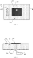
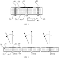
- FIG. 1 illustrates a schematic view of a top view structure of an antenna device provided in embodiments of the present application
- FIG. 2 illustrates a schematic view of an A-A cross-sectional view of an antenna device provided in embodiments of the present application
- the antenna device includes a dielectric substrate 10, a grounding metal layer 20, a radiation patch 30, a first feeding structure 40, a first deflection patch 50, and a radio frequency chip 60.
- the dielectric substrate 10 may include at least one substrate layer, that is to say, the dielectric substrate 10 may include one substrate layer, two substrate layers, three substrate layers, or more than three substrate layers.
- the dielectric substrate 10 includes a first side and a second side opposite to the first side.
- the grounding metal layer 20, the dielectric substrate 10 and the radiation patch 30 are stacked.
- the grounding metal layer 20 is attached to the second side of the dielectric substrate 10.
- the radiation patch 30 is attached to the first side of the dielectric substrate 10.
- the first feeding structure 40 penetrates through the dielectric substrate 10.
- the first end of the first feeding structure 40 is connected to the radiation patch 30, which defines a first connection point between the first feeding structure 40 and the radiation patch 30.
- the second end of the first feeding structure40 extends through the grounding metal layer 20, and is electrically connected to the radio frequency chip 60.
- a first gap is formed between the first feeding structure 40 and the grounding metal layer 20.
- the radio frequency chip 60 is used to feed a first excitation signal to the first feeding structure 40, and the first excitation signal is used to excite the radiation patch 30 to radiate beam.
- the first deflection patch 50 is fixed at the first side of the dielectric substrate 10 away from the grounding metal layer 20.
- the first deflection patch 50 is positioned at a first side of the radiation patch 30.
- the first deflection patch 50 can be converted from an amorphous state to a crystalline state, or from a crystalline state to an amorphous state.
- the first excitation signal can be fed through the first feeding structure 40, and then the radiation patch 30 can be excited by the first excitation signal to radiate the beam, so as to implement the basic function of the antenna device.
- the first deflection patch 50 can be converted from a crystalline state (metal state) to an amorphous state (insulating state), or from an amorphous state (insulating state)to a crystalline state (metal state), so that when the radiation patch 30 radiates beam, the first deflection patch 50 can be controlled to be in different states, that is, the first deflection patch 50 can be controlled to be in a crystalline state, or the first deflection patch 50 can be controlled to be in an amorphous state, so as to implement the deflection of the radiation direction of the beam, thus achieving the adjustment of the radiation direction of the beam, improves the spatial coverage of the antenna device.
- the radiation direction of the beam radiated by the radiation patch 30 excited by the first excitation signal can be deflected to one side of the first deflection patch 50.
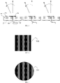
- the radiation direction of the beam radiated by the radiation patch 30 excited by the first excitation signal will not be deflected. That is, as shown in FIG. 3 , when the first deflection patch 50 is in the crystalline state, the beam radiated by the radiation patch 30 is deflected to the first side of the radiation patch 30, as shown in FIG. 4 , when the first deflection patch 50 is in the amorphous state, the beam radiated by the radiation patch 30 does not occur deflection. In this way, the adjustment of multiple radiation directions of the beam of the antenna device can be implemented under different requirements.
- the first connection point between the first feeding structure 40 and the radiation patch 30 may be located on the center line of the radiation patch 30, and a distance between the first connection point and the center point of the radiation patch 30 may be located within a first distance threshold range
- the first distance threshold range refers to a distance range used to adjust impedance matching. That is, the impedance of the antenna device can be adjusted by adjusting the distance between the first connection point and the center point of the radiating patch 30, and then the antenna matching of the antenna device can be implemented to increase radiation efficiency of the antenna device.
- the first connection point can be located on the center line of the radiation patch 30 parallel to the length direction of the first deflection patch 50. Obviously, the first connection point can also be slightly offset from center line of the radiation patch 30 parallel to the length direction of the first deflection patch 50, which is not limited in the present application.
- the distance between the first connection point and the center point of the radiation patch 30 can be adjusted so that the impedance of the antenna device is 4 ohms, 5 ohms, or 6 ohms.
- the present application does not limit the impedance of the antenna device after adjustment.
- the antenna device including the dielectric substrate 10, the grounding metal layer 20, the radiation patch 30, and the first feeding structure 40
- the antenna device may be a side-fire antenna or an end-fire antenna, such as a dipole antenna etc.
- the antenna device, including the dielectric substrate 10, the grounding metal layer 20, the radiation patch 30, and the first feeding structure 40 may be a single antenna unit or an antenna array. That is, the antenna device, including the dielectric substrate 10, the grounding metal layer 20, the radiation patch 30, and the first feeding structure 40, can be arranged in a matrix structure to obtain an antenna array.
- the implementation form of the antenna device, including the dielectric substrate 10, the grounding metal layer 20, the radiation patch 30 and the first feeding structure 40 is not limited in the present application.
- the array antenna formed by the antenna device can not only realize the general performance of the antenna, but also realize the performance of beam scanning.
- the antenna device includes the dielectric substrate 10, the grounding metal layer 20, the radiation patch 30, the first feeding structure 40 and the first deflection patch 50
- the first deflection patch 50 can be controlled to convert from an amorphous state to a crystalline state, and the beam scanning is realized by the antenna array formed by the antenna device, and the beam scanning diagram can be as shown in FIG. 5 .
- the radiation patch 30 may include at least one radiation sub-patch.
- the radiation patch 30 includes two or more radiation sub-patches 301, the radiation sub-patches 301 are stacked, the shape and size of each radiation sub-patch 301 are different from that of the others, or, the shape or size of each radiation sub-patch 301 is different from that of the others. Since each radiation sub-patch 301 has a different shape and size, or, each radiation sub-patch 301 has a different shape or size, when the radiation sub-patches 301 are stacked and arranged, different bandwidths corresponding to each radiation sub-patch 301 and mutual coupling between two radiation sub-patches 301 can increase the overall bandwidth of the radiation patch 30, thereby increasing the bandwidth of the antenna device.
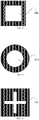
- FIG. 6 and FIG. 7 illustrate some embodiments of the radiation sub-patch 301
- the radiation sub-patch 301 may have a rectangular or circular structure.
- the length direction of the first deflection patch 50 is parallel to the first side of the radiation sub-patch 301, wherein the first side edge of the radiation sub-patch is an edge of the radiation sub-patch adjacent to the first deflection patch 50.
- the length direction of the first deflection patch 50 and the adjacent first side of the radiation sub-patch 301 may define a certain angle.
- the length directions of the first deflection patch 50 and the radiation sub-patch 301 are located on the same plane.
- the radiation sub-patch 301 may be a whole-piece structure, obviously, it also be a sheet-like structure provided with through holes.
- the radiation sub-patch 301 may be a rectangular ring structure, or as shown in FIG. 9 , the radiation sub-patch 301 may be a circular ring structure, or as shown in FIG. 10 , the radiation sub-patch 301 may be a rectangular structure provided with a cross-shaped through hole or the like.
- the first deflection patch 50 may be a striped rectangular structure, and the first deflection patch 50 may be formed by a reversible phase change material.
- the phase change material may be vanadium dioxide, germanium antimony tellurium alloy, scandium antimony tellurium alloy or germanium antimony alloy, etc.
- the first deflection patch 50 and the radiation patch 30 may be located on different substrate layers of the dielectric substrate 10, that is, dielectric substrate 10 may include a first substrate layer and a second substrate layer, at this time, the first deflection patch 50 is fixed on the first substrate layer of the dielectric substrate, and the radiation patch layer 30 is fixed on the second substrate layer of the dielectric substrate; or the first deflection patch 50 is fixed on the second substrate layer of the dielectric substrate, and the radiation patch 30 is fixed on the first substrate layer of the dielectric substrate.
- the first deflection patch 50 and the radiation patch 30 may be located on same substrate layer of the dielectric substrate, that is, the first deflection patch 50 and the radiation patch 30 are located at the same plane. In this way, the deflection effect of the first deflection patch 50 on the direction of the beam of the radiation patch 30 can be better improved.
- the distance between the first deflection patch 50 and the radiation patch 30 approaches zero, the radiation patch 30 and the first deflection patch 50 can be approximated as one piece so that the deflection of the beam radiation direction cannot be achieved; when the distance between the first deflection patch 50 and the radiation patch 30 approaches infinity, it is equivalent to the absence of the first deflection patch 50, so that the deflection of the beam radiation direction cannot be achieved. Therefore, the distance between the first deflection patch 50 and the radiation patch 30 is within a certain range, so as to better realize the deflection of the beam direction radiated by the radiation patch 30.
- the distance between the radiation patch 30 and the first deflection patch 50 may be in a range of about 0.2mm to about 2mm.
- the first deflection patch 50 can switch between the crystalline state and the amorphous state under the action of temperature, obviously, it can also switch between the crystalline state and the amorphous in other ways, such as under the action of laser excitation, the crystalline state and the amorphous state can be switched.
- the antenna device may further include a first conductive structure 70, and the first conductive structure 70 penetrates through the dielectric substrate 10, the first end of the first conductive structure 70 is connected to the first deflection patch 50, and the second end of the first conductive structure 70 extends through the grounding metal layer 20, and is electrically connected to an external circuit, the first conductive structure 70 is insulated from the grounding metal layer 20, and the external circuit is used to feed a first electrical signal to the first conductive structure 70, the first electrical signal is used to excite the first deflection patch 50 from an amorphous state to a crystalline state, or from a crystalline state to an amorphous state.
- the first reflection patch 50 can be excited by the first electrical signal to heat up, when the temperature of the deflection patch 50 is not less than the temperature threshold, the excitation of the first electrical signal is stopped to achieve the rapid cooling of the first deflection patch 50, so that the first deflection patch 50 is switched to the amorphous state.
- the first reflection patch 50 can be excited by the first electrical signal to heat up, when the temperature of the first deflection patch 50 is not less than the temperature threshold, the first electrical signal is slowly reduced to achieve the slow cooling of the first deflection patch 50, so that the first deflection patch 50 is switched to the crystalline state.
- the temperature threshold may be determined based on the material of the first deflection patch 50, and the temperature threshold refers to the temperature at which the crystal grains inside the first deflection patch 50 can be in a free state.
- the antenna device may further include a second deflection patch 80.
- the second deflection patch 80 is located on a second side of the radiation patch 30 opposite to the first side of the radiation patch 30, and the second deflection patch 80 can be converted from an amorphous state to a crystalline state, or from a crystalline state to an amorphous state.
- the second deflection patch 80 is fixed on the first side of the first substrate layer of the dielectric substrate 10 away from the grounding metal layer 20.
- the first deflection patch 50 and the second deflection patch 80 can be located on the same substrate layer of the dielectric substrate.
- the first deflection patch 50 and the second deflection patch 80 can be located on the different substrate layers of the dielectric substrate 10, for example, the first deflection patch 50 is fixed on the first substrate layer, and the second deflection patch 80 is fixed on the second substrate layer of the dielectric substrate 10 away from the grounding metal layer 20, the second substrate layer of the dielectric substrate is a substrate layer of the dielectric substrate 10 which is different from the first substrate layer of the dielectric substrate 10.
- the material of the second deflection patch 80 and the material of the first deflection patch 50 may be the same or similar.
- the setting position of the second deflection patch 80 may be substantially the same or similar to the setting position of the first deflection patch 50. This will not be repeated in the application embodiments.
- the first substrate layer of the dielectric substrate may be located above the second substrate layer of the dielectric substrate, or may be located below the second substrate layer of the dielectric substrate, which is not limited in the embodiment of the present application.
- the first deflection patch 50 and the second deflection patch 80 are both located on the first substrate layer of the dielectric substrate, it can be considered that the first deflection patch 50 and the second deflection patch 80 are arranged in the same layer, when the first deflection patch 50 is located on the first substrate layer of the dielectric substrate and the second deflection patch 80 is located on the second substrate layer of the dielectric substrate, it can be considered that the first deflection patch 50 and the second deflection patch 80 are arranged in different layers.
- the radiation patch 30 may be provided in the same layer as the first deflection patch 50 and the second deflection patch 80, or may be provided in different layers, which is not limited in the embodiment of the present application.
- the antenna device may further include a second conductive structure 90, and the location structure of the second conductive structure 90 may be the same or similar to that of the first conductive structure 70, which will not be repeated in the embodiment of the present application.
- the first deflection patch 50 can be controlled to be converted from an amorphous state to a crystalline state
- the second deflection patch 80 can be controlled to be converted from a crystalline amorphous state to an amorphous state to achieve a beam scan by an antenna array of the antenna device, and the beam scanning diagram can be as shown in FIG. 14
- the first deflection patch 50 can be controlled to be converted from crystalline state to amorphous state
- the second deflection patch 80 is controlled to be converted from an amorphous state to a crystalline state to achieve a beam scan by an antenna array c of the antenna device, and the beam scanning diagram can be as shown in FIG. 15 .
- the antenna device may further include a second feeding structure 11, and the second feeding structure 11 penetrates through the dielectric substrate 10, and the first end of the second feeding structure 11 is electrically connected to the radiation patch 30, and the second end of the second feeding structure 11 extends through the grounding metal layer 20, and is electrically connected to the radio frequency chip 60.
- a second gap is formed between the second feeding structure 11 and the grounding metal layer 20, and the radio frequency chip 60 is used to feed a second excitation signal to the second feeding structure 11, and the second excitation signal is used to excite the radiation patch 30 to radiate radiation beam.
- the radio frequency chip 60 feeds the second excitation signal to the second feeding structure 11
- the radiation patch 30 can be excited by the second excitation signal to radiate the directional beam
- the radio frequency chip 60 can feed the first excitation signal to the first feeding structure 40, under the influence of the first deflection patch 50, the feeding structure 40 excites the beam with adjustable radiation direction of the radiation patch 30 through the first excitation signal.
- the second feeding structure 11 may be provided when the antenna device includes the radiation patch 30 and the first deflection patch 50, or the second feeding structure 11 may be provided when the antenna device includes radiation patch 30, the first deflection patch 50 and the second deflection patch 80.
- a third deflection patch 12 may be further provided when the antenna device includes the radiation patch 30, the first deflection patch 50, and the second feeding structure 11.
- the third deflection patch 12 may also be provided when the antenna device includes the radiation patch 30, the first deflection patch 50, the second deflection patch 80, and the second feeding structure 11.
- the antenna device includes the third deflection patch 12, and the third deflection patch 12 is located at a third side of the radiation patch 30 opposite to the first side of the radiation patch 30, and the third deflection patch 12 can be converted from an amorphous state to a crystalline state, or from a crystalline state to an amorphous state.
- the third deflection patch 12 is fixed on the side of the first substrate layer of the dielectric substrate or the third substrate layer of the dielectric substrate away from the grounding metal layer 20, that is, the first deflection patch 50, the second deflection patch 80, and the third deflection patch 12 are located on the same substrate layer of the dielectric substrate, or the first deflection patch 50 and the second deflection patch 80 are located on the same substrate layer of the dielectric substrate, and the third deflection patch 12 is located on another layer of dielectric substrate.
- the third deflection patch 12 can be controlled to be in different states, that is, the third deflection patch 12 can be controlled to be in a crystalline state, or the third deflection patch 12 can be controlled to be in an amorphous state, so as to implement the deflection of the radiation direction of the beam.
- the radiation direction of the beam radiated by the radiation patch 30 excited by the second excitation signal can be deflected to towards the side where the third deflection patch 12 is located, that is, towards the third side of the third radiation patch; when the third deflection patch 12 is in the amorphous state, the radiation direction of the beam radiated by the radiation patch 30 excited by the second excitation signal will not be deflected. In this way, the adjustment of multiple radiation directions of the beam of the antenna device can be implemented under different requirements.
- the positional relationship between the first substrate layer of the dielectric substrate and the third substrate layer of the dielectric substrate may not be limited, and the first deflection patch 50, the second deflection patch 80, and the third deflection patch 12 may be located on the same substrate layer of the dielectric substrate or on the different substrate layers of the dielectric substrate based on the set position, which are not limited in the embodiment of the present application.
- the third deflection patch 12 may be a striped rectangular structure.
- the material of the third deflection patch 12 may be the same or similar to the material of the first deflection patch 50 described above, and the switching ways of the third deflection patch 12 between the crystalline state and the amorphous state can be referred to the above description, which will not be repeated in the embodiment of the present application.
- the third deflection patch 12 and the radiation patch 30 may be located on the different layers of the dielectric substrate, that is, dielectric substrate 10 comprises at least a third substrate layer of the dielectric substrate and a fourth substrate layer of the dielectric substrate.
- the third deflection patch 12 is fixed on the third substrate layer of the dielectric substrate, and the radiation patch 30 is fixed on the fourth substrate layer of the dielectric substrate; or the third deflection patch 12 is fixed on the fourth substrate layer of the dielectric substrate, and the radiation patch 30 is fixed on the third substrate layer of the dielectric substrate, etc.
- the third deflection patch 12 and the radiation patch 30 may be located on the same substrate layer of the dielectric substrate, that is, the third deflection patch 12 and the radiation patch 30 may be located on the same plane. In this way, the deflection of the direction of the beam radiated by the radiation patch 30 by the third deflection patch 12 can be better improved.
- the antenna device may further include the third conductive structure 13, and the third conductive structure 13 penetrates through the dielectric substrate 10, the first end of the third conductive structure 13 is connected to the third deflection patch 12, and the second end of the third conductive structure 13 extends through the grounding metal layer 20, and is electrically connected to an external circuit, the third conductive structure 13 is insulated from the grounding metal layer 20, and the external circuit is used to feed a third electrical signal to the third conductive structure 13, the third electrical signal is used to excite the third deflection patch 12 from an amorphous state to a crystalline state, or from a crystalline state to an amorphous state.
- the third signal is used to excite the third deflection patch 12 from the amorphous state to the crystalline state, or from the crystalline state to the amorphous state, refer to the above mentioned the first deflection patch 50 is converted from the amorphous state to the realization state, or from the crystalline state to the amorphous state, which will not be repeated in the embodiment of the present application.
- the antenna device may further include a fourth deflection patch 14.
- the fourth deflection patch 14 is located on a fourth side of the radiation patch 30 opposite to the third side of the radiation patch 30, and the fourth deflection patch 14 can be converted from the amorphous state to the crystalline state, or from the crystalline state to the amorphous state.
- the fourth deflection patch 14 is fixed on the side of the first substrate layer of the dielectric substrate or the fourth substrate layer of the dielectric substrate away from the grounding metal layer 20, that is, the first deflection patch 50, the second deflection patch 80, the third deflection patch 12, and the fourth deflection patch 14 are located on the same substrate layer of the dielectric substrate, or the first deflection patch 50, the second deflection patch 80, and the third deflection patch 12 are located on the same substrate layer of the dielectric substrate, and the fourth deflection patch 14 is located on another layer of dielectric substrate.
- the fourth dielectric substrate is one substrate layer of the dielectric substrate of at least one dielectric substrate 10 that is different from the first dielectric substrate.
- the fourth deflection patch 14 is fixed on the side of the third substrate layer of the dielectric substrate away from the grounding metal layer 20; that is, the first deflection patch 50 and the second deflection patch 80 are located on the same substrate layer of the dielectric substrate, and the third deflection patch 12 and the fourth deflection patch 14 are located on the same substrate layer of the dielectric substrate.
- the positional relationship between the first substrate layer of the dielectric substrate, the second substrate layer of the dielectric substrate, the third substrate layer of the dielectric substrate, and the fourth substrate layer of the dielectric substrate may not be limited, and the first deflection patch 50, the second deflection patch 80, the third deflection patch 12 and the fourth deflection patch 14 may be located on the same layer of dielectric substrate or on the different layers of the dielectric substrate based on the set position, which are not limited in the embodiment of the present application.
- the material of the fourth deflection patch 14 and the material of the third deflection patch 12 may be the same or similar.
- the setting position of the fourth deflection patch 14 may be substantially the same or similar to the setting position of the third deflection patch 12. This will not be repeated in the application embodiment.
- the antenna device may further include a fourth conductive structure 15, and the location structure of the fourth conductive structure 15 may be the same or similar to that of the third conductive structure 13, which will not be repeated in the embodiment of the present application.
- the antenna device includes a third deflection patch 12
- the third deflection patch 12 is fixed on the side of the first substrate layer of the dielectric substrate or the third substrate layer of the dielectric substrate away from the grounding metal layer 20
- the third substrate layer of the dielectric substrate is one substrate layer of the dielectric substrate of at least one dielectric substrate 10 that is different from the first dielectric substrate and the second dielectric substrate.
- first deflection patch 50 and the third deflection patch 12 are located on the same substrate layer of the dielectric substrate, and the second deflection patch 80 is located on another substrate layer of the dielectric substrate; or the first deflection patch 50, the second deflection patch 80, and the third deflection patch 12 are located on the different layers of the dielectric substrate.
- the fourth deflection patch 14 is located on the fourth side of the radiation patch opposite to the third side of the radiation patch 30, and the fourth deflection patch 14 can be converted from the amorphous state to the crystalline state, or from the crystalline state to the amorphous state.
- the fourth deflection patch 14 is fixed on the side of the second substrate layer of the dielectric substrate away from the grounding metal layer 20; that is, the first deflection patch 50 and the third deflection patch 12 are located on the same substrate layer of the dielectric substrate, and the second deflection patch 80 and the fourth deflection patch 14 are located on the same substrate layer of the dielectric substrate.
- the fourth deflection patch 14 is fixed on the side of the first substrate layer of the dielectric substrate, the third substrate layer of the dielectric substrate, or the fourth substrate layer of the dielectric substrate away from the grounding metal layer 20, that is, the first deflection patch 50, the second deflection patch 80, and the third deflection patch 12 are located on the different layers of the dielectric substrate, and the fourth deflection patch 14 and the first deflection patch 50 are located on the same layer; or the first deflection patch 50, the second deflection patch 80, and the third deflection patch 12 are located on the different layers of the dielectric substrate, and the fourth deflection patch 14 and the third deflection patch 12 are located on the same layer; or the first deflection patch 50, the second deflection patch 80, the third deflection patch 12 and the fourth deflection patch 14 are located on the different layers of the dielectric substrate.
- the antenna device when the antenna device includes a first deflection patch 50, a second deflection patch 80, a third deflection patch 12, and a fourth deflection patch 14, the first deflection patch 50, the second bias
- the sheet 80, the third deflection patch 12, the fourth deflection patch 14 and the radiation patch 30 can be fixed to the same substrate layer of the dielectric substrate, that is, the first deflection patch 50, the second deflection patch 80, the third deflection patch 12, the fourth deflection patch 14, and the radiation patch 30 may be located one the same plane, which is not limited in the embodiment of the present application.
- any one of the first deflection patch 50, the second deflection patch 80, the third deflection patch 12, and the fourth deflection patch 14 can be controlled to change from a crystalline state to an amorphous state, or from an amorphous state to a crystalline state, so as to achieve the scanning of the radiation beam of the antenna array formed by this antenna device.
- the beam scanning diagram thereof may be referred to the scanning diagram when only the first deflection patch 50 and the second deflection patch 80 are included, which is not limited in the embodiment of the present application.
- the fourth deflection patch 14 when the second feeding structure 11 feeds the excitation signal, the fourth deflection patch 14 is in a crystalline state, and the third deflection patch 12 is in an amorphous state, regardless of the state of the first deflection patch 50 and the second deflection patch 80, the main beam of the antenna is deflected in the direction of the fourth deflection patch 14.
- the fourth deflection patch 14 is in an amorphous state
- the third deflection patch 12 is in a crystalline state, regardless of the state of the first deflection patch 50 and the second deflection patch 80, the main beam of the antenna is deflected in the direction of the third deflection patch 12.
- the main beam of the antenna is not deflected, usually in the side firing direction.
- the first deflection patch 50 is in a crystalline state
- the second deflection patch 80 is in an amorphous state, regardless of the state of the fourth deflection patch 14 and the third deflection patch 12, the main beam of the antenna is deflected in the direction of the first deflection patch 50.
- the first deflection patch 50 When the first feeding structure 40 feeds the excitation signal, the first deflection patch 50 is in an amorphous state, and the second deflection patch 80 is in a crystalline state, regardless of the state of the fourth deflection patch 14 and the third deflection patch 12, the main beam of the antenna is deflected in the direction of the second deflection patch 50. And, when the first feeding structure 40 feeds the excitation signal, the first deflection patch 50 and the second deflection patch 80 are in the same state, the main beam of the antenna is not deflected, usually in the end firing direction.
- the single-polarized antenna may be formed by the first feeding structure 40 and the radiation patch 30, obviously, the antenna device may further include a third feeding structure, and the third feeding structure penetrates through the dielectric substrate 10, and the first end of the third feeding structure is connected to the radiation patch 30, the second end of the third feeding structure extends through the grounding metal layer 20, a third gap is formed between the third feeding structure and the grounding metal layer 20.
- the third feeding is used to feed the third excitation signal, and the third excitation signal is used to excite the radiation patch 30 to radiate beam.
- the dual-polarized antenna can be realized, and thus the deflection of the beam radiation direction of the dual-polarized antenna can be achieved by the first deflection patch 50.
- a third connection point between the third feeding structure and the radiation patch 30 and the first connection point form center symmetry with the center point of the radiation patch 30.
- the single-polarized antenna may be formed by the second feeding structure 11 and the radiation patch 30, obviously, the antenna device may further include a fourth feeding structure, and the fourth feeding structure penetrates through the dielectric substrate 10, and the first end of the fourth feeding structure is connected to the radiation patch 30, the second end of the fourth feeding structure extends through the grounding metal layer 20, and is electrically connected to the radio frequency chip 60. A fourth gap is formed between the fourth feeding structure and the grounding metal layer 20.
- the fourth feeding structure is used to feed the fourth excitation signal, and the fourth excitation signal is used to excite the radiation patch 30 radiation beam.
- the dual-polarized antenna can be realized, and thus the deflection of the beam radiation direction of the dual-polarized antenna can be achieved by the third deflection patch 12 and the fourth deflection patch 14.
- the fourth connection point between the fourth feeding structure and the radiation patch 30 and the second connection point form center symmetry with the center point of the radiation patch 30.
- the first excitation signal and the second excitation signal can be fed through the first feeding structure and the second feeding structure respectively, and then the radiation patch can be excited by the first excitation signal and the second excitation signal to radiate the beam, so as to implement the basic function of the antenna device.
- first deflection patch, the second deflection patch, the third deflection patch, and the fourth deflection patch can all be converted from a crystalline state (metal state) to an amorphous state (insulating state), or from an amorphous state (insulating state)to a crystalline state (metal state), so that when the radiation patch radiation beam is excited by the first excitation signal and the second excitation signal, the first deflection patch and the second deflection patch can be controlled to be in different states, and the third deflection patch and the fourth deflection patch can be controlled to be in different states.
- the first deflection patch can be controlled to be in the crystalline state and the second deflection patch can be controlled to be in the amorphous state, or, the first deflection patch is in the amorphous state, and the second deflection patch is in the crystalline state, and the third deflection patch can be controlled to be in the crystalline state and the fourth deflection patch can be controlled to be in the amorphous state, or the third deflection patch is in the amorphous state and the fourth deflection patch is in the crystalline state, thus achieving the adjustment of the radiation direction of the beam, improves the spatial coverage of the antenna device.
- FIG. 18 illustrates a schematic structural view of an electronic device according to an embodiment of the present application.
- the electronic device may include the antenna device described in the above embodiments.
- the electronic device may be a smart phone, a tablet computer, an MP3 player (Moving Picture Experts Group Audio Layer III, Dynamic Image Expert Compression Standard Audio 3), MP4 player (Moving Picture Experts Group Audio Layer IV, Dynamic Image Expert Compression Standard Audio 4), a laptop or a desktop computer, etc.
- MP3 player Moving Picture Experts Group Audio Layer III, Dynamic Image Expert Compression Standard Audio 3
- MP4 player Moving Picture Experts Group Audio Layer IV, Dynamic Image Expert Compression Standard Audio 4
- a laptop or a desktop computer etc.
- the electronic device may include a housing 1801in which a processor 1802, a memory 1803, a controller 1804, and the antenna device 1805 of the embodiments shown in FIG. 1 to FIG. 17 .
- the processor 1802 may include one or more processing cores, such as a four-core processor, eight-core processor, and so on.
- the memory 1803 may include one or more computer-readable storage media, which may be non-transitory.
- the controller 1804 is used to control the first deflection patch to be converted from an amorphous state to a crystalline state, or from a crystalline state to an amorphous state, obviously, when the antenna device includes other deflection patches, the controller 1804 can also be used to control other deflection patches to be converted from an amorphous state to a crystalline state, or from a crystalline state to an amorphous state.
- the antenna device 1805 is used to receive electromagnetic signals, and convert them into electromagnetic wave signals to communicate with communication networks and other communication devices, or to convert the received electromagnetic wave signals into electromagnetic signals.
- the electromagnetic wave signal may be millimeter wave signal or Sub-6GHz signal, etc., which is not limited in the embodiment of the present application.
- FIG. 18 does not constitute a limitation on the electronic device, and the electronic device may include more or fewer components than those shown in the diagram, or combine certain components, or adopt different component arrangements.
- the antenna device can achieve deflection of the beam radiation direction under the action of the first deflection patch, the spatial coverage of the antenna device is improved to ensure the performance of the antenna device. In this way, it is possible to increase the spatial coverage of radiation by beam radiation in different directions of the multiple antenna devices arranged inside the electronic device, so as to improve the antenna performance of the electronic device.
Landscapes
- Variable-Direction Aerials And Aerial Arrays (AREA)
- Waveguide Aerials (AREA)
Abstract
Description
- This application is claims priority to
Chinese Patent Application No. 202010195147.6 filed on March 19, 2020 - The present application relates to the field of antenna technology, and in particular to an antenna device and an electronic device.
- During the use of electronic devices, in order to ensure antenna performance of the electronic device, the antenna device is fixedly installed. Due to the fixed arrangement of the antenna device, the radiation direction of the beam of the antenna device is fixed.
- The application provides an antenna device and an electronic device. The technical solution is as follows.
- In one aspect, an antenna device includes a dielectric substrate, a grounding metal layer, a radiation patch, a first feeding structure, a first deflection patch, and a radio frequency chip.
- The grounding metal layer, the dielectric substrate, and the radiation patch are stacked; the first feeding structure penetrates through the dielectric substrate; a first end of the first feeding structure is connected to the radiation patch, and a second end of the first feeding structure extends through the grounding metal layer, and is electrically connected to the radio frequency chip; a first gap is formed between the first feeding structure and the grounding metal layer, the radio frequency chip is configured to feed a first excitation signal to the first feeding structure to excite the radiation patch to radiate beam.
- The first deflection patch is fixed on a side of dielectric substrate away from the grounding metal layer, the first deflection patch is located at a side of the radiation patch, the first deflection patch is configured to be in an amorphous state or in a crystalline state when the antenna device works.
- Another aspect provides an electronic device, the electronic device includes a controller and the antenna device as described above, and the controller is used to control the first deflection patch to be converted from an amorphous state to a crystalline state, or from a crystalline state to an amorphous state.
- In order to more clearly describe the technical solution in the embodiments of the present application, the following will be briefly introduce the drawings that need to be used in the description of the embodiments. Apparently, the drawings in the following description are only some embodiments of the present application. For those of ordinary skill in the art, other drawings can be obtained in accordance with these drawings without creative labor.
-
FIG. 1 is a schematic view of a top view structure of an antenna device provided in embodiments of the present application. -
FIG. 2 is a schematic view of a cross-sectional view of the antenna device taken along a line A-A in other embodiments of the present application. -
FIG. 3 is a schematic view of a beam radiation direction when a first deflection patch is in a crystalline state provided in embodiments of the present application. -
FIG. 4 is a schematic view of a beam radiation direction when a first deflection patch is in an amorphous state provided in embodiments of the present application. -
FIG. 5 is a schematic view of beam scanning of an antenna array composed of an antenna device provided in embodiments of the present application. -
FIG. 6 is a schematic structural view of a radiation patch provided in embodiments of the present application. -
FIG. 7 is a schematic structural view of a radiation patch provided in other embodiments of the present application. -
FIG. 8 is a schematic structural view of a radiation patch provided in other embodiments of the present application. -
FIG. 9 is a schematic structural view of a radiation patch provided in other embodiments of the present application. -
FIG. 10 is a schematic structural view of a radiation patch provided in other embodiments of the present application. -
FIG. 11 is a schematic structural view of an antenna device provided in other embodiments of the present application. -
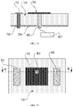
FIG. 12 is a schematic view of a top view structure of an antenna device provided in other embodiments of the present application. -
FIG. 13 is a schematic view of a cross-sectional view of the antenna device taken along a line B-B in other embodiments of the present application. -
FIG. 14 is a schematic view of beam scanning of an antenna array composed of an antenna device provided in other embodiments of the present application. -
FIG. 15 is a schematic view of beam scanning of an antenna array composed of an antenna device provided in other embodiments of the present application. -
FIG. 16 is a schematic view of a top view structure of an antenna device provided in other embodiments of the present application. -
FIG. 17 is a schematic view of a cross-sectional view of an antenna device taken along a line C-C provided in other embodiments of the present application. -
FIG. 18 is a schematic structural view of an electronic device provided in embodiments of the present application. - Reference signs: 10: dielectric substrate; 20: grounding metal layer; 30: radiation patch; 301: radiation sub-patch; 40: first feeding structure; 50: first deflection patch; 60: radio frequency chip; 70: first conductive structure; 80: second deflection patch; 90: second conductive structure; 11: second feeding structure; 12: third deflection patch; 13: third conductive structure; 14: fourth deflection patch; 15: fourth conductive structure;
1801: housing; 1802: processor; 1803: memory; 1804: controller; 1805: antenna device. - In order to make the purpose, technical solutions and advantages of the present application clear, the present application will be further described in detail below with reference to the accompanying drawings.
- The present disclosure provides an antenna device includes a dielectric substrate, a grounding metal layer, a radiation patch, a first feeding structure, a first deflection patch, and a radio frequency chip.
- The grounding metal layer, the dielectric substrate, and the radiation patch are stacked, the first feeding structure penetrates through the dielectric substrate, the first end of the first feeding structure is connected to the radiation patch, and the second end of the first feeding structure extends through the grounding metal layer, and is electrically connected to the radio frequency chip, a first gap is formed between the first feeding structure and the grounding metal layer, and the radio frequency chip is used to feed a first excitation signal to the first feeding structure, and the first excitation signal is used to excite the radiation patch radiate beam.
- The first deflection patch is fixed on the side of the first substrate layer of the dielectric substrate away from the grounding metal layer, the first deflection patch is located on the first side of the radiation patch, the first deflection patch can be converted from an amorphous state to a crystalline state, or from a crystalline state to an amorphous state, and the first substrate layer of the dielectric substrate is any one of the at least one dielectric substrate.
- In an embodiment, when the first deflection patch is in a crystalline state, the beam radiated by the radiation patch is deflected to the first side of the radiation patch.
- In an embodiment, when the first deflection patch is in an amorphous state, the beam radiated by the radiation patch radiation does not deflect.
- In an embodiment, the first deflection patch achieves conversion between the crystalline state and the amorphous states under the action of temperature or laser.
- In an embodiment, the antenna device further includes a first conductive structure.
- The first conductive structure penetrates through the dielectric substrate, and the first end of the first conductive structure is connected to the first deflection patch, and the second end of the first conductive structure extends through the grounding metal layer, and is electrically connected to an external circuit, the first conductive structure is insulated from the grounding metal layer, the external circuit is used to feed a first electrical signal to the first conductive structure, the first electrical signal is used to excite the first deflection patch from an amorphous state to a crystalline state, or from a crystalline state to an amorphous state.
- In an embodiment, the distance between the radiation patch and the first deflection patch is greater than or equal to 0.2 mm and less than or equal to 2 mm.
- In an embodiment, the antenna device further includes a second deflection patch.
- The second deflection patch is fixed on the side of the first substrate layer of the dielectric substrate away from the grounding metal layer.
- The second deflection patch is located on the second side of the radiation patch opposite to the first side, the second deflection patch can be converted from an amorphous state to a crystalline state, or from a crystalline state to an amorphous state.
- In an embodiment, the antenna device further includes a second deflection patch.
- The second deflection patch is fixed on the side of the second substrate layer of the dielectric substrate away from the grounding metal layer.
- The second deflection patch is located on the second side of the radiation patch opposite to the first side, the second deflection patch can be converted from an amorphous state to a crystalline state, or from a crystalline state to an amorphous state. The second substrate layer of the dielectric substrate is a substrate layer of the dielectric substrate which is different from the first substrate layer of the dielectric substrate in the dielectric substrate.
- In an embodiment, the antenna device further includes a second feeding structure.
- The second feeding structure penetrates through the dielectric substrate, the first end of the second feeding structure is electrically connected to the radiation patch, and the second end of the second feeding structure extends through the grounding metal layer, and is electrically connected to the radio frequency chip, a second gap is formed between the second feeding structure and the grounding metal layer, and the radio frequency chip is used to feed a second excitation signal to the second feeding structure, and the second excitation signal is used to excite the radiation patch radiation beam.
- In an embodiment, the antenna device further includes a third deflection patch.
- When the second deflection patch is fixed on the side of the first substrate layer of the dielectric substrate away from the grounding metal layer, the third deflection patch is fixed on the side of the first substrate layer of the dielectric substrate or the third layer of the dielectric away from the grounding metal layer. The third substrate layer of the dielectric substrate is a substrate layer of the dielectric substrate which is different from the first substrate layer of the dielectric substrate in the dielectric substrate.
- The third deflection patch is located on the third side of the radiation patch adjacent to the first side, and the third deflection patch can be converted from an amorphous state to a crystalline state, or from a crystalline state to an amorphous state.
- In an embodiment, the antenna device further includes a fourth deflection patch.
- When the third deflection patch is fixed on the side of the first substrate layer of the dielectric substrate away from the grounding metal layer, the fourth deflection patch is fixed on the side of the first substrate layer of the dielectric substrate or the fourth substrate layer of the dielectric substrate away from the grounding metal layer. The fourth substrate layer of the dielectric substrate is a substrate layer of the dielectric substrate which is different from the first substrate layer of the dielectric substrate in the dielectric substrate.
- The fourth deflection patch is located on the fourth side of the radiation patch opposite the third side, the fourth deflection patch can be converted from an amorphous state to a crystalline state.
- In an embodiment, the antenna device further includes a fourth deflection patch.
- When the third deflection patch is fixed on the side of the third substrate layer of the dielectric substrate away from the grounding metal layer, the fourth deflection patch is fixed on the side of the third substrate layer of the dielectric substrate away from the grounding metal layer.
- The fourth deflection patch is located on the fourth side of the radiation patch opposite the third side, the fourth deflection patch can be converted from an amorphous state to a crystalline state.
- In an embodiment, the antenna device further includes a third deflection patch.
- When the second deflection patch is fixed on the side of the second substrate layer of the dielectric substrate away from the grounding metal layer, the third deflection patch is fixed on the side of the first substrate layer of the dielectric substrate or the third substrate layer of the dielectric substrate away from the grounding metal layer. The third substrate layer of the dielectric substrate is a substrate layer of the dielectric substrate which is different from the first substrate layer of the dielectric substrate and the second substrate layer of the dielectric substrate in the dielectric substrate.
- The third deflection patch is located on the third side of the radiation patch adjacent to the first side, and the third deflection patch can be converted from an amorphous state to a crystalline state, or from a crystalline state to an amorphous state.
- In an embodiment, the antenna device further includes a fourth deflection patch.
- When the third deflection patch is fixed on the side of the first substrate layer of the dielectric substrate away from the grounding metal layer, the fourth deflection patch is fixed on side of the second substrate layer of the dielectric substrate away from the grounding metal layer.
- The fourth deflection patch is located on the fourth side of the radiation patch opposite the third side, the fourth deflection patch can be converted from an amorphous state to a crystalline state.
- In an embodiment, the antenna device further includes a fourth deflection patch.
- When the third deflection patch is fixed on the side of the third substrate layer of the dielectric substrate away from the grounding metal layer, the fourth deflection patch is fixed on the side of the first substrate layer of the dielectric substrate, the third substrate layer of the dielectric substrate or the fourth substrate layer of the dielectric substrate away from the grounding metal layer. The fourth substrate layer of the dielectric substrate is a substrate layer of the dielectric substrate which is different from the first substrate layer of the dielectric substrate, the second substrate layer of the dielectric substrate and the third substrate layer of the dielectric substrate in the dielectric substrate.
- The fourth deflection patch is located on the fourth side of the radiation patch opposite the third side, the fourth deflection patch can be converted from an amorphous state to a crystalline state.
- In an embodiment, the radiation patch includes two or more radiation sub-patches, the sub-radiation patches are stacked, the shape and size of each radiation sub-patch are different from that of the others, or, the shape or size of each radiation sub-patch are different from that of the others.
- In an embodiment, the radiation sub-patch has a rectangular or circular structure.
- In an embodiment, the antenna device is a side-fire antenna or an end-fire antenna.
- In an embodiment, the antenna device comprises a single antenna element or an antenna array.
- An embodiment of the present application provides an electronic device, the electronic device includes a controller and the antenna device which is illustrated in any of the above embodiments. And the controller is used to control the first deflection patch to be converted from an amorphous state to a crystalline state, or from a crystalline state to an amorphous state.
-
FIG. 1 illustrates a schematic view of a top view structure of an antenna device provided in embodiments of the present application, andFIG. 2 illustrates a schematic view of an A-A cross-sectional view of an antenna device provided in embodiments of the present application. As shown inFIG. 1 and FIG. 2 , the antenna device includes adielectric substrate 10, a groundingmetal layer 20, aradiation patch 30, afirst feeding structure 40, afirst deflection patch 50, and aradio frequency chip 60. Thedielectric substrate 10 may include at least one substrate layer, that is to say, thedielectric substrate 10 may include one substrate layer, two substrate layers, three substrate layers, or more than three substrate layers. Thedielectric substrate 10 includes a first side and a second side opposite to the first side. The groundingmetal layer 20, thedielectric substrate 10 and theradiation patch 30 are stacked. The groundingmetal layer 20 is attached to the second side of thedielectric substrate 10. Theradiation patch 30 is attached to the first side of thedielectric substrate 10. Thefirst feeding structure 40 penetrates through thedielectric substrate 10. The first end of thefirst feeding structure 40 is connected to theradiation patch 30, which defines a first connection point between thefirst feeding structure 40 and theradiation patch 30. The second end of the first feeding structure40 extends through the groundingmetal layer 20, and is electrically connected to theradio frequency chip 60. A first gap is formed between thefirst feeding structure 40 and the groundingmetal layer 20. Theradio frequency chip 60 is used to feed a first excitation signal to thefirst feeding structure 40, and the first excitation signal is used to excite theradiation patch 30 to radiate beam. Thefirst deflection patch 50 is fixed at the first side of thedielectric substrate 10 away from the groundingmetal layer 20. Thefirst deflection patch 50 is positioned at a first side of theradiation patch 30. Thefirst deflection patch 50 can be converted from an amorphous state to a crystalline state, or from a crystalline state to an amorphous state. - In the embodiment of the present application, the first excitation signal can be fed through the
first feeding structure 40, and then theradiation patch 30 can be excited by the first excitation signal to radiate the beam, so as to implement the basic function of the antenna device. Alternatively, since thefirst deflection patch 50 can be converted from a crystalline state (metal state) to an amorphous state (insulating state), or from an amorphous state (insulating state)to a crystalline state (metal state), so that when theradiation patch 30 radiates beam, thefirst deflection patch 50 can be controlled to be in different states, that is, thefirst deflection patch 50 can be controlled to be in a crystalline state, or thefirst deflection patch 50 can be controlled to be in an amorphous state, so as to implement the deflection of the radiation direction of the beam, thus achieving the adjustment of the radiation direction of the beam, improves the spatial coverage of the antenna device. - In operation, when the
first deflection patch 50 is controlled to be in the crystalline state, the radiation direction of the beam radiated by theradiation patch 30 excited by the first excitation signal can be deflected to one side of thefirst deflection patch 50. When thefirst deflection patch 50 is controlled to be in the amorphous state, the radiation direction of the beam radiated by theradiation patch 30 excited by the first excitation signal will not be deflected. That is, as shown inFIG. 3 , when thefirst deflection patch 50 is in the crystalline state, the beam radiated by theradiation patch 30 is deflected to the first side of theradiation patch 30, as shown inFIG. 4 , when thefirst deflection patch 50 is in the amorphous state, the beam radiated by theradiation patch 30 does not occur deflection. In this way, the adjustment of multiple radiation directions of the beam of the antenna device can be implemented under different requirements. - The first connection point between the
first feeding structure 40 and theradiation patch 30 may be located on the center line of theradiation patch 30, and a distance between the first connection point and the center point of theradiation patch 30 may be located within a first distance threshold range, the first distance threshold range refers to a distance range used to adjust impedance matching. That is, the impedance of the antenna device can be adjusted by adjusting the distance between the first connection point and the center point of the radiatingpatch 30, and then the antenna matching of the antenna device can be implemented to increase radiation efficiency of the antenna device. The first connection point can be located on the center line of theradiation patch 30 parallel to the length direction of thefirst deflection patch 50. Obviously, the first connection point can also be slightly offset from center line of theradiation patch 30 parallel to the length direction of thefirst deflection patch 50, which is not limited in the present application. - Illustratively, the distance between the first connection point and the center point of the
radiation patch 30 can be adjusted so that the impedance of the antenna device is 4 ohms, 5 ohms, or 6 ohms. The present application does not limit the impedance of the antenna device after adjustment. - In some embodiments, the antenna device, including the
dielectric substrate 10, the groundingmetal layer 20, theradiation patch 30, and thefirst feeding structure 40, may be a side-fire antenna or an end-fire antenna, such as a dipole antenna etc. In addition, the antenna device, including thedielectric substrate 10, the groundingmetal layer 20, theradiation patch 30, and thefirst feeding structure 40, may be a single antenna unit or an antenna array. That is, the antenna device, including thedielectric substrate 10, the groundingmetal layer 20, theradiation patch 30, and thefirst feeding structure 40, can be arranged in a matrix structure to obtain an antenna array. The implementation form of the antenna device, including thedielectric substrate 10, the groundingmetal layer 20, theradiation patch 30 and thefirst feeding structure 40, is not limited in the present application. - In some embodiments, because the beam radiation direction of the antenna device can be adjusted, the array antenna formed by the antenna device can not only realize the general performance of the antenna, but also realize the performance of beam scanning. Wherein, when the antenna device includes the
dielectric substrate 10, the groundingmetal layer 20, theradiation patch 30, thefirst feeding structure 40 and thefirst deflection patch 50, thefirst deflection patch 50 can be controlled to convert from an amorphous state to a crystalline state, and the beam scanning is realized by the antenna array formed by the antenna device, and the beam scanning diagram can be as shown inFIG. 5 . - In some embodiments, the
radiation patch 30 may include at least one radiation sub-patch. When theradiation patch 30 includes two ormore radiation sub-patches 301, theradiation sub-patches 301 are stacked, the shape and size of eachradiation sub-patch 301 are different from that of the others, or, the shape or size of eachradiation sub-patch 301 is different from that of the others. Since eachradiation sub-patch 301 has a different shape and size, or, eachradiation sub-patch 301 has a different shape or size, when theradiation sub-patches 301 are stacked and arranged, different bandwidths corresponding to eachradiation sub-patch 301 and mutual coupling between tworadiation sub-patches 301 can increase the overall bandwidth of theradiation patch 30, thereby increasing the bandwidth of the antenna device. -
FIG. 6 and FIG. 7 illustrate some embodiments of theradiation sub-patch 301, theradiation sub-patch 301 may have a rectangular or circular structure. - When the
radiation sub-patch 301 has a rectangular structure, the length direction of thefirst deflection patch 50 is parallel to the first side of theradiation sub-patch 301, wherein the first side edge of the radiation sub-patch is an edge of the radiation sub-patch adjacent to thefirst deflection patch 50. In some alternative embodiments, the length direction of thefirst deflection patch 50 and the adjacent first side of theradiation sub-patch 301 may define a certain angle. - When the
sub-radiating patch 301 has a circular structure, the length directions of thefirst deflection patch 50 and theradiation sub-patch 301 are located on the same plane. - For example, the
radiation sub-patch 301 may be a whole-piece structure, obviously, it also be a sheet-like structure provided with through holes. For example, as shown inFIG. 8 , theradiation sub-patch 301 may be a rectangular ring structure, or as shown inFIG. 9 , theradiation sub-patch 301 may be a circular ring structure, or as shown inFIG. 10 , theradiation sub-patch 301 may be a rectangular structure provided with a cross-shaped through hole or the like. - In an embodiment, as shown in
FIG. 1 , thefirst deflection patch 50 may be a striped rectangular structure, and thefirst deflection patch 50 may be formed by a reversible phase change material. For example, the phase change material may be vanadium dioxide, germanium antimony tellurium alloy, scandium antimony tellurium alloy or germanium antimony alloy, etc. - In some embodiments, the
first deflection patch 50 and theradiation patch 30 may be located on different substrate layers of thedielectric substrate 10, that is,dielectric substrate 10 may include a first substrate layer and a second substrate layer, at this time, thefirst deflection patch 50 is fixed on the first substrate layer of the dielectric substrate, and theradiation patch layer 30 is fixed on the second substrate layer of the dielectric substrate; or thefirst deflection patch 50 is fixed on the second substrate layer of the dielectric substrate, and theradiation patch 30 is fixed on the first substrate layer of the dielectric substrate. - In some embodiments, the
first deflection patch 50 and theradiation patch 30 may be located on same substrate layer of the dielectric substrate, that is, thefirst deflection patch 50 and theradiation patch 30 are located at the same plane. In this way, the deflection effect of thefirst deflection patch 50 on the direction of the beam of theradiation patch 30 can be better improved. - For example, when the distance between the
first deflection patch 50 and theradiation patch 30 approaches zero, theradiation patch 30 and thefirst deflection patch 50 can be approximated as one piece so that the deflection of the beam radiation direction cannot be achieved; when the distance between thefirst deflection patch 50 and theradiation patch 30 approaches infinity, it is equivalent to the absence of thefirst deflection patch 50, so that the deflection of the beam radiation direction cannot be achieved. Therefore, the distance between thefirst deflection patch 50 and theradiation patch 30 is within a certain range, so as to better realize the deflection of the beam direction radiated by theradiation patch 30. - Wherein, the distance between the
radiation patch 30 and thefirst deflection patch 50 may be in a range of about 0.2mm to about 2mm. - In some embodiments, the
first deflection patch 50 can switch between the crystalline state and the amorphous state under the action of temperature, obviously, it can also switch between the crystalline state and the amorphous in other ways, such as under the action of laser excitation, the crystalline state and the amorphous state can be switched. - When the state is switched by the effect of temperature, as shown in
FIG. 11 , the antenna device may further include a firstconductive structure 70, and the firstconductive structure 70 penetrates through thedielectric substrate 10, the first end of the firstconductive structure 70 is connected to thefirst deflection patch 50, and the second end of the firstconductive structure 70 extends through the groundingmetal layer 20, and is electrically connected to an external circuit, the firstconductive structure 70 is insulated from the groundingmetal layer 20, and the external circuit is used to feed a first electrical signal to the firstconductive structure 70, the first electrical signal is used to excite thefirst deflection patch 50 from an amorphous state to a crystalline state, or from a crystalline state to an amorphous state. - In operation, when the
first deflection patch 50 is converted from the amorphous state to the crystalline state, assuming that thefirst deflection patch 50 is currently in the crystalline state, thefirst reflection patch 50 can be excited by the first electrical signal to heat up, when the temperature of thedeflection patch 50 is not less than the temperature threshold, the excitation of the first electrical signal is stopped to achieve the rapid cooling of thefirst deflection patch 50, so that thefirst deflection patch 50 is switched to the amorphous state. And, assuming that thefirst deflection patch 50 is currently in the amorphous state, thefirst reflection patch 50 can be excited by the first electrical signal to heat up, when the temperature of thefirst deflection patch 50 is not less than the temperature threshold, the first electrical signal is slowly reduced to achieve the slow cooling of thefirst deflection patch 50, so that thefirst deflection patch 50 is switched to the crystalline state. - Wherein, the temperature threshold may be determined based on the material of the
first deflection patch 50, and the temperature threshold refers to the temperature at which the crystal grains inside thefirst deflection patch 50 can be in a free state. - In an embodiment, as shown in
FIG. 12 , the antenna device may further include asecond deflection patch 80. Thesecond deflection patch 80 is located on a second side of theradiation patch 30 opposite to the first side of theradiation patch 30, and thesecond deflection patch 80 can be converted from an amorphous state to a crystalline state, or from a crystalline state to an amorphous state. - Wherein, the
second deflection patch 80 is fixed on the first side of the first substrate layer of thedielectric substrate 10 away from the groundingmetal layer 20. Thefirst deflection patch 50 and thesecond deflection patch 80 can be located on the same substrate layer of the dielectric substrate. Alternatively, thefirst deflection patch 50 and thesecond deflection patch 80 can be located on the different substrate layers of thedielectric substrate 10, for example, thefirst deflection patch 50 is fixed on the first substrate layer, and thesecond deflection patch 80 is fixed on the second substrate layer of thedielectric substrate 10 away from the groundingmetal layer 20, the second substrate layer of the dielectric substrate is a substrate layer of thedielectric substrate 10 which is different from the first substrate layer of thedielectric substrate 10. - Wherein, the material of the
second deflection patch 80 and the material of thefirst deflection patch 50 may be the same or similar. In some embodiments, the setting position of the second deflection patch 80may be substantially the same or similar to the setting position of thefirst deflection patch 50. This will not be repeated in the application embodiments. - Wherein, the first substrate layer of the dielectric substrate may be located above the second substrate layer of the dielectric substrate, or may be located below the second substrate layer of the dielectric substrate, which is not limited in the embodiment of the present application. When the
first deflection patch 50 and thesecond deflection patch 80 are both located on the first substrate layer of the dielectric substrate, it can be considered that thefirst deflection patch 50 and thesecond deflection patch 80 are arranged in the same layer, when thefirst deflection patch 50 is located on the first substrate layer of the dielectric substrate and thesecond deflection patch 80 is located on the second substrate layer of the dielectric substrate, it can be considered that thefirst deflection patch 50 and thesecond deflection patch 80 are arranged in different layers. In addition, theradiation patch 30 may be provided in the same layer as thefirst deflection patch 50 and thesecond deflection patch 80, or may be provided in different layers, which is not limited in the embodiment of the present application. - Alternatively, when the reversible change between the crystalline state and the amorphous state of the
second deflection patch 80 is achieved by temperature change, as shown inFIG. 13 , the antenna device may further include a secondconductive structure 90, and the location structure of the secondconductive structure 90 may be the same or similar to that of the firstconductive structure 70, which will not be repeated in the embodiment of the present application. - For example, when the antenna device includes the
first deflection patch 50 and thesecond deflection patch 80, thefirst deflection patch 50 can be controlled to be converted from an amorphous state to a crystalline state, and thesecond deflection patch 80 can be controlled to be converted from a crystalline amorphous state to an amorphous state to achieve a beam scan by an antenna array of the antenna device, and the beam scanning diagram can be as shown inFIG. 14 ; or thefirst deflection patch 50 can be controlled to be converted from crystalline state to amorphous state, and thesecond deflection patch 80 is controlled to be converted from an amorphous state to a crystalline state to achieve a beam scan by an antenna array c of the antenna device, and the beam scanning diagram can be as shown inFIG. 15 . - In some embodiments, as shown in
FIG. 16 orFIG. 17 , the antenna device may further include asecond feeding structure 11, and thesecond feeding structure 11 penetrates through thedielectric substrate 10, and the first end of thesecond feeding structure 11 is electrically connected to theradiation patch 30, and the second end of thesecond feeding structure 11 extends through the groundingmetal layer 20, and is electrically connected to theradio frequency chip 60. A second gap is formed between thesecond feeding structure 11 and the groundingmetal layer 20, and theradio frequency chip 60 is used to feed a second excitation signal to thesecond feeding structure 11, and the second excitation signal is used to excite theradiation patch 30 to radiate radiation beam. - In this way, when the
radio frequency chip 60 feeds the second excitation signal to thesecond feeding structure 11, theradiation patch 30 can be excited by the second excitation signal to radiate the directional beam, and theradio frequency chip 60 can feed the first excitation signal to thefirst feeding structure 40, under the influence of thefirst deflection patch 50, the feedingstructure 40 excites the beam with adjustable radiation direction of theradiation patch 30 through the first excitation signal. - For example, the
second feeding structure 11 may be provided when the antenna device includes theradiation patch 30 and thefirst deflection patch 50, or thesecond feeding structure 11 may be provided when the antenna device includesradiation patch 30, thefirst deflection patch 50 and thesecond deflection patch 80. - In an embodiment, illustrated in
FIG. 16 , athird deflection patch 12 may be further provided when the antenna device includes theradiation patch 30, thefirst deflection patch 50, and thesecond feeding structure 11. Alternatively, thethird deflection patch 12 may also be provided when the antenna device includes theradiation patch 30, thefirst deflection patch 50, thesecond deflection patch 80, and thesecond feeding structure 11. - As shown in
FIG. 16 orFIG. 17 , the antenna device includes thethird deflection patch 12, and thethird deflection patch 12 is located at a third side of theradiation patch 30 opposite to the first side of theradiation patch 30, and thethird deflection patch 12 can be converted from an amorphous state to a crystalline state, or from a crystalline state to an amorphous state. - In some embodiments, when the
second deflection patch 80 is fixed on the first side of the first substrate layer of the dielectric substrate away from the groundingmetal layer 20, thethird deflection patch 12 is fixed on the side of the first substrate layer of the dielectric substrate or the third substrate layer of the dielectric substrate away from the groundingmetal layer 20, that is, thefirst deflection patch 50, thesecond deflection patch 80, and thethird deflection patch 12 are located on the same substrate layer of the dielectric substrate, or thefirst deflection patch 50 and thesecond deflection patch 80 are located on the same substrate layer of the dielectric substrate, and thethird deflection patch 12 is located on another layer of dielectric substrate. - In this way, when the second excitation signal is fed through the
second feeding structure 11 excites the radiation beam of theradiation patch 30, thethird deflection patch 12 can be controlled to be in different states, that is, thethird deflection patch 12 can be controlled to be in a crystalline state, or thethird deflection patch 12 can be controlled to be in an amorphous state, so as to implement the deflection of the radiation direction of the beam. - In the actual embodiment process, when the
third deflection patch 12 is in the crystalline state, the radiation direction of the beam radiated by theradiation patch 30 excited by the second excitation signal can be deflected to towards the side where thethird deflection patch 12 is located, that is, towards the third side of the third radiation patch; when thethird deflection patch 12 is in the amorphous state, the radiation direction of the beam radiated by theradiation patch 30 excited by the second excitation signal will not be deflected. In this way, the adjustment of multiple radiation directions of the beam of the antenna device can be implemented under different requirements. - Wherein, the positional relationship between the first substrate layer of the dielectric substrate and the third substrate layer of the dielectric substrate may not be limited, and the
first deflection patch 50, thesecond deflection patch 80, and thethird deflection patch 12 may be located on the same substrate layer of the dielectric substrate or on the different substrate layers of the dielectric substrate based on the set position, which are not limited in the embodiment of the present application. - As shown in
FIG. 16 , thethird deflection patch 12 may be a striped rectangular structure. The material of thethird deflection patch 12 may be the same or similar to the material of thefirst deflection patch 50 described above, and the switching ways of thethird deflection patch 12 between the crystalline state and the amorphous state can be referred to the above description, which will not be repeated in the embodiment of the present application. - In some embodiments, the
third deflection patch 12 and theradiation patch 30 may be located on the different layers of the dielectric substrate, that is,dielectric substrate 10 comprises at least a third substrate layer of the dielectric substrate and a fourth substrate layer of the dielectric substrate. Thethird deflection patch 12 is fixed on the third substrate layer of the dielectric substrate, and theradiation patch 30 is fixed on the fourth substrate layer of the dielectric substrate; or thethird deflection patch 12 is fixed on the fourth substrate layer of the dielectric substrate, and theradiation patch 30 is fixed on the third substrate layer of the dielectric substrate, etc. - Obviously, the
third deflection patch 12 and theradiation patch 30 may be located on the same substrate layer of the dielectric substrate, that is, thethird deflection patch 12 and theradiation patch 30 may be located on the same plane. In this way, the deflection of the direction of the beam radiated by theradiation patch 30 by thethird deflection patch 12 can be better improved. - Alternatively, when the reversible change between the crystalline state and the amorphous state of the
third deflection patch 12 is achieved by temperature change, as shown inFIG. 17 , the antenna device may further include the thirdconductive structure 13, and the thirdconductive structure 13 penetrates through thedielectric substrate 10, the first end of the thirdconductive structure 13 is connected to thethird deflection patch 12, and the second end of the thirdconductive structure 13 extends through the groundingmetal layer 20, and is electrically connected to an external circuit, the thirdconductive structure 13 is insulated from the groundingmetal layer 20, and the external circuit is used to feed a third electrical signal to the thirdconductive structure 13, the third electrical signal is used to excite thethird deflection patch 12 from an amorphous state to a crystalline state, or from a crystalline state to an amorphous state. - Wherein, the third signal is used to excite the
third deflection patch 12 from the amorphous state to the crystalline state, or from the crystalline state to the amorphous state, refer to the above mentioned thefirst deflection patch 50 is converted from the amorphous state to the realization state, or from the crystalline state to the amorphous state, which will not be repeated in the embodiment of the present application. - Alternatively, when the antenna device includes a
second feeding structure 11 and athird deflection patch 12, as shown inFIG. 16 orFIG. 17 , the antenna device may further include afourth deflection patch 14. Thefourth deflection patch 14 is located on a fourth side of theradiation patch 30 opposite to the third side of theradiation patch 30, and thefourth deflection patch 14 can be converted from the amorphous state to the crystalline state, or from the crystalline state to the amorphous state. - In some embodiments, when the
third deflection patch 12 is fixed on the side of the first substrate layer of the dielectric substrate away from the groundingmetal layer 20, thefourth deflection patch 14 is fixed on the side of the first substrate layer of the dielectric substrate or the fourth substrate layer of the dielectric substrate away from the groundingmetal layer 20, that is, thefirst deflection patch 50, thesecond deflection patch 80, thethird deflection patch 12, and thefourth deflection patch 14 are located on the same substrate layer of the dielectric substrate, or thefirst deflection patch 50, thesecond deflection patch 80, and thethird deflection patch 12 are located on the same substrate layer of the dielectric substrate, and thefourth deflection patch 14 is located on another layer of dielectric substrate. The fourth dielectric substrate is one substrate layer of the dielectric substrate of at least onedielectric substrate 10 that is different from the first dielectric substrate. - In other embodiments, when the
third deflection patch 12 is fixed on the side of the third substrate layer of the dielectric substrate away from the groundingmetal layer 20, thefourth deflection patch 14 is fixed on the side of the third substrate layer of the dielectric substrate away from the groundingmetal layer 20; that is, thefirst deflection patch 50 and thesecond deflection patch 80 are located on the same substrate layer of the dielectric substrate, and thethird deflection patch 12 and thefourth deflection patch 14 are located on the same substrate layer of the dielectric substrate. - Wherein, the positional relationship between the first substrate layer of the dielectric substrate, the second substrate layer of the dielectric substrate, the third substrate layer of the dielectric substrate, and the fourth substrate layer of the dielectric substrate may not be limited, and the
first deflection patch 50, thesecond deflection patch 80, thethird deflection patch 12 and thefourth deflection patch 14 may be located on the same layer of dielectric substrate or on the different layers of the dielectric substrate based on the set position, which are not limited in the embodiment of the present application. - Wherein, the material of the
fourth deflection patch 14 and the material of thethird deflection patch 12 may be the same or similar. In some embodiments, the setting position of thefourth deflection patch 14 may be substantially the same or similar to the setting position of thethird deflection patch 12. This will not be repeated in the application embodiment. - For example, when the reversible switching of the crystalline state to the amorphous state of the
fourth deflection patch 14 is achieved by temperature change, as shown inFIG. 17 , the antenna device may further include a fourthconductive structure 15, and the location structure of the fourthconductive structure 15 may be the same or similar to that of the thirdconductive structure 13, which will not be repeated in the embodiment of the present application. - When the antenna device includes a
third deflection patch 12, in other embodiments, when thesecond deflection patch 80 is fixed on the side of the second substrate layer of the dielectric substrate away from the groundingmetal layer 20, thethird deflection patch 12 is fixed on the side of the first substrate layer of the dielectric substrate or the third substrate layer of the dielectric substrate away from the groundingmetal layer 20, and the third substrate layer of the dielectric substrate is one substrate layer of the dielectric substrate of at least onedielectric substrate 10 that is different from the first dielectric substrate and the second dielectric substrate. That is, thefirst deflection patch 50 and thethird deflection patch 12 are located on the same substrate layer of the dielectric substrate, and thesecond deflection patch 80 is located on another substrate layer of the dielectric substrate; or thefirst deflection patch 50, thesecond deflection patch 80, and thethird deflection patch 12 are located on the different layers of the dielectric substrate. - Alternatively, when the antenna device further includes a
fourth deflection patch 14, thefourth deflection patch 14 is located on the fourth side of the radiation patch opposite to the third side of theradiation patch 30, and thefourth deflection patch 14 can be converted from the amorphous state to the crystalline state, or from the crystalline state to the amorphous state. - In some embodiments, when the
third deflection patch 12 is fixed on the side of the first substrate layer of the dielectric substrate away from the groundingmetal layer 20, thefourth deflection patch 14 is fixed on the side of the second substrate layer of the dielectric substrate away from the groundingmetal layer 20; that is, thefirst deflection patch 50 and thethird deflection patch 12 are located on the same substrate layer of the dielectric substrate, and thesecond deflection patch 80 and thefourth deflection patch 14 are located on the same substrate layer of the dielectric substrate. - In other embodiments, when the
third deflection patch 12 is fixed on the side of the first substrate layer of the dielectric substrate away from the groundingmetal layer 20, thefourth deflection patch 14 is fixed on the side of the first substrate layer of the dielectric substrate, the third substrate layer of the dielectric substrate, or the fourth substrate layer of the dielectric substrate away from the groundingmetal layer 20, that is, thefirst deflection patch 50, thesecond deflection patch 80, and thethird deflection patch 12 are located on the different layers of the dielectric substrate, and thefourth deflection patch 14 and thefirst deflection patch 50 are located on the same layer; or thefirst deflection patch 50, thesecond deflection patch 80, and thethird deflection patch 12 are located on the different layers of the dielectric substrate, and thefourth deflection patch 14 and thethird deflection patch 12 are located on the same layer; or thefirst deflection patch 50, thesecond deflection patch 80, thethird deflection patch 12 and thefourth deflection patch 14 are located on the different layers of the dielectric substrate. The fourth dielectric substrate is one substrate layer of the dielectric substrate of at least onedielectric substrate 10 that is different from the first dielectric substrate, the second dielectric substrate, and the third dielectric substrate. - For example, when the antenna device includes a
first deflection patch 50, asecond deflection patch 80, athird deflection patch 12, and afourth deflection patch 14, thefirst deflection patch 50, the second bias Thesheet 80, thethird deflection patch 12, thefourth deflection patch 14 and theradiation patch 30 can be fixed to the same substrate layer of the dielectric substrate, that is, thefirst deflection patch 50, thesecond deflection patch 80, thethird deflection patch 12, thefourth deflection patch 14, and theradiation patch 30 may be located one the same plane, which is not limited in the embodiment of the present application. - For example, when the antenna device includes a
first deflection patch 50, asecond deflection patch 80, athird deflection patch 12, and afourth deflection patch 14, any one of thefirst deflection patch 50, thesecond deflection patch 80, thethird deflection patch 12, and thefourth deflection patch 14 can be controlled to change from a crystalline state to an amorphous state, or from an amorphous state to a crystalline state, so as to achieve the scanning of the radiation beam of the antenna array formed by this antenna device. The beam scanning diagram thereof may be referred to the scanning diagram when only thefirst deflection patch 50 and thesecond deflection patch 80 are included, which is not limited in the embodiment of the present application. - Illustratively, when the
second feeding structure 11 feeds the excitation signal, thefourth deflection patch 14 is in a crystalline state, and thethird deflection patch 12 is in an amorphous state, regardless of the state of thefirst deflection patch 50 and thesecond deflection patch 80, the main beam of the antenna is deflected in the direction of thefourth deflection patch 14. When thesecond feeding structure 11 feeds the excitation signal, thefourth deflection patch 14 is in an amorphous state, and thethird deflection patch 12 is in a crystalline state, regardless of the state of thefirst deflection patch 50 and thesecond deflection patch 80, the main beam of the antenna is deflected in the direction of thethird deflection patch 12. And, when thesecond feeding structure 11 feeds the excitation signal, thefourth deflection patch 14 and thethird deflection patch 12 are in the same state, the main beam of the antenna is not deflected, usually in the side firing direction. When thefirst feeding structure 40 feeds the excitation signal, thefirst deflection patch 50 is in a crystalline state, and thesecond deflection patch 80 is in an amorphous state, regardless of the state of thefourth deflection patch 14 and thethird deflection patch 12, the main beam of the antenna is deflected in the direction of thefirst deflection patch 50. When thefirst feeding structure 40 feeds the excitation signal, thefirst deflection patch 50 is in an amorphous state, and thesecond deflection patch 80 is in a crystalline state, regardless of the state of thefourth deflection patch 14 and thethird deflection patch 12, the main beam of the antenna is deflected in the direction of thesecond deflection patch 50. And, when thefirst feeding structure 40 feeds the excitation signal, thefirst deflection patch 50 and thesecond deflection patch 80 are in the same state, the main beam of the antenna is not deflected, usually in the end firing direction. - In some embodiments, the single-polarized antenna may be formed by the
first feeding structure 40 and theradiation patch 30, obviously, the antenna device may further include a third feeding structure, and the third feeding structure penetrates through thedielectric substrate 10, and the first end of the third feeding structure is connected to theradiation patch 30, the second end of the third feeding structure extends through the groundingmetal layer 20, a third gap is formed between the third feeding structure and the groundingmetal layer 20. The third feeding is used to feed the third excitation signal, and the third excitation signal is used to excite theradiation patch 30 to radiate beam. - In this way, when the
radiation patch 30 is excited by the first excitation signal and the third excitation signal respectively fed through thefirst feeding structure 40 and the third feeding structure, the dual-polarized antenna can be realized, and thus the deflection of the beam radiation direction of the dual-polarized antenna can be achieved by thefirst deflection patch 50. - Wherein, a third connection point between the third feeding structure and the
radiation patch 30 and the first connection point form center symmetry with the center point of theradiation patch 30. - In some embodiments, the single-polarized antenna may be formed by the
second feeding structure 11 and theradiation patch 30, obviously, the antenna device may further include a fourth feeding structure, and the fourth feeding structure penetrates through thedielectric substrate 10, and the first end of the fourth feeding structure is connected to theradiation patch 30, the second end of the fourth feeding structure extends through the groundingmetal layer 20, and is electrically connected to theradio frequency chip 60. A fourth gap is formed between the fourth feeding structure and the groundingmetal layer 20. The fourth feeding structure is used to feed the fourth excitation signal, and the fourth excitation signal is used to excite theradiation patch 30 radiation beam. - In this way, when the
radiation patch 30 is excited by the second excitation signal and the fourth excitation signal respectively fed through thesecond feeding structure 11 and the fourth feeding structure, the dual-polarized antenna can be realized, and thus the deflection of the beam radiation direction of the dual-polarized antenna can be achieved by thethird deflection patch 12 and thefourth deflection patch 14. - Wherein, the fourth connection point between the fourth feeding structure and the
radiation patch 30 and the second connection point form center symmetry with the center point of theradiation patch 30. - In the embodiment of the present application, the first excitation signal and the second excitation signal can be fed through the first feeding structure and the second feeding structure respectively, and then the radiation patch can be excited by the first excitation signal and the second excitation signal to radiate the beam, so as to implement the basic function of the antenna device. Alternatively, since the first deflection patch, the second deflection patch, the third deflection patch, and the fourth deflection patch can all be converted from a crystalline state (metal state) to an amorphous state (insulating state), or from an amorphous state (insulating state)to a crystalline state (metal state), so that when the radiation patch radiation beam is excited by the first excitation signal and the second excitation signal, the first deflection patch and the second deflection patch can be controlled to be in different states, and the third deflection patch and the fourth deflection patch can be controlled to be in different states. That is, the first deflection patch can be controlled to be in the crystalline state and the second deflection patch can be controlled to be in the amorphous state, or, the first deflection patch is in the amorphous state, and the second deflection patch is in the crystalline state, and the third deflection patch can be controlled to be in the crystalline state and the fourth deflection patch can be controlled to be in the amorphous state, or the third deflection patch is in the amorphous state and the fourth deflection patch is in the crystalline state, thus achieving the adjustment of the radiation direction of the beam, improves the spatial coverage of the antenna device.
-
FIG. 18 illustrates a schematic structural view of an electronic device according to an embodiment of the present application. The electronic device may include the antenna device described in the above embodiments. - The electronic device may be a smart phone, a tablet computer, an MP3 player (Moving Picture Experts Group Audio Layer III, Dynamic Image Expert Compression Standard Audio 3), MP4 player (Moving Picture Experts Group Audio Layer IV, Dynamic Image Expert Compression Standard Audio 4), a laptop or a desktop computer, etc.
- In some embodiments, as shown in
FIG. 18 , the electronic device may include a housing 1801in which aprocessor 1802, amemory 1803, acontroller 1804, and theantenna device 1805 of the embodiments shown inFIG. 1 to FIG. 17 . - Wherein, the
processor 1802 may include one or more processing cores, such as a four-core processor, eight-core processor, and so on. Thememory 1803 may include one or more computer-readable storage media, which may be non-transitory. Thecontroller 1804 is used to control the first deflection patch to be converted from an amorphous state to a crystalline state, or from a crystalline state to an amorphous state, obviously, when the antenna device includes other deflection patches, thecontroller 1804 can also be used to control other deflection patches to be converted from an amorphous state to a crystalline state, or from a crystalline state to an amorphous state. Theantenna device 1805 is used to receive electromagnetic signals, and convert them into electromagnetic wave signals to communicate with communication networks and other communication devices, or to convert the received electromagnetic wave signals into electromagnetic signals. Wherein, the electromagnetic wave signal may be millimeter wave signal or Sub-6GHz signal, etc., which is not limited in the embodiment of the present application. - Those skilled in the art will understand that the structure shown in
FIG. 18 does not constitute a limitation on the electronic device, and the electronic device may include more or fewer components than those shown in the diagram, or combine certain components, or adopt different component arrangements. - In the embodiment of the present application, since the antenna device can achieve deflection of the beam radiation direction under the action of the first deflection patch, the spatial coverage of the antenna device is improved to ensure the performance of the antenna device. In this way, it is possible to increase the spatial coverage of radiation by beam radiation in different directions of the multiple antenna devices arranged inside the electronic device, so as to improve the antenna performance of the electronic device.
- The above is only an illustrative embodiment of this application and is not intended to limit this application. Any modification, equivalent replacement, improvement, etc. made within the spirit and principle of this application shall be included in the scope of protection of this application.
Claims (20)
- An antenna device, wherein the antenna device comprises at least one layer of dielectric substrate, a grounding metal layer, a radiation patch, a first feeding structure, a first deflection patch, and a radio frequency chip;the grounding metal layer, the at least one layer of dielectric substrate, and the radiation patch are stacked, the first feeding structure penetrates through the at least one layer of dielectric substrate, a first end of the first feeding structure is connected to the radiation patch, and a second end of the first feeding structure passes through the grounding metal layer, and is electrically connected to the radio frequency chip, a first gap is formed between the first feeding structure and the grounding metal layer, the radio frequency chip is used to feed a first excitation signal to the first feeding structure, and the first excitation signal is used to excite the radiation patch radiate beam;the first deflection patch is fixed on a side of the first layer of the dielectric substrate away from the grounding metal layer, the first deflection patch is located at the first side of the radiation patch, the first deflection patch is configured to be converted from an amorphous state to a crystalline state, or from a crystalline state to an amorphous state, and the first layer of the dielectric substrate is any one of the at least one dielectric substrate.
- The antenna device of claim 1, wherein when the first deflection patch is in the crystalline state, the beam radiated by the radiation patch is deflected to the first side of the radiation patch.
- The antenna device of claim 1, wherein when the first deflection patch is in the amorphous state, the beam radiated by the radiation patch does not deflect.
- The antenna device of claim 1, wherein the first deflection patch is configured to be converted between the crystalline state and the amorphous state by action of temperature or laser.
- The antenna device of claim 1, further comprising a first conductive structure, wherein the first conductive structure penetrates through the at least one layer of dielectric substrate, and a first end of the first conductive structure is connected to the first deflection patch, and a second end of the first conductive structure passes through the grounding metal layer, and is electrically connected to an external circuit, the first conductive structure is insulated from the grounding metal layer, the external circuit is configured to feed a first electrical signal to the first conductive structure, the first electrical signal is configured to excite the first deflection patch from the amorphous state to the crystalline state, or from the crystalline state to the amorphous state.
- The antenna device of claim 1, wherein a distance between the radiation patch and the first deflection patch is greater than or equal to 0.2 mm and less than or equal to 2 mm.
- The antenna device of claim 1, further comprising a second deflection patch, wherein the second deflection patch is fixed on the side of the first layer of the dielectric substrate away from the grounding metal layer;
the second deflection patch is located on the second side of the radiation patch opposite to the first side, the second deflection patch is configured to be converted from the amorphous state to the crystalline state, or from the crystalline state to the amorphous state. - The antenna device of claim 1, further comprising a second deflection patch, wherein the second deflection patch is fixed on the side of the second layer of the dielectric substrate away from the grounding metal layer.
the second deflection patch is located on the second side of the radiation patch opposite to the first side, the second deflection patch is configured to be converted from the amorphous state to the crystalline state, or from the crystalline state to the amorphous state, the second layer of the dielectric substrate is a layer of the dielectric substrate which is different from the first layer of the dielectric substrate in the at least one layer of dielectric substrate. - The antenna device of any one of claims 1, 5, and 6, further comprising a second feeding structure;
wherein the second feeding structure penetrates through the at least one layer of dielectric substrate, a first end of the second feeding structure is electrically connected to the radiation patch, and a second end of the second feeding structure passes through the grounding metal layer, and is electrically connected to the radio frequency chip, a second gap is formed between the second feeding structure and the grounding metal layer, the radio frequency chip is used to feed a second excitation signal to the second feeding structure, and the second excitation signal is configured to excite the radiation patch radiation beam. - The antenna device of claim 9, further comprising a third deflection patch;wherein when the second deflection patch is fixed on a side of the first layer of the dielectric substrate away from the grounding metal layer, the third deflection patch is fixed on a side of the first layer of the dielectric substrate or a third layer of the dielectric substrate away from the grounding metal layer, the third layer of the dielectric substrate is a layer of the dielectric substrate which is different from the first layer of the dielectric substrate in the at least one layer of dielectric substrate;the third deflection patch is located at a third side of the radiation patch adjacent to the first side, and the third deflection patch is configured to be converted from the amorphous state to the crystalline state, or from the crystalline state to the amorphous state.
- The antenna device of claim 10, further comprising a fourth deflection patch;wherein when the third deflection patch is fixed on the side of the first layer of the dielectric substrate away from the grounding metal layer, the fourth deflection patch is fixed on a side of the first layer of the dielectric substrate or a fourth layer of the dielectric substrate away from the grounding metal layer, the fourth layer of the dielectric substrate is a layer of the dielectric substrate which is different from the first layer of the dielectric substrate in the at least one layer of dielectric substrate;the fourth deflection patch is located on the fourth side of the radiation patch opposite to the third side, the fourth deflection patch is configured to be converted from the amorphous state to the crystalline state, or from the crystalline state to the amorphous state.
- The antenna device of claim 10, further comprising a fourth deflection patch;wherein when the third deflection patch is fixed on the side of the third layer of the dielectric substrate away from the grounding metal layer, the fourth deflection patch is fixed on a side of the third layer of the dielectric substrate away from the grounding metal layer;the fourth deflection patch is located at a fourth side of the radiation patch opposite to the third side, the fourth deflection patch is configured to be converted from the amorphous state to the crystalline state, or from the crystalline state to the amorphous state.
- The antenna device of claim 9, further comprising a third deflection patch;wherein when the second deflection patch is fixed on the side of the second layer of the dielectric substrate away from the grounding metal layer, the third deflection patch is fixed on a side of the first layer of the dielectric substrate or a third layer of the dielectric away from the grounding metal layer, the third layer of the dielectric substrate is a layer of the dielectric substrate which is different from the first layer of the dielectric substrate and the second layer of the dielectric substrate in the at least one layer of the dielectric substrate;the third deflection patch is located at a third side of the radiation patch adjacent to the first side, and the third deflection patch is configured to be converted from the amorphous state to the crystalline state, or from the crystalline state to the amorphous state.
- The antenna device of claim 13, further comprising a fourth deflection patch;wherein when the third deflection patch is fixed on the side of the first layer of the dielectric substrate away from the grounding metal layer, the fourth deflection patch is fixed on a side of the second layer of the dielectric substrate away from the grounding metal layer;the fourth deflection patch is located on a fourth side of the radiation patch opposite to the third side, the fourth deflection patch is configured to be converted from the amorphous state to the crystalline state, or from the crystalline state to the amorphous state.
- The antenna device of claim 13, further comprising a fourth deflection patch;wherein when the third deflection patch is fixed on the side of the third layer of the dielectric substrate away from the grounding metal layer, the fourth deflection patch is fixed on a side of the first layer of the dielectric substrate, the third layer of the dielectric substrate or the fourth layer of the dielectric away from the grounding metal layer, the fourth layer of the dielectric substrate is a layer of the dielectric substrate which is different from the first layer of the dielectric substrate, the second layer of the dielectric substrate and the third layer of the dielectric substrate in the at least one layer of dielectric substrate ;the fourth deflection patch is located on a fourth side of the radiation patch opposite to the third side, the fourth deflection patch is configured to be converted from the amorphous state to the crystalline state, or from the crystalline state to the amorphous state.
- The antenna device of claim 1, wherein the radiation patch comprises at least one radiation sub-patch, the at least one radiation sub-patch is stacked, and the shape and size of each radiation sub-patch is different, or, the shape or size of each radiation sub-patch is different.
- The antenna device of claim 16, wherein the radiation sub-patch has a rectangular or circular structure.
- The antenna device of claim 1, wherein the antenna device is a side-fire antenna or an end-fire antenna.
- The antenna device of claim 1, wherein the antenna device comprises a single antenna unit or an antenna array.
- An electronic device, comprising:
a controller and the antenna device of any of claims 1-19, wherein the controller is configured to control the first deflection patch to be converted from the amorphous state to the crystalline state, or from the crystalline state to the amorphous state.
Applications Claiming Priority (2)
| Application Number | Priority Date | Filing Date | Title |
|---|---|---|---|
| CN202010195147.6A CN111370870B (en) | 2020-03-19 | 2020-03-19 | Antenna device and electronic apparatus |
| PCT/CN2021/074780 WO2021184986A1 (en) | 2020-03-19 | 2021-02-02 | Antenna apparatus and electronic device |
Publications (2)
| Publication Number | Publication Date |
|---|---|
| EP4123834A1 true EP4123834A1 (en) | 2023-01-25 |
| EP4123834A4 EP4123834A4 (en) | 2023-08-16 |
Family
ID=71211873
Family Applications (1)
| Application Number | Title | Priority Date | Filing Date |
|---|---|---|---|
| EP21772071.3A Withdrawn EP4123834A4 (en) | 2020-03-19 | 2021-02-02 | ANTENNA DEVICE AND ELECTRONIC DEVICE |
Country Status (4)
| Country | Link |
|---|---|
| US (1) | US20230019425A1 (en) |
| EP (1) | EP4123834A4 (en) |
| CN (1) | CN111370870B (en) |
| WO (1) | WO2021184986A1 (en) |
Families Citing this family (11)
| Publication number | Priority date | Publication date | Assignee | Title |
|---|---|---|---|---|
| CN111370870B (en) * | 2020-03-19 | 2021-11-12 | Oppo广东移动通信有限公司 | Antenna device and electronic apparatus |
| EP4016735A1 (en) * | 2020-12-17 | 2022-06-22 | INTEL Corporation | A multiband patch antenna |
| US11973262B2 (en) * | 2021-01-18 | 2024-04-30 | Samsung Electronics Co., Ltd | Electronic device including antenna module |
| EP4095904A1 (en) * | 2021-05-25 | 2022-11-30 | Nxp B.V. | Grounding assembly for a semiconductor device |
| CN115498397B (en) * | 2021-06-17 | 2025-08-12 | 启碁科技股份有限公司 | Antenna structure |
| US12374799B2 (en) * | 2021-11-22 | 2025-07-29 | Samsung Electronics Co., Ltd. | Electronic device including antenna |
| CN114497981B (en) * | 2022-01-28 | 2026-01-23 | 北京京东方传感技术有限公司 | Antenna, display module and display device |
| WO2024090930A1 (en) * | 2022-10-26 | 2024-05-02 | 동우화인켐 주식회사 | Refractive index control film and antenna structure |
| CN119181963A (en) * | 2023-06-21 | 2024-12-24 | 京东方科技集团股份有限公司 | Patch antenna, omni-directional antenna array and coplanar radiating antenna array comprising same |
| CN116826371B (en) * | 2023-08-29 | 2023-12-22 | 南通至晟微电子技术有限公司 | A bidirectional quasi-end-fire patch antenna |
| CN119890728B (en) * | 2025-03-27 | 2025-06-27 | 广州程星通信科技有限公司 | Dual-frequency dual-circular polarization antenna device and communication terminal provided with same |
Family Cites Families (18)
| Publication number | Priority date | Publication date | Assignee | Title |
|---|---|---|---|---|
| US6198438B1 (en) * | 1999-10-04 | 2001-03-06 | The United States Of America As Represented By The Secretary Of The Air Force | Reconfigurable microstrip antenna array geometry which utilizes micro-electro-mechanical system (MEMS) switches |
| US7965249B1 (en) * | 2008-04-25 | 2011-06-21 | Rockwell Collins, Inc. | Reconfigurable radio frequency (RF) surface with optical bias for RF antenna and RF circuit applications |
| CN101834349B (en) * | 2010-05-05 | 2012-08-29 | 电子科技大学 | Microstrip patch antenna with reconfigurable directional diagram |
| CN102694277B (en) * | 2012-06-15 | 2014-04-02 | 中国电子科技集团公司第三十六研究所 | Multifrequency directional-diagram reconfigurable antenna based on double-open resonant ring |
| US9972905B2 (en) * | 2013-01-09 | 2018-05-15 | Hrl Laboratories, Llc | Reconfigurable electromagnetic surface of pixelated metal patches |
| CN104020623B (en) * | 2014-06-05 | 2017-01-18 | 哈尔滨工程大学 | Background-free wave beam direction controller based on split ring structure |
| CN104157980B (en) * | 2014-08-08 | 2017-02-15 | 电子科技大学 | Reconfigurable micro-strip yagi antenna |
| FR3025658B1 (en) * | 2014-09-04 | 2016-12-23 | Commissariat Energie Atomique | MECHANICALLY RECONFIGURABLE RADIATION DIAGRAM ANTENNA |
| WO2017123558A1 (en) * | 2016-01-11 | 2017-07-20 | Mimosa Networks, Inc. | Printed circuit board mounted antenna and waveguide interface |
| US10116064B2 (en) * | 2016-02-16 | 2018-10-30 | National Chung Shan Institute Of Science And Technology | Millimeter-wave antenna device and millimeter-wave antenna array device thereof |
| CN106299627B (en) * | 2016-10-18 | 2023-06-02 | 京东方科技集团股份有限公司 | Liquid crystal antenna and communication equipment |
| DE102017200130A1 (en) * | 2017-01-05 | 2018-07-05 | Fraunhofer-Gesellschaft zur Förderung der angewandten Forschung e.V. | Ribbon Bond antennas |
| CN108767456B (en) * | 2018-05-07 | 2020-07-31 | 电子科技大学 | Block-controllable directional diagram reconfigurable liquid crystal antenna and reconfiguration method |
| CN110133759B (en) * | 2019-04-23 | 2020-06-16 | 电子科技大学 | A dynamic terahertz metalens based on VO2 |
| CN110676578B (en) * | 2019-10-18 | 2021-07-09 | Oppo广东移动通信有限公司 | Millimeter wave antennas and electronic equipment |
| CN110690570B (en) * | 2019-10-18 | 2021-06-22 | Oppo广东移动通信有限公司 | Millimeter wave antennas and electronic equipment |
| CN110768006A (en) * | 2019-10-31 | 2020-02-07 | Oppo广东移动通信有限公司 | Antenna modules and electronic equipment |
| CN111370870B (en) * | 2020-03-19 | 2021-11-12 | Oppo广东移动通信有限公司 | Antenna device and electronic apparatus |
-
2020
- 2020-03-19 CN CN202010195147.6A patent/CN111370870B/en active Active
-
2021
- 2021-02-02 EP EP21772071.3A patent/EP4123834A4/en not_active Withdrawn
- 2021-02-02 WO PCT/CN2021/074780 patent/WO2021184986A1/en not_active Ceased
-
2022
- 2022-09-19 US US17/947,788 patent/US20230019425A1/en not_active Abandoned
Also Published As
| Publication number | Publication date |
|---|---|
| CN111370870B (en) | 2021-11-12 |
| WO2021184986A1 (en) | 2021-09-23 |
| EP4123834A4 (en) | 2023-08-16 |
| US20230019425A1 (en) | 2023-01-19 |
| CN111370870A (en) | 2020-07-03 |
Similar Documents
| Publication | Publication Date | Title |
|---|---|---|
| US20230019425A1 (en) | Antenna device and electronic device | |
| US11735807B2 (en) | Antenna module and electronic device | |
| EP3975337B1 (en) | Antenna unit and terminal device | |
| CN103367877B (en) | Mobile device | |
| EP2917963B1 (en) | Dual polarization current loop radiator with integrated balun | |
| US9240631B2 (en) | Reduced ground plane shorted-patch hemispherical omni antenna | |
| JP3903991B2 (en) | Antenna device | |
| US20190089069A1 (en) | Broadband phased array antenna system with hybrid radiating elements | |
| EP3843216B1 (en) | Low-profile antenna-in-package | |
| JP2005210521A (en) | Antenna device | |
| JP2008178101A (en) | Dual-polarization, slot-mode antenna and associated methods | |
| US10777897B2 (en) | Antenna system and communication terminal | |
| US10522908B2 (en) | Antenna control method | |
| US20230299485A1 (en) | Lowband dipole with improved gain and isolation | |
| US11721908B2 (en) | Antenna structure with wide beamwidth | |
| JP2005295188A (en) | Multi-beam antenna | |
| CN210692769U (en) | Patch antenna, antenna array and electronic equipment | |
| JP7283197B2 (en) | array antenna | |
| JP2006014152A (en) | Planar antenna | |
| WO2021083218A1 (en) | Antenna unit and electronic device | |
| WO2022099575A1 (en) | Cavity-backed antenna having controllable beam width | |
| CN113557636A (en) | Dual polarized antenna structure | |
| WO2025236984A9 (en) | Antenna unit, base station antenna, and communication device | |
| WO2025236984A1 (en) | Antenna unit, base station antenna, and communication device | |
| KR20010092477A (en) | Structure of double notch Dual Resonance microstrip patch antenna |
Legal Events
| Date | Code | Title | Description |
|---|---|---|---|
| STAA | Information on the status of an ep patent application or granted ep patent |
Free format text: STATUS: THE INTERNATIONAL PUBLICATION HAS BEEN MADE |
|
| PUAI | Public reference made under article 153(3) epc to a published international application that has entered the european phase |
Free format text: ORIGINAL CODE: 0009012 |
|
| STAA | Information on the status of an ep patent application or granted ep patent |
Free format text: STATUS: REQUEST FOR EXAMINATION WAS MADE |
|
| 17P | Request for examination filed |
Effective date: 20221018 |
|
| AK | Designated contracting states |
Kind code of ref document: A1 Designated state(s): AL AT BE BG CH CY CZ DE DK EE ES FI FR GB GR HR HU IE IS IT LI LT LU LV MC MK MT NL NO PL PT RO RS SE SI SK SM TR |
|
| DAV | Request for validation of the european patent (deleted) | ||
| DAX | Request for extension of the european patent (deleted) | ||
| REG | Reference to a national code |
Ref country code: DE Ref legal event code: R079 Free format text: PREVIOUS MAIN CLASS: H01Q0003000000 Ipc: H01Q0003440000 |
|
| A4 | Supplementary search report drawn up and despatched |
Effective date: 20230718 |
|
| RIC1 | Information provided on ipc code assigned before grant |
Ipc: H01Q 19/00 20060101ALI20230712BHEP Ipc: H01Q 1/36 20060101ALI20230712BHEP Ipc: H01Q 9/04 20060101ALI20230712BHEP Ipc: H01Q 3/44 20060101AFI20230712BHEP |
|
| STAA | Information on the status of an ep patent application or granted ep patent |
Free format text: STATUS: THE APPLICATION IS DEEMED TO BE WITHDRAWN |
|
| 18D | Application deemed to be withdrawn |
Effective date: 20240215 |