EP4123823A1 - Radio-frequency transmission line structures across printed circuits - Google Patents
Radio-frequency transmission line structures across printed circuits Download PDFInfo
- Publication number
- EP4123823A1 EP4123823A1 EP22181973.3A EP22181973A EP4123823A1 EP 4123823 A1 EP4123823 A1 EP 4123823A1 EP 22181973 A EP22181973 A EP 22181973A EP 4123823 A1 EP4123823 A1 EP 4123823A1
- Authority
- EP
- European Patent Office
- Prior art keywords
- radio
- transmission line
- printed circuit
- frequency transmission
- impedance
- Prior art date
- Legal status (The legal status is an assumption and is not a legal conclusion. Google has not performed a legal analysis and makes no representation as to the accuracy of the status listed.)
- Pending
Links
Images



Classifications
-
- H—ELECTRICITY
- H01—ELECTRIC ELEMENTS
- H01Q—ANTENNAS, i.e. RADIO AERIALS
- H01Q1/00—Details of, or arrangements associated with, antennas
- H01Q1/12—Supports; Mounting means
- H01Q1/22—Supports; Mounting means by structural association with other equipment or articles
- H01Q1/24—Supports; Mounting means by structural association with other equipment or articles with receiving set
- H01Q1/241—Supports; Mounting means by structural association with other equipment or articles with receiving set used in mobile communications, e.g. GSM
- H01Q1/242—Supports; Mounting means by structural association with other equipment or articles with receiving set used in mobile communications, e.g. GSM specially adapted for hand-held use
- H01Q1/243—Supports; Mounting means by structural association with other equipment or articles with receiving set used in mobile communications, e.g. GSM specially adapted for hand-held use with built-in antennas
-
- H—ELECTRICITY
- H01—ELECTRIC ELEMENTS
- H01Q—ANTENNAS, i.e. RADIO AERIALS
- H01Q1/00—Details of, or arrangements associated with, antennas
- H01Q1/36—Structural form of radiating elements, e.g. cone, spiral, umbrella; Particular materials used therewith
- H01Q1/38—Structural form of radiating elements, e.g. cone, spiral, umbrella; Particular materials used therewith formed by a conductive layer on an insulating support
-
- H—ELECTRICITY
- H01—ELECTRIC ELEMENTS
- H01P—WAVEGUIDES; RESONATORS, LINES, OR OTHER DEVICES OF THE WAVEGUIDE TYPE
- H01P3/00—Waveguides; Transmission lines of the waveguide type
- H01P3/02—Waveguides; Transmission lines of the waveguide type with two longitudinal conductors
- H01P3/08—Microstrips; Strip lines
-
- H—ELECTRICITY
- H01—ELECTRIC ELEMENTS
- H01P—WAVEGUIDES; RESONATORS, LINES, OR OTHER DEVICES OF THE WAVEGUIDE TYPE
- H01P3/00—Waveguides; Transmission lines of the waveguide type
- H01P3/02—Waveguides; Transmission lines of the waveguide type with two longitudinal conductors
- H01P3/08—Microstrips; Strip lines
- H01P3/088—Stacked transmission lines
-
- H—ELECTRICITY
- H01—ELECTRIC ELEMENTS
- H01P—WAVEGUIDES; RESONATORS, LINES, OR OTHER DEVICES OF THE WAVEGUIDE TYPE
- H01P5/00—Coupling devices of the waveguide type
- H01P5/02—Coupling devices of the waveguide type with invariable factor of coupling
- H01P5/022—Transitions between lines of the same kind and shape, but with different dimensions
- H01P5/028—Transitions between lines of the same kind and shape, but with different dimensions between strip lines
-
- H—ELECTRICITY
- H01—ELECTRIC ELEMENTS
- H01Q—ANTENNAS, i.e. RADIO AERIALS
- H01Q1/00—Details of, or arrangements associated with, antennas
- H01Q1/12—Supports; Mounting means
- H01Q1/22—Supports; Mounting means by structural association with other equipment or articles
- H01Q1/2283—Supports; Mounting means by structural association with other equipment or articles mounted in or on the surface of a semiconductor substrate as a chip-type antenna or integrated with other components into an IC package
-
- H—ELECTRICITY
- H01—ELECTRIC ELEMENTS
- H01Q—ANTENNAS, i.e. RADIO AERIALS
- H01Q1/00—Details of, or arrangements associated with, antennas
- H01Q1/48—Earthing means; Earth screens; Counterpoises
-
- H—ELECTRICITY
- H01—ELECTRIC ELEMENTS
- H01R—ELECTRICALLY-CONDUCTIVE CONNECTIONS; STRUCTURAL ASSOCIATIONS OF A PLURALITY OF MUTUALLY-INSULATED ELECTRICAL CONNECTING ELEMENTS; COUPLING DEVICES; CURRENT COLLECTORS
- H01R12/00—Structural associations of a plurality of mutually-insulated electrical connecting elements, specially adapted for printed circuits, e.g. printed circuit boards [PCB], flat or ribbon cables, or like generally planar structures, e.g. terminal strips, terminal blocks; Coupling devices specially adapted for printed circuits, flat or ribbon cables, or like generally planar structures; Terminals specially adapted for contact with, or insertion into, printed circuits, flat or ribbon cables, or like generally planar structures
- H01R12/70—Coupling devices
- H01R12/7005—Guiding, mounting, polarizing or locking means; Extractors
- H01R12/7011—Locking or fixing a connector to a PCB
- H01R12/707—Soldering or welding
-
- H—ELECTRICITY
- H04—ELECTRIC COMMUNICATION TECHNIQUE
- H04M—TELEPHONIC COMMUNICATION
- H04M1/00—Substation equipment, e.g. for use by subscribers
- H04M1/02—Constructional features of telephone sets
- H04M1/0202—Portable telephone sets, e.g. cordless phones, mobile phones or bar type handsets
- H04M1/026—Details of the structure or mounting of specific components
-
- H—ELECTRICITY
- H04—ELECTRIC COMMUNICATION TECHNIQUE
- H04R—LOUDSPEAKERS, MICROPHONES, GRAMOPHONE PICK-UPS OR LIKE ACOUSTIC ELECTROMECHANICAL TRANSDUCERS; ELECTRIC HEARING AIDS; PUBLIC ADDRESS SYSTEMS
- H04R1/00—Details of transducers, loudspeakers or microphones
- H04R1/10—Earpieces; Attachments therefor ; Earphones; Monophonic headphones
- H04R1/1091—Details not provided for in groups H04R1/1008 - H04R1/1083
-
- H—ELECTRICITY
- H05—ELECTRIC TECHNIQUES NOT OTHERWISE PROVIDED FOR
- H05K—PRINTED CIRCUITS; CASINGS OR CONSTRUCTIONAL DETAILS OF ELECTRIC APPARATUS; MANUFACTURE OF ASSEMBLAGES OF ELECTRICAL COMPONENTS
- H05K1/00—Printed circuits
- H05K1/02—Details
- H05K1/0213—Electrical arrangements not otherwise provided for
- H05K1/0237—High frequency adaptations
- H05K1/0243—Printed circuits associated with mounted high frequency components
-
- H—ELECTRICITY
- H05—ELECTRIC TECHNIQUES NOT OTHERWISE PROVIDED FOR
- H05K—PRINTED CIRCUITS; CASINGS OR CONSTRUCTIONAL DETAILS OF ELECTRIC APPARATUS; MANUFACTURE OF ASSEMBLAGES OF ELECTRICAL COMPONENTS
- H05K1/00—Printed circuits
- H05K1/02—Details
- H05K1/0213—Electrical arrangements not otherwise provided for
- H05K1/0237—High frequency adaptations
- H05K1/025—Impedance arrangements, e.g. impedance matching, reduction of parasitic impedance
-
- H—ELECTRICITY
- H04—ELECTRIC COMMUNICATION TECHNIQUE
- H04R—LOUDSPEAKERS, MICROPHONES, GRAMOPHONE PICK-UPS OR LIKE ACOUSTIC ELECTROMECHANICAL TRANSDUCERS; ELECTRIC HEARING AIDS; PUBLIC ADDRESS SYSTEMS
- H04R2420/00—Details of connection covered by H04R, not provided for in its groups
- H04R2420/07—Applications of wireless loudspeakers or wireless microphones
-
- H—ELECTRICITY
- H05—ELECTRIC TECHNIQUES NOT OTHERWISE PROVIDED FOR
- H05K—PRINTED CIRCUITS; CASINGS OR CONSTRUCTIONAL DETAILS OF ELECTRIC APPARATUS; MANUFACTURE OF ASSEMBLAGES OF ELECTRICAL COMPONENTS
- H05K1/00—Printed circuits
- H05K1/02—Details
- H05K1/14—Structural association of two or more printed circuits
- H05K1/147—Structural association of two or more printed circuits at least one of the printed circuits being bent or folded, e.g. by using a flexible printed circuit
-
- H—ELECTRICITY
- H05—ELECTRIC TECHNIQUES NOT OTHERWISE PROVIDED FOR
- H05K—PRINTED CIRCUITS; CASINGS OR CONSTRUCTIONAL DETAILS OF ELECTRIC APPARATUS; MANUFACTURE OF ASSEMBLAGES OF ELECTRICAL COMPONENTS
- H05K2201/00—Indexing scheme relating to printed circuits covered by H05K1/00
- H05K2201/10—Details of components or other objects attached to or integrated in a printed circuit board
- H05K2201/10007—Types of components
- H05K2201/10083—Electromechanical or electro-acoustic component, e.g. microphone
-
- H—ELECTRICITY
- H05—ELECTRIC TECHNIQUES NOT OTHERWISE PROVIDED FOR
- H05K—PRINTED CIRCUITS; CASINGS OR CONSTRUCTIONAL DETAILS OF ELECTRIC APPARATUS; MANUFACTURE OF ASSEMBLAGES OF ELECTRICAL COMPONENTS
- H05K2201/00—Indexing scheme relating to printed circuits covered by H05K1/00
- H05K2201/10—Details of components or other objects attached to or integrated in a printed circuit board
- H05K2201/10007—Types of components
- H05K2201/10098—Components for radio transmission, e.g. radio frequency identification [RFID] tag, printed or non-printed antennas
-
- H—ELECTRICITY
- H05—ELECTRIC TECHNIQUES NOT OTHERWISE PROVIDED FOR
- H05K—PRINTED CIRCUITS; CASINGS OR CONSTRUCTIONAL DETAILS OF ELECTRIC APPARATUS; MANUFACTURE OF ASSEMBLAGES OF ELECTRICAL COMPONENTS
- H05K3/00—Apparatus or processes for manufacturing printed circuits
- H05K3/36—Assembling printed circuits with other printed circuits
- H05K3/361—Assembling flexible printed circuits with other printed circuits
Definitions
- This disclosure relates generally to electronic devices, including electronic devices with wireless circuitry.
- An electronic device with wireless capabilities has wireless circuitry that includes one or more antennas and one or more radios, with corresponding radio-frequency transmission lines that convey radio-frequency signals between the antennas and the radios.
- a radio-frequency transmission line can often be implemented using a co-axial cable.
- the co-axial cable and its corresponding connector structures are bulky and consume excessive space within the electronic device. It can therefore be challenging to design compact electronic devices while still providing transmission lines with satisfactory performance.
- An electronic device may include wireless circuitry having one or more radios and one or more antennas.
- a radio-frequency transmission line may couple each antenna to a corresponding radio.
- the radio-frequency transmission line may be integrated into printed circuit structures across one or more overlapping printed circuits. If desired, these printed circuits can include flexible printed circuits, rigid printed circuit boards, interposers, package substrates, etc.
- Conductive structures in these printed circuits interconnected by solder or other conductive interconnect structures between the printed circuits may form portions of the radio-frequency transmission line.
- Each portion of the radio-frequency transmission line individually may exhibit an (individual) impedance that is offset from a target (composite or collective characteristic) impedance of the overall radio-frequency transmission line.
- the portions of the radio-frequency transmission line may collectively exhibit the target impedance for the overall radio-frequency transmission line that is properly impedance-matched for coupling the radio to the antenna and for operation at one or more corresponding frequencies of operation.
- the radio-frequency transmission line configured in this manner can convey radio-frequency signals to and from the antenna without mismatch loss.
- discrete components such as inductors and capacitors useable for impedance matching (e.g., impedance matching structures external to the printed circuit structures forming the radio-frequency transmission line) can therefore be omitted as the radio-frequency transmission line itself serves inherently as an impedance matching structure.
- the impedance offsets of the different portion of the radio-frequency transmission line (from the target impedance) are not matched using the discrete components.
- the different portions of the radio-frequency transmission line on the different printed circuits are configured or tuned relative to each other (e.g., by adjust layer thickness, distance between layers, layer geometry, layer material, etc.) to directly achieve signal conveyance without mismatch loss.
- the electronic device can use printed circuits structures (e.g., on printed circuits that also serve other functions in the electronic device) to integrate radio-frequency transmission line structures.
- This omits the need for bulky radio-frequency transmission line structures (e.g., co-axial cables and their connectors) and provides a compact radio-frequency transmission line having satisfactory performance.
- the satisfactory performance of the radio-frequency transmission line is characterized at least by an impedance associated with the radio-frequency transmission line that is matched with the impedance of the coupled antenna.
- the radio-frequency transmission line structures can exhibit a composite impedance and can include a first printed circuit and a second printed circuit.
- the first printed circuit can have a first substrate and first conductive traces on the first substrate.
- the first conductive traces can exhibit a first impedance.
- the second printed circuit can have a second substrate and second conductive traces on the second substrate.
- the second conductive traces can exhibit a second impedance.
- the second printed circuit can at least partially overlap the first printed circuit and can be separated from the first printed circuit by a distance.
- the first impedance, the second impedance, and the distance separating the second printed circuit from the first printed circuit can collectively define the composite impedance of the radio-frequency transmission line structures.
- the radio-frequency transmission line can include a signal conductor and a ground conductor.
- the signal conductor can include first signal traces on a first printed circuit and second signal traces on a second printed circuit.
- the ground conductor can include first ground traces on the first printed circuit and second ground traces on the second printed circuit.
- the first signal traces and the first ground traces on the first printed circuit can exhibit a first impedance.
- the second signal traces and the second ground traces on the second printed circuit can exhibit a second impedance.
- the radio-frequency transmission line can exhibit a characteristic impedance that is different from the first impedance and that is different from the second impedance.
- the electronic device can include a radio, an antenna, a first printed circuit substrate, a second printed circuit substrate that at least partially overlaps the first printed circuit substrate, and a radio-frequency transmission line that communicably couples the radio to the antenna.
- the radio-frequency transmission line can have a first transmission line portion on the first printed circuit substrate and a second transmission line portion on the second printed circuit substrate.
- the first transmission line portion can exhibit a first impedance.
- the second transmission line portion can exhibit a second impedance.
- the radio-frequency transmission line can exhibit a collective impedance that is different than the first impedance and different than the second impedance.
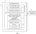
- Electronic device 10 of FIG. 1 may be a computing device such as a laptop computer, a desktop computer, a computer monitor containing an embedded computer, a tablet computer, a cellular telephone, a media player, or other handheld or portable electronic device, a smaller device such as a wristwatch device, a pendant device, a headphone or earpiece device such as an earbud, a set of earbuds, or a set of earbuds with a corresponding case that houses the earbuds, a device embedded in eyeglasses or other equipment worn on a user's head, or other wearable or miniature device, a television, a computer display that does not contain an embedded computer, a gaming device, a navigation device, an embedded system such as a system in which electronic equipment with a display is mounted in a kiosk or automobile, a wireless internet-connected voice-controlled speaker, a home entertainment device, a remote control device, a gaming controller, a peripheral user input device, a wireless base station or access point, equipment that implements the functionality
- device 10 may include components located on or within an electronic device housing such as housing 12.
- Housing 12 which may sometimes be referred to as a case, may be formed of plastic, glass, ceramics, fiber composites, metal (e.g., stainless steel, aluminum, metal alloys, etc.), other suitable materials, or a combination of these materials.
- parts or all of housing 12 may be formed from dielectric or other low-conductivity material (e.g., glass, ceramic, plastic, sapphire, etc.).
- housing 12 or at least some of the structures that make up housing 12 may be formed from metal elements.
- Control circuitry 14 may include storage such as storage circuitry 16.
- Storage circuitry 16 may include hard disk drive storage, nonvolatile memory (e.g., flash memory or other electrically-programmable-read-only memory configured to form a solid-state drive), volatile memory (e.g., static or dynamic random-access-memory), etc.
- Storage circuitry 16 may include storage that is integrated within device 10 and/or removable storage media.
- Control circuitry 14 may include processing circuitry such as processing circuitry 18. Processing circuitry 18 may be used to control the operation of device 10. Processing circuitry 18 may include on one or more processors, microprocessors, microcontrollers, digital signal processors, host processors, baseband processor integrated circuits, application specific integrated circuits, central processing units (CPUs), etc. Control circuitry 14 may be configured to perform operations in device 10 using hardware (e.g., dedicated hardware or circuitry), firmware, and/or software. Software code for performing operations in device 10 may be stored on storage circuitry 16 (e.g., storage circuitry 16 may include non-transitory (tangible) computer readable storage media that stores the software code). The software code may sometimes be referred to as program instructions, software, data, instructions, or code. Software code stored on storage circuitry 16 may be executed by processing circuitry 18.
- processing circuitry 18 may include on one or more processors, microprocessors, microcontrollers, digital signal processors, host processors, baseband processor integrated circuits, application specific integrated circuits, central processing units
- Control circuitry 14 may be used to run software on device 10 such as satellite navigation applications, internet browsing applications, voice-over-internet-protocol (VOIP) telephone call applications, email applications, media playback applications, operating system functions, etc. To support interactions with external equipment, control circuitry 14 may be used in implementing communications protocols.
- VOIP voice-over-internet-protocol
- Communications protocols that may be implemented using control circuitry 14 include internet protocols, wireless local area network (WLAN) protocols (e.g., IEEE 802.11 protocols - sometimes referred to as Wi-Fi ® ), protocols for other short-range wireless communications links such as the Bluetooth ® protocol or other wireless personal area network (WPAN) protocols, IEEE 802.1 1ad protocols (e.g., ultra-wideband protocols), cellular telephone protocols (e.g., 3G protocols, 4G (LTE) protocols, 3GPP Fifth Generation (5G) New Radio (NR) protocols, etc.), antenna diversity protocols, satellite navigation system protocols (e.g., global positioning system (GPS) protocols, global navigation satellite system (GLONASS) protocols, etc.), antenna-based spatial ranging protocols (e.g., radio detection and ranging (RADAR) protocols or other desired range detection protocols for signals conveyed at millimeter and centimeter wave frequencies), or any other desired communications protocols.
- Each communications protocol may be associated with a corresponding radio access technology (RAT) that specifies the physical connection methodology used
- Device 10 may include input-output circuitry 20.
- Input-output circuitry 20 may include input-output devices 22.
- Input-output devices 22 may be used to allow data to be supplied to device 10 and to allow data to be provided from device 10 to external devices.
- Input-output devices 22 may include user interface devices, data port devices, and other input-output components.
- input-output devices 22 may include touch sensors, displays (e.g., touch-sensitive and/or force-sensitive displays), light-emitting components such as displays without touch sensor capabilities, buttons (mechanical, capacitive, optical, etc.), scrolling wheels, touch pads, key pads, keyboards, microphones, cameras, buttons, speakers, status indicators, audio jacks and other audio port components, digital data port devices, motion sensors (accelerometers, gyroscopes, and/or compasses that detect motion), capacitance sensors, proximity sensors, magnetic sensors, force sensors (e.g., force sensors coupled to a display to detect pressure applied to the display), temperature sensors, etc.
- touch sensors e.g., touch-sensitive and/or force-sensitive displays
- light-emitting components such as displays without touch sensor capabilities, buttons (mechanical, capacitive, optical, etc.), scrolling wheels, touch pads, key pads, keyboards, microphones, cameras, buttons, speakers, status indicators, audio jacks and other audio port components
- digital data port devices motion sensors (
- keyboards, headphones, displays, pointing devices such as trackpads, mice, and joysticks, and other input-output devices may be coupled to device 10 using wired or wireless connections (e.g., some of input-output devices 22 may be peripherals that are coupled to a main processing unit or other portion of device 10 via a wired or wireless link).
- Input-output circuitry 20 may include wireless circuitry 24 to support wireless communications and/or radio-based spatial ranging operations.
- Wireless circuitry 24 may include one or more antennas 30.
- Wireless circuitry 24 may also include one or more radios 26.
- Each radio 26 may include circuitry that operates on signals at baseband frequencies (e.g., baseband processor circuitry), signal generator circuitry, modulation/demodulation circuitry (e.g., one or more modems), radio-frequency transceiver circuitry (e.g., radio-frequency transmitter circuitry, radio-frequency receiver circuitry, mixer circuitry for downconverting radio-frequency signals to baseband frequencies or intermediate frequencies between radio and baseband frequencies and/or for upconverting signals at baseband or intermediate frequencies to radio-frequencies, etc.), amplifier circuitry (e.g., one or more power amplifiers and/or one or more low-noise amplifiers (LNAs)), analog-to-digital converter (ADC) circuitry, digital-to-analog converter (DAC) circuitry, control
- each radio 26 may be mounted onto a respective substrate or integrated into a respective integrated circuit, chip, package (e.g., system-in-package), or system-on-chip (SOC). If desired, the components of multiple radios 26 may share a single substrate, integrated circuit, chip, package, or SOC.
- antenna(s) 30 may be formed using any desired antenna structures.
- antenna(s) 30 may include antennas with resonating elements that are formed from loop antenna structures, patch antenna structures, inverted-F antenna structures, slot antenna structures, planar inverted-F antenna structures, helical antenna structures, monopole antennas, dipoles, hybrids of these designs, etc.
- Filter circuitry, switching circuitry, impedance matching circuitry, and/or other antenna tuning components may be adjusted to adjust the frequency response and wireless performance of antenna(s) 30 over time.
- Transceiver circuitry in radios 26 may convey radio-frequency signals using one or more antennas 30 (e.g., antenna(s) 30 may convey the radio-frequency signals for the transceiver circuitry).
- the term "convey radio-frequency signals" as used herein means the transmission and/or reception of the radio-frequency signals (e.g., for performing unidirectional and/or bidirectional wireless communications with external wireless communications equipment).
- Antenna(s) 30 may transmit the radio-frequency signals by radiating the radio-frequency signals into free space (or to free space through intervening device structures such as a dielectric cover layer).
- Antenna(s) 30 may additionally or alternatively receive the radio-frequency signals from free space (e.g., through intervening devices structures such as a dielectric cover layer).
- the transmission and reception of radio-frequency signals by antenna(s) 30 each involve the excitation or resonance of antenna currents on an antenna resonating element in the antenna by the radio-frequency signals within the frequency band(s) of operation of the antenna.
- Radios 26 may use antenna(s) 30 to transmit and/or receive radio-frequency signals within different frequency bands at radio frequencies (sometimes referred to herein as communications bands or simply as a "bands").
- the frequency bands handled by radios 28 may include wireless local area network (WLAN) frequency bands (e.g., Wi-Fi ® (IEEE 802.11) or other WLAN communications bands) such as a 2.4 GHz WLAN band (e.g., from 2400 to 2480 MHz), a 5 GHz WLAN band (e.g., from 5180 to 5825 MHz), a Wi-Fi ® 6E band (e.g., from 5925-7125 MHz), and/or other Wi-Fi ® bands (e.g., from 1875-5160 MHz), wireless personal area network (WPAN) frequency bands such as the 2.4 GHz Bluetooth ® band or other WPAN communications bands, cellular telephone frequency bands (e.g., bands from about 600 MHz to about 5 GHz, 3G bands, 4G LTE bands, 5G New
- Each radio 26 may transmit and/or receive radio-frequency signals according to a respective radio access technology (RAT) that determines the physical connection methodology for the components in the corresponding radio.
- RAT radio access technology
- the radios 26 in device 10 may include a UWB radio for conveying UWB signals using one or more antennas 30, a Bluetooth (BT) radio for conveying BT signals using one or more antennas 30, a Wi-Fi radio for conveying WLAN signals using one or more antennas 30, a cellular radio for conveying cellular telephone signals using one or more antennas 30 (e.g., in 4G frequency bands, 5G FR1 bands, and/or 5G FR2 bands), an NFC radio for conveying NFC signals using one or more antennas 30, and a wireless charging radio for receiving wireless charging signals using one or more antennas 30 for charging a battery on device 10.
- radios 26 may include any desired combination of radios for covering any desired combination of RATs.
- Radios 26 may use antenna(s) 30 to transmit and/or receive radio-frequency signals to convey wireless communications data between device 10 and external wireless communications equipment such as one or more electronic devices 10' (e.g., one or more other devices such as device 10, a wireless access point or base station, etc.) via communications link(s) 32.
- Wireless communications data may be conveyed by radios 26 bidirectionally or unidirectionally.
- the wireless communications data may, for example, include data that has been encoded into corresponding data packets such as wireless data associated with a telephone call, streaming media content, internet browsing, wireless data associated with software applications running on device 10, email messages, etc.
- Radios 26 may also use antenna(s) 30 to perform spatial ranging operations (e.g., for identifying a distance between device 10 and an external object).
- Radios 26 that perform spatial ranging operations may include radar circuitry if desired (e.g., frequency modulated continuous wave (FMCW) radar circuitry, OFDM radar circuitry, FSCW radar circuitry, a phase coded radar circuitry, other types of radar circuitry).
- FMCW frequency modulated continuous wave
- OFDM OFDM
- FSCW radar circuitry a phase coded radar circuitry, other types of radar circuitry.
- one or more devices 10' may include a primary device (e.g., a laptop computer, a desktop computer, a tablet computer, a cellular telephone, etc.) for which device 10 is an accessory.
- a primary device e.g., a laptop computer, a desktop computer, a tablet computer, a cellular telephone, etc.
- device 10 may perform wireless communications with device 10' which may be an earbud for the other one of the user's ears.
- devices 10 and 10' may include any number of electronic devices that communicate with one another wirelessly.
- wireless circuitry 24 may include processing circuitry (e.g., one or more processors) that forms a part of processing circuitry 18 and/or storage circuitry that forms a part of storage circuitry 16 of control circuitry 14 (e.g., portions of control circuitry 14 may be implemented on wireless circuitry 24).
- Wireless circuitry 24 may include any desired number of antennas 30. Some or all of the antennas 30 in wireless circuitry 24 may be arranged into one or more phased antenna arrays (e.g., for conveying radio-frequency signals over a steerable signal beam). If desired, antenna(s) 30 may be operated using a multiple-input and multiple-output (MIMO) scheme and/or using a carrier aggregation (CA) scheme.
- MIMO multiple-input and multiple-output
- CA carrier aggregation
- FIG. 2 is a functional block diagram of wireless circuitry 24 of FIG. 1 .
- each radio 26 may be (communicably) coupled to one or more antennas 30 over one or more radio-frequency transmission lines 36.
- each radio-frequency transmission line 36 may include a ground conductor such as ground conductor 38 and a signal conductor such as signal conductor 40.
- a corresponding antenna 30 may include an antenna feed such as antenna feed 46 having ground antenna feed terminal 42 coupled to ground conductor 38 and positive antenna feed terminal 44 coupled to signal conductor 40.
- Radio-frequency transmission lines 36 may be shared between radios 26 and/or antennas 30 if desired.
- Radio-frequency front end (RFFE) modules may be interposed on one or more radio-frequency transmission lines 36.
- the radio-frequency front end modules may include substrates, integrated circuits, chips, or packages that are separate from radios 26 and may include filter circuitry, switching circuitry, amplifier circuitry, impedance matching circuitry, radio-frequency coupler circuitry, and/or any other desired radio-frequency circuitry for operating on the radio-frequency signals conveyed over radio-frequency transmission lines 36.
- Radio-frequency transmission lines are often implemented using co-axial cables.
- wireless systems having radio-frequency transmission lines implemented in this manner must employ a large number of co-axial cables and corresponding connector structures, which can be large and bulky.
- Such a configuration is especially undesirable for small form-factor devices, which have limited interior space.
- other transmission lines structures may be used instead, their use similarly faces space constraints in these small form-factor devices and can lead to degradation in wireless performance if employed in a compact wireless system. It may therefore be desirable to provide radio-frequency transmission lines in a compact manner (e.g., for small form-factor devices or other devices) while providing satisfactory wireless performance in a wireless system.
- wireless circuitry 24 may include one or more radio-frequency transmission lines 36 that are implemented from radio-frequency transmission line structures (e.g., signal traces, ground traces, etc.) spanning across one or more substrates 50 (e.g., one or more printed circuit substrates).
- radio-frequency transmission line structures e.g., signal traces, ground traces, etc.
- substrates 50 e.g., one or more printed circuit substrates.
- electronic devices e.g., device 10
- other device components e.g., storage circuitry 16, processing circuitry 18, radios 26, etc.
- radio-frequency transmission line structures e.g., forming a single radio-frequency transmission line
- the single printed circuit may require certain dimensions (e.g., a certain minimum thickness or size) and/or other specialized properties to configure the corresponding radio-frequency transmission line to exhibit a desired or satisfactory impedance at a frequency of operation.
- this desired or satisfactory impedance refers to a transmission line impedance matched with (e.g., the same as, within 0.01% of, within 0.1% of, within 1% of, within 2% of, within 5% of, etc.) the corresponding antenna impedance.
- Relying on such a specialized printed circuit may be undesirably limiting in terms of useable device space, device costs, etc., especially for a small form-factor device.
- Wireless circuitry 24 can therefore include one or more radio-frequency transmission lines 36 each formed from structures on multiple substrates 50 in device 10.
- radio-frequency transmission line 36 By forming radio-frequency transmission line 36 using transmission line structures on multiple such structures (e.g., on printed circuits substrates and/or on other substrates), device 10 can forgo the need for a bulky and/or specialized printed circuit (substrate), the inclusion of which can lead to an increased device size and/or increased costs.
- Configurations in which one or more radio-frequency transmission lines 36 are each formed from structures across multiple substrates 50 are described herein as illustrative examples.
- One or more substrates 50 onto which transmission line structures are integrated may include one or more substrates for rigid printed circuit boards and/or flexible printed circuits.
- a flexible printed circuit can include a flexible printed circuit substrate formed from polyimide, liquid crystal polymer, other flexible polymer materials, or other suitable materials.
- the flexible printed circuit may include multilayer laminated structures (e.g., layers of a conductive material such as copper and a dielectric material such as a resin that are laminated together without intervening adhesive).
- the multilayer laminated structures may, if desired, be folded or bent in multiple dimensions (e.g., two or three dimensions) and may maintain a bent or folded shape after bending (e.g., the multilayer laminated structures may be folded into a particular three-dimensional shape to route around other device components and may be rigid enough to hold its shape after folding without being held in place by stiffeners or other structures).
- a rigid printed circuit board may include a (rigid) printed circuit substrate formed from rigid printed circuit board material such as fiberglass-filled epoxy or fiberglass-epoxy laminate, ceramics, other rigid polymer materials, or other suitable materials. If desired, a printed circuit substrate may be formed from one or more of these flexible and/or rigid materials (e.g., at different portions of the substrate).
- One or more substrates 50 onto which transmission line structures are integrated may include one or more substrates for any suitable system.
- these substrates may include a package substrate such as a substrate to which one or more components and/or integrated circuit (IC) dies for a packaged system are mounted (e.g., implementing a system-in-package (SiP)), an interposer substrate such as a substrate in which conductive routing structures are formed to route signals between two or more of IC dies, packaged systems, printed circuits, etc. (e.g., implementing an interposer), or any other substrate.
- a SiP and an illustrative interposer may both include conductive (routing) traces, vias, and other structures, a SiP or an interposer may sometimes be referred to herein as a printed circuit.
- FIG. 3 is a cross-sectional view of wireless circuitry 24 having illustrative transmission line structures integrated onto multiple substrates (e.g., formed from structures across multiple substrates).
- substrates 52, 54, 56, and 58 are shown.
- Each of substrates 52, 54, 56, and 58 may be a substrate of any suitable type as described above (e.g., a rigid printed circuit board substrate, a flexible printed circuit substrate, a hybrid rigid-flexible printed circuit substrate, an interposer substrate, a package or SiP substrate, etc.).
- Substrate 52 is coupled to (e.g., mounted to or stacked on) substrate 56 through intervening or interposing substrate 54.
- Substrate 56 is coupled to (e.g., mounted to or stacked on) substrate 58.
- Conductive structures such as conductive traces, conductive vias, metal traces, metal layers, metal vias, interconnect layers, routing layers, etc., may be disposed on (e.g., embedded within, disposed on one or more external surfaces of, or disposed in other manners on one or more portions of) each of substrates 52, 54, 56, and 58 to form conductive paths that convey signals within each substrate and between different substrates.
- Transmission line structures (e.g., one or more signal traces, one or more ground traces, etc.) communicably coupling radio 26 to antenna 40 may be formed from these conductive traces, conductive vias, or other conductive structures on each of substrates 52, 54, 56, and 58.
- radio 26 is coupled (e.g., with or without other intervening interconnect structures) to conductive traces on substrate 52 such as conductive trace 62.
- Conductive trace 62 forms a first portion of a radio-frequency transmission line (e.g., radio-frequency transmission line 36 in FIG. 2 ).
- One or more conductive vias on substrate 52 such as conductive via 63 electrically connects conductive trace 62 to corresponding external contacts on substrate 52 such as contact pad 71 (e.g., implemented as a bond pad, a solder pad, etc.).
- Contact pad 71 electrically connects to conductive structures on substrates 56 and 58 (forming another portion of transmission line structures) via conductive structures on interposing substrate 54 (forming yet another portion of transmission line structures).
- substrate 54 may be omitted (e.g., contact pads on substrates 52 and 56 may be directedly connected to each other using conductive interconnect material such as solder, conductive bumps, conductive adhesive, etc., without intervening conductive structures on a separate interposing substrate).
- conductive structures on substrate 54 such as conductive routing structure 64 (e.g., implemented based on one or more conductive vertical vias, one or more conductive horizontal routing layers, and/or other conductive structures) routes an external connection on a first side of substrate 54 to another external connection on a second side of substrate 54 opposing the first side.
- Contact pad 71 on substrate 52 is connected to a corresponding contact pad 73 on the first side (e.g., a first surface) of substrate 54 via a conductive interconnect structure 72 such as solder, a conductive bump or pillar, conductive adhesive, etc.
- Contact pad 77 on substrate 56 is connected to a corresponding contact pad 75 on the second side (e.g., a second surface) of substrate 54 via a conductive interconnect structure 74 such as solder, a conductive bump or pillar, conductive adhesive, etc.
- a conductive interconnect structure 74 such as solder, a conductive bump or pillar, conductive adhesive, etc.
- conductive traces on substrate 56 such as conductive trace 66 form a second portion of the radio-frequency transmission line (e.g., radio-frequency transmission line 36 in FIG. 2 ).
- One or more conductive vias on substrate 56 such as conductive vias 65 and 67 electrically connect conductive trace 66 to corresponding external contacts on substrate 56 such as contact pad 77 for via 65 and contact pad 79 for via 67 on opposing sides of substrate 56.
- contact pad 79 electrically connects to conductive structures on substrate 58 using a conductive interconnect structure 76 such as solder, a conductive bump or pillar, conductive adhesive, etc.
- a conductive interconnect structure 76 such as solder, a conductive bump or pillar, conductive adhesive, etc.
- One or more conductive vias on substrate 58 such as conductive via 69 electrically connects conductive traces on substrate 58 such as conductive trace 68 to corresponding external contacts on substrate 58 such as contact pad 81.
- Conductive trace 68 on substrate 58 form a third portion of the radio-frequency transmission line (e.g., radio-frequency transmission line 36 in FIG. 2 ).
- Conductive trace 68 at least partly forming the radio-frequency transmission line portion on substrate 58 is coupled (e.g., with or without other intervening interconnect structures) to antenna 30.
- antenna 30 may be electrically connected to conductive trace 66 on substrate 56 without intervening conductive structures on substrate 58
- radio 26 may be electrically connected to conductive trace 66 on substrate 56 without intervening conductive structures on interposer 54 and on substrate 52, etc.
- any suitable number of conductive traces and vias may be implemented on each substrate to form the appropriate transmission line structures for a radio-frequency transmission line and any additional radio-frequency transmission lines formed across multiple substrates in a similar manner, if desired.
- one or more conductive traces and vias in each substrate may be associated with a signal path or conductor (e.g., signal conductor 40 in FIG. 2 ), one or more conductive traces and vias in each substrate may be associated a ground path or conductor (e.g., ground conductor 38 in FIG. 2 ), etc. Additional signal and ground conductors (e.g., for the same radio-frequency transmission line or additional radio-frequency transmission lines) may be formed in a similar manner if desired.
- one or more radio-frequency transmission lines can each be formed from conductive structures on each of the substrates (e.g., conductive layers, conductive vias, contact pads, etc.), from conductive structures between or external to corresponding substrates (e.g., conductive interconnection structures such as solder, bumps, etc.), from non-conductive structures on each of the substrates (e.g., substrate layers and dielectric layers that provide the appropriate isolation and/or separation between corresponding conductive structures), from non-conductive structures between or external to corresponding substrates (e.g., spacer structures or other structures that provide the appropriate isolation and/or separation between corresponding substrates).
- conductive structures on each of the substrates e.g., conductive layers, conductive vias, contact pads, etc.
- conductive interconnection structures such as solder, bumps, etc.
- non-conductive structures on each of the substrates e.g., substrate layers and dielectric layers that provide the appropriate isolation and/or separation between corresponding conductive structures
- transmission line structures for a radio-frequency transmission line are integrated onto substrates that serve other functions in device 10 (e.g., printed circuit substrates that already serve other functions in the device such as a main printed circuit board substrate that provides structural support and signal routing for one or more components in the device, a printed circuit substrate on which storage and processing circuitry and/or other circuitry is mounted, a printed circuit substrate on which an antenna is disposed, a substrate that providing routing between components on one printed circuit and components on another printed circuit, a substrate that serves other suitable functions, a substrate that serves a combination of these functions, etc.), compact transmission line structures having an impedance matched to the corresponding antenna impedance can be implemented in the device without requiring a large footprint in the device (e.g., compared to a co-axial cable connector used to support a co-axial cable).
- Configurations in which a transmission line impedance matches that of the coupled antenna are described herein an illustrative example. If desired, other characteristics of the transmission line can also be tuned to effectively convey signals between the radio and the antenna. If desired, to match the transmission line impedance to the antenna impedance, the transmission line impedance need not be exactly the same as the antenna impedance as there may be some mismatch tolerance. If desired, this mismatch could be resolved using additional impedance matching components or structures. Configurations in which the radio-frequency transmission line is coupled to the antenna without these additional intervening impedance matching components or structures are described herein as an illustrative example.
- substrate 52 may be a package substrate for a system-in-package (SiP)
- substrate 56 may be a flexible printed circuit substrate for a main system printed circuit which provides structural support and signal routing to and from different functional components or subsystems in device 10
- substrate 58 may be a flexible printed circuit substrate for a flexible printed circuit that provides routing to one or more antennas.
- the one or more antennas coupled to the flexible printed circuit associated with substrate 58 may be disposed on an antenna carrier (e.g., a laser direct structuring (LDS) plastic on which the one or more antennas are patterned) mounted to substrate 58.
- LDS laser direct structuring
- One or more antennas implemented in other manners may also be used, if desired.
- substrate 54 may be an interposer substrate for an interposer that interfaces between the SiP and the main system printed circuit (e.g., provides signal routing between one or more components on the SiP and one or more components on the main system printed circuit.
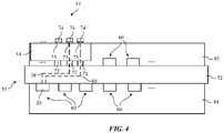
- FIG. 4 is a cross-sectional view of an illustrative interposer 55 (e.g., associated with substrate 54 of FIG. 3 ) mounted to an illustrative SiP 53 (e.g., associated with substrate 52 of FIG. 3 ).
- SiP 53 includes a package substrate 52 (sometimes referred to as carrier substrate 52) to which components 80 are mounted (e.g., on both sides of package substrate 52 using solder, wire bonds, conductive bumps, or other conductive interconnect structures).
- components 80 may include one or more integrated circuit dies (e.g., each implementing one or more of storage circuitry 16, processing circuitry 18, radio(s) 26, signal processing circuitry and driver circuitry for one or more input-output devices, power management circuitry, clock management circuitry, etc.), other active components (e.g., input-output devices 22, programmable devices, diodes, other semiconductor devices, etc.), passive components (e.g., resistors, capacitors, inductors, etc.), electromechanical components, and any other suitable discrete devices.
- integrated circuit dies e.g., each implementing one or more of storage circuitry 16, processing circuitry 18, radio(s) 26, signal processing circuitry and driver circuitry for one or more input-output devices, power management circuitry, clock management circuitry, etc.
- other active components e.g., input-output devices 22, programmable devices, diodes, other semiconductor devices, etc.
- passive components e.g., resistors, capacitors, inductors, etc.
- a particular component 80 implements radio 26 covering one or more RATs (e.g., an integrated circuit die that includes one or more radios).
- a radio-frequency transmission line such as radio-frequency transmission line 36, and if desired, one or more additional radio-frequency transmission lines, may couple radio 26 mounted to substrate 52 to one or more antennas.
- conductive structures on package substrate 52, conductive structures on substrate 54, and conductive structures between substrates 52 and 54 form radio-frequency transmission line 36 coupled to radio 26.
- signal conductor 38 may be implemented using a first set of conductive structures across substrates 52 and 54, and substrates 56 and 58 in FIG.
- ground conductor 40 may be implemented using a second set of conductive structures across substrates 52 and 54, and substrates 56 and 58 in FIG. 3 . If desired, one or more additional signal conductors may share some of the conductive structures in the first set and one or more additional ground conductors may share some of the conductive structures in the second set.
- one or more radio-frequency transmission lines 36 are implement using structures associated with SiP 53 and interposer 55 such as flexible printed circuits such as those implemented by substrates 56 and 58 in FIG. 3 instead of a co-axial cable, one or more co-axial cable connectors can be omitted.
- the omission of the bulky co-axial cable connectors not only provides interior space savings, but also allows the SiP to be fully encapsulated (e.g., compared to scenarios in which exposed co-axial cable connectors are needed to provide the co-axial cable connection, leading to one side of the SiP unable to be encapsulated thereby causing components on that side to be susceptible to unwanted weathering).
- encapsulation 82 and 84 components 80 on both sides of substrate 52 and connections between SiP 53 and interposer 54 are covered by encapsulation 82 and 84.
- electromagnetic shielding layers may be deposited on encapsulation 82 and 84 that shield components on SiP 53 from undesired electromagnetic interference.
- Encapsulation 82 and 84 may be formed from any suitable number and type of encapsulant material such as plastics or specifically thermoplastics, ceramic, etc. Similarly, any suitable process (e.g., spin-on, molding, underfill, etc.) may be used to form encapsulation 82 and 84, and the shielding layers.
- interposer 55 can serve as the exclusive electrical interface through which components on SiP 53 are accessed.
- connection to components on SiP 53 may be made through external contacts on one side of substrate 54 (e.g., contact pads 75).
- one or more additional printed circuits e.g., a flexible printed circuit associated with substrate 56 of FIG. 3 ) having corresponding contact pads can electrically connect to contact pads 75 via conductive interconnect structures 74.
- each of substrates 52, 54, 56, and 58 may serves other functions (e.g., other than supporting the integration of transmission line structures) and may have corresponding structures disposed thereon to serves those functions.
- substate 52 in FIG. 4 may include additional structures (e.g., conductive routing, or interconnect layers, vias, etc.) for performing signal routing for other components 80 (e.g., other than radio 26), and similarly, substrate 54 in FIG.
- additional structures e.g., conductive routing or interconnect layers, vias, etc.
- Substrates 56 and 58 may similarly have corresponding additional structures thereon serving any suitable routing functions.
- FIG. 5 is an exploded perspective view of illustrative transmission line structures for a radio-frequency transmission line that are distributed or integrated across multiple substrates.
- transmission line structures for a radio-frequency transmission line are formed from three illustrative sets of stacked metal and substrate layers.
- the first set of metal and substrate layers 90 includes a substrate layer 100 and metal layers 101 and 102 on substrate layer 100 (e.g., where metal layer 102 is on a top surface of substrate 100 and metal layer 101 is embedded within substrate 100 or on a bottom surface of substrate 100).
- the second set of metal and substrate layers 92 includes substrate layers 110 and 118 (sometimes referred to herein, collectively, as a substrate, which can have multiple substrate layers laminated or adhered together) and a metal layer having metal traces 112, 114, and 116 between substrate layers 110 and 118 (e.g., metal traces 112, 114, and 116 embedded within a multilayer substrate).
- Metal trace 112 may be laterally separated and electrically isolated from metal trace 114 by a gap filled with non-conductive material (e.g., a portion of the multilayer substrate or a substrate layer, a dielectric layer, an adhesive, an insulator, etc.).
- metal traces 116 may be laterally separated and electrically isolated from metal trace 114 by a gap filed with non-conductive material.
- the third set of metal and substrate layers 94 includes substrate layers 120 and 124 (sometimes referred to herein, collectively as a substrate, which can have multiple substrate layers laminated or adhered together), metal layer 122 between substrate layers 120 and 124 (e.g., embedded within a multilayer substrate), and metal layer 126 on substrate layer 124 (e.g., on a top surface of the multilayer substrate).
- substrate layers 120 and 124 sometimes referred to herein, collectively as a substrate, which can have multiple substrate layers laminated or adhered together
- metal layer 122 between substrate layers 120 and 124 e.g., embedded within a multilayer substrate
- metal layer 126 on substrate layer 124 e.g., on a top surface of the multilayer substrate.
- non-conductive material e.g., a portion of the multilayer substrate or a substrate layer, a dielectric layer, an adhesive, etc.
- one or more substrate layers may sometimes be referred to herein as insulators or insulator layers (e.g., that separate and provide insulation between ground traces and signal traces, between different ground traces, between different signal traces, etc.).
- the overall radio-frequency transmission line may inherently serve as an impedance matching structure that allows for signal conveyance to and from the antenna without mismatch loss (e.g., the radio-frequency transmission line inherently does not suffer from mismatch loss when conveying signals to and from the antenna).
- any separate intervening impedance matching structures e.g., discrete components such as capacitor, inductors, etc., external to the radio-frequency transmission line structures
- additional impedance matching is not required.
- the set of layers 94 forms a portion of a first flexible printed circuit (e.g., a flexible printed circuit having a multilayer laminated structure or substrate, a flexible printed circuit associated with substrate 58 in FIG. 3 , etc.).
- the set of layers 92 forms an overlapping portion of a second flexible printed circuit (e.g., a flexible printed circuit having a multilayer laminated structure or substrate, a flexible printed circuit associated with substrate 56 in FIG. 3 , etc.), and the set of layers 90 forms an overlapping portion of a SiP or a SiP substrate (e.g., a SiP associated with substrate 52 in FIG. 3 , a package substrate 52 for SiP 53 in FIG. 4 , etc.).
- Portions of the SiP or the SiP substrate are omitted from the set of layers 90 shown in FIG. 5 for the sake of clarity.
- Conductive structures e.g., metal layers, metal traces, etc.
- Conductive structures e.g., metal layers, metal traces, etc.
- layers 90, 92, and 94 are connected to each other to collectively form transmission line structures for a radio-frequency transmission line.
- a radio-frequency transmission line may exhibit a particular satisfactory characteristic impedance (e.g., a 50-Ohm impedance transmission line) to minimize antenna signal losses (e.g., signal reflection) between the antenna and the radio-frequency transmission line.
- the characteristic impedance of the transmission line may be satisfactory at least in part because it is matched to (e.g., the same as, within 0.01% of, within 0.1% of, within 1% of, within 2% of, within 5% of, etc.) the corresponding impedance of the antenna to which it is coupled such that mismatch loss is minimized.
- mismatch loss is minimized.
- conductive structures from multiple printed circuits and other structures may be selectively configured and connected to tune the composite or collective characteristic impedance of the radio-frequency transmission line.
- the relative configuration of layers within the sets 90, 92, and 94 (and other neighboring or adjacent structures) may, collectively, contribute to the composite or collective impedance of the overall radio-frequency transmission line.
- the individual characteristic impedance of a first radio-frequency transmission line portion implemented on set of layers 90, the individual characteristic impedance of a second radio-frequency transmission line portion implemented on set of layers 92, the individual characteristic impedance of a third radio-frequency transmission line portion implemented on set of layers 94 may, taken individually (e.g., taken each in isolation), exhibit respective individual impedances that are more capacitive (e.g., less than a target 50-Ohm impedance line) or more inductive (e.g., greater than a target 50-Ohm impedance line) than the target characteristic impedance of the radio-frequency transmission line (e.g., a 50-Ohm impedance transmission line).
- the three radio-frequency transmission line portions along with any corresponding interconnect and neighboring structures will form a radio-frequency transmission line with the target characteristic impedance (e.g., a 50-Ohm impedance transmission line).
- the transmission line structures across multiple substrates as described in connection with FIGS. 3 and 4 may also collectively exhibit a target overall characteristic impedance (sometimes referred to herein as a collective or composite impedance) even though the transmission line structures individually do not exhibit the target impedance.
- the radio-frequency transmission line configured in this manner can convey radio-frequency signals to and from the antenna without mismatch loss.
- discrete components such as inductors and capacitors useable for impedance matching (e.g., impedance matching structures external to the printed circuit structures forming the radio-frequency transmission line) can therefore be omitted as the radio-frequency transmission line itself serves inherently as an impedance matching structure.
- the impedance offsets of the different portion of the radio-frequency transmission line from the target impedance are not matched using the discrete components.
- the different portions of the radio-frequency transmission line on the different printed circuits are configured or tuned relative to each other (e.g., by adjust layer thickness, distance between layers, layer geometry, layer material, etc.) to directly achieve signal conveyance without mismatch loss.
- a radio-frequency transmission line exhibits an impedance of 50 Ohms
- the impedance of the radio-frequency transmission line is frequency-dependent (e.g., dependent on the one or more frequencies of radio-frequency signals conveyed by the radio-frequency transmission line between the antenna and the radio).
- the radio-frequency transmission line may be configured to exhibit any suitable target input, output, and/or characteristic impedance such as an impedance of 50 Ohms, an impedance between 45-55 Ohms, an impedance between 40-60 Ohms, etc.
- each of the separate radio-frequency transmission line portions may exhibit an individual impedance that is more capacitive (e.g., less than) or more inductive (e.g., greater than) than the impedance of the overall radio-frequency transmission line.
- the individual impedances along each radio-frequency transmission line portion may exhibit an input, output, and/or characteristic impedance within 1%, within 2%, within 5%, within 10%, within 20%, etc. of the impedance of the overall radio-frequency transmission line at the one or more frequencies of operation.
- different metal layers may be selectively interconnected with each other at corresponding contact locations (e.g., using vias and routing layers within substrate layers, using contact or solder pads at the surface of the substrate layers, using solder blocks, other solder structures, or other conductive interconnect structures between substrate layers of different or the same set of layers each set associated with a printed circuit, package, interposer, etc.). Additionally, distances or separation between the different printed circuits, packages, interposers, etc.
- an individual (characteristic) impedance of a transmission line portion on a single printed circuit may be defined by the separation of signal and ground conductors by insulator structures within that single printed circuit as well as by the dimension and geometry of the signal and ground conductors, the properties of the insulator structures, and other characteristics of that single printed circuit.
- the characteristics of single printed circuit may be too restrictive in providing the desired impedance of the overall transmission line (e.g., solely based on the transmission line portion on the single printed circuit).
- the characteristics of the transmission line portion on the single printed circuit may be adjusted or supplemented by these neighboring elements to collectively achieve the desired impedance of the overall transmission line.
- one or more interconnect structures may connect metal layer or trace 101 to metal trace 114 across illustrative contact location 130-1 and 130-2.
- One or more interconnect structures may connect metal trace 114 to metal layer or trace 126 across illustrative contact locations 144-1 and 144-1.
- Metal traces 101, 114, and 126, as interconnected, may form a signal conductor (e.g., signal conductor 40 in FIG.
- metal trace 101 may be coupled to a radio such as radio 26 in FIG. 2
- metal trace 126 may be coupled to an antenna such as antenna 30 at positive antenna feed terminal 44 in FIG. 2 .
- One or more interconnect structures may connect metal layer or trace 102 to metal trace 116 across illustrative contact locations 132-1 and 132-2.
- One or more interconnect structures may connect metal layer or trace 102 to metal trace 112 across illustrative contact locations 134-1 and 134-2.
- One or more interconnect structures may connect metal trace 112 to metal layer or trace 122 across one or more illustrative contact locations (e.g., across an illustrative set of three locations 140-1 and 140-2).
- One or more interconnect structures may connect metal trace 116 to metal layer or trace 122 across one or more illustrative contact locations (e.g., across an illustrative set of three locations 142-1 and 142-2).
- Metal traces 102, 112, 116, and 122 may form one or more ground conductor portions (e.g., ground conductor 38 in FIG. 2 ) for the radio-frequency transmission line.
- ground conductor metal trace 102 On one end of the ground conductor metal trace 102 may be coupled to a radio such as radio 26 and other device structures (e.g., a battery, other grounding structures for device components, a device housing, etc.), and on the other of the ground conductor, metal trace 122 may be coupled to an antenna such as antenna 30 at ground antenna feed terminal 42 in FIG. 2 .
- FIG. 6 is an illustrative side view of sets of layers 90, 92, and 94 of FIG. 5 when assembled (e.g., interconnected with each other, mounted to each other, etc.). Configurations in which each set of sets 90, 92, and 94 forms a different printed circuit having a separate substrate are described as illustrative examples (e.g., referred to herein sometimes as printed circuit 90, printed circuit 92, and printed circuit 94).
- interconnect structures 131 electrically connect metal trace 101 to a metal trace in metal layer 115 (e.g., to metal trace 114 in FIG. 5 that may be formed in the same metal layer 115 as metal traces 112 and 116).
- Interconnect structures 131 electrically connect metal trace 102 to a metal trace in metal layer 115 (e.g., to metal trace 112 in FIG. 5 that may be formed in the same metal layer 115 as metal traces 114 and 116).
- Similar additional interconnect structures may also electrically connect metal trace 102 to metal trace 116 in FIG. 5 (in layer 115 in FIG. 6 ).
- Interconnect structures 131 and 133 and the additional interconnect structures may include conductive printed circuit routing structures such as vias, interconnect layers, external contact pads etc., on printed circuit 90 and on printed circuit 92, and may include conductive structures between printed circuit 90 and printed circuit 92 such as solder (balls, bumps, blocks, etc.) or other conductive material that connects corresponding contact pads on printed circuits 90 and 92.
- conductive printed circuit routing structures such as vias, interconnect layers, external contact pads etc., on printed circuit 90 and on printed circuit 92
- conductive structures between printed circuit 90 and printed circuit 92 such as solder (balls, bumps, blocks, etc.) or other conductive material that connects corresponding contact pads on printed circuits 90 and 92.
- Interconnect structures 141 electrically connect a metal trace in metal layer 115 (e.g., metal trace 112 in FIG. 5 ) to metal trace 122. Similar additional interconnect structures may also electrically connect metal trace 116 in FIG. 5 or in layer 115 in FIG. 6 to metal trace 122. Interconnect structures 143 electrically connect a metal trace in metal layer 115 (e.g., metal trace 114 in FIG. 5 ) to metal trace 126.
- Interconnect structures 141 and 143 and the additional interconnect structures may include conductive printed circuit routing structures such as vias, interconnect layers, external contact pads etc., on printed circuit 92 and on printed circuit 94, and may include conductive structures between printed circuit 92 and printed circuit 94 such as solder (balls, bumps, blocks, etc.) or other conductive material that connects corresponding contact pads on printed circuits 92 and 94.
- conductive printed circuit routing structures such as vias, interconnect layers, external contact pads etc., on printed circuit 92 and on printed circuit 94
- conductive structures between printed circuit 92 and printed circuit 94 such as solder (balls, bumps, blocks, etc.) or other conductive material that connects corresponding contact pads on printed circuits 92 and 94.
- interconnect structures 131 and 133 may be controlled to preserve a desired distance (e.g., distance 150 in FIG. 5 ) between printed circuits 90 and 92 (e.g., between metal traces in printed circuits 90 and 92) and to account for capacitive loading between different elements forming interconnect structures 131 and 133 (e.g., capacitive loading associated with sizes of solder pads at corresponding interfaces of printed circuits 90 and 92) in controlling the overall impedance of the radio-frequency transmission line.
- a desired distance e.g., distance 150 in FIG. 5
- capacitive loading between different elements forming interconnect structures 131 and 133 e.g., capacitive loading associated with sizes of solder pads at corresponding interfaces of printed circuits 90 and 92
- interconnect structures 141 and 143 may also be controlled to preserve a desired distance (e.g., distance 152 in FIG. 5 ) between printed circuits 92 and 94 (e.g., between metal traces in printed circuits 92 and 94) and to account for capacitive loading between different elements forming interconnect structures 141 and 143 (e.g., capacitive loading associated with sizes of solder pads at corresponding interfaces of printed circuits 92 and 94) in controlling the overall impedance of the radio-frequency transmission line.
- a desired distance e.g., distance 152 in FIG. 5
- capacitive loading between different elements forming interconnect structures 141 and 143 e.g., capacitive loading associated with sizes of solder pads at corresponding interfaces of printed circuits 92 and 94
- components or structures 154 and 156 may be disposed between printed circuits 90, 92, and 94 for controlling and/or maintaining distances between printed circuits 90, 92, and 94.
- components or structures 154 and 156 may be dedicated spacer structures, may be components disposed on one or more of printed circuits 90, 92, and 94, may be components separate from printed circuits 90, 92, and 94, etc.
- the configuration of printed circuits 90, 92, and 94 in FIG. 6 provides a manner to implement a radio-frequency transmission line across printed circuits 90, 92, and 94 to collectively exhibit a composite impedance for the radio-frequency transmission line that is matched to the corresponding antenna impedance.
- a patterned grounding scheme connecting different reference ground layers in printed circuits 90, 92, and 94 e.g., using conductive structures 133 and 141) as shown in FIG.
- conductive structures 133 and 141 may be located across any suitable overlapping portions of metal traces 102, 112 in layer 115, 116 in layer 115, and 122 at any suitable location to ensure proper grounding across all of these metal (ground) traces in different printed circuits, thereby allowing return current to move freely along different portions of the ground conductor in different printed circuits.
- transmission line structures integrated across printed circuits 90, 92, and 94 as described in connection with FIGS. 5 and 6 are merely illustrative.
- the description in connection with FIGS. 5 and 6 may similarly apply to the transmission line structures described in connection with FIGS. 2-4 (e.g., transmission line structures across printed circuits 52, 54, 56, and 58 in FIG. 3 may collectively form a radio-frequency transmission line with an impedance matched to the antenna impedance by controlling the various characteristics described in connection with printed circuits 90, 92, and 94 in FIGS. 5 and 6 ).
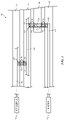
- FIG. 7 An illustrative electronic device 10, such as a wristwatch device, an earbud, an earpiece device, or any other device described in connection with FIG. 1 , having wireless circuitry employing one or more radio-frequency transmission lines each integrated across multiple printed circuits as described in connection with FIGS. 2-6 is shown in FIG. 7 .
- housing 12 of device 10 includes first portion 162 and second portion 164.
- Housing 12 may include one or more ports such as ports that are aligned with one or more internal components such as speaker 176 (e.g., a speaker port).
- Housing 12 separates an exterior of device 10 from an interior (e.g., interior 160) of device 10, in which components of device 10 are disposed.
- the components of device 10 may include battery 178, microphone 180, any other components 182 such as those described in connection with FIG. 1 .
- One or more of these components (e.g., processing circuitry 18, storage circuitry 16, radio 26, antenna 30, input-output devices 22, etc.) may be mounted on one or more printed circuits in device 10.
- device 10 may include a printed circuit to which a radio, processing circuitry, storage circuitry, etc. are mounted in a package (e.g., forming SiP 168), a printed circuit serving as a system printed circuit that extends across interior 160 of device 10 (e.g., extending across first and second portions 162 and 164) to provide structural support and connectivity across different sub-systems in device 10 (e.g., forming system flexible printed circuit 166), a printed circuit that serves as a routing interface between components mounted to SiP 168 and system flexible printed circuit 166 (e.g., forming interposer 170), and a printed circuit that provides antenna signal routing to and from one or more antennas such as antenna 30 (e.g., forming antenna flexible printed circuit 172).
- antenna 30 may be patterned (e.g., using an LDS process) on an antenna carrier 174 (e.g., an LDS plastic) mounted on flexible printed circuit 172.
- a radio in SiP 168 may be coupled to antenna 30 using a radio-frequency transmission line having transmission line structures that extend across and are integrated with SiP 168, interposer 170, system flexible printed circuit 166, and antenna flexible printed circuit 172 (e.g., using configurations as described in connection with FIGS. 2-6 ), thereby providing a compact radio-frequency transmission line exhibiting an impedance matched with an impedance of antenna 30 without the need for separate intervening impedance matching elements such as capacitor and/or inductors.
- Transmission line structures on antenna flexible printed circuit 172 may be coupled to antenna 30 on carrier 174 via one or more suitable conductive interconnect structures (e.g., solder, welds, conductive adhesive, screws, brackets, etc.) to feed antenna 30.
- radio-frequency transmission line structures include a first printed circuit having a first substrate and first conductive traces disposed on the first substrate, the first conductive traces exhibiting a first impedance; and a second printed circuit having a second substrate and second conductive traces disposed on the second substrate, the second conductive traces exhibiting a second impedance, the second printed circuit at least partially overlapping the first printed circuit and being separated from the first printed circuit by a distance, and the first impedance, the second impedance, and the distance separating the second printed circuit from the first printed circuit collectively defining a composite impedance of the radio-frequency transmission line structures.
- the composite impedance of the radio-frequency transmission line structures is different than the first impedance exhibited by the first conductive traces and different than the second impedance exhibited by the second conductive traces.
- the first conductive traces include a ground trace and a signal trace separated from the ground trace by an insulator and the ground trace, the signal trace, and the insulator at least partially define the first impedance associated with the first conductive traces.
- the second conductive traces include an additional ground trace and an additional signal trace separated from the additional ground trace by an additional insulator and the additional ground trace, the additional signal trace, and the additional insulator at least partially define the second impedance associated with the second conductive traces.
- the radio-frequency transmission line structures include a third printed circuit having a third substrate and third conductive traces on the third substrate, the third printed circuit at least partially overlapping the second printed circuit and being separated from the second printed circuit by an additional distance.
- the third conductive traces exhibit a third impedance and the third impedance and the additional distance separating the third printed circuit from the second printed circuit collectively further define the composite impedance of the radio-frequency transmission line structures.
- the first printed circuit includes a first flexible printed circuit and the second printed circuit includes a second flexible printed circuit.
- the radio-frequency transmission line structures include a component between the first printed circuit and the second printed circuit and that is configured to maintain the distance separating the second printed circuit from the first printed circuit.
- a radio-frequency transmission line includes a signal conductor that includes first signal traces on a first printed circuit and second signal traces on a second printed circuit; and a ground conductor that includes first ground traces on the first printed circuit and second ground traces on the second printed circuit, the first signal traces and the first ground traces on the first printed circuit exhibiting a first impedance, the second signal traces and the second ground traces on the second printed circuit exhibiting a second impedance, and the radio-frequency transmission line exhibiting a characteristic impedance that is different from the first impedance and that is different from the second impedance.
- the radio-frequency transmission line includes conductive interconnect structures that couple, at a plurality of locations, the first ground traces on the first printed circuit to the second ground traces on the second printed circuit.
- the radio-frequency transmission line includes additional conductive interconnect structures that couple the first signal traces on the first printed circuit to the second signal traces on the second printed circuit, the conductive interconnect structures and the additional conductive interconnect structures including solder between the first printed circuit and the second printed circuit.
- the conductive interconnect structures include solder between the first printed circuit and the second printed circuit, a first contact pad on the first printed circuit, a second contact pad on the second printed circuit, a first conductive via on the first printed circuit, and a second conductive via on the second printed circuit.
- the first conductive via couples the first ground traces to the first contact pad
- the second conductive via couples the second ground traces to the second contact pad
- the solder couples the first contact pad to the second contact pad.
- the radio-frequency transmission line is configured to convey radio-frequency signals at a frequency
- the characteristic impedance exhibited by the radio-frequency transmission line is between 40 Ohms and 60 Ohms at the frequency
- the first individual impedance is greater than or less than 50 Ohms
- the second impedance is greater than or less than 50 Ohms.
- an electronic device includes, a radio; an antenna; a first printed circuit substrate; a second printed circuit substrate that at least partially overlaps the first printed circuit substrate; and a radio-frequency transmission line that communicably couples the radio to the antenna, the radio-frequency transmission line having a first transmission line portion on the first printed circuit substrate and a second transmission line portion on the second printed circuit substrate, the first transmission line portion exhibiting a first impedance, the second transmission line portion exhibiting a second impedance, and the radio-frequency transmission line exhibiting a collective impedance that is different than the first impedance and different than the second impedance.
- the electronic device includes components adjacent to the first printed circuit substrate and the second printed circuit substrate, the components, the first transmission line portion, and the second transmission line portion collectively exhibit the collective impedance of the radio-frequency transmission line.
- the first printed circuit substrate includes a first flexible printed circuit substrate
- the first transmission line portion includes conductive traces on the first flexible printed circuit
- the second printed circuit substrate includes a second flexible printed circuit
- the second transmission line portion includes additional conductive traces on the second flexible printed circuit.
- the electronic device includes control circuitry coupled to the radio and configured to control an operation of the radio
- the first printed circuit substrate is a package substrate for a package
- the control circuitry and the radio are mounted to the package substrate
- encapsulation material is disposed on the package substate and encapsulates the control circuitry and the radio.
- the electronic device is a portable electronic device and includes a housing having a speaker port; a speaker aligned with the speaker port; a microphone; a battery; and control circuitry coupled to the radio, the speaker, the microphone, and the battery.
- the electronic device is a wireless earbud.
Landscapes
- Engineering & Computer Science (AREA)
- Microelectronics & Electronic Packaging (AREA)
- Signal Processing (AREA)
- Physics & Mathematics (AREA)
- Acoustics & Sound (AREA)
- Computer Networks & Wireless Communication (AREA)
- Transceivers (AREA)
Abstract
Description
- This application claims priority to
U.S. patent application No. 17/380,491, filed July 20, 2021 - This disclosure relates generally to electronic devices, including electronic devices with wireless circuitry.
- Electronic devices are often provided with wireless capabilities. An electronic device with wireless capabilities has wireless circuitry that includes one or more antennas and one or more radios, with corresponding radio-frequency transmission lines that convey radio-frequency signals between the antennas and the radios.
- A radio-frequency transmission line can often be implemented using a co-axial cable. However, the co-axial cable and its corresponding connector structures are bulky and consume excessive space within the electronic device. It can therefore be challenging to design compact electronic devices while still providing transmission lines with satisfactory performance.
- An electronic device may include wireless circuitry having one or more radios and one or more antennas. A radio-frequency transmission line may couple each antenna to a corresponding radio. The radio-frequency transmission line may be integrated into printed circuit structures across one or more overlapping printed circuits. If desired, these printed circuits can include flexible printed circuits, rigid printed circuit boards, interposers, package substrates, etc.
- Conductive structures in these printed circuits interconnected by solder or other conductive interconnect structures between the printed circuits may form portions of the radio-frequency transmission line. Each portion of the radio-frequency transmission line individually may exhibit an (individual) impedance that is offset from a target (composite or collective characteristic) impedance of the overall radio-frequency transmission line. By controlling the configuration (e.g., thicknesses of conductive and insulator layers) of each of the printed circuits, the configuration (e.g., distances) between the printed circuits (e.g., between conductive structures in the printed circuits), and the configuration of the printed circuits relative to other neighboring structures (e.g., structures or components adjacent to one or more of these printed circuits), the portions of the radio-frequency transmission line may collectively exhibit the target impedance for the overall radio-frequency transmission line that is properly impedance-matched for coupling the radio to the antenna and for operation at one or more corresponding frequencies of operation.
- The radio-frequency transmission line configured in this manner can convey radio-frequency signals to and from the antenna without mismatch loss. Accordingly, discrete components such as inductors and capacitors useable for impedance matching (e.g., impedance matching structures external to the printed circuit structures forming the radio-frequency transmission line) can therefore be omitted as the radio-frequency transmission line itself serves inherently as an impedance matching structure. In other words, the impedance offsets of the different portion of the radio-frequency transmission line (from the target impedance) are not matched using the discrete components. Rather, the different portions of the radio-frequency transmission line on the different printed circuits are configured or tuned relative to each other (e.g., by adjust layer thickness, distance between layers, layer geometry, layer material, etc.) to directly achieve signal conveyance without mismatch loss.
- In this manner, the electronic device can use printed circuits structures (e.g., on printed circuits that also serve other functions in the electronic device) to integrate radio-frequency transmission line structures. This omits the need for bulky radio-frequency transmission line structures (e.g., co-axial cables and their connectors) and provides a compact radio-frequency transmission line having satisfactory performance. As an illustrative example and as further detailed herein, the satisfactory performance of the radio-frequency transmission line is characterized at least by an impedance associated with the radio-frequency transmission line that is matched with the impedance of the coupled antenna.
- An aspect of the disclosure provides radio-frequency transmission line structures. The radio-frequency transmission line structures can exhibit a composite impedance and can include a first printed circuit and a second printed circuit. The first printed circuit can have a first substrate and first conductive traces on the first substrate. The first conductive traces can exhibit a first impedance. The second printed circuit can have a second substrate and second conductive traces on the second substrate. The second conductive traces can exhibit a second impedance. The second printed circuit can at least partially overlap the first printed circuit and can be separated from the first printed circuit by a distance. The first impedance, the second impedance, and the distance separating the second printed circuit from the first printed circuit can collectively define the composite impedance of the radio-frequency transmission line structures.
- An aspect of the disclosure provides a radio-frequency transmission line. The radio-frequency transmission line can include a signal conductor and a ground conductor. The signal conductor can include first signal traces on a first printed circuit and second signal traces on a second printed circuit. The ground conductor can include first ground traces on the first printed circuit and second ground traces on the second printed circuit. The first signal traces and the first ground traces on the first printed circuit can exhibit a first impedance. The second signal traces and the second ground traces on the second printed circuit can exhibit a second impedance. The radio-frequency transmission line can exhibit a characteristic impedance that is different from the first impedance and that is different from the second impedance.
- An aspect of the disclosure provides an electronic device. The electronic device can include a radio, an antenna, a first printed circuit substrate, a second printed circuit substrate that at least partially overlaps the first printed circuit substrate, and a radio-frequency transmission line that communicably couples the radio to the antenna. The radio-frequency transmission line can have a first transmission line portion on the first printed circuit substrate and a second transmission line portion on the second printed circuit substrate. The first transmission line portion can exhibit a first impedance. The second transmission line portion can exhibit a second impedance. The radio-frequency transmission line can exhibit a collective impedance that is different than the first impedance and different than the second impedance.
-
-
FIG. 1 is a block diagram of an illustrative electronic device having wireless circuitry in accordance with some embodiments. -
FIG. 2 is a block diagram of illustrative wireless circuitry having transmission line structures in accordance with some embodiments. -
FIG. 3 is a cross-sectional view of illustrative transmission line structures formed across multiple stacked substrates in accordance with some embodiments. -
FIG. 4 is a cross-sectional view of an illustrative system-in-package having wireless circuitry and transmission line structures in accordance with some embodiments. -
FIG. 5 is an exploded perspective view of illustrative substrate layers and conductive structures forming transmission line structures for a radio-frequency transmission line in accordance with some embodiments. -
FIG. 6 is an illustrative side view of assembled substrate layers and conductive structures forming transmission line structures in accordance with some embodiments. -
FIG. 7 is a diagram of an illustrative electronic device implementing transmission line structures for wireless circuitry using multiple stacked substrates in accordance with some embodiments. -
Electronic device 10 ofFIG. 1 may be a computing device such as a laptop computer, a desktop computer, a computer monitor containing an embedded computer, a tablet computer, a cellular telephone, a media player, or other handheld or portable electronic device, a smaller device such as a wristwatch device, a pendant device, a headphone or earpiece device such as an earbud, a set of earbuds, or a set of earbuds with a corresponding case that houses the earbuds, a device embedded in eyeglasses or other equipment worn on a user's head, or other wearable or miniature device, a television, a computer display that does not contain an embedded computer, a gaming device, a navigation device, an embedded system such as a system in which electronic equipment with a display is mounted in a kiosk or automobile, a wireless internet-connected voice-controlled speaker, a home entertainment device, a remote control device, a gaming controller, a peripheral user input device, a wireless base station or access point, equipment that implements the functionality of two or more of these devices, or other electronic equipment. - As shown in the functional block diagram of
FIG. 1 ,device 10 may include components located on or within an electronic device housing such ashousing 12.Housing 12, which may sometimes be referred to as a case, may be formed of plastic, glass, ceramics, fiber composites, metal (e.g., stainless steel, aluminum, metal alloys, etc.), other suitable materials, or a combination of these materials. In some situations, parts or all ofhousing 12 may be formed from dielectric or other low-conductivity material (e.g., glass, ceramic, plastic, sapphire, etc.). In other situations, housing 12 or at least some of the structures that make uphousing 12 may be formed from metal elements. -
Device 10 may includecontrol circuitry 14.Control circuitry 14 may include storage such asstorage circuitry 16.Storage circuitry 16 may include hard disk drive storage, nonvolatile memory (e.g., flash memory or other electrically-programmable-read-only memory configured to form a solid-state drive), volatile memory (e.g., static or dynamic random-access-memory), etc.Storage circuitry 16 may include storage that is integrated withindevice 10 and/or removable storage media. -
Control circuitry 14 may include processing circuitry such asprocessing circuitry 18.Processing circuitry 18 may be used to control the operation ofdevice 10.Processing circuitry 18 may include on one or more processors, microprocessors, microcontrollers, digital signal processors, host processors, baseband processor integrated circuits, application specific integrated circuits, central processing units (CPUs), etc.Control circuitry 14 may be configured to perform operations indevice 10 using hardware (e.g., dedicated hardware or circuitry), firmware, and/or software. Software code for performing operations indevice 10 may be stored on storage circuitry 16 (e.g.,storage circuitry 16 may include non-transitory (tangible) computer readable storage media that stores the software code). The software code may sometimes be referred to as program instructions, software, data, instructions, or code. Software code stored onstorage circuitry 16 may be executed by processingcircuitry 18. -
Control circuitry 14 may be used to run software ondevice 10 such as satellite navigation applications, internet browsing applications, voice-over-internet-protocol (VOIP) telephone call applications, email applications, media playback applications, operating system functions, etc. To support interactions with external equipment,control circuitry 14 may be used in implementing communications protocols. Communications protocols that may be implemented usingcontrol circuitry 14 include internet protocols, wireless local area network (WLAN) protocols (e.g., IEEE 802.11 protocols - sometimes referred to as Wi-Fi®), protocols for other short-range wireless communications links such as the Bluetooth® protocol or other wireless personal area network (WPAN) protocols, IEEE 802.1 1ad protocols (e.g., ultra-wideband protocols), cellular telephone protocols (e.g., 3G protocols, 4G (LTE) protocols, 3GPP Fifth Generation (5G) New Radio (NR) protocols, etc.), antenna diversity protocols, satellite navigation system protocols (e.g., global positioning system (GPS) protocols, global navigation satellite system (GLONASS) protocols, etc.), antenna-based spatial ranging protocols (e.g., radio detection and ranging (RADAR) protocols or other desired range detection protocols for signals conveyed at millimeter and centimeter wave frequencies), or any other desired communications protocols. Each communications protocol may be associated with a corresponding radio access technology (RAT) that specifies the physical connection methodology used in implementing the protocol. -
Device 10 may include input-output circuitry 20. Input-output circuitry 20 may include input-output devices 22. Input-output devices 22 may be used to allow data to be supplied todevice 10 and to allow data to be provided fromdevice 10 to external devices. Input-output devices 22 may include user interface devices, data port devices, and other input-output components. For example, input-output devices 22 may include touch sensors, displays (e.g., touch-sensitive and/or force-sensitive displays), light-emitting components such as displays without touch sensor capabilities, buttons (mechanical, capacitive, optical, etc.), scrolling wheels, touch pads, key pads, keyboards, microphones, cameras, buttons, speakers, status indicators, audio jacks and other audio port components, digital data port devices, motion sensors (accelerometers, gyroscopes, and/or compasses that detect motion), capacitance sensors, proximity sensors, magnetic sensors, force sensors (e.g., force sensors coupled to a display to detect pressure applied to the display), temperature sensors, etc. In some configurations, keyboards, headphones, displays, pointing devices such as trackpads, mice, and joysticks, and other input-output devices may be coupled todevice 10 using wired or wireless connections (e.g., some of input-output devices 22 may be peripherals that are coupled to a main processing unit or other portion ofdevice 10 via a wired or wireless link). - Input-
output circuitry 20 may includewireless circuitry 24 to support wireless communications and/or radio-based spatial ranging operations.Wireless circuitry 24 may include one ormore antennas 30.Wireless circuitry 24 may also include one ormore radios 26. Eachradio 26 may include circuitry that operates on signals at baseband frequencies (e.g., baseband processor circuitry), signal generator circuitry, modulation/demodulation circuitry (e.g., one or more modems), radio-frequency transceiver circuitry (e.g., radio-frequency transmitter circuitry, radio-frequency receiver circuitry, mixer circuitry for downconverting radio-frequency signals to baseband frequencies or intermediate frequencies between radio and baseband frequencies and/or for upconverting signals at baseband or intermediate frequencies to radio-frequencies, etc.), amplifier circuitry (e.g., one or more power amplifiers and/or one or more low-noise amplifiers (LNAs)), analog-to-digital converter (ADC) circuitry, digital-to-analog converter (DAC) circuitry, control paths, power supply paths, signal paths (e.g., radio-frequency transmission lines, intermediate frequency transmission lines, baseband signal lines, etc.), switching circuitry, filter circuitry, and/or any other circuitry for transmitting and/or receiving radio-frequency signals using antenna(s) 30. The components of eachradio 26 may be mounted onto a respective substrate or integrated into a respective integrated circuit, chip, package (e.g., system-in-package), or system-on-chip (SOC). If desired, the components ofmultiple radios 26 may share a single substrate, integrated circuit, chip, package, or SOC. - Antenna(s) 30 may be formed using any desired antenna structures. For example, antenna(s) 30 may include antennas with resonating elements that are formed from loop antenna structures, patch antenna structures, inverted-F antenna structures, slot antenna structures, planar inverted-F antenna structures, helical antenna structures, monopole antennas, dipoles, hybrids of these designs, etc. Filter circuitry, switching circuitry, impedance matching circuitry, and/or other antenna tuning components may be adjusted to adjust the frequency response and wireless performance of antenna(s) 30 over time.
- Transceiver circuitry in
radios 26 may convey radio-frequency signals using one or more antennas 30 (e.g., antenna(s) 30 may convey the radio-frequency signals for the transceiver circuitry). The term "convey radio-frequency signals" as used herein means the transmission and/or reception of the radio-frequency signals (e.g., for performing unidirectional and/or bidirectional wireless communications with external wireless communications equipment). Antenna(s) 30 may transmit the radio-frequency signals by radiating the radio-frequency signals into free space (or to free space through intervening device structures such as a dielectric cover layer). Antenna(s) 30 may additionally or alternatively receive the radio-frequency signals from free space (e.g., through intervening devices structures such as a dielectric cover layer). The transmission and reception of radio-frequency signals by antenna(s) 30 each involve the excitation or resonance of antenna currents on an antenna resonating element in the antenna by the radio-frequency signals within the frequency band(s) of operation of the antenna. -
Radios 26 may use antenna(s) 30 to transmit and/or receive radio-frequency signals within different frequency bands at radio frequencies (sometimes referred to herein as communications bands or simply as a "bands"). The frequency bands handled by radios 28 may include wireless local area network (WLAN) frequency bands (e.g., Wi-Fi® (IEEE 802.11) or other WLAN communications bands) such as a 2.4 GHz WLAN band (e.g., from 2400 to 2480 MHz), a 5 GHz WLAN band (e.g., from 5180 to 5825 MHz), a Wi-Fi® 6E band (e.g., from 5925-7125 MHz), and/or other Wi-Fi® bands (e.g., from 1875-5160 MHz), wireless personal area network (WPAN) frequency bands such as the 2.4 GHz Bluetooth® band or other WPAN communications bands, cellular telephone frequency bands (e.g., bands from about 600 MHz to about 5 GHz, 3G bands, 4G LTE bands, 5G New Radio Frequency Range 1 (FR1) bands below 10 GHz, 5G New Radio Frequency Range 2 (FR2) bands between 20 and 60 GHz, etc.), other centimeter or millimeter wave frequency bands between 10-300 GHz, near-field communications (NFC) frequency bands (e.g., at 13.56 MHz), satellite navigation frequency bands (e.g., a GPS band from 1565 to 1610 MHz, a Global Navigation Satellite System (GLONASS) band, a BeiDou Navigation Satellite System (BDS) band, etc.), ultra-wideband (UWB) frequency bands that operate under the IEEE 802.15.4 protocol and/or other ultra-wideband communications protocols, communications bands under the family of 3GPP wireless communications standards, communications bands under the IEEE 802.XX family of standards, and/or any other desired frequency bands of interest. - Each
radio 26 may transmit and/or receive radio-frequency signals according to a respective radio access technology (RAT) that determines the physical connection methodology for the components in the corresponding radio. One ormore radios 26 may implement multiple RATs if desired. As just one example, theradios 26 indevice 10 may include a UWB radio for conveying UWB signals using one ormore antennas 30, a Bluetooth (BT) radio for conveying BT signals using one ormore antennas 30, a Wi-Fi radio for conveying WLAN signals using one ormore antennas 30, a cellular radio for conveying cellular telephone signals using one or more antennas 30 (e.g., in 4G frequency bands, 5G FR1 bands, and/or 5G FR2 bands), an NFC radio for conveying NFC signals using one ormore antennas 30, and a wireless charging radio for receiving wireless charging signals using one ormore antennas 30 for charging a battery ondevice 10. This example is merely illustrative and, in general,radios 26 may include any desired combination of radios for covering any desired combination of RATs. -
Radios 26 may use antenna(s) 30 to transmit and/or receive radio-frequency signals to convey wireless communications data betweendevice 10 and external wireless communications equipment such as one or more electronic devices 10' (e.g., one or more other devices such asdevice 10, a wireless access point or base station, etc.) via communications link(s) 32. Wireless communications data may be conveyed byradios 26 bidirectionally or unidirectionally. The wireless communications data may, for example, include data that has been encoded into corresponding data packets such as wireless data associated with a telephone call, streaming media content, internet browsing, wireless data associated with software applications running ondevice 10, email messages, etc.Radios 26 may also use antenna(s) 30 to perform spatial ranging operations (e.g., for identifying a distance betweendevice 10 and an external object).Radios 26 that perform spatial ranging operations may include radar circuitry if desired (e.g., frequency modulated continuous wave (FMCW) radar circuitry, OFDM radar circuitry, FSCW radar circuitry, a phase coded radar circuitry, other types of radar circuitry). - Configurations in which
device 10 is a headset, headphone, earphone, or earbud are sometimes described herein as illustrative examples. In these configurations, one or more devices 10', with whichdevice 10 performs wireless communications, may include a primary device (e.g., a laptop computer, a desktop computer, a tablet computer, a cellular telephone, etc.) for whichdevice 10 is an accessory. In an illustrative configuration in whichdevice 10 is an earbud for one of a user's ears,device 10 may perform wireless communications with device 10' which may be an earbud for the other one of the user's ears. These configurations fordevices 10 and 10' are merely illustrative. If desired,devices 10 and 10' may include any number of electronic devices that communicate with one another wirelessly. - The example of
FIG. 1 is merely illustrative. Whilecontrol circuitry 14 is shown separately fromwireless circuitry 24 in the example ofFIG. 1 for the sake of clarity,wireless circuitry 24 may include processing circuitry (e.g., one or more processors) that forms a part ofprocessing circuitry 18 and/or storage circuitry that forms a part ofstorage circuitry 16 of control circuitry 14 (e.g., portions ofcontrol circuitry 14 may be implemented on wireless circuitry 24).Wireless circuitry 24 may include any desired number ofantennas 30. Some or all of theantennas 30 inwireless circuitry 24 may be arranged into one or more phased antenna arrays (e.g., for conveying radio-frequency signals over a steerable signal beam). If desired, antenna(s) 30 may be operated using a multiple-input and multiple-output (MIMO) scheme and/or using a carrier aggregation (CA) scheme. -
FIG. 2 is a functional block diagram ofwireless circuitry 24 ofFIG. 1 . As shown inFIG. 2 , eachradio 26 may be (communicably) coupled to one ormore antennas 30 over one or more radio-frequency transmission lines 36. As an illustrative example, each radio-frequency transmission line 36 may include a ground conductor such asground conductor 38 and a signal conductor such assignal conductor 40. A correspondingantenna 30 may include an antenna feed such asantenna feed 46 having groundantenna feed terminal 42 coupled toground conductor 38 and positiveantenna feed terminal 44 coupled to signalconductor 40. - One or more radio-
frequency transmission lines 36 may be shared betweenradios 26 and/orantennas 30 if desired. Radio-frequency front end (RFFE) modules may be interposed on one or more radio-frequency transmission lines 36. The radio-frequency front end modules may include substrates, integrated circuits, chips, or packages that are separate fromradios 26 and may include filter circuitry, switching circuitry, amplifier circuitry, impedance matching circuitry, radio-frequency coupler circuitry, and/or any other desired radio-frequency circuitry for operating on the radio-frequency signals conveyed over radio-frequency transmission lines 36. - Radio-frequency transmission lines are often implemented using co-axial cables. However, with a large number of radios and antennas (covering an ever-increasing number of RATs and frequency bands), wireless systems having radio-frequency transmission lines implemented in this manner must employ a large number of co-axial cables and corresponding connector structures, which can be large and bulky. Such a configuration is especially undesirable for small form-factor devices, which have limited interior space. In these devices, it may be impractical to include even a single co-axial cable connector structure, let alone a multitude of co-axial cable connector structures. While other transmission lines structures may be used instead, their use similarly faces space constraints in these small form-factor devices and can lead to degradation in wireless performance if employed in a compact wireless system. It may therefore be desirable to provide radio-frequency transmission lines in a compact manner (e.g., for small form-factor devices or other devices) while providing satisfactory wireless performance in a wireless system.
- To provide compact radio-frequency transmission line structures, wireless circuitry 24 (
FIG. 2 ) may include one or more radio-frequency transmission lines 36 that are implemented from radio-frequency transmission line structures (e.g., signal traces, ground traces, etc.) spanning across one or more substrates 50 (e.g., one or more printed circuit substrates). Because electronic devices (e.g., device 10) often include (printed circuit) substrates to which other device components (e.g.,storage circuitry 16, processingcircuitry 18,radios 26, etc.) are mounted, integration of radio-frequency transmissions line structures into these printed circuit structures requires fewer additional bulky structures (e.g., compared to configurations in which a dedicated co-axial cable connection is used). While radio-frequency transmission line structures (e.g., forming a single radio-frequency transmission line) spanning across a single printed circuit (substrate) can be used, the single printed circuit may require certain dimensions (e.g., a certain minimum thickness or size) and/or other specialized properties to configure the corresponding radio-frequency transmission line to exhibit a desired or satisfactory impedance at a frequency of operation. As an illustrative example, this desired or satisfactory impedance refers to a transmission line impedance matched with (e.g., the same as, within 0.01% of, within 0.1% of, within 1% of, within 2% of, within 5% of, etc.) the corresponding antenna impedance. Relying on such a specialized printed circuit may be undesirably limiting in terms of useable device space, device costs, etc., especially for a small form-factor device. -
Wireless circuitry 24 can therefore include one or more radio-frequency transmission lines 36 each formed from structures onmultiple substrates 50 indevice 10. By forming radio-frequency transmission line 36 using transmission line structures on multiple such structures (e.g., on printed circuits substrates and/or on other substrates),device 10 can forgo the need for a bulky and/or specialized printed circuit (substrate), the inclusion of which can lead to an increased device size and/or increased costs. Configurations in which one or more radio-frequency transmission lines 36 are each formed from structures across multiple substrates 50 (e.g., on printed circuit substrates and/or on other substrates) are described herein as illustrative examples. - One or
more substrates 50 onto which transmission line structures are integrated may include one or more substrates for rigid printed circuit boards and/or flexible printed circuits. As an example, a flexible printed circuit can include a flexible printed circuit substrate formed from polyimide, liquid crystal polymer, other flexible polymer materials, or other suitable materials. If desired, the flexible printed circuit may include multilayer laminated structures (e.g., layers of a conductive material such as copper and a dielectric material such as a resin that are laminated together without intervening adhesive). The multilayer laminated structures may, if desired, be folded or bent in multiple dimensions (e.g., two or three dimensions) and may maintain a bent or folded shape after bending (e.g., the multilayer laminated structures may be folded into a particular three-dimensional shape to route around other device components and may be rigid enough to hold its shape after folding without being held in place by stiffeners or other structures). As a further example, a rigid printed circuit board may include a (rigid) printed circuit substrate formed from rigid printed circuit board material such as fiberglass-filled epoxy or fiberglass-epoxy laminate, ceramics, other rigid polymer materials, or other suitable materials. If desired, a printed circuit substrate may be formed from one or more of these flexible and/or rigid materials (e.g., at different portions of the substrate). - One or
more substrates 50 onto which transmission line structures are integrated may include one or more substrates for any suitable system. As illustrative examples, these substrates may include a package substrate such as a substrate to which one or more components and/or integrated circuit (IC) dies for a packaged system are mounted (e.g., implementing a system-in-package (SiP)), an interposer substrate such as a substrate in which conductive routing structures are formed to route signals between two or more of IC dies, packaged systems, printed circuits, etc. (e.g., implementing an interposer), or any other substrate. Because an illustrative SiP and an illustrative interposer may both include conductive (routing) traces, vias, and other structures, a SiP or an interposer may sometimes be referred to herein as a printed circuit. -
FIG. 3 is a cross-sectional view ofwireless circuitry 24 having illustrative transmission line structures integrated onto multiple substrates (e.g., formed from structures across multiple substrates). In the example ofFIG. 3 , fourillustrative substrates substrates Substrate 52 is coupled to (e.g., mounted to or stacked on)substrate 56 through intervening or interposingsubstrate 54.Substrate 56 is coupled to (e.g., mounted to or stacked on)substrate 58. Conductive structures such as conductive traces, conductive vias, metal traces, metal layers, metal vias, interconnect layers, routing layers, etc., may be disposed on (e.g., embedded within, disposed on one or more external surfaces of, or disposed in other manners on one or more portions of) each ofsubstrates - Transmission line structures (e.g., one or more signal traces, one or more ground traces, etc.)
communicably coupling radio 26 toantenna 40 may be formed from these conductive traces, conductive vias, or other conductive structures on each ofsubstrates FIG. 3 ,radio 26 is coupled (e.g., with or without other intervening interconnect structures) to conductive traces onsubstrate 52 such asconductive trace 62.Conductive trace 62 forms a first portion of a radio-frequency transmission line (e.g., radio-frequency transmission line 36 inFIG. 2 ). One or more conductive vias onsubstrate 52 such as conductive via 63 electrically connectsconductive trace 62 to corresponding external contacts onsubstrate 52 such as contact pad 71 (e.g., implemented as a bond pad, a solder pad, etc.).Contact pad 71 electrically connects to conductive structures onsubstrates 56 and 58 (forming another portion of transmission line structures) via conductive structures on interposing substrate 54 (forming yet another portion of transmission line structures). If desired,substrate 54 may be omitted (e.g., contact pads onsubstrates - In the illustrative configuration that includes substrate 54 (as shown in
FIG. 3 ), conductive structures onsubstrate 54 such as conductive routing structure 64 (e.g., implemented based on one or more conductive vertical vias, one or more conductive horizontal routing layers, and/or other conductive structures) routes an external connection on a first side ofsubstrate 54 to another external connection on a second side ofsubstrate 54 opposing the first side.Contact pad 71 onsubstrate 52 is connected to acorresponding contact pad 73 on the first side (e.g., a first surface) ofsubstrate 54 via aconductive interconnect structure 72 such as solder, a conductive bump or pillar, conductive adhesive, etc.Contact pad 77 onsubstrate 56 is connected to acorresponding contact pad 75 on the second side (e.g., a second surface) ofsubstrate 54 via aconductive interconnect structure 74 such as solder, a conductive bump or pillar, conductive adhesive, etc. - In the illustrative configuration shown in
FIG. 3 , conductive traces onsubstrate 56 such asconductive trace 66 form a second portion of the radio-frequency transmission line (e.g., radio-frequency transmission line 36 inFIG. 2 ). One or more conductive vias onsubstrate 56 such asconductive vias conductive trace 66 to corresponding external contacts onsubstrate 56 such ascontact pad 77 for via 65 andcontact pad 79 for via 67 on opposing sides ofsubstrate 56. - In the illustrative configuration shown in
FIG. 3 ,contact pad 79 electrically connects to conductive structures onsubstrate 58 using aconductive interconnect structure 76 such as solder, a conductive bump or pillar, conductive adhesive, etc. One or more conductive vias onsubstrate 58 such as conductive via 69 electrically connects conductive traces onsubstrate 58 such asconductive trace 68 to corresponding external contacts onsubstrate 58 such ascontact pad 81.Conductive trace 68 onsubstrate 58 form a third portion of the radio-frequency transmission line (e.g., radio-frequency transmission line 36 inFIG. 2 ).Conductive trace 68 at least partly forming the radio-frequency transmission line portion onsubstrate 58 is coupled (e.g., with or without other intervening interconnect structures) toantenna 30. - The configuration in which a radio-frequency transmission line is formed as illustrated in
FIG. 3 is merely illustrative. If desired, one or more substrates may be omitted in or added to the set of stacked substrates inFIG. 3 . As examples,antenna 30 may be electrically connected toconductive trace 66 onsubstrate 56 without intervening conductive structures onsubstrate 58,radio 26 may be electrically connected toconductive trace 66 onsubstrate 56 without intervening conductive structures oninterposer 54 and onsubstrate 52, etc. - While a limited number of conductive traces and vias are shown in connection with each substrate (e.g.,
substrates FIG. 3 , any suitable number of conductive traces and vias may be implemented on each substrate to form the appropriate transmission line structures for a radio-frequency transmission line and any additional radio-frequency transmission lines formed across multiple substrates in a similar manner, if desired. As an example, one or more conductive traces and vias in each substrate may be associated with a signal path or conductor (e.g.,signal conductor 40 inFIG. 2 ), one or more conductive traces and vias in each substrate may be associated a ground path or conductor (e.g.,ground conductor 38 inFIG. 2 ), etc. Additional signal and ground conductors (e.g., for the same radio-frequency transmission line or additional radio-frequency transmission lines) may be formed in a similar manner if desired. - In such a manner, one or more radio-frequency transmission lines can each be formed from conductive structures on each of the substrates (e.g., conductive layers, conductive vias, contact pads, etc.), from conductive structures between or external to corresponding substrates (e.g., conductive interconnection structures such as solder, bumps, etc.), from non-conductive structures on each of the substrates (e.g., substrate layers and dielectric layers that provide the appropriate isolation and/or separation between corresponding conductive structures), from non-conductive structures between or external to corresponding substrates (e.g., spacer structures or other structures that provide the appropriate isolation and/or separation between corresponding substrates). Each of these structures may be described herein to form a portion of a radio-frequency transmission line, with the conductive structures forming the signal or ground conductors.
- Because transmission line structures for a radio-frequency transmission line are integrated onto substrates that serve other functions in device 10 (e.g., printed circuit substrates that already serve other functions in the device such as a main printed circuit board substrate that provides structural support and signal routing for one or more components in the device, a printed circuit substrate on which storage and processing circuitry and/or other circuitry is mounted, a printed circuit substrate on which an antenna is disposed, a substrate that providing routing between components on one printed circuit and components on another printed circuit, a substrate that serves other suitable functions, a substrate that serves a combination of these functions, etc.), compact transmission line structures having an impedance matched to the corresponding antenna impedance can be implemented in the device without requiring a large footprint in the device (e.g., compared to a co-axial cable connector used to support a co-axial cable).
- Configurations in which a transmission line impedance matches that of the coupled antenna are described herein an illustrative example. If desired, other characteristics of the transmission line can also be tuned to effectively convey signals between the radio and the antenna. If desired, to match the transmission line impedance to the antenna impedance, the transmission line impedance need not be exactly the same as the antenna impedance as there may be some mismatch tolerance. If desired, this mismatch could be resolved using additional impedance matching components or structures. Configurations in which the radio-frequency transmission line is coupled to the antenna without these additional intervening impedance matching components or structures are described herein as an illustrative example.
- As an example described in connection with
FIG. 3 ,substrate 52 may be a package substrate for a system-in-package (SiP),substrate 56 may be a flexible printed circuit substrate for a main system printed circuit which provides structural support and signal routing to and from different functional components or subsystems indevice 10, andsubstrate 58 may be a flexible printed circuit substrate for a flexible printed circuit that provides routing to one or more antennas. With one illustrative antenna configuration, the one or more antennas coupled to the flexible printed circuit associated withsubstrate 58 may be disposed on an antenna carrier (e.g., a laser direct structuring (LDS) plastic on which the one or more antennas are patterned) mounted tosubstrate 58. One or more antennas implemented in other manners may also be used, if desired. In the above illustrative example,substrate 54 may be an interposer substrate for an interposer that interfaces between the SiP and the main system printed circuit (e.g., provides signal routing between one or more components on the SiP and one or more components on the main system printed circuit. -
FIG. 4 is a cross-sectional view of an illustrative interposer 55 (e.g., associated withsubstrate 54 ofFIG. 3 ) mounted to an illustrative SiP 53 (e.g., associated withsubstrate 52 ofFIG. 3 ). As shown inFIG. 4 ,SiP 53 includes a package substrate 52 (sometimes referred to as carrier substrate 52) to whichcomponents 80 are mounted (e.g., on both sides ofpackage substrate 52 using solder, wire bonds, conductive bumps, or other conductive interconnect structures). As examples,components 80 may include one or more integrated circuit dies (e.g., each implementing one or more ofstorage circuitry 16, processingcircuitry 18, radio(s) 26, signal processing circuitry and driver circuitry for one or more input-output devices, power management circuitry, clock management circuitry, etc.), other active components (e.g., input-output devices 22, programmable devices, diodes, other semiconductor devices, etc.), passive components (e.g., resistors, capacitors, inductors, etc.), electromechanical components, and any other suitable discrete devices. - In the example of
FIG. 4 , aparticular component 80implements radio 26 covering one or more RATs (e.g., an integrated circuit die that includes one or more radios). A radio-frequency transmission line such as radio-frequency transmission line 36, and if desired, one or more additional radio-frequency transmission lines, may coupleradio 26 mounted tosubstrate 52 to one or more antennas. As analogously described in connection withFIG. 3 , conductive structures onpackage substrate 52, conductive structures onsubstrate 54, and conductive structures betweensubstrates 52 and 54 (e.g., conductive interconnection structures 72) form radio-frequency transmission line 36 coupled toradio 26. In particular,signal conductor 38 may be implemented using a first set of conductive structures acrosssubstrates substrates FIG. 3 , whileground conductor 40 may be implemented using a second set of conductive structures acrosssubstrates substrates FIG. 3 . If desired, one or more additional signal conductors may share some of the conductive structures in the first set and one or more additional ground conductors may share some of the conductive structures in the second set. - Because one or more radio-
frequency transmission lines 36 are implement using structures associated withSiP 53 andinterposer 55 such as flexible printed circuits such as those implemented bysubstrates FIG. 3 instead of a co-axial cable, one or more co-axial cable connectors can be omitted. The omission of the bulky co-axial cable connectors not only provides interior space savings, but also allows the SiP to be fully encapsulated (e.g., compared to scenarios in which exposed co-axial cable connectors are needed to provide the co-axial cable connection, leading to one side of the SiP unable to be encapsulated thereby causing components on that side to be susceptible to unwanted weathering). - As shown in
FIG. 4 ,components 80 on both sides ofsubstrate 52 and connections betweenSiP 53 andinterposer 54 are covered byencapsulation encapsulation SiP 53 from undesired electromagnetic interference.Encapsulation encapsulation - When
SiP 53 is fully encapsulated and shielded to protect against undesired weathering, temperature, and electromagnetic effects,interposer 55 can serve as the exclusive electrical interface through which components onSiP 53 are accessed. In particular, connection to components onSiP 53 may be made through external contacts on one side of substrate 54 (e.g., contact pads 75). As an example, one or more additional printed circuits (e.g., a flexible printed circuit associated withsubstrate 56 ofFIG. 3 ) having corresponding contact pads can electrically connect to contactpads 75 viaconductive interconnect structures 74. - The configuration of substrates as described above in connection with
FIGS. 3 and4 are merely illustrative. If desired, each ofsubstrates substate 52 inFIG. 4 may include additional structures (e.g., conductive routing, or interconnect layers, vias, etc.) for performing signal routing for other components 80 (e.g., other than radio 26), and similarly,substrate 54 inFIG. 4 may include additional structures (e.g., conductive routing or interconnect layers, vias, etc.) for forming the appropriate signal routing paths from external contacts from one side ofinterposer 55 to external contacts on the other side ofinterposer 55 forother components 80.Substrates -
FIG. 5 is an exploded perspective view of illustrative transmission line structures for a radio-frequency transmission line that are distributed or integrated across multiple substrates. In the example ofFIG. 5 , transmission line structures for a radio-frequency transmission line are formed from three illustrative sets of stacked metal and substrate layers. - As shown in
FIG. 5 , the first set of metal and substrate layers 90 includes asubstrate layer 100 andmetal layers metal layer 102 is on a top surface ofsubstrate 100 andmetal layer 101 is embedded withinsubstrate 100 or on a bottom surface of substrate 100). The second set of metal and substrate layers 92 includes substrate layers 110 and 118 (sometimes referred to herein, collectively, as a substrate, which can have multiple substrate layers laminated or adhered together) and a metal layer having metal traces 112, 114, and 116 betweensubstrate layers 110 and 118 (e.g., metal traces 112, 114, and 116 embedded within a multilayer substrate).Metal trace 112 may be laterally separated and electrically isolated frommetal trace 114 by a gap filled with non-conductive material (e.g., a portion of the multilayer substrate or a substrate layer, a dielectric layer, an adhesive, an insulator, etc.). Similarly, metal traces 116 may be laterally separated and electrically isolated frommetal trace 114 by a gap filed with non-conductive material. - The third set of metal and substrate layers 94 includes substrate layers 120 and 124 (sometimes referred to herein, collectively as a substrate, which can have multiple substrate layers laminated or adhered together),
metal layer 122 betweensubstrate layers 120 and 124 (e.g., embedded within a multilayer substrate), andmetal layer 126 on substrate layer 124 (e.g., on a top surface of the multilayer substrate). If desired, non-conductive material (e.g., a portion of the multilayer substrate or a substrate layer, a dielectric layer, an adhesive, etc.) may also fill the gap betweensubstrate layers metal layer 122. If desired, one or more substrate layers (e.g., substrates) may sometimes be referred to herein as insulators or insulator layers (e.g., that separate and provide insulation between ground traces and signal traces, between different ground traces, between different signal traces, etc.). - By tuning the relative configuration (e.g., distance, thickness, geometry, material) between the different sets of metal and substrate layers, the overall radio-frequency transmission line may inherently serve as an impedance matching structure that allows for signal conveyance to and from the antenna without mismatch loss (e.g., the radio-frequency transmission line inherently does not suffer from mismatch loss when conveying signals to and from the antenna). In other words, any separate intervening impedance matching structures (e.g., discrete components such as capacitor, inductors, etc., external to the radio-frequency transmission line structures) can be omitted as additional impedance matching is not required.
- In one illustrative configuration, the set of
layers 94 forms a portion of a first flexible printed circuit (e.g., a flexible printed circuit having a multilayer laminated structure or substrate, a flexible printed circuit associated withsubstrate 58 inFIG. 3 , etc.). The set oflayers 92 forms an overlapping portion of a second flexible printed circuit (e.g., a flexible printed circuit having a multilayer laminated structure or substrate, a flexible printed circuit associated withsubstrate 56 inFIG. 3 , etc.), and the set oflayers 90 forms an overlapping portion of a SiP or a SiP substrate (e.g., a SiP associated withsubstrate 52 inFIG. 3 , apackage substrate 52 forSiP 53 inFIG. 4 , etc.). Portions of the SiP or the SiP substrate are omitted from the set oflayers 90 shown inFIG. 5 for the sake of clarity. - Conductive structures (e.g., metal layers, metal traces, etc.) on each set of
layers - In general, it may be desirable for a radio-frequency transmission line to exhibit a particular satisfactory characteristic impedance (e.g., a 50-Ohm impedance transmission line) to minimize antenna signal losses (e.g., signal reflection) between the antenna and the radio-frequency transmission line. The characteristic impedance of the transmission line may be satisfactory at least in part because it is matched to (e.g., the same as, within 0.01% of, within 0.1% of, within 1% of, within 2% of, within 5% of, etc.) the corresponding impedance of the antenna to which it is coupled such that mismatch loss is minimized. However, in devices with printed circuits having relatively small dimensions (e.g., thickness), it may be difficult to provide a radio-frequency transmission line that exhibits the particular impedance because of the size (e.g., thickness) constraints of a small printed circuit.
- To mitigate these issues and provide a radio-frequency transmission line with an impedance matched to the antenna impedance, conductive structures from multiple printed circuits and other structures may be selectively configured and connected to tune the composite or collective characteristic impedance of the radio-frequency transmission line. In other words, the relative configuration of layers within the
sets - As an illustrative example, the individual characteristic impedance of a first radio-frequency transmission line portion implemented on set of
layers 90, the individual characteristic impedance of a second radio-frequency transmission line portion implemented on set oflayers 92, the individual characteristic impedance of a third radio-frequency transmission line portion implemented on set oflayers 94, may, taken individually (e.g., taken each in isolation), exhibit respective individual impedances that are more capacitive (e.g., less than a target 50-Ohm impedance line) or more inductive (e.g., greater than a target 50-Ohm impedance line) than the target characteristic impedance of the radio-frequency transmission line (e.g., a 50-Ohm impedance transmission line). However, taken collectively, the three radio-frequency transmission line portions along with any corresponding interconnect and neighboring structures will form a radio-frequency transmission line with the target characteristic impedance (e.g., a 50-Ohm impedance transmission line). In a similar manner, the transmission line structures across multiple substrates as described in connection withFIGS. 3 and4 may also collectively exhibit a target overall characteristic impedance (sometimes referred to herein as a collective or composite impedance) even though the transmission line structures individually do not exhibit the target impedance. - The radio-frequency transmission line configured in this manner can convey radio-frequency signals to and from the antenna without mismatch loss. Accordingly, discrete components such as inductors and capacitors useable for impedance matching (e.g., impedance matching structures external to the printed circuit structures forming the radio-frequency transmission line) can therefore be omitted as the radio-frequency transmission line itself serves inherently as an impedance matching structure. In other words, the impedance offsets of the different portion of the radio-frequency transmission line from the target impedance are not matched using the discrete components. Rather, the different portions of the radio-frequency transmission line on the different printed circuits are configured or tuned relative to each other (e.g., by adjust layer thickness, distance between layers, layer geometry, layer material, etc.) to directly achieve signal conveyance without mismatch loss.
- Configurations in which a radio-frequency transmission line exhibits an impedance of 50 Ohms are described herein as an illustrative example. The impedance of the radio-frequency transmission line is frequency-dependent (e.g., dependent on the one or more frequencies of radio-frequency signals conveyed by the radio-frequency transmission line between the antenna and the radio). If desired, at the one or more frequencies of operation (e.g., at one or more frequency bands), the radio-frequency transmission line may be configured to exhibit any suitable target input, output, and/or characteristic impedance such as an impedance of 50 Ohms, an impedance between 45-55 Ohms, an impedance between 40-60 Ohms, etc. Accordingly, at the one or more frequencies of operation, each of the separate radio-frequency transmission line portions may exhibit an individual impedance that is more capacitive (e.g., less than) or more inductive (e.g., greater than) than the impedance of the overall radio-frequency transmission line. As examples, the individual impedances along each radio-frequency transmission line portion (e.g., implemented on a single printed circuit), may exhibit an input, output, and/or characteristic impedance within 1%, within 2%, within 5%, within 10%, within 20%, etc. of the impedance of the overall radio-frequency transmission line at the one or more frequencies of operation.
- To help tune the impedance of the overall radio-frequency transmission line, different metal layers may be selectively interconnected with each other at corresponding contact locations (e.g., using vias and routing layers within substrate layers, using contact or solder pads at the surface of the substrate layers, using solder blocks, other solder structures, or other conductive interconnect structures between substrate layers of different or the same set of layers each set associated with a printed circuit, package, interposer, etc.). Additionally, distances or separation between the different printed circuits, packages, interposers, etc. (e.g., between
sets distance 150 betweenset 90 and set 92 anddistance 152 betweenset 92 and set 94) may also be controlled to more predicably tune the impedance of the overall radio-frequency transmission line. Configurations relative to (e.g., distances to or separation with) neighboring structures may also be controlled to more predicably tune the impedance of the overall radio-frequency transmission line. - As an illustrative example, an individual (characteristic) impedance of a transmission line portion on a single printed circuit (e.g., at one of
sets - Still referring to
FIG. 5 , one or more interconnect structures (e.g., vias and routing layers within substrate layers, contact or solder pads at the surface of the substrate layers, solder blocks, other solder structures, or other conductive interconnect structures between substrate layers of different or the same set of layers each set associated with a printed circuit, package, interposer, etc.) may connect metal layer or trace 101 tometal trace 114 across illustrative contact location 130-1 and 130-2. One or more interconnect structures may connectmetal trace 114 to metal layer or trace 126 across illustrative contact locations 144-1 and 144-1. Metal traces 101, 114, and 126, as interconnected, may form a signal conductor (e.g.,signal conductor 40 inFIG. 2 ) for the radio-frequency transmission line. On one end of the signal conductor,metal trace 101 may be coupled to a radio such asradio 26 inFIG. 2 , and on the other end of the signal conductor,metal trace 126 may be coupled to an antenna such asantenna 30 at positiveantenna feed terminal 44 inFIG. 2 . - One or more interconnect structures may connect metal layer or trace 102 to
metal trace 116 across illustrative contact locations 132-1 and 132-2. One or more interconnect structures may connect metal layer or trace 102 tometal trace 112 across illustrative contact locations 134-1 and 134-2. One or more interconnect structures may connectmetal trace 112 to metal layer or trace 122 across one or more illustrative contact locations (e.g., across an illustrative set of three locations 140-1 and 140-2). One or more interconnect structures may connectmetal trace 116 to metal layer or trace 122 across one or more illustrative contact locations (e.g., across an illustrative set of three locations 142-1 and 142-2). Metal traces 102, 112, 116, and 122, as interconnected, may form one or more ground conductor portions (e.g.,ground conductor 38 inFIG. 2 ) for the radio-frequency transmission line. On one end of the groundconductor metal trace 102 may be coupled to a radio such asradio 26 and other device structures (e.g., a battery, other grounding structures for device components, a device housing, etc.), and on the other of the ground conductor,metal trace 122 may be coupled to an antenna such asantenna 30 at groundantenna feed terminal 42 inFIG. 2 . -
FIG. 6 is an illustrative side view of sets oflayers FIG. 5 when assembled (e.g., interconnected with each other, mounted to each other, etc.). Configurations in which each set ofsets circuit 90, printedcircuit 92, and printed circuit 94). - As shown in
FIG. 6 ,interconnect structures 131 electrically connectmetal trace 101 to a metal trace in metal layer 115 (e.g., tometal trace 114 inFIG. 5 that may be formed in thesame metal layer 115 as metal traces 112 and 116).Interconnect structures 131 electrically connectmetal trace 102 to a metal trace in metal layer 115 (e.g., tometal trace 112 inFIG. 5 that may be formed in thesame metal layer 115 as metal traces 114 and 116). Similar additional interconnect structures may also electrically connectmetal trace 102 tometal trace 116 inFIG. 5 (inlayer 115 inFIG. 6 ).Interconnect structures circuit 90 and on printedcircuit 92, and may include conductive structures between printedcircuit 90 and printedcircuit 92 such as solder (balls, bumps, blocks, etc.) or other conductive material that connects corresponding contact pads on printedcircuits -
Interconnect structures 141 electrically connect a metal trace in metal layer 115 (e.g.,metal trace 112 inFIG. 5 ) tometal trace 122. Similar additional interconnect structures may also electrically connectmetal trace 116 inFIG. 5 or inlayer 115 inFIG. 6 tometal trace 122.Interconnect structures 143 electrically connect a metal trace in metal layer 115 (e.g.,metal trace 114 inFIG. 5 ) tometal trace 126.Interconnect structures circuit 92 and on printedcircuit 94, and may include conductive structures between printedcircuit 92 and printedcircuit 94 such as solder (balls, bumps, blocks, etc.) or other conductive material that connects corresponding contact pads on printedcircuits - The dimensions (e.g., height and pitch) of
interconnect structures 131 and 133 (e.g., solder blocks between printedcircuits 90 and 92) may be controlled to preserve a desired distance (e.g.,distance 150 inFIG. 5 ) between printedcircuits 90 and 92 (e.g., between metal traces in printedcircuits 90 and 92) and to account for capacitive loading between different elements forminginterconnect structures 131 and 133 (e.g., capacitive loading associated with sizes of solder pads at corresponding interfaces of printedcircuits 90 and 92) in controlling the overall impedance of the radio-frequency transmission line. Similarly, the dimensions (e.g., height and pitch) ofinterconnect structures distance 152 inFIG. 5 ) between printedcircuits 92 and 94 (e.g., between metal traces in printedcircuits 92 and 94) and to account for capacitive loading between different elements forminginterconnect structures 141 and 143 (e.g., capacitive loading associated with sizes of solder pads at corresponding interfaces of printedcircuits 92 and 94) in controlling the overall impedance of the radio-frequency transmission line. - If desired, other components or structures such as components or
structures circuits circuits structures circuits circuits - In illustrative configurations where one or more printed
circuits circuits FIG. 6 provides a manner to implement a radio-frequency transmission line across printedcircuits circuits conductive structures 133 and 141) as shown inFIG. 6 helps to provide grounding connections allowing for free-flowing current across different ground portions, thereby forming a ground conductor in the radio-frequency transmission line. If desired,conductive structures 133 and 141 (e.g., implemented at least in part by ground pads and solder blocks) may be located across any suitable overlapping portions of metal traces 102, 112 inlayer layer - The configuration of transmission line structures integrated across printed
circuits FIGS. 5 and6 are merely illustrative. The description in connection withFIGS. 5 and6 may similarly apply to the transmission line structures described in connection withFIGS. 2-4 (e.g., transmission line structures across printedcircuits FIG. 3 may collectively form a radio-frequency transmission line with an impedance matched to the antenna impedance by controlling the various characteristics described in connection with printedcircuits FIGS. 5 and6 ). - An illustrative
electronic device 10, such as a wristwatch device, an earbud, an earpiece device, or any other device described in connection withFIG. 1 , having wireless circuitry employing one or more radio-frequency transmission lines each integrated across multiple printed circuits as described in connection withFIGS. 2-6 is shown inFIG. 7 . - In the example of
FIG. 7 ,housing 12 ofdevice 10 includesfirst portion 162 andsecond portion 164.Housing 12 may include one or more ports such as ports that are aligned with one or more internal components such as speaker 176 (e.g., a speaker port).Housing 12 separates an exterior ofdevice 10 from an interior (e.g., interior 160) ofdevice 10, in which components ofdevice 10 are disposed. The components ofdevice 10 may includebattery 178,microphone 180, anyother components 182 such as those described in connection withFIG. 1 . One or more of these components (e.g., processingcircuitry 18,storage circuitry 16,radio 26,antenna 30, input-output devices 22, etc.) may be mounted on one or more printed circuits indevice 10. - As examples,
device 10 may include a printed circuit to which a radio, processing circuitry, storage circuitry, etc. are mounted in a package (e.g., forming SiP 168), a printed circuit serving as a system printed circuit that extends acrossinterior 160 of device 10 (e.g., extending across first andsecond portions 162 and 164) to provide structural support and connectivity across different sub-systems in device 10 (e.g., forming system flexible printed circuit 166), a printed circuit that serves as a routing interface between components mounted toSiP 168 and system flexible printed circuit 166 (e.g., forming interposer 170), and a printed circuit that provides antenna signal routing to and from one or more antennas such as antenna 30 (e.g., forming antenna flexible printed circuit 172). As an illustrative example,antenna 30 may be patterned (e.g., using an LDS process) on an antenna carrier 174 (e.g., an LDS plastic) mounted on flexible printedcircuit 172. - A radio in
SiP 168 may be coupled toantenna 30 using a radio-frequency transmission line having transmission line structures that extend across and are integrated withSiP 168,interposer 170, system flexible printedcircuit 166, and antenna flexible printed circuit 172 (e.g., using configurations as described in connection withFIGS. 2-6 ), thereby providing a compact radio-frequency transmission line exhibiting an impedance matched with an impedance ofantenna 30 without the need for separate intervening impedance matching elements such as capacitor and/or inductors. Transmission line structures on antenna flexible printedcircuit 172 may be coupled toantenna 30 oncarrier 174 via one or more suitable conductive interconnect structures (e.g., solder, welds, conductive adhesive, screws, brackets, etc.) to feedantenna 30. - According to an aspect of the invention, radio-frequency transmission line structures are provided that include a first printed circuit having a first substrate and first conductive traces disposed on the first substrate, the first conductive traces exhibiting a first impedance; and a second printed circuit having a second substrate and second conductive traces disposed on the second substrate, the second conductive traces exhibiting a second impedance, the second printed circuit at least partially overlapping the first printed circuit and being separated from the first printed circuit by a distance, and the first impedance, the second impedance, and the distance separating the second printed circuit from the first printed circuit collectively defining a composite impedance of the radio-frequency transmission line structures.
- Preferably, the composite impedance of the radio-frequency transmission line structures is different than the first impedance exhibited by the first conductive traces and different than the second impedance exhibited by the second conductive traces.
- Preferably, the first conductive traces include a ground trace and a signal trace separated from the ground trace by an insulator and the ground trace, the signal trace, and the insulator at least partially define the first impedance associated with the first conductive traces.
- Preferably, the second conductive traces include an additional ground trace and an additional signal trace separated from the additional ground trace by an additional insulator and the additional ground trace, the additional signal trace, and the additional insulator at least partially define the second impedance associated with the second conductive traces.
- Preferably, the radio-frequency transmission line structures include a third printed circuit having a third substrate and third conductive traces on the third substrate, the third printed circuit at least partially overlapping the second printed circuit and being separated from the second printed circuit by an additional distance.
- Preferably, the third conductive traces exhibit a third impedance and the third impedance and the additional distance separating the third printed circuit from the second printed circuit collectively further define the composite impedance of the radio-frequency transmission line structures.
- Preferably, the first printed circuit includes a first flexible printed circuit and the second printed circuit includes a second flexible printed circuit.
- Preferably, the radio-frequency transmission line structures include a component between the first printed circuit and the second printed circuit and that is configured to maintain the distance separating the second printed circuit from the first printed circuit.
- According to an aspect of the invention, a radio-frequency transmission line is provided that includes a signal conductor that includes first signal traces on a first printed circuit and second signal traces on a second printed circuit; and a ground conductor that includes first ground traces on the first printed circuit and second ground traces on the second printed circuit, the first signal traces and the first ground traces on the first printed circuit exhibiting a first impedance, the second signal traces and the second ground traces on the second printed circuit exhibiting a second impedance, and the radio-frequency transmission line exhibiting a characteristic impedance that is different from the first impedance and that is different from the second impedance.
- Preferably, the radio-frequency transmission line includes conductive interconnect structures that couple, at a plurality of locations, the first ground traces on the first printed circuit to the second ground traces on the second printed circuit.
- Preferably, the radio-frequency transmission line includes additional conductive interconnect structures that couple the first signal traces on the first printed circuit to the second signal traces on the second printed circuit, the conductive interconnect structures and the additional conductive interconnect structures including solder between the first printed circuit and the second printed circuit.
- Preferably, the conductive interconnect structures include solder between the first printed circuit and the second printed circuit, a first contact pad on the first printed circuit, a second contact pad on the second printed circuit, a first conductive via on the first printed circuit, and a second conductive via on the second printed circuit.
- Preferably, the first conductive via couples the first ground traces to the first contact pad, the second conductive via couples the second ground traces to the second contact pad, and the solder couples the first contact pad to the second contact pad.
- Preferably, the radio-frequency transmission line is configured to convey radio-frequency signals at a frequency, the characteristic impedance exhibited by the radio-frequency transmission line is between 40 Ohms and 60 Ohms at the frequency, the first individual impedance is greater than or less than 50 Ohms, and the second impedance is greater than or less than 50 Ohms.
- According to an aspect of the invention, an electronic device is provided that includes, a radio; an antenna; a first printed circuit substrate; a second printed circuit substrate that at least partially overlaps the first printed circuit substrate; and a radio-frequency transmission line that communicably couples the radio to the antenna, the radio-frequency transmission line having a first transmission line portion on the first printed circuit substrate and a second transmission line portion on the second printed circuit substrate, the first transmission line portion exhibiting a first impedance, the second transmission line portion exhibiting a second impedance, and the radio-frequency transmission line exhibiting a collective impedance that is different than the first impedance and different than the second impedance.
- Preferably, the electronic device includes components adjacent to the first printed circuit substrate and the second printed circuit substrate, the components, the first transmission line portion, and the second transmission line portion collectively exhibit the collective impedance of the radio-frequency transmission line.
- Preferably, the first printed circuit substrate includes a first flexible printed circuit substrate, the first transmission line portion includes conductive traces on the first flexible printed circuit, the second printed circuit substrate includes a second flexible printed circuit, and the second transmission line portion includes additional conductive traces on the second flexible printed circuit.
- Preferably, the electronic device includes control circuitry coupled to the radio and configured to control an operation of the radio, the first printed circuit substrate is a package substrate for a package, the control circuitry and the radio are mounted to the package substrate, and encapsulation material is disposed on the package substate and encapsulates the control circuitry and the radio.
- Preferably, the electronic device is a portable electronic device and includes a housing having a speaker port; a speaker aligned with the speaker port; a microphone; a battery; and control circuitry coupled to the radio, the speaker, the microphone, and the battery.
- Preferably, the electronic device is a wireless earbud.
- The foregoing is merely illustrative and various modifications can be made to the described embodiments. The foregoing embodiments may be implemented individually or in any combination.
Claims (15)
- Radio-frequency transmission line structures comprising:a first printed circuit having a first substrate and first conductive traces disposed on the first substrate, the first conductive traces exhibiting a first impedance; anda second printed circuit having a second substrate and second conductive traces disposed on the second substrate, the second conductive traces exhibiting a second impedance,the second printed circuit at least partially overlapping the first printed circuit and being separated from the first printed circuit by a distance, andthe first impedance, the second impedance, and the distance separating the second printed circuit from the first printed circuit collectively defining a composite impedance of the radio-frequency transmission line structures.
- The radio-frequency transmission line structures of claim 1, wherein the composite impedance of the radio-frequency transmission line structures is different than the first impedance exhibited by the first conductive traces and different than the second impedance exhibited by the second conductive traces.
- The radio-frequency transmission line structures of either of claims 1 or 2, wherein the first conductive traces include a ground trace and a signal trace separated from the ground trace by an insulator and wherein the ground trace, the signal trace, and the insulator at least partially define the first impedance associated with the first conductive traces.
- The radio-frequency transmission line structures of claim 3, wherein the second conductive traces include an additional ground trace and an additional signal trace separated from the additional ground trace by an additional insulator
- The radio-frequency transmission line structures of claim 4, wherein the additional ground trace, the additional signal trace, and the additional insulator at least partially define the second impedance associated with the second conductive traces.
- The radio-frequency transmission line structures of any preceding claim further comprising:
a third printed circuit having a third substrate and third conductive traces on the third substrate, the third printed circuit at least partially overlapping the second printed circuit and being separated from the second printed circuit by an additional distance. - The radio-frequency transmission line structures of claim 6, wherein the third conductive traces exhibit a third impedance and wherein the third impedance and the additional distance separating the third printed circuit from the second printed circuit collectively further define the composite impedance of the radio-frequency transmission line structures.
- The radio-frequency transmission line structures of any preceding claim, wherein the first printed circuit comprises a first flexible printed circuit.
- The radio-frequency transmission line structures of claim 8, wherein the second printed circuit comprises a second flexible printed circuit.
- The radio-frequency transmission line structures of any preceding claim further comprising:
a component between the first printed circuit and the second printed circuit and that is configured to maintain the distance separating the second printed circuit from the first printed circuit. - The radio-frequency transmission line structures of any preceding claim, wherein the radio-frequency transmission line structures form a radio-frequency transmission line having a signal conductor and a ground conductor.
- The radio-frequency transmission line structures of any preceding claim, wherein the radio-frequency transmission line structures are configured to convey radio-frequency signals at a frequency, the composite impedance exhibited by the radio-frequency transmission line structures is between 40 Ohms and 60 Ohms at the frequency.
- The radio-frequency transmission line structures of any preceding claim, wherein the first substrate is an integrated circuit package substrate.
- The radio-frequency transmission line structures of claim 13, wherein a radio is mounted to the integrated circuit package substrate and encapsulation materials encapsulates the radio on integrated circuit package substrate.
- The radio-frequency transmission line structures of claim 14, wherein the radio is communicably coupled to an antenna using the first conductive traces and the second conductive traces.
Applications Claiming Priority (1)
| Application Number | Priority Date | Filing Date | Title |
|---|---|---|---|
| US17/380,491 US12021290B2 (en) | 2021-07-20 | 2021-07-20 | Radio-frequency transmission line structures for wireless circuitry based on conductive traces on multiple printed circuits |
Publications (1)
| Publication Number | Publication Date |
|---|---|
| EP4123823A1 true EP4123823A1 (en) | 2023-01-25 |
Family
ID=82492759
Family Applications (1)
| Application Number | Title | Priority Date | Filing Date |
|---|---|---|---|
| EP22181973.3A Pending EP4123823A1 (en) | 2021-07-20 | 2022-06-29 | Radio-frequency transmission line structures across printed circuits |
Country Status (4)
| Country | Link |
|---|---|
| US (2) | US12021290B2 (en) |
| EP (1) | EP4123823A1 (en) |
| KR (1) | KR102680605B1 (en) |
| CN (1) | CN115643671B (en) |
Families Citing this family (3)
| Publication number | Priority date | Publication date | Assignee | Title |
|---|---|---|---|---|
| KR102530857B1 (en) * | 2019-02-28 | 2023-05-10 | 교세라 가부시키가이샤 | Package and electronic device for mounting electronic devices |
| US12482932B2 (en) | 2023-09-25 | 2025-11-25 | Apple Inc. | Wireless circuitry access switch |
| WO2026059351A1 (en) * | 2024-09-13 | 2026-03-19 | 삼성전자주식회사 | Electronic device comprising shield can for return current path |
Citations (5)
| Publication number | Priority date | Publication date | Assignee | Title |
|---|---|---|---|---|
| US6317011B1 (en) * | 2000-03-09 | 2001-11-13 | Avaya Technology Corp. | Resonant capacitive coupler |
| US20190082536A1 (en) * | 2017-09-12 | 2019-03-14 | Samsung Electronics Co., Ltd. | Electronic device including interposer |
| US20190312347A1 (en) * | 2018-04-10 | 2019-10-10 | Apple Inc. | Electronic Devices Having Antenna Array Apertures Mounted Against a Dielectric Layer |
| US20200021019A1 (en) * | 2018-07-16 | 2020-01-16 | Apple Inc. | Millimeter Wave Antennas Having Isolated Feeds |
| WO2020258743A1 (en) * | 2019-06-26 | 2020-12-30 | 京信通信系统(中国)有限公司 | Millimeter wave active antenna unit, and interconnect structure between pcb boards |
Family Cites Families (6)
| Publication number | Priority date | Publication date | Assignee | Title |
|---|---|---|---|---|
| US5773887A (en) * | 1996-06-03 | 1998-06-30 | Motorola, Inc. | High frequency semiconductor component |
| US5808529A (en) * | 1996-07-12 | 1998-09-15 | Storage Technology Corporation | Printed circuit board layering configuration for very high bandwidth interconnect |
| JP6218481B2 (en) * | 2012-09-27 | 2017-10-25 | 三菱電機株式会社 | Flexible substrate, substrate connection structure, and optical module |
| KR20150095092A (en) * | 2014-02-12 | 2015-08-20 | 한국전자통신연구원 | Board assembly for transmitting high speed signal and method of manufacturing the same |
| US9866945B2 (en) | 2016-01-12 | 2018-01-09 | Apple Inc. | Antennas for wireless earbuds |
| JP6642783B2 (en) * | 2017-12-28 | 2020-02-12 | 株式会社村田製作所 | Transmission line equipment |
-
2021
- 2021-07-20 US US17/380,491 patent/US12021290B2/en active Active
-
2022
- 2022-06-29 EP EP22181973.3A patent/EP4123823A1/en active Pending
- 2022-07-14 KR KR1020220087043A patent/KR102680605B1/en active Active
- 2022-07-18 CN CN202210842597.9A patent/CN115643671B/en active Active
- 2022-08-31 US US17/900,720 patent/US11831061B2/en active Active
Patent Citations (5)
| Publication number | Priority date | Publication date | Assignee | Title |
|---|---|---|---|---|
| US6317011B1 (en) * | 2000-03-09 | 2001-11-13 | Avaya Technology Corp. | Resonant capacitive coupler |
| US20190082536A1 (en) * | 2017-09-12 | 2019-03-14 | Samsung Electronics Co., Ltd. | Electronic device including interposer |
| US20190312347A1 (en) * | 2018-04-10 | 2019-10-10 | Apple Inc. | Electronic Devices Having Antenna Array Apertures Mounted Against a Dielectric Layer |
| US20200021019A1 (en) * | 2018-07-16 | 2020-01-16 | Apple Inc. | Millimeter Wave Antennas Having Isolated Feeds |
| WO2020258743A1 (en) * | 2019-06-26 | 2020-12-30 | 京信通信系统(中国)有限公司 | Millimeter wave active antenna unit, and interconnect structure between pcb boards |
Also Published As
| Publication number | Publication date |
|---|---|
| KR102680605B1 (en) | 2024-07-03 |
| US20230022471A1 (en) | 2023-01-26 |
| US12021290B2 (en) | 2024-06-25 |
| KR20230014063A (en) | 2023-01-27 |
| CN115643671B (en) | 2026-03-06 |
| CN115643671A (en) | 2023-01-24 |
| US11831061B2 (en) | 2023-11-28 |
| US20230028370A1 (en) | 2023-01-26 |
Similar Documents
| Publication | Publication Date | Title |
|---|---|---|
| US11682828B2 (en) | Integrated millimeter wave antenna modules | |
| US10862216B1 (en) | Electronic devices having indirectly-fed slot antenna elements | |
| US11831061B2 (en) | Transmission line, circuitry and system across multiple printed circuits exhibiting a transmission line impedance | |
| US10847901B1 (en) | Electronic device antennas having isolation elements | |
| US20190081410A1 (en) | Electronic Devices Having Shared Antenna Structures and Split Return Paths | |
| US10263335B2 (en) | Electronic device antennas having shared structures for near-field communications and non-near field communications | |
| US11228345B1 (en) | Electronic devices having differential-fed near-field communications antennas | |
| US20170062906A1 (en) | Antennas for Electronic Device With Heat Spreader | |
| US12015200B2 (en) | Interface structures for wireless communication devices | |
| US11784394B2 (en) | Wireless communication devices | |
| US20250309547A1 (en) | Antenna Feed Structure | |
| US20260052624A1 (en) | Eddy Current Mitigation for On-Chip Inductors | |
| US12376222B2 (en) | Printed circuit board with passthrough signal connections between a radio-frequency system and an antenna module | |
| US20250098185A1 (en) | Electronic Device with Three-Dimensional On-Chip Inductors | |
| US9711847B2 (en) | Apparatus and method for integrating a reduced-sized antenna with an accessory connector | |
| US12482932B2 (en) | Wireless circuitry access switch | |
| US9398683B2 (en) | Packaged capacitor component with multiple self-resonance frequencies | |
| US20260045683A1 (en) | Wireless Communication Devices | |
| US20250118899A1 (en) | Electronic Device Having Monolithic Phased Antenna Array | |
| US20260073786A1 (en) | Wireless Circuitry with Reconfigurable Signal Coupler | |
| US20260074806A1 (en) | Wireless Circuitry with Reconfigurable Signal Coupler | |
| EP4708705A1 (en) | Wireless circuitry with reconfigurable signal coupler | |
| US20260106381A1 (en) | Electronic Device with Foot Antenna | |
| US20260058630A1 (en) | Harmonic Rejection Filter for a Transformer Based Matching Circuit |
Legal Events
| Date | Code | Title | Description |
|---|---|---|---|
| PUAI | Public reference made under article 153(3) epc to a published international application that has entered the european phase |
Free format text: ORIGINAL CODE: 0009012 |
|
| STAA | Information on the status of an ep patent application or granted ep patent |
Free format text: STATUS: REQUEST FOR EXAMINATION WAS MADE |
|
| 17P | Request for examination filed |
Effective date: 20220629 |
|
| AK | Designated contracting states |
Kind code of ref document: A1 Designated state(s): AL AT BE BG CH CY CZ DE DK EE ES FI FR GB GR HR HU IE IS IT LI LT LU LV MC MK MT NL NO PL PT RO RS SE SI SK SM TR |
|
| STAA | Information on the status of an ep patent application or granted ep patent |
Free format text: STATUS: EXAMINATION IS IN PROGRESS |
|
| 17Q | First examination report despatched |
Effective date: 20241120 |
|
| GRAP | Despatch of communication of intention to grant a patent |
Free format text: ORIGINAL CODE: EPIDOSNIGR1 |
|
| STAA | Information on the status of an ep patent application or granted ep patent |
Free format text: STATUS: GRANT OF PATENT IS INTENDED |