EP4123822A1 - Planar filter - Google Patents
Planar filter Download PDFInfo
- Publication number
- EP4123822A1 EP4123822A1 EP21772612.4A EP21772612A EP4123822A1 EP 4123822 A1 EP4123822 A1 EP 4123822A1 EP 21772612 A EP21772612 A EP 21772612A EP 4123822 A1 EP4123822 A1 EP 4123822A1
- Authority
- EP
- European Patent Office
- Prior art keywords
- line
- width
- input
- region
- dielectric substrate
- Prior art date
- Legal status (The legal status is an assumption and is not a legal conclusion. Google has not performed a legal analysis and makes no representation as to the accuracy of the status listed.)
- Pending
Links
Images



Classifications
-
- H—ELECTRICITY
- H01—ELECTRIC ELEMENTS
- H01P—WAVEGUIDES; RESONATORS, LINES, OR OTHER DEVICES OF THE WAVEGUIDE TYPE
- H01P1/00—Auxiliary devices
- H01P1/20—Frequency-selective devices, e.g. filters
- H01P1/201—Filters for transverse electromagnetic waves
- H01P1/203—Strip line filters
- H01P1/20327—Electromagnetic interstage coupling
- H01P1/20354—Non-comb or non-interdigital filters
- H01P1/20372—Hairpin resonators
-
- H—ELECTRICITY
- H01—ELECTRIC ELEMENTS
- H01P—WAVEGUIDES; RESONATORS, LINES, OR OTHER DEVICES OF THE WAVEGUIDE TYPE
- H01P1/00—Auxiliary devices
- H01P1/20—Frequency-selective devices, e.g. filters
- H01P1/201—Filters for transverse electromagnetic waves
- H01P1/203—Strip line filters
-
- H—ELECTRICITY
- H01—ELECTRIC ELEMENTS
- H01P—WAVEGUIDES; RESONATORS, LINES, OR OTHER DEVICES OF THE WAVEGUIDE TYPE
- H01P7/00—Resonators of the waveguide type
- H01P7/08—Strip line resonators
Definitions
- An embodiment relates to a plane filter.
- the plane filter that is provided on a dielectric substrate is used in a high-frequency band of not less than several GHz and includes, for example, a combination of distributed constant lines. Therefore, downsizing of the plane filter is limited.
- Embodiments provide a downsized plane filter.
- the arrangements and configurations of the portions are described using an X-axis, a Y-axis, and a Z-axis shown in the drawings.
- the X-axis, the Y-axis, and the Z-axis are orthogonal to each other and respectively represent an X-direction, a Y-direction, and a Z-direction. Also, there are cases where the Z-direction is described as up, and the opposite direction is described as down.
- FIGS. 1A and 1B are schematic views showing a plane filter 1 according to an embodiment.
- FIG. 1A is a plan view showing the front surface of a dielectric substrate DS.
- FIG. 1B is a cross-sectional view along line A-A shown in FIG. 1A .
- the plane filter 1 includes the dielectric substrate DS, a filter part FLP, an input/output line IOL1, and an input/output line IOL2.
- the plane filter 1 includes multiple distributed constant lines provided on the front surface of the dielectric substrate DS.
- the dielectric substrate DS includes a first region TR1 and a second region TR2.
- the filter part FLP is provided on the first region TR1.
- the input/output lines IOL1 and IOL2 are provided on the second region TR2.
- the dielectric substrate DS is, for example, a PPE resin substrate.
- the filter part FLP is located between the input/output line IOL1 and the input/output line IOL2.
- the input/output line IOL1, the filter part FLP, and the input/output line IOL2 are arranged in a direction (e.g., the X-direction) along the front surface of the dielectric substrate DS.
- the input/output line IOL1 and the input/output line IOL2 each extend in the X-direction and are connected to the filter part FLP.
- the input/output line IOL1 and the input/output line IOL2 each have a line width W 0 in a direction (e.g., the Y-direction) along the front surface of the dielectric substrate DS.
- a microwave signal is input to the input/output line IOL1 and output from the input/output line IOL2 via the filter part FLP.
- the microwave signal may be input to the input/output line IOL2 and output from the input/output line IOL1 via the filter part FLP.
- the filter part FLP includes, for example, a resonator HR1, a resonator HR2, a resonator HR3, a first coupling line CL1, a second coupling line CL2, a connecting line IOLA, and a connecting line IOLB.
- the resonators HR1 to HR3 are apart from each other and arranged in, for example, the X-direction.
- the resonator HR2 is provided between the resonator HR1 and the resonator HR3.
- the first coupling line CL1 is provided between the connecting line IOLA and the resonator HR1.
- the first coupling line CL1 is connected to the connecting line IOLA. Also, the first coupling line CL1 is apart from the resonator HR1.
- the second coupling line CL2 is provided between the connecting line IOLB and the resonator HR3.
- the second coupling line CL2 is connected to the connecting line IOLB. Also, the second coupling line CL2 is apart from the resonator HR3.
- the input/output line IOLA is provided between the first coupling line CL1 and the input/output line IOL1.
- the input/output line IOLA is connected to the input/output line IOL1 at the boundary between the first region TR1 and the second region TR2.
- the input/output line IOLA is connected to the first coupling line CL1 on the first region TR1.
- the input/output line IOLA has a width W 0A in the Y-direction.
- the width W 0A is less than a width W 0 in the Y-direction of the input/output line IOL1.
- the impedance discontinuity of the line is reduced, and the reflection of the microwave can be reduced between the input/output line IOL1 and the first coupling line CL1.
- the input/output line IOLB is provided between the second coupling line CL2 and the input/output line IOL2.
- the input/output line IOLB is connected to the input/output line IOL2 at the boundary between the first region TR1 and the second region TR2.
- the input/output line IOLB is connected to the second coupling line CL2 on the first region TR1.
- the input/output line IOLB has a width W 0B in the Y-direction.
- the width W 0B is less than the width W 0 in the Y-direction of the input/output line IOL2.
- the impedance discontinuity of the line is reduced, and the reflection of the microwave can be reduced between the input/output line IOL2 and the second coupling line CL2.
- the input/output line IOL1, the input/output line IOL2, the resonators HR1 to HR3, the first coupling line CL1, and the second coupling line CL2 each are metal layers provided on the dielectric substrate DS and include, for example, copper (Cu).
- the dielectric substrate DS includes a metal layer 10 covering the back surface BS of the dielectric substrate DS.
- the metal layer 10 includes, for example, copper (Cu).
- the metal layer 10 also covers the step at the back surface BS side of dielectric substrate DS.
- the first resonator HR1 and the second resonator HR2 are apart from each other and arranged in the X-direction; and the second line 15 of the first resonator HR1 faces the fourth line 23 of the second resonator HR2. Also, the first end 15a of the second line 15 faces the first end 23a of the fourth line 23; and the second end 35b of the second line 15 faces the second end 23b of the fourth line 23.
- the second coupling line CL2 is similarly connected to the X-direction end of the connecting line IOLB.
- the second coupling line CL2 is connected at a position such that the first end CLa is shifted ⁇ W in the Y-direction from one of the two corners at the end of the connecting line IOLB.
- the second coupling line CL2 is connected to the connecting line IOLB with a connection width of W 0B - ⁇ W, where W 0B is the Y-direction width of the connecting line IOLB.
- a width W 3 in the Y-direction of the third line 17, a width W 6 in the Y-direction of the sixth line 27, and a width W 9 in the Y-direction of the ninth line 37 are, for example, less than the width W 0 .
- the widths W 3 , W 6 , and W 9 are substantially the same.
- a plane filter 4 shown in FIG. 6 is provided on a dielectric substrate having a Z-direction thickness of 0.4 mm.
- the plane filter 4 is provided on a dielectric substrate having a uniform thickness and does not include the first region TR1.
- the plane filter 4 has a pass characteristic equivalent to that of the plane filter 1; and the X-direction width of the filter part FLP of the plane filter 4 is 4.3 mm.
- it is possible to reduce the surface area of the dielectric substrate about 35% without changing the pass characteristic.
- the connecting line IOLB has the width W 0 in the Y-direction at the boundary of the second region TR2 and the third region TR3. Also, the connecting line IOLB has the width W 0B in the Y-direction on the first region TR1. Also, the connecting line IOLB has the width W 0B in the Y-direction at the boundary of the first region TR1 and the third region TR3. The width W 0B is less than the width W 0 .
- the Y-direction width of the connecting line IOLB becomes narrower from the boundary of the second region TR2 and the third region TR3 toward the boundary of the first region TR1 and the third region TR3.
- the dielectric substrate DS has the second thickness ST 2 at the boundary of the second region TR2 and the third region TR3. Also, the dielectric substrate DS has the first thickness ST 1 at the boundary of the first region TR1 and the third region TR3. In other words, a third thickness ST 3 of the third region TR3 becomes thin toward the first region TR1.
Landscapes
- Physics & Mathematics (AREA)
- Electromagnetism (AREA)
- Control Of Motors That Do Not Use Commutators (AREA)
Abstract
Description
- An embodiment relates to a plane filter.
- The plane filter that is provided on a dielectric substrate is used in a high-frequency band of not less than several GHz and includes, for example, a combination of distributed constant lines. Therefore, downsizing of the plane filter is limited.
- [Patent Document 1]
JP-A H9-232807 (Kokai) - Embodiments provide a downsized plane filter.
- A plane filter according to an embodiment includes a dielectric substrate, a filter part provided on the dielectric substrate, and an input/output line connected to the filter part on the dielectric substrate. The filter part and the input/output line are provided on a front surface of the dielectric substrate. The dielectric substrate includes a first region and a second region. The filter part is provided in the first region, and the input/output line is provided on the second region. The first region has a first thickness in a first direction. The second region has a second thickness in the first direction that is less than the first thickness. The first direction is directed toward the front surface from a back surface at a side opposite to the front surface. The backside surface has a step corresponding to a difference between the first thickness and the second thickness.
-
- [
FIG. 1 ]
FIG. 1 is a schematic view showing a plane filter according to an embodiment. - [
FIG. 2 ]
FIG. 2 is a partial plan view schematically showing the plane filter according to the embodiment. - [
FIG. 3 ]
FIG. 3 is a graph showing characteristics of the plane filter according to the embodiment. - [
FIG. 4 ]
FIG. 4 is a schematic view showing a plane filter according to a first modification of the embodiment. - [
FIG. 5 ]
FIG. 5 is a schematic view showing a plane filter according to a second modification of the embodiment. - [
FIG. 6 ]
FIG. 6 is a schematic view showing a plane filter according to a comparative example. - [
FIG. 7 ]
FIG. 7 is a graph showing characteristics of the plane filter according to the comparative example. - Embodiments will now be described with reference to the drawings. The same portions in the drawings are marked with the same numbers; a detailed description is omitted as appropriate; and different portions are described. The drawings are schematic or conceptual; and the relationships between the thickness and width of portions, the proportions of sizes among portions, etc., are not necessarily the same as the actual values. Also, the dimensions and proportions may be illustrated differently among drawings, even when the same portion is illustrated.
- Furthermore, the arrangements and configurations of the portions are described using an X-axis, a Y-axis, and a Z-axis shown in the drawings. The X-axis, the Y-axis, and the Z-axis are orthogonal to each other and respectively represent an X-direction, a Y-direction, and a Z-direction. Also, there are cases where the Z-direction is described as up, and the opposite direction is described as down.
-
FIGS. 1A and 1B are schematic views showing aplane filter 1 according to an embodiment. -
FIG. 1A is a plan view showing the front surface of a dielectric substrate DS.FIG. 1B is a cross-sectional view along line A-A shown inFIG. 1A . - As shown in
FIG. 1A , theplane filter 1 includes the dielectric substrate DS, a filter part FLP, an input/output line IOL1, and an input/output line IOL2. Theplane filter 1 includes multiple distributed constant lines provided on the front surface of the dielectric substrate DS. - The dielectric substrate DS includes a first region TR1 and a second region TR2. The filter part FLP is provided on the first region TR1. The input/output lines IOL1 and IOL2 are provided on the second region TR2. The dielectric substrate DS is, for example, a PPE resin substrate.
- The filter part FLP is located between the input/output line IOL1 and the input/output line IOL2. The input/output line IOL1, the filter part FLP, and the input/output line IOL2 are arranged in a direction (e.g., the X-direction) along the front surface of the dielectric substrate DS. The input/output line IOL1 and the input/output line IOL2 each extend in the X-direction and are connected to the filter part FLP. The input/output line IOL1 and the input/output line IOL2 each have a line width W0 in a direction (e.g., the Y-direction) along the front surface of the dielectric substrate DS.
- Assuming, for example, a hairpin filter, a microwave signal is input to the input/output line IOL1 and output from the input/output line IOL2 via the filter part FLP. Also, the microwave signal may be input to the input/output line IOL2 and output from the input/output line IOL1 via the filter part FLP.
- The filter part FLP includes, for example, a resonator HR1, a resonator HR2, a resonator HR3, a first coupling line CL1, a second coupling line CL2, a connecting line IOLA, and a connecting line IOLB. The resonators HR1 to HR3 are apart from each other and arranged in, for example, the X-direction. The resonator HR2 is provided between the resonator HR1 and the resonator HR3.
- The first coupling line CL1 is provided between the connecting line IOLA and the resonator HR1. The first coupling line CL1 is connected to the connecting line IOLA. Also, the first coupling line CL1 is apart from the resonator HR1.
- The second coupling line CL2 is provided between the connecting line IOLB and the resonator HR3. The second coupling line CL2 is connected to the connecting line IOLB. Also, the second coupling line CL2 is apart from the resonator HR3.
- The input/output line IOLA is provided between the first coupling line CL1 and the input/output line IOL1. The input/output line IOLA is connected to the input/output line IOL1 at the boundary between the first region TR1 and the second region TR2. Also, the input/output line IOLA is connected to the first coupling line CL1 on the first region TR1. For example, the input/output line IOLA has a width W0A in the Y-direction. The width W0A is less than a width W0 in the Y-direction of the input/output line IOL1.
- By providing the input/output line IOLA, the impedance discontinuity of the line is reduced, and the reflection of the microwave can be reduced between the input/output line IOL1 and the first coupling line CL1.
- The input/output line IOLB is provided between the second coupling line CL2 and the input/output line IOL2. The input/output line IOLB is connected to the input/output line IOL2 at the boundary between the first region TR1 and the second region TR2. Also, the input/output line IOLB is connected to the second coupling line CL2 on the first region TR1. For example, the input/output line IOLB has a width W0B in the Y-direction. The width W0B is less than the width W0 in the Y-direction of the input/output line IOL2.
- By providing the input/output line IOLB, the impedance discontinuity of the line is reduced, and the reflection of the microwave can be reduced between the input/output line IOL2 and the second coupling line CL2.
- The input/output line IOL1, the input/output line IOL2, the resonators HR1 to HR3, the first coupling line CL1, and the second coupling line CL2 each are metal layers provided on the dielectric substrate DS and include, for example, copper (Cu).
- As shown in
FIG. 1B , the dielectric substrate DS has a first thickness ST1 and a second thickness ST2 in the direction (e.g., the Z-direction) from a back surface BS toward a front surface FS of the dielectric substrate DS. The first thickness ST1 is less than the second thickness ST2. The dielectric substrate DS has the first thickness ST1 in the first region TR1, and has the second thickness ST2 in the second region TR2. Moreover, the dielectric substrate DS includes, for example, a step at the back surface BS side thereof. The step is provided at the boundary between the first region TR1 and the second region TR2, and corresponds to a difference ΔT between the first thickness ST1 and the second thickness ST2. - The dielectric substrate DS includes a
metal layer 10 covering the back surface BS of the dielectric substrate DS. Themetal layer 10 includes, for example, copper (Cu). Themetal layer 10 also covers the step at the back surface BS side of dielectric substrate DS. -
FIG. 2 is a partial plan view schematically showing theplane filter 1 according to the embodiment.FIG. 2 is a schematic view showing the filter part FLP. - As shown in
FIG. 2 , the first resonator HR1 includes afirst line 13, asecond line 15, and a third line 17. Thefirst line 13 and thesecond line 15 each extend in a direction (e.g., the Y-direction) along the front surface FS of the dielectric substrate DS. Thefirst line 13 and thesecond line 15 are apart from each other and faces each other. - The
first line 13 includes afirst end 13a and a second end 13b arranged in this order in the Y-direction. Thesecond line 15 includes afirst end 15a and asecond end 15b arranged in this order in the Y-direction. For example, the third line 17 extends in the X-direction and is connected to the second end 13b of thefirst line 13 and thesecond end 15b of thesecond line 15. - The second resonator HR2 includes a
fourth line 23, afifth line 25, and asixth line 27. Thefourth line 23 and thefifth line 25 each extend in the Y-direction. Thefourth line 23 and thefifth line 25 are apart from each other and faces each other. - The
fourth line 23 includes afirst end 23a and asecond end 23b arranged in this order in the Y-direction. Thefifth line 25 includes afirst end 25a and asecond end 25b arranged in this order in the Y-direction. For example, thesixth line 27 extends in the X-direction and is connected to thefirst end 23a of thefourth line 23 and thefirst end 25a of thefifth line 25. - A third resonator HR3 includes a
seventh line 33, aneighth line 35, and aninth line 37. Theseventh line 33 and theeighth line 35 each extend in the Y-direction. Theseventh line 33 and theeighth line 35 are apart from each other and faces each other. - The
seventh line 33 includes afirst end 33a and asecond end 33b arranged in this order in the Y-direction. Theeighth line 35 includes afirst end 35a and asecond end 35b arranged in this order in the Y-direction. For example, theninth line 37 extends in the X-direction and is connected to thesecond end 33b of theseventh line 33 and thesecond end 35b of theeighth line 35. - The first resonator HR1 and the second resonator HR2 are apart from each other and arranged in the X-direction; and the
second line 15 of the first resonator HR1 faces thefourth line 23 of the second resonator HR2. Also, thefirst end 15a of thesecond line 15 faces thefirst end 23a of thefourth line 23; and thesecond end 35b of thesecond line 15 faces thesecond end 23b of thefourth line 23. - The second resonator HR2 and the third resonator HR3 are apart from each other and arranged in the X-direction; and the
fifth line 25 of the second resonator HR2 faces theseventh line 33 of the third resonator HR3. Also, thefirst end 25a of thefifth line 25 faces thefirst end 33a of theseventh line 33; and thesecond end 25b of thefifth line 25 faces thesecond end 33b of theseventh line 33. - The first coupling line CL1 extends in the Y-direction and faces the
first line 13 of the first resonator HR1 in the X-direction. The first coupling line CL1 includes a first end CLa and a second end CLb arranged in this order in the Y-direction and is connected to the connecting line IOLA at the first end CLa. Also, the first end CLa of the first coupling line CL1 faces thefirst end 13a of thefirst line 13; and the second end CLb of the first coupling line CL1 faces the second end 13b of thefirst line 13. - The second coupling line CL2 extends in the Y-direction and faces the
eighth line 35 of the third resonator HR3 in the X-direction. The second coupling line CL2 includes the first end CLa and the second end CLb arranged in this order in the Y-direction and is connected to the connecting line IOLB at the first end CLa. Also, the first end CLa of the second coupling line CL2 faces thefirst end 35a of theeighth line 35; and the second end CLb of the second coupling line CL2 faces thesecond end 35b of theeighth line 35. - The first coupling line CL1 is connected to the X-direction end of the connecting line IOLA. The first coupling line CL1 is connected at a position such that the first end CLa is shifted ΔW in the Y-direction from one of the two corners at the end of the connecting line IOLA. For example, the first coupling line CL1 is connected to the connecting line IOLA with a connection width of W0A - ΔW, where W0A is the Y-direction width of the connecting line IOLA.
- The second coupling line CL2 is similarly connected to the X-direction end of the connecting line IOLB. In other words, the second coupling line CL2 is connected at a position such that the first end CLa is shifted ΔW in the Y-direction from one of the two corners at the end of the connecting line IOLB. For example, the second coupling line CL2 is connected to the connecting line IOLB with a connection width of W0B - ΔW, where W0B is the Y-direction width of the connecting line IOLB.
- A width W1 in the X-direction of the
first line 13, a width W2 in the X-direction of thesecond line 15, a width W4 in the X-direction of thefourth line 23, a width W5 in the X-direction of thefifth line 25, a width W7 in the X-direction of theseventh line 33, and a width W8 in the X-direction of theeighth line 35 are, for example, less than the width W0A in the Y-direction of the connecting line IOLA and the width W0B in the Y-direction of the connecting line IOLB. For example, the widths W1, W2, W4, W5, W7, and W8 are substantially the same. - A width W3 in the Y-direction of the third line 17, a width W6 in the Y-direction of the
sixth line 27, and a width W9 in the Y-direction of theninth line 37 are, for example, less than the width W0. For example, the widths W3, W6, and W9 are substantially the same. - According to the embodiment, the first to ninth lines 13-37, the first coupling line CL1, and the second coupling line CL2 each have, for example, a characteristic impedance of 85 Ω. Also, the first connecting line IOLA, the second connecting line IOLB, the input/output line IOL1, and the input/output line IOL2 each have, for example, a characteristic impedance of 50 Ω. Therefore, in the filter part FLP provided on the first region TR1, the widths W1 to W9 of the first to ninth lines 13-37, a width WC1 in the X-direction of the first coupling line CL1, and a width WC2 in the X-direction of the second coupling line CL2 are, for example, narrower than such widths when the filter part FLP is provided on a dielectric substrate that does not include the first region TR1. Furthermore, the distances between the lines next to each other in the X-direction can be reduced. Thereby, a width WF1 in the X-direction of the filter part FLP is narrower compared to, for example, when provided on a dielectric substrate that does not include the first region TR1. As a result, the
plane filter 1 is downsized compared to that provided on a dielectric substrate that does not include the first region TR1. A width WF2 in the Y-direction of the filter part FLP is, for example, substantially the same as λ/4 (λ: microwave wavelength). - For example, the plane filter can be downsized by making the dielectric substrate thin. However, when the dielectric substrate is made thin, the substrate easily warps, and the mechanical strength of the substrate is reduced. According to the embodiment, by providing the first region TR1 and the second region TR2, the
plane filter 1 can be downsized while maintaining the mechanical strength of the dielectric substrate DS. -
FIG. 3 is a graph showing characteristics of theplane filter 1 according to the embodiment. The horizontal axis is the microwave frequency (GHz), and the vertical axis is a transmission coefficient (dB) and a reflection coefficient (dB) of the microwave. - As shown in
FIG. 3 , theplane filter 1 is a band-pass filter having a center frequency of 20 GHz. The pass characteristic is about negative 2.8 dB, and the passband width is about 1.5 GHz. - In the example, the dielectric substrate DS is a PPE resin substrate. The first thickness ST1 of the first region TR1 is 0.2 mm, and the second thickness ST2 of the second region TR2 is 0.4 mm. The width WF1 in the X-direction of the filter part FLP is 2.95 mm, and the width WF2 in the Y-direction is 2.25 mm.
- For example, a
plane filter 4 shown inFIG. 6 is provided on a dielectric substrate having a Z-direction thickness of 0.4 mm. Theplane filter 4 is provided on a dielectric substrate having a uniform thickness and does not include the first region TR1. As shown inFIG. 7 , theplane filter 4 has a pass characteristic equivalent to that of theplane filter 1; and the X-direction width of the filter part FLP of theplane filter 4 is 4.3 mm. In other words, in theplane filter 1 according to the embodiment, it is possible to reduce the surface area of the dielectric substrate about 35% without changing the pass characteristic. -
FIG. 4 is a schematic view showing aplane filter 2 according to a first modification of the embodiment. Theplane filter 2 includes the filter part FLP, the input/output line IOL1, and the input/output line IOL2 provided on the front surface of the dielectric substrate DS. The filter part FLP is provided on the first region TR1. The input/output lines IOL1 and IOL2 are provided on the second region TR2. - In the example, the filter part FLP includes the resonator HR1, the resonator HR2, the first coupling line CL1, the second coupling line CL2, the connecting line IOLA, and the connecting line IOLB. The arrangement of the input/output line IOL1, the connecting line IOLA, the first coupling line CL1, and the resonator HR1 is the same as that of the
plane filter 1. - The second coupling line CL2 is provided between the resonator HR2 and the connecting line IOLB and faces the
fifth line 25 of the resonator HR2. Thefirst end 25a of thefifth line 25 faces the first end CLa of the second coupling line CL2. Thesecond end 25b of thefifth line 25 faces the second end CLb of the second coupling line CL2. The connecting line IOLB is connected to the second end CLb of the second coupling line CL2. - The connecting line IOLB is connected to the input/output line IOL2 at the boundary between the first region TR1 and the second region TR2. The input/output line IOL2 extends in the X-direction along the front surface of the dielectric substrate DS.
- Thus, the resonators HR1 to HR2 are appropriately arranged between the first coupling line CL1 and the second coupling line CL2 to obtain the desired filter characteristics. The number of resonators is not limited to these examples; for example, three or more resonators may be provided between the first coupling line CL1 and the second coupling line CL2.
-
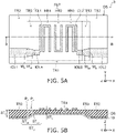
FIGS. 5A and 5B are schematic views showing aplane filter 3 according to a third modification of the embodiment.FIG. 5A is a plan view showing the front surface of the dielectric substrate DS.FIG. 5B is a cross-sectional view along line B-B shown inFIG. 5A . - The
plane filter 3 includes the filter part FLP, the input/output line IOL1, and the input/output line IOL2 provided on the front surface of the dielectric substrate DS. The filter part FLP is provided on the first region TR1. The input/output lines IOL1 and IOL2 are provided on the second region TR2. - As shown in
FIG. 5A , the dielectric substrate DS further includes a third region TR3. The third region TR3 is provided between the first region TR1 and the second region TR2. Theplane filter 3 further includes the connecting line IOLA and the connecting line IOLB extending over the first region TR1 and the third region TR3. - The connecting line IOLA is provided between the first coupling line CL1 and the input/output line IOL1. The connecting line IOLA is connected to the input/output line IOL1 at the boundary between the second region TR2 and the third region TR3. Also, the connecting line IOLA is connected to the first coupling line CL1 in the first region TR1.
- For example, the connecting line IOLA has the width W0 in the Y-direction at the boundary between the second region TR2 and the third region TR3. Also, the connecting line IOLA has the width W0A in the Y-direction on a first region TR. The connecting line IOLA has the width W0A in the Y-direction at the boundary between the first region TR1 and the third region TR3. The width W0A is less than the width W0. The Y-direction width of the connecting line IOLA becomes narrower from the boundary of the second region TR2 and the third region TR3 toward the boundary of the first region TR1 and the third region TR3.
- The connecting line IOLB is provided between the second coupling line CL2 and the input/output line IOL2. The connecting line IOLB is connected to the input/output line IOL2 at the boundary of the second region TR2 and the third region TR3. Also, the connecting line IOLB is connected to the second coupling line CL2 in the first region TR1.
- For example, the connecting line IOLB has the width W0 in the Y-direction at the boundary of the second region TR2 and the third region TR3. Also, the connecting line IOLB has the width W0B in the Y-direction on the first region TR1. Also, the connecting line IOLB has the width W0B in the Y-direction at the boundary of the first region TR1 and the third region TR3. The width W0B is less than the width W0. The Y-direction width of the connecting line IOLB becomes narrower from the boundary of the second region TR2 and the third region TR3 toward the boundary of the first region TR1 and the third region TR3.
- As shown in
FIG. 5B , for example, the dielectric substrate DS has the second thickness ST2 at the boundary of the second region TR2 and the third region TR3. Also, the dielectric substrate DS has the first thickness ST1 at the boundary of the first region TR1 and the third region TR3. In other words, a third thickness ST3 of the third region TR3 becomes thin toward the first region TR1. - For example, the dielectric substrate DS has a third thickness ST3A at a first position P1 in the third region TR3, and has a third thickness ST3B at a second position P2. The first position P1 is positioned between the first region TR1 and the second position P2; and the third thickness ST3A is less than the third thickness ST3B.
- By the configuration described above, for example, the connecting line IOLA and the connecting line IOLB are provided to each have a characteristic impedance of 50 Ω.
- In the example, the reflection of the microwave can be further reduced between the input/output line IOL1 and the first coupling line CL1 and between the input/output line IOL2 and the second coupling line CL2.
- While certain embodiments of the inventions have been described, these embodiments have been presented by way of example only, and are not intended to limit the scope of the inventions. These novel embodiments may be embodied in a variety of other forms; and various omissions, substitutions, and changes may be made without departing from the spirit of the inventions. Such embodiments and their modifications are within the scope and spirit of the inventions, and are within the scope of the inventions described in the claims and their equivalents.
Claims (9)
- A plane filter, comprising:a dielectric substrate;a filter part provided on the dielectric substrate; andan input/output line connected to the filter part on the dielectric substrate,the dielectric substrate including a front surface and a back surface, the back surface being at a side opposite to the front surface, the filter part and the input/output line being provided on the front surface,the dielectric substrate further including a first region and a second region, the filter part being provided in the first region, the input/output line being provided in the second region,the first region having a first thickness in a first direction, the first direction being directed from the back surface toward the front surface,the second region having a second thickness in the first direction, the second thickness being less than the first thickness, the back surface having a step corresponding to a difference between the first thickness and the second thickness.
- The plane filter according to claim 1, whereinthe input/output line extends in a second direction along the front surface of the dielectric substrate; and the filter part includes a first resonator including first to third lines,the first line extending in a third direction along the front surface of the dielectric substrate, the third direction crossing the second direction, the first line including a first end and a second end arranged in this order in the third direction,the second line extending in the third direction, the second line being apart from the first line and facing the first line, the second line including a first end and a second end arranged in this order in the third direction;the third line extending in the second direction, the third line being connected to the second end of the first line and the second end of the second line.
- The plane filter according to claim 2, whereinthe filter part further includes a second resonator including fourth to sixth lines,the fourth line extending in the third direction, the fourth line including a first end and a second end arranged in this order in the third direction,the fifth line extending in the third direction, the fifth line being apart from the fourth line and faces the fourth line, the fifth line including a first end and a second end arranged in this order in the third direction,the sixth line extending in the second direction, the sixth line being connected to the first end of the fourth line and the first end of the fifth line; andthe first resonator and the second resonator are arranged in the second direction and apart from each other, the second line of the first resonator facing the fourth line of the second resonator, the first end of the second line facing the first end of the fourth line, the second end of the second line facing the second end of the fourth line.
- The plane filter according to claim 2, whereinthe first line and the second line have a first width and a second width respectively in the second direction, andthe first width and the second width are less than a width in the third direction of the input/output line.
- The plane filter according to claim 4, whereinthe third line has a third width in the third direction, andthe third width is less than the width in the third direction of the input/output line.
- The plane filter according to claim 4, whereinthe fourth line and the fifth line have a fourth width and a fifth width respectively in the second direction, andthe fourth width and the fifth width are less than the width in the third direction of the input/output line.
- The plane filter according to claim 6, whereinthe sixth line has a sixth width in the third direction, andthe sixth width is less than the width in the third direction of the input/output line.
- The plane filter according to claim 1, whereinthe first resonator is provided between the input/output line and the second resonator,the filter part further includes a coupling line extending in the third direction, the coupling line including a first end and a second end arranged in this order in the third direction, andthe coupling line is positioned between the input/output line and the first resonator, the coupling line being apart from the first line of the first resonator and facing the first line of the first resonator, the first end of the coupling line being connected to the input/output line and facing the first end of the first line, the second end of the coupling line facing the second end of the first line.
- The plane filter according to claim 1, further comprising:a connecting line provided on the first region and linking the input/output line and the filter part,the input/output line and the filter part being arranged in a second direction along the front surface of the dielectric substrate, the input/output line having a seventh width in a third direction along the front surface of the dielectric substrate, the third direction crossing the second direction,the connecting line having an eighth width in the third direction, the eighth width being less than the seventh width.
Applications Claiming Priority (2)
| Application Number | Priority Date | Filing Date | Title |
|---|---|---|---|
| JP2020046515 | 2020-03-17 | ||
| PCT/JP2021/010521 WO2021187457A1 (en) | 2020-03-17 | 2021-03-16 | Planar filter |
Publications (2)
| Publication Number | Publication Date |
|---|---|
| EP4123822A1 true EP4123822A1 (en) | 2023-01-25 |
| EP4123822A4 EP4123822A4 (en) | 2024-04-17 |
Family
ID=77770930
Family Applications (1)
| Application Number | Title | Priority Date | Filing Date |
|---|---|---|---|
| EP21772612.4A Pending EP4123822A4 (en) | 2020-03-17 | 2021-03-16 | PLANE FILTER |
Country Status (4)
| Country | Link |
|---|---|
| US (1) | US12244046B2 (en) |
| EP (1) | EP4123822A4 (en) |
| JP (1) | JP7414959B2 (en) |
| WO (1) | WO2021187457A1 (en) |
Families Citing this family (2)
| Publication number | Priority date | Publication date | Assignee | Title |
|---|---|---|---|---|
| CN115428254B (en) | 2020-08-25 | 2025-06-06 | 株式会社藤仓 | Filter device |
| CN115428255B (en) * | 2020-08-25 | 2025-07-11 | 株式会社藤仓 | Filter device |
Family Cites Families (6)
| Publication number | Priority date | Publication date | Assignee | Title |
|---|---|---|---|---|
| JPH07212111A (en) * | 1994-01-20 | 1995-08-11 | Fujitsu General Ltd | Microstrip circuit |
| JPH09232807A (en) | 1996-02-28 | 1997-09-05 | Ngk Spark Plug Co Ltd | Two band filter |
| US6483404B1 (en) * | 2001-08-20 | 2002-11-19 | Xytrans, Inc. | Millimeter wave filter for surface mount applications |
| US6667549B2 (en) * | 2002-05-01 | 2003-12-23 | Bridgewave Communications, Inc. | Micro circuits with a sculpted ground plane |
| TWI462385B (en) * | 2009-05-26 | 2014-11-21 | Wistron Neweb Corp | Self-matching band-pass filter and related frequency down converter |
| JP2011061296A (en) * | 2009-09-07 | 2011-03-24 | Sharp Corp | High-frequency circuit and receiver |
-
2021
- 2021-03-16 JP JP2022508365A patent/JP7414959B2/en active Active
- 2021-03-16 EP EP21772612.4A patent/EP4123822A4/en active Pending
- 2021-03-16 WO PCT/JP2021/010521 patent/WO2021187457A1/en not_active Ceased
- 2021-03-16 US US17/906,589 patent/US12244046B2/en active Active
Also Published As
| Publication number | Publication date |
|---|---|
| JPWO2021187457A1 (en) | 2021-09-23 |
| JP7414959B2 (en) | 2024-01-16 |
| US20230049841A1 (en) | 2023-02-16 |
| US12244046B2 (en) | 2025-03-04 |
| WO2021187457A1 (en) | 2021-09-23 |
| EP4123822A4 (en) | 2024-04-17 |
Similar Documents
| Publication | Publication Date | Title |
|---|---|---|
| US7429902B2 (en) | Differential transmission line having a curved region with selected radius of curvature | |
| JP4958849B2 (en) | Differential transmission line | |
| EP2979321B1 (en) | A transition between a siw and a waveguide interface | |
| EP1990863B1 (en) | Dual band resonator and dual band filter | |
| EP0978896A2 (en) | Transmission line and transmission line resonator | |
| US12244046B2 (en) | Plane filter | |
| KR101094533B1 (en) | Subsidiary SiB filter and its manufacturing method | |
| KR101577370B1 (en) | Microwave filter | |
| CN110336130A (en) | A kind of dipole filter antenna and electronic equipment | |
| CN219553853U (en) | Printed film radio frequency microstrip band-pass filter | |
| JPH10209720A (en) | Multi-layer mounted MMIC circuit | |
| US9859598B2 (en) | Electronic circuit | |
| CN109994806A (en) | ISGW wideband bandpass filter with dual transfer zero and Wide stop bands | |
| EP1581980B1 (en) | Waveguide e-plane rf bandpass filter with pseudo-elliptic response | |
| JP4411315B2 (en) | Band stop filter | |
| KR102907502B1 (en) | Multilayer low-loss transition structure for wideband applications | |
| KR102933610B1 (en) | Patch antenna reducing spurious radiation and ceramic waveguide filter including the same | |
| CN112909455B (en) | Noise suppression filter and method for manufacturing noise suppression filter | |
| CN119581813B (en) | A dual-passband filter based on SISL | |
| CN110224208B (en) | Differential Filter Microstrip Line Structure for Common Mode Signal Rejection | |
| CN116895926A (en) | Substrate integrated waveguide filter based on self-packaging structure | |
| JP2022114987A (en) | Thin-film substrate circuit | |
| CN117223225A (en) | Antenna backplane with reduced crosstalk and method of making same | |
| KR20210018179A (en) | Electric filter structure |
Legal Events
| Date | Code | Title | Description |
|---|---|---|---|
| STAA | Information on the status of an ep patent application or granted ep patent |
Free format text: STATUS: THE INTERNATIONAL PUBLICATION HAS BEEN MADE |
|
| PUAI | Public reference made under article 153(3) epc to a published international application that has entered the european phase |
Free format text: ORIGINAL CODE: 0009012 |
|
| STAA | Information on the status of an ep patent application or granted ep patent |
Free format text: STATUS: REQUEST FOR EXAMINATION WAS MADE |
|
| 17P | Request for examination filed |
Effective date: 20220916 |
|
| AK | Designated contracting states |
Kind code of ref document: A1 Designated state(s): AL AT BE BG CH CY CZ DE DK EE ES FI FR GB GR HR HU IE IS IT LI LT LU LV MC MK MT NL NO PL PT RO RS SE SI SK SM TR |
|
| DAV | Request for validation of the european patent (deleted) | ||
| DAX | Request for extension of the european patent (deleted) | ||
| A4 | Supplementary search report drawn up and despatched |
Effective date: 20240318 |
|
| RIC1 | Information provided on ipc code assigned before grant |
Ipc: H01P 1/203 20060101AFI20240312BHEP |
|
| RAP1 | Party data changed (applicant data changed or rights of an application transferred) |
Owner name: KABUSHIKI KAISHA TOSHIBA |