EP4123710A1 - Display substrate - Google Patents
Display substrate Download PDFInfo
- Publication number
- EP4123710A1 EP4123710A1 EP20736234.4A EP20736234A EP4123710A1 EP 4123710 A1 EP4123710 A1 EP 4123710A1 EP 20736234 A EP20736234 A EP 20736234A EP 4123710 A1 EP4123710 A1 EP 4123710A1
- Authority
- EP
- European Patent Office
- Prior art keywords
- layer
- fingerprint recognition
- under
- screen fingerprint
- oxide
- Prior art date
- Legal status (The legal status is an assumption and is not a legal conclusion. Google has not performed a legal analysis and makes no representation as to the accuracy of the status listed.)
- Pending
Links
Images

Classifications
-
- G—PHYSICS
- G06—COMPUTING OR CALCULATING; COUNTING
- G06V—IMAGE OR VIDEO RECOGNITION OR UNDERSTANDING
- G06V40/00—Recognition of biometric, human-related or animal-related patterns in image or video data
- G06V40/10—Human or animal bodies, e.g. vehicle occupants or pedestrians; Body parts, e.g. hands
- G06V40/12—Fingerprints or palmprints
- G06V40/13—Sensors therefor
- G06V40/1318—Sensors therefor using electro-optical elements or layers, e.g. electroluminescent sensing
-
- H—ELECTRICITY
- H10—SEMICONDUCTOR DEVICES; ELECTRIC SOLID-STATE DEVICES NOT OTHERWISE PROVIDED FOR
- H10F—INORGANIC SEMICONDUCTOR DEVICES SENSITIVE TO INFRARED RADIATION, LIGHT, ELECTROMAGNETIC RADIATION OF SHORTER WAVELENGTH OR CORPUSCULAR RADIATION
- H10F39/00—Integrated devices, or assemblies of multiple devices, comprising at least one element covered by group H10F30/00, e.g. radiation detectors comprising photodiode arrays
- H10F39/10—Integrated devices
- H10F39/12—Image sensors
- H10F39/198—Contact-type image sensors [CIS]
-
- H—ELECTRICITY
- H10—SEMICONDUCTOR DEVICES; ELECTRIC SOLID-STATE DEVICES NOT OTHERWISE PROVIDED FOR
- H10K—ORGANIC ELECTRIC SOLID-STATE DEVICES
- H10K59/00—Integrated devices, or assemblies of multiple devices, comprising at least one organic light-emitting element covered by group H10K50/00
- H10K59/10—OLED displays
- H10K59/12—Active-matrix OLED [AMOLED] displays
-
- H—ELECTRICITY
- H10—SEMICONDUCTOR DEVICES; ELECTRIC SOLID-STATE DEVICES NOT OTHERWISE PROVIDED FOR
- H10K—ORGANIC ELECTRIC SOLID-STATE DEVICES
- H10K59/00—Integrated devices, or assemblies of multiple devices, comprising at least one organic light-emitting element covered by group H10K50/00
- H10K59/60—OLEDs integrated with inorganic light-sensitive elements, e.g. with inorganic solar cells or inorganic photodiodes
-
- H—ELECTRICITY
- H10—SEMICONDUCTOR DEVICES; ELECTRIC SOLID-STATE DEVICES NOT OTHERWISE PROVIDED FOR
- H10K—ORGANIC ELECTRIC SOLID-STATE DEVICES
- H10K59/00—Integrated devices, or assemblies of multiple devices, comprising at least one organic light-emitting element covered by group H10K50/00
- H10K59/60—OLEDs integrated with inorganic light-sensitive elements, e.g. with inorganic solar cells or inorganic photodiodes
- H10K59/65—OLEDs integrated with inorganic image sensors
-
- H—ELECTRICITY
- H10—SEMICONDUCTOR DEVICES; ELECTRIC SOLID-STATE DEVICES NOT OTHERWISE PROVIDED FOR
- H10K—ORGANIC ELECTRIC SOLID-STATE DEVICES
- H10K2102/00—Constructional details relating to the organic devices covered by this subclass
- H10K2102/301—Details of OLEDs
- H10K2102/302—Details of OLEDs of OLED structures
- H10K2102/3023—Direction of light emission
- H10K2102/3026—Top emission
-
- H—ELECTRICITY
- H10—SEMICONDUCTOR DEVICES; ELECTRIC SOLID-STATE DEVICES NOT OTHERWISE PROVIDED FOR
- H10K—ORGANIC ELECTRIC SOLID-STATE DEVICES
- H10K50/00—Organic light-emitting devices
- H10K50/10—OLEDs or polymer light-emitting diodes [PLED]
- H10K50/11—OLEDs or polymer light-emitting diodes [PLED] characterised by the electroluminescent [EL] layers
-
- H—ELECTRICITY
- H10—SEMICONDUCTOR DEVICES; ELECTRIC SOLID-STATE DEVICES NOT OTHERWISE PROVIDED FOR
- H10K—ORGANIC ELECTRIC SOLID-STATE DEVICES
- H10K50/00—Organic light-emitting devices
- H10K50/80—Constructional details
- H10K50/805—Electrodes
- H10K50/81—Anodes
- H10K50/818—Reflective anodes, e.g. ITO combined with thick metallic layers
-
- H—ELECTRICITY
- H10—SEMICONDUCTOR DEVICES; ELECTRIC SOLID-STATE DEVICES NOT OTHERWISE PROVIDED FOR
- H10K—ORGANIC ELECTRIC SOLID-STATE DEVICES
- H10K50/00—Organic light-emitting devices
- H10K50/80—Constructional details
- H10K50/805—Electrodes
- H10K50/82—Cathodes
- H10K50/822—Cathodes characterised by their shape
-
- H—ELECTRICITY
- H10—SEMICONDUCTOR DEVICES; ELECTRIC SOLID-STATE DEVICES NOT OTHERWISE PROVIDED FOR
- H10K—ORGANIC ELECTRIC SOLID-STATE DEVICES
- H10K50/00—Organic light-emitting devices
- H10K50/80—Constructional details
- H10K50/805—Electrodes
- H10K50/82—Cathodes
- H10K50/828—Transparent cathodes, e.g. comprising thin metal layers
-
- H—ELECTRICITY
- H10—SEMICONDUCTOR DEVICES; ELECTRIC SOLID-STATE DEVICES NOT OTHERWISE PROVIDED FOR
- H10K—ORGANIC ELECTRIC SOLID-STATE DEVICES
- H10K59/00—Integrated devices, or assemblies of multiple devices, comprising at least one organic light-emitting element covered by group H10K50/00
- H10K59/80—Constructional details
- H10K59/805—Electrodes
- H10K59/8051—Anodes
- H10K59/80518—Reflective anodes, e.g. ITO combined with thick metallic layers
-
- H—ELECTRICITY
- H10—SEMICONDUCTOR DEVICES; ELECTRIC SOLID-STATE DEVICES NOT OTHERWISE PROVIDED FOR
- H10K—ORGANIC ELECTRIC SOLID-STATE DEVICES
- H10K59/00—Integrated devices, or assemblies of multiple devices, comprising at least one organic light-emitting element covered by group H10K50/00
- H10K59/80—Constructional details
- H10K59/805—Electrodes
- H10K59/8052—Cathodes
- H10K59/80521—Cathodes characterised by their shape
-
- H—ELECTRICITY
- H10—SEMICONDUCTOR DEVICES; ELECTRIC SOLID-STATE DEVICES NOT OTHERWISE PROVIDED FOR
- H10K—ORGANIC ELECTRIC SOLID-STATE DEVICES
- H10K59/00—Integrated devices, or assemblies of multiple devices, comprising at least one organic light-emitting element covered by group H10K50/00
- H10K59/80—Constructional details
- H10K59/805—Electrodes
- H10K59/8052—Cathodes
- H10K59/80524—Transparent cathodes, e.g. comprising thin metal layers
Definitions
- the present disclosure relates to the technical field of display devices, and particularly to a display substrate with an under-screen fingerprint recognition function.
- a current low-temperature polycrystalline oxide display panel usually comprises a low-temperature polysilicon thin film transistor and an oxide thin-film transistor.
- the low-temperature polysilicon thin film transistor has no threshold voltage drift and is used as a driving transistor.
- the oxide thin film transistor has good switching performance and is used as a switching transistor.
- LTPO technology has been used in watches as power-saving technology for emerging active matrix organic light-emitting diodes (AMOLEDs).
- AMOLEDs active matrix organic light-emitting diodes
- the fingerprint on display technology has been applied to mobile phone terminals.
- the present invention provides a display substrate combining LTPO technology and under-screen fingerprint recognition technology, which can realize an under-screen fingerprint recognition function and a screen power saving function.
- the present invention provides the following technical solutions.
- the present disclosure provides a display substrate comprising:
- light emitted by the organic light emitting layer in the display area is reflected to the oxide of the under-screen fingerprint recognition structure.
- the anode layer totally reflects light.
- the cathode layer semi-reflects light.
- the present disclosure further provides a display substrate comprising:
- the under-screen fingerprint recognition structure comprises a gate electrode and an oxide
- the oxide is a photosensitive element and is used as an inductive sensor of the under-screen fingerprint recognition structure.
- light emitted by the organic light emitting layer in the display area is reflected to the oxide of the under-screen fingerprint recognition structure.
- the anode layer totally reflects light.
- the cathode layer semi-reflects light.
- the inductive sensor of the under-screen fingerprint recognition structure is disposed in a gap of a pixel structure.
- the present disclosure further provides a display substrate comprising:
- the under-screen fingerprint recognition structure further comprises a gate electrode and an oxide, and the oxide is a photosensitive element and is used as an inductive sensor of the under-screen fingerprint recognition structure.
- the anode layer totally reflects light.
- the cathode layer semi-reflects light.
- the present invention provides a display substrate combining LTPO technology and under-screen fingerprint recognition technology, in which light emitted by an organic light-emitting layer is reflected by a finger and then sensed by an inductive sensor in an under-screen fingerprint recognition structure to wake up a screen, thereby realizing an induction function of a built-in fingerprint on display. Furthermore, the organic light-emitting layer is not a functional layer in the under-screen fingerprint recognition structure. Therefore, the organic light-emitting layer can be removed from the under-screen fingerprint recognition structure to allow more light reflected by the finger to enter the inductive sensor, thereby greatly improving light-sensing ability.
- the display substrate manufactured using the LTPO technology can also save screen power.
- location or position relationships indicated by terms such as “center”, “longitudinal”, “transverse”, “length”, “width”, “thickness”, “up”, “down”, “front”, “rear”, “left”, “right”, “vertical”, “horizontal”, “top”, “bottom”, “within”, “outside”, “clockwise”, and “counterclockwise” are location or position relationships based on illustration of the accompanying drawings, are merely used for describing the present disclosure and simplifying the description instead of indicating or implying the indicated apparatuses or elements should have specified locations or be constructed and operated according to specified locations, and Thereof, should not be intercepted as limitations to the present disclosure.
- first and second are used merely for description, but shall not be construed as indicating or implying relative importance or implicitly indicating a number of the indicated technical feature. Hence, the feature defined with “first” and “second” may explicitly or implicitly includes one or more such features.
- a term “a plurality of' means “two or more” unless otherwise specifically limited.
- connection may be a fixed connection, a detachable connection, or an integral connection.
- a connection may be a mechanical connection, an electrical connection, or a mutual communication.
- a connection may be a direct connection or may be an indirect connection by using an intermediate medium.
- a connection may be an internal connection or an interaction between two elements. It may be appreciated by those of ordinary skill in the art that the specific meanings of the aforementioned terms in the present disclosure can be understood depending on specific situations.
- a structure in which a first feature is "on” or “under” a second feature may comprise an embodiment in which the first feature directly contacts the second feature, and may also comprise an embodiment in which the first feature and the second feature are not in direct contact with each other, but are contacted via an additional feature formed therebetween.
- a structure in which a first feature is "on”, “above”, or “on top of” a second feature may comprise an embodiment in which the first feature is right or obliquely “on”, “above”, or “on top of' the second feature, or just means that a sea-level elevation of the first feature is greater than a sea-level elevation of the second feature.
- a structure in which a first feature "under”, “below”, or “on bottom of” a second feature may include an embodiment in which the first feature is right “beneath,” “below,” or “on bottom of” the second feature, and may also comprises an embodiment in which the first feature is right or obliquely “under”, “below”, or “on bottom of” the second feature, or just means that a sea-level elevation of the first feature is less than a sea-level elevation of the second feature.
- FIG. 1 is a schematic structural diagram of a display substrate 1 according to an embodiment of the present invention.
- An embodiment of the present invention provides a display substrate 1, comprising:
- a flexible substrate 30 is the bottommost layer.
- An insulating layer 40 is disposed on a side of the flexible substrate 30.
- the low-temperature polycrystalline oxide structure 101 is disposed on a side of the insulating layer 40 away from the flexible substrate 30.
- the low-temperature polycrystalline oxide structure 101 is configured as a TFT structure comprising a P-si layer 1011, a first gate insulating layer 1012, a gate electrode layer 1013, a first interlayer dielectric layer 1014, and a first source/drain electrode layer 1015.
- a second gate insulating layer 105 is disposed on the low-temperature polycrystalline oxide structure 101.
- a first oxide layer 106 is disposed on the second gate insulating layer 105.
- a second interlayer dielectric layer 107 is disposed on the first oxide layer 106 and covers the second gate insulating layer 105 and the first oxide layer 106.
- a second source/drain electrode layer 108 is disposed on the first oxide layer 106 and the second interlayer dielectric layer 107.
- a flat layer 109 is disposed on the second source/drain electrode layer 108 and covers the second source/drain electrode layer 108 and the second interlayer dielectric layer 107.
- An anode layer 104 is disposed on the flat layer 109.
- a pixel defining layer 110 is disposed on the anode layer 104.
- An organic light-emitting layer 102 is disposed on the pixel defining layer 110.
- a cathode layer 103 is disposed on the organic light-emitting layer 102.
- an insulating layer 111 and a polarizer layer 112 are disposed on the cathode layer 103 by a chemical vapor deposition method, an inkjet printing method, and the like.
- a glass cover 113 is bonded by an adhesive glue to complete packaging.
- the flexible substrate 30, the insulating layer 40, the first gate insulating layer 1012, and the first interlayer dielectric layer 1014 are sequentially stacked.
- the gate electrode layer 1013 is disposed on the first interlayer dielectric layer 1014.
- the second gate insulating layer 105 is disposed on the gate electrode layer 1013 and completely covers the gate electrode layer 1013.
- a second oxide layer 201 is disposed on the second gate insulating layer 105.
- the second interlayer dielectric layer 107 is disposed on the second oxide layer 201.
- the flat layer 109 is disposed on the second interlayer dielectric layer 107.
- the flat layer 109, the second interlayer dielectric layer 107, the second oxide layer 201, the second gate insulating layer 105, and the gate electrode layer 1013 constitute the under-screen fingerprint recognition structure 210.
- the under-screen fingerprint recognition structure 210 does not comprise the cathode layer 103 and the organic light-emitting layer 102.
- the second oxide layer 201 in the under-screen fingerprint recognition structure 210 is a photosensitive element. Therefore, the second oxide layer 201 is used as an inductive sensor of the under-screen fingerprint recognition structure 210.
- the screen can be woken up.
- the under-screen fingerprint recognition structure 210 does not comprise the cathode layer 103 and the organic light-emitting layer 102, more light reflected by the fingerprint will enter the sensing area of the second oxide layer 201, thereby improving light-sensing ability and making a fingerprint on display more sensitive.
- the low-temperature polycrystalline oxide structure 101 and the under-screen fingerprint recognition structure 210 are disposed on a same layer.
- the anode layer 104 has a characteristic of totally reflecting light
- the cathode layer 103 has a characteristic of semi-reflecting light.
- the display substrate 1 comprises the low-temperature polycrystalline oxide structure 101 and the under-screen fingerprint recognition structure 210.
- the under-screen fingerprint recognition structure 210 does not comprise the organic light-emitting layer 102 and the cathode layer 103.
- the second oxide layer 201 in the sensing area of the under-screen fingerprint recognition structure 210 is a photosensitive element. After removing the organic light-emitting layer 102 and the cathode layer 103, more light reflected by the fingerprint enters the sensing area of the second oxide layer 201, thereby improving light-sensing ability of the under-screen fingerprint recognition structure 210.
- FIG. 2 is a schematic structural diagram of another display substrate according to an embodiment of the present invention.
- An embodiment of the present invention provides a display substrate 1, comprising:
- a flexible substrate 30 is the bottommost layer.
- An insulating layer 40 is disposed on a side of the flexible substrate 30.
- the low-temperature polycrystalline oxide structure 101 is disposed on a side of the insulating layer 40 away from the flexible substrate 30.
- the low-temperature polycrystalline oxide structure 101 is configured as a TFT structure comprising a P-si layer 1011, a first gate insulating layer 1012, a gate electrode layer 1013, a first interlayer dielectric layer 1014, and a first source/drain electrode layer 1015.
- a second gate insulating layer 105 is disposed on the low-temperature polycrystalline oxide structure 101.
- a first oxide layer 106 is disposed on the second gate insulating layer 105.
- a second interlayer dielectric layer 107 is disposed on the first oxide layer 106 and covers the second gate insulating layer 105 and the first oxide layer 106.
- a second source/drain electrode layer 108 is disposed on the first oxide layer 106 and the second interlayer dielectric layer 107.
- a flat layer 109 is disposed on the second source/drain electrode layer 108 and covers the second source/drain electrode layer 108 and the second interlayer dielectric layer 107.
- An anode layer 104 is disposed on the flat layer 109.
- a pixel defining layer 110 is disposed on the anode layer 104.
- An organic light-emitting layer 102 is disposed on the pixel defining layer 110.
- a cathode layer 103 is disposed on the organic light-emitting layer 102.
- an insulating layer 111 and a polarizer layer 112 are disposed on the cathode layer 103 by a chemical vapor deposition method, an inkjet printing method, and the like.
- a glass cover 113 is bonded by an adhesive glue to complete packaging.
- the flexible substrate 30, the insulating layer 40, the first gate insulating layer 1012, and the first interlayer dielectric layer 1014 are sequentially stacked.
- the gate electrode layer 1013 is disposed on the first interlayer dielectric layer 1014.
- the second gate insulating layer 105 is disposed on the gate electrode layer 1013 and completely covers the gate electrode layer 1013.
- a second oxide layer 201 is disposed on the second gate insulating layer 105.
- the second interlayer dielectric layer 107 is disposed on the second oxide layer 201.
- the flat layer 109 is disposed on the second interlayer dielectric layer 107.
- the organic light-emitting layer 102 is disposed on the flat layer 109.
- the cathode layer 103 is disposed on the organic light-emitting layer 102.
- Other layers such as an insulating layer 111 and a polarizer layer 112 are disposed on the cathode layer 103 by a chemical vapor deposition method, an inkjet printing method, and the like.
- a glass cover 113 is bonded by an adhesive glue to complete packaging.
- the flat layer 109, the second interlayer dielectric layer 107, the second oxide layer 201, the second gate insulating layer 105, and the gate electrode layer 1013 constitute the under-screen fingerprint recognition structure 210.
- the second oxide layer 201 in the under-screen fingerprint recognition structure 210 is a photosensitive element. Therefore, the second oxide layer 201 is used as an inductive sensor of the under-screen fingerprint recognition structure 210.
- the screen can be woken up.
- the low-temperature polycrystalline oxide structure 101 and the under-screen fingerprint recognition structure 210 are disposed on a same layer.
- the anode layer 104 has a characteristic of totally reflecting light
- the cathode layer 103 has a characteristic of semi-reflecting light.
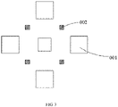
- FIG. 3 is a schematic diagram showing relative positions of induction sensors of an under-screen fingerprint recognition structure.
- inductive sensors 002 of an under-screen fingerprint recognition structure are disposed in gaps of RGB pixels 001, which can save space and improve response times of fingerprint recognition.
- the present invention provides a display substrate combining LTPO technology and under-screen fingerprint recognition technology, in which light emitted by an organic light-emitting layer is reflected by a finger and then sensed by an inductive sensor in an under-screen fingerprint recognition structure to wake up a screen, thereby realizing an induction function of a built-in fingerprint on display. Furthermore, the organic light-emitting layer is not a functional layer in the under-screen fingerprint recognition structure. Therefore, the organic light-emitting layer can be removed from the under-screen fingerprint recognition structure to allow more light reflected by the finger to enter the inductive sensor, thereby greatly improving light-sensing ability.
- the display substrate manufactured using the LTPO technology can also save screen power.
Landscapes
- Engineering & Computer Science (AREA)
- Chemical & Material Sciences (AREA)
- Physics & Mathematics (AREA)
- General Physics & Mathematics (AREA)
- Multimedia (AREA)
- Theoretical Computer Science (AREA)
- Human Computer Interaction (AREA)
- Inorganic Chemistry (AREA)
- Microelectronics & Electronic Packaging (AREA)
- Life Sciences & Earth Sciences (AREA)
- Sustainable Development (AREA)
- Devices For Indicating Variable Information By Combining Individual Elements (AREA)
- Electroluminescent Light Sources (AREA)
Abstract
Description
- The present disclosure relates to the technical field of display devices, and particularly to a display substrate with an under-screen fingerprint recognition function.
- With development of full-screen technology, power-saving technology and fingerprint on display (FOD) technology have become increasingly popular with consumers. With rapid development of the field of display devices, low-temperature polycrystalline oxide (LTPO) display panels have appeared. A current low-temperature polycrystalline oxide display panel usually comprises a low-temperature polysilicon thin film transistor and an oxide thin-film transistor. The low-temperature polysilicon thin film transistor has no threshold voltage drift and is used as a driving transistor. The oxide thin film transistor has good switching performance and is used as a switching transistor. Furthermore, LTPO technology has been used in watches as power-saving technology for emerging active matrix organic light-emitting diodes (AMOLEDs). The fingerprint on display technology has been applied to mobile phone terminals.
- The present invention provides a display substrate combining LTPO technology and under-screen fingerprint recognition technology, which can realize an under-screen fingerprint recognition function and a screen power saving function.
- The present invention provides the following technical solutions.
- The present disclosure provides a display substrate comprising:
- a display area comprising a low-temperature polycrystalline oxide structure, an organic light-emitting layer, a cathode layer, and an anode layer that are sequentially stacked; and
- a fingerprint recognition area comprising an under-screen fingerprint recognition structure, wherein the under-screen fingerprint recognition structure is disposed on a same layer as the low-temperature polycrystalline oxide structure and comprises a gate electrode and an oxide, but does not comprise the cathode layer and the organic light-emitting layer, and the oxide is a photosensitive element and is used as an inductive sensor of the under-screen fingerprint recognition structure in a gap of a pixel structure;
- wherein light emitted from the display area is reflected to the under-screen fingerprint recognition structure in the fingerprint recognition area by a fingerprint.
- In an embodiment, light emitted by the organic light emitting layer in the display area is reflected to the oxide of the under-screen fingerprint recognition structure.
- In an embodiment, the anode layer totally reflects light.
- In an embodiment, the cathode layer semi-reflects light.
- The present disclosure further provides a display substrate comprising:
- a display area comprising a low-temperature polycrystalline oxide structure, an organic light-emitting layer, a cathode layer, and an anode layer that are sequentially stacked; and
- a fingerprint recognition area comprising an under-screen fingerprint recognition structure, wherein the under-screen fingerprint recognition structure is disposed on a same layer as the low-temperature polycrystalline oxide structure and does not comprise the cathode layer and the organic light-emitting layer;
- wherein, light emitted from the display area is reflected to the under-screen fingerprint recognition structure in the fingerprint recognition area by a fingerprint.
- In an embodiment, the under-screen fingerprint recognition structure comprises a gate electrode and an oxide, and the oxide is a photosensitive element and is used as an inductive sensor of the under-screen fingerprint recognition structure.
- In an embodiment, light emitted by the organic light emitting layer in the display area is reflected to the oxide of the under-screen fingerprint recognition structure.
- In an embodiment, the anode layer totally reflects light.
- In an embodiment, the cathode layer semi-reflects light.
- In an embodiment, the inductive sensor of the under-screen fingerprint recognition structure is disposed in a gap of a pixel structure.
- The present disclosure further provides a display substrate comprising:
- a display area comprising a low-temperature polycrystalline oxide structure, an organic light-emitting layer, a cathode layer, and an anode layer that are sequentially stacked; and
- a fingerprint recognition area comprising an under-screen fingerprint recognition structure;
- wherein the low-temperature polycrystalline oxide structure and the under-screen fingerprint recognition structure are disposed on a same layer and share the cathode layer and the organic light-emitting layer, and light emitted from the display area is reflected to the under-screen fingerprint recognition structure in the fingerprint recognition area by a fingerprint.
- In an embodiment, the under-screen fingerprint recognition structure further comprises a gate electrode and an oxide, and the oxide is a photosensitive element and is used as an inductive sensor of the under-screen fingerprint recognition structure.
- In an embodiment, the anode layer totally reflects light.
- In an embodiment, the cathode layer semi-reflects light.
- The present invention provides a display substrate combining LTPO technology and under-screen fingerprint recognition technology, in which light emitted by an organic light-emitting layer is reflected by a finger and then sensed by an inductive sensor in an under-screen fingerprint recognition structure to wake up a screen, thereby realizing an induction function of a built-in fingerprint on display. Furthermore, the organic light-emitting layer is not a functional layer in the under-screen fingerprint recognition structure. Therefore, the organic light-emitting layer can be removed from the under-screen fingerprint recognition structure to allow more light reflected by the finger to enter the inductive sensor, thereby greatly improving light-sensing ability. The display substrate manufactured using the LTPO technology can also save screen power.
- In order to more clearly illustrate technical solutions in embodiments of the present invention, a brief description of accompanying drawings used in description of the embodiments will be given below. Obviously, the accompanying drawings in the following description are merely some embodiments of the present invention. For those skilled in the art, other drawings may be obtained from these accompanying drawings without creative labor.
-
FIG. 1 is a schematic structural diagram of a display substrate according to an embodiment of the present invention. -
FIG. 2 is a schematic structural diagram of another display substrate according to an embodiment of the present invention. -
FIG. 3 is a schematic diagram showing relative positions of induction sensors of an under-screen fingerprint recognition structure. - Technical solutions in embodiments of the present disclosure will be clearly and completely described below in conjunction with accompanying drawings in the embodiments of the present disclosure. It is apparent that the described embodiments are merely a part of the embodiments of the present disclosure and not all embodiments. All other embodiments obtained by those skilled in the art based on the embodiments of the present disclosure without creative labor are within the claimed scope of the present disclosure.
- In the description of the present disclosure, it should be understood that location or position relationships indicated by terms, such as "center", "longitudinal", "transverse", "length", "width", "thickness", "up", "down", "front", "rear", "left", "right", "vertical", "horizontal", "top", "bottom", "within", "outside", "clockwise", and "counterclockwise" are location or position relationships based on illustration of the accompanying drawings, are merely used for describing the present disclosure and simplifying the description instead of indicating or implying the indicated apparatuses or elements should have specified locations or be constructed and operated according to specified locations, and Thereof, should not be intercepted as limitations to the present disclosure. Furthermore, terms such as "first" and "second" are used merely for description, but shall not be construed as indicating or implying relative importance or implicitly indicating a number of the indicated technical feature. Hence, the feature defined with "first" and "second" may explicitly or implicitly includes one or more such features. In the description of the present disclosure, a term "a plurality of' means "two or more" unless otherwise specifically limited.
- In the present disclosure, it should be noted that, unless otherwise explicitly specified or defined, the terms such as "mount", "connect", and "connection" should be interpreted in a broad sense. For example, a connection may be a fixed connection, a detachable connection, or an integral connection. A connection may be a mechanical connection, an electrical connection, or a mutual communication. A connection may be a direct connection or may be an indirect connection by using an intermediate medium. A connection may be an internal connection or an interaction between two elements. It may be appreciated by those of ordinary skill in the art that the specific meanings of the aforementioned terms in the present disclosure can be understood depending on specific situations.
- In the present disclosure, unless otherwise specifically specified or limited, a structure in which a first feature is "on" or "under" a second feature may comprise an embodiment in which the first feature directly contacts the second feature, and may also comprise an embodiment in which the first feature and the second feature are not in direct contact with each other, but are contacted via an additional feature formed therebetween. Furthermore, a structure in which a first feature is "on", "above", or "on top of" a second feature may comprise an embodiment in which the first feature is right or obliquely "on", "above", or "on top of' the second feature, or just means that a sea-level elevation of the first feature is greater than a sea-level elevation of the second feature. A structure in which a first feature "under", "below", or "on bottom of" a second feature may include an embodiment in which the first feature is right "beneath," "below," or "on bottom of" the second feature, and may also comprises an embodiment in which the first feature is right or obliquely "under", "below", or "on bottom of" the second feature, or just means that a sea-level elevation of the first feature is less than a sea-level elevation of the second feature.
- The following description provides different embodiments or examples illustrating various structures of the present invention. In order to simplify the description of the present disclosure, only components and settings of specific examples are described below. They are only examples and are not intended to limit the present invention. Furthermore, reference numerals and/or letters may be repeated in different examples of the present disclosure. Such repetitions are for simplicity and clarity, which per se do not indicate relations among the discussed embodiments and/or settings. Furthermore, the present disclosure provides various examples of specific processes and materials, but those skilled in the art can be aware of application of other processes and/or use of other materials.
- Please refer to
FIG. 1 , which is a schematic structural diagram of adisplay substrate 1 according to an embodiment of the present invention. An embodiment of the present invention provides adisplay substrate 1, comprising: - a
display area 10 comprising a low-temperaturepolycrystalline oxide structure 101, an organic light-emittinglayer 102, acathode layer 103, and ananode layer 104 that are sequentially stacked; and - a
fingerprint recognition area 20 comprising an under-screenfingerprint recognition structure 210, wherein the under-screenfingerprint recognition structure 210 is disposed on a same layer as the low-temperaturepolycrystalline oxide structure 101 and does not comprise thecathode layer 103 and the organic light-emittinglayer 102; - wherein, light emitted from the
display area 10 is reflected to the under-screenfingerprint recognition structure 210 in thefingerprint recognition area 20 by a fingerprint. - In the
display area 10, aflexible substrate 30 is the bottommost layer. An insulatinglayer 40 is disposed on a side of theflexible substrate 30. The low-temperaturepolycrystalline oxide structure 101 is disposed on a side of the insulatinglayer 40 away from theflexible substrate 30. The low-temperaturepolycrystalline oxide structure 101 is configured as a TFT structure comprising a P-si layer 1011, a firstgate insulating layer 1012, agate electrode layer 1013, a firstinterlayer dielectric layer 1014, and a first source/drain electrode layer 1015. A secondgate insulating layer 105 is disposed on the low-temperaturepolycrystalline oxide structure 101. Afirst oxide layer 106 is disposed on the secondgate insulating layer 105. A secondinterlayer dielectric layer 107 is disposed on thefirst oxide layer 106 and covers the secondgate insulating layer 105 and thefirst oxide layer 106. A second source/drain electrode layer 108 is disposed on thefirst oxide layer 106 and the secondinterlayer dielectric layer 107. Aflat layer 109 is disposed on the second source/drain electrode layer 108 and covers the second source/drain electrode layer 108 and the secondinterlayer dielectric layer 107. Ananode layer 104 is disposed on theflat layer 109. Apixel defining layer 110 is disposed on theanode layer 104. An organic light-emittinglayer 102 is disposed on thepixel defining layer 110. Acathode layer 103 is disposed on the organic light-emittinglayer 102. Other layers such as an insulatinglayer 111 and apolarizer layer 112 are disposed on thecathode layer 103 by a chemical vapor deposition method, an inkjet printing method, and the like. Aglass cover 113 is bonded by an adhesive glue to complete packaging. - In the
fingerprint recognition area 20, theflexible substrate 30, the insulatinglayer 40, the firstgate insulating layer 1012, and the firstinterlayer dielectric layer 1014 are sequentially stacked. Thegate electrode layer 1013 is disposed on the firstinterlayer dielectric layer 1014. The secondgate insulating layer 105 is disposed on thegate electrode layer 1013 and completely covers thegate electrode layer 1013. Asecond oxide layer 201 is disposed on the secondgate insulating layer 105. The secondinterlayer dielectric layer 107 is disposed on thesecond oxide layer 201. Theflat layer 109 is disposed on the secondinterlayer dielectric layer 107. Other layers such as an insulatinglayer 111 and apolarizer layer 112 are disposed on theflat layer 109 by a chemical vapor deposition method, an inkjet printing method, and the like. Aglass cover 113 is bonded by an adhesive glue to complete packaging. Theflat layer 109, the secondinterlayer dielectric layer 107, thesecond oxide layer 201, the secondgate insulating layer 105, and thegate electrode layer 1013 constitute the under-screenfingerprint recognition structure 210. - In this embodiment, as shown in
FIG. 1 , the under-screenfingerprint recognition structure 210 does not comprise thecathode layer 103 and the organic light-emittinglayer 102. Thesecond oxide layer 201 in the under-screenfingerprint recognition structure 210 is a photosensitive element. Therefore, thesecond oxide layer 201 is used as an inductive sensor of the under-screenfingerprint recognition structure 210. When light emitted by the organic light-emittinglayer 102 is reflected to a sensing area of thesecond oxide layer 201 by a fingerprint on a screen, the screen can be woken up. Since the under-screenfingerprint recognition structure 210 does not comprise thecathode layer 103 and the organic light-emittinglayer 102, more light reflected by the fingerprint will enter the sensing area of thesecond oxide layer 201, thereby improving light-sensing ability and making a fingerprint on display more sensitive. - As shown in
FIG. 1 , the low-temperaturepolycrystalline oxide structure 101 and the under-screenfingerprint recognition structure 210 are disposed on a same layer. Theanode layer 104 has a characteristic of totally reflecting light, and thecathode layer 103 has a characteristic of semi-reflecting light. - In this embodiment, as shown in
FIG. 1 , thedisplay substrate 1 comprises the low-temperaturepolycrystalline oxide structure 101 and the under-screenfingerprint recognition structure 210. The under-screenfingerprint recognition structure 210 does not comprise the organic light-emittinglayer 102 and thecathode layer 103. Thesecond oxide layer 201 in the sensing area of the under-screenfingerprint recognition structure 210 is a photosensitive element. After removing the organic light-emittinglayer 102 and thecathode layer 103, more light reflected by the fingerprint enters the sensing area of thesecond oxide layer 201, thereby improving light-sensing ability of the under-screenfingerprint recognition structure 210. - Please refer to
FIG. 2 , which is a schematic structural diagram of another display substrate according to an embodiment of the present invention. An embodiment of the present invention provides adisplay substrate 1, comprising: - a
display area 10 comprising a low-temperaturepolycrystalline oxide structure 101, an organic light-emittinglayer 102, acathode layer 103, and ananode layer 104 that are sequentially stacked; and - a
fingerprint recognition area 20 comprising an under-screenfingerprint recognition structure 210; - wherein the low-temperature
polycrystalline oxide structure 101 and the under-screenfingerprint recognition structure 210 are disposed on a same layer and share thecathode layer 103 and the organic light-emittinglayer 102, and light emitted from thedisplay area 10 is reflected to the under-screenfingerprint recognition structure 210 in thefingerprint recognition area 20 by a fingerprint. - In the
display area 10, aflexible substrate 30 is the bottommost layer. An insulatinglayer 40 is disposed on a side of theflexible substrate 30. The low-temperaturepolycrystalline oxide structure 101 is disposed on a side of the insulatinglayer 40 away from theflexible substrate 30. The low-temperaturepolycrystalline oxide structure 101 is configured as a TFT structure comprising a P-si layer 1011, a firstgate insulating layer 1012, agate electrode layer 1013, a firstinterlayer dielectric layer 1014, and a first source/drain electrode layer 1015. A secondgate insulating layer 105 is disposed on the low-temperaturepolycrystalline oxide structure 101. Afirst oxide layer 106 is disposed on the secondgate insulating layer 105. A secondinterlayer dielectric layer 107 is disposed on thefirst oxide layer 106 and covers the secondgate insulating layer 105 and thefirst oxide layer 106. A second source/drain electrode layer 108 is disposed on thefirst oxide layer 106 and the secondinterlayer dielectric layer 107. Aflat layer 109 is disposed on the second source/drain electrode layer 108 and covers the second source/drain electrode layer 108 and the secondinterlayer dielectric layer 107. Ananode layer 104 is disposed on theflat layer 109. Apixel defining layer 110 is disposed on theanode layer 104. An organic light-emittinglayer 102 is disposed on thepixel defining layer 110. Acathode layer 103 is disposed on the organic light-emittinglayer 102. Other layers such as an insulatinglayer 111 and apolarizer layer 112 are disposed on thecathode layer 103 by a chemical vapor deposition method, an inkjet printing method, and the like. Aglass cover 113 is bonded by an adhesive glue to complete packaging. - In the
fingerprint recognition area 20, theflexible substrate 30, the insulatinglayer 40, the firstgate insulating layer 1012, and the firstinterlayer dielectric layer 1014 are sequentially stacked. Thegate electrode layer 1013 is disposed on the firstinterlayer dielectric layer 1014. The secondgate insulating layer 105 is disposed on thegate electrode layer 1013 and completely covers thegate electrode layer 1013. Asecond oxide layer 201 is disposed on the secondgate insulating layer 105. The secondinterlayer dielectric layer 107 is disposed on thesecond oxide layer 201. Theflat layer 109 is disposed on the secondinterlayer dielectric layer 107. The organic light-emittinglayer 102 is disposed on theflat layer 109. Thecathode layer 103 is disposed on the organic light-emittinglayer 102. Other layers such as an insulatinglayer 111 and apolarizer layer 112 are disposed on thecathode layer 103 by a chemical vapor deposition method, an inkjet printing method, and the like. Aglass cover 113 is bonded by an adhesive glue to complete packaging. Theflat layer 109, the secondinterlayer dielectric layer 107, thesecond oxide layer 201, the secondgate insulating layer 105, and thegate electrode layer 1013 constitute the under-screenfingerprint recognition structure 210. - In this embodiment, as shown in
FIG. 2 , thesecond oxide layer 201 in the under-screenfingerprint recognition structure 210 is a photosensitive element. Therefore, thesecond oxide layer 201 is used as an inductive sensor of the under-screenfingerprint recognition structure 210. When light emitted by the organic light-emittinglayer 102 is reflected to a sensing area of thesecond oxide layer 201 by a fingerprint on a screen, the screen can be woken up. As shown inFIG. 2 , the low-temperaturepolycrystalline oxide structure 101 and the under-screenfingerprint recognition structure 210 are disposed on a same layer. Theanode layer 104 has a characteristic of totally reflecting light, and thecathode layer 103 has a characteristic of semi-reflecting light. - Please refer to
FIG. 3 , which is a schematic diagram showing relative positions of induction sensors of an under-screen fingerprint recognition structure. As shown inFIG. 3 , in a structure of a display substrate,inductive sensors 002 of an under-screen fingerprint recognition structure are disposed in gaps ofRGB pixels 001, which can save space and improve response times of fingerprint recognition. - The present invention provides a display substrate combining LTPO technology and under-screen fingerprint recognition technology, in which light emitted by an organic light-emitting layer is reflected by a finger and then sensed by an inductive sensor in an under-screen fingerprint recognition structure to wake up a screen, thereby realizing an induction function of a built-in fingerprint on display. Furthermore, the organic light-emitting layer is not a functional layer in the under-screen fingerprint recognition structure. Therefore, the organic light-emitting layer can be removed from the under-screen fingerprint recognition structure to allow more light reflected by the finger to enter the inductive sensor, thereby greatly improving light-sensing ability. The display substrate manufactured using the LTPO technology can also save screen power.
- The display substrates provided by the embodiments of the present disclosure are described in detail above. The present disclosure uses specific examples to describe principles and embodiments of the present application. The above description of the embodiments is only for helping to understand the technical solutions of the present disclosure and its core ideas. It should be understood by those skilled in the art that they can modify the technical solutions recited in the foregoing embodiments, or replace some of technical features in the foregoing embodiments with equivalents. These modifications or replacements do not cause essence of corresponding technical solutions to depart from the scope of the technical solutions of the embodiments of the present disclosure.
Claims (14)
- A display substrate comprising:a display area comprising a low-temperature polycrystalline oxide structure, an organic light-emitting layer, a cathode layer, and an anode layer that are sequentially stacked; anda fingerprint recognition area comprising an under-screen fingerprint recognition structure, wherein the under-screen fingerprint recognition structure is disposed on a same layer as the low-temperature polycrystalline oxide structure and comprises a gate electrode and an oxide, but does not comprise the cathode layer and the organic light-emitting layer, and the oxide is a photosensitive element and is used as an inductive sensor of the under-screen fingerprint recognition structure in a gap of a pixel structure;wherein light emitted from the display area is reflected to the under-screen fingerprint recognition structure in the fingerprint recognition area by a fingerprint.
- The display substrate as claimed in claim 1, characterized in that light emitted by the organic light-emitting layer in the display area is reflected to the oxide of the under-screen fingerprint recognition structure.
- The display substrate as claimed in claim 2, characterized in that the anode layer totally reflects light.
- The display substrate as claimed in claim 2, characterized in that the cathode layer semi-reflects light.
- A display substrate comprising:a display area comprising a low-temperature polycrystalline oxide structure, an organic light-emitting layer, a cathode layer, and an anode layer that are sequentially stacked; anda fingerprint recognition area comprising an under-screen fingerprint recognition structure, wherein the under-screen fingerprint recognition structure is disposed on a same layer as the low-temperature polycrystalline oxide structure and does not comprise the cathode layer and the organic light-emitting layer;wherein, light emitted from the display area is reflected to the under-screen fingerprint recognition structure in the fingerprint recognition area by a fingerprint.
- The display substrate as claimed in claim 5, characterized in that the under-screen fingerprint recognition structure comprises a gate electrode and an oxide, and the oxide is a photosensitive element and is used as an inductive sensor of the under-screen fingerprint recognition structure.
- The display substrate as claimed in claim 6, characterized in that light emitted by the organic light-emitting layer in the display area is reflected to the oxide of the under-screen fingerprint recognition structure.
- The display substrate as claimed in claim 7, characterized in that the anode layer totally reflects light.
- The display substrate as claimed in claim 7, characterized in that the cathode layer semi-reflects light.
- The display substrate as claimed in claim 5, characterized in that the inductive sensor of the under-screen fingerprint recognition structure is disposed in a gap of a pixel structure.
- A display substrate comprising:a display area comprising a low-temperature polycrystalline oxide structure, an organic light-emitting layer, a cathode layer, and an anode layer that are sequentially stacked; anda fingerprint recognition area comprising an under-screen fingerprint recognition structure;wherein the low-temperature polycrystalline oxide structure and the under-screen fingerprint recognition structure are disposed on a same layer and share the cathode layer and the organic light-emitting layer, and light emitted from the display area is reflected to the under-screen fingerprint recognition structure in the fingerprint recognition area by a fingerprint.
- The display substrate as claimed in claim 11, characterized in that the under-screen fingerprint recognition structure further comprises a gate electrode and an oxide, and the oxide is a photosensitive element and is used as an inductive sensor of the under-screen fingerprint recognition structure.
- The display substrate as claimed in claim 11, characterized in that the anode layer totally reflects light.
- The display substrate as claimed in claim 11, characterized in that the cathode layer semi-reflects light.
Applications Claiming Priority (2)
| Application Number | Priority Date | Filing Date | Title |
|---|---|---|---|
| CN202010190784.4A CN111223910A (en) | 2020-03-18 | 2020-03-18 | Display substrate |
| PCT/CN2020/083252 WO2021184438A1 (en) | 2020-03-18 | 2020-04-03 | Display substrate |
Publications (2)
| Publication Number | Publication Date |
|---|---|
| EP4123710A1 true EP4123710A1 (en) | 2023-01-25 |
| EP4123710A4 EP4123710A4 (en) | 2024-03-13 |
Family
ID=77748287
Family Applications (1)
| Application Number | Title | Priority Date | Filing Date |
|---|---|---|---|
| EP20736234.4A Pending EP4123710A4 (en) | 2020-03-18 | 2020-04-03 | DISPLAY SUBSTRATE |
Country Status (2)
| Country | Link |
|---|---|
| US (1) | US11271052B2 (en) |
| EP (1) | EP4123710A4 (en) |
Families Citing this family (2)
| Publication number | Priority date | Publication date | Assignee | Title |
|---|---|---|---|---|
| WO2022252086A1 (en) | 2021-05-31 | 2022-12-08 | 京东方科技集团股份有限公司 | Light-emitting substrate and display apparatus |
| CN115700051A (en) | 2021-05-31 | 2023-02-03 | 京东方科技集团股份有限公司 | Light emitting substrate and display device |
Family Cites Families (2)
| Publication number | Priority date | Publication date | Assignee | Title |
|---|---|---|---|---|
| CN109685003A (en) * | 2018-12-24 | 2019-04-26 | 武汉华星光电半导体显示技术有限公司 | OLED display panel and the lower optical finger print recognition methods of screen |
| CN109801946B (en) * | 2019-01-30 | 2021-01-26 | 京东方科技集团股份有限公司 | Display panel and display device |
-
2020
- 2020-04-03 US US16/761,532 patent/US11271052B2/en active Active
- 2020-04-03 EP EP20736234.4A patent/EP4123710A4/en active Pending
Also Published As
| Publication number | Publication date |
|---|---|
| US20210296411A1 (en) | 2021-09-23 |
| US11271052B2 (en) | 2022-03-08 |
| EP4123710A4 (en) | 2024-03-13 |
Similar Documents
| Publication | Publication Date | Title |
|---|---|---|
| US11665940B2 (en) | Display substrate for avoiding breaks and preparation method thereof, bonding method of display panel and display apparatus | |
| US20240147809A1 (en) | Transparent oled substrate, transparent display panel, array substrate, display panel, and display device | |
| US11637134B2 (en) | Array substrate, method for manufacturing the same, and display device | |
| US10572042B2 (en) | In cell touch panel, driving method thereof, and display device | |
| US10141525B2 (en) | Light-emitting device, module, and electronic device | |
| US11195863B2 (en) | Display panel having a storage capacitor, manufacturing method the same thereof and display module having the same | |
| CN107342370A (en) | Display panel and display device | |
| US10734608B2 (en) | Display panel and manufacturing method thereof and display device including display panel | |
| US9057903B2 (en) | Flat panel display | |
| CN113066839B (en) | Display panel and display device | |
| US20210408184A1 (en) | Organic light emitting diode display panel and organic light emitting diode display device | |
| CN112802878B (en) | Display panel and display device | |
| US11810515B1 (en) | Pixel driving circuit, display panel and display device | |
| KR20160118122A (en) | Display panel | |
| US11271052B2 (en) | Display substrate comprising low-temperature polycrystalline oxide | |
| US20190051707A1 (en) | Oled touch display panel and oled touch display | |
| WO2021184438A1 (en) | Display substrate | |
| CN114203778A (en) | Active matrix OLED display panel and preparation method thereof | |
| JP2023505359A (en) | Displays and electronic devices | |
| US12572242B2 (en) | Touch display panel and manufacturing method therefor | |
| WO2025200817A1 (en) | Display panel and display device | |
| CN116868702A (en) | Semiconductor device, manufacturing method thereof, and display device | |
| US12563928B2 (en) | Display substrate and electronic device | |
| CN117881235A (en) | Display panel and display device | |
| CN114556566B (en) | A display substrate, display panel and display device |
Legal Events
| Date | Code | Title | Description |
|---|---|---|---|
| STAA | Information on the status of an ep patent application or granted ep patent |
Free format text: STATUS: UNKNOWN |
|
| STAA | Information on the status of an ep patent application or granted ep patent |
Free format text: STATUS: THE INTERNATIONAL PUBLICATION HAS BEEN MADE |
|
| PUAI | Public reference made under article 153(3) epc to a published international application that has entered the european phase |
Free format text: ORIGINAL CODE: 0009012 |
|
| STAA | Information on the status of an ep patent application or granted ep patent |
Free format text: STATUS: REQUEST FOR EXAMINATION WAS MADE |
|
| 17P | Request for examination filed |
Effective date: 20200713 |
|
| AK | Designated contracting states |
Kind code of ref document: A1 Designated state(s): AL AT BE BG CH CY CZ DE DK EE ES FI FR GB GR HR HU IE IS IT LI LT LU LV MC MK MT NL NO PL PT RO RS SE SI SK SM TR |
|
| DAV | Request for validation of the european patent (deleted) | ||
| DAX | Request for extension of the european patent (deleted) | ||
| REG | Reference to a national code |
Ref country code: DE Ref legal event code: R079 Free format text: PREVIOUS MAIN CLASS: H01L0027320000 Ipc: H10K0059650000 |
|
| A4 | Supplementary search report drawn up and despatched |
Effective date: 20240213 |
|
| RIC1 | Information provided on ipc code assigned before grant |
Ipc: G06V 40/13 20220101ALI20240207BHEP Ipc: H10K 59/65 20230101AFI20240207BHEP |
|
| STAA | Information on the status of an ep patent application or granted ep patent |
Free format text: STATUS: EXAMINATION IS IN PROGRESS |
|
| 17Q | First examination report despatched |
Effective date: 20250630 |