EP4123313A1 - Closed-loop microelectromechanical accelerometer with compensation of spurious vibration modes and process for manufacturing a microelectromechanical accelerometer - Google Patents
Closed-loop microelectromechanical accelerometer with compensation of spurious vibration modes and process for manufacturing a microelectromechanical accelerometer Download PDFInfo
- Publication number
- EP4123313A1 EP4123313A1 EP22183947.5A EP22183947A EP4123313A1 EP 4123313 A1 EP4123313 A1 EP 4123313A1 EP 22183947 A EP22183947 A EP 22183947A EP 4123313 A1 EP4123313 A1 EP 4123313A1
- Authority
- EP
- European Patent Office
- Prior art keywords
- sensing
- feedback
- electrode
- plane
- mass
- Prior art date
- Legal status (The legal status is an assumption and is not a legal conclusion. Google has not performed a legal analysis and makes no representation as to the accuracy of the status listed.)
- Granted
Links
Images




Classifications
-
- G—PHYSICS
- G01—MEASURING; TESTING
- G01P—MEASURING LINEAR OR ANGULAR SPEED, ACCELERATION, DECELERATION, OR SHOCK; INDICATING PRESENCE, ABSENCE, OR DIRECTION, OF MOVEMENT
- G01P15/00—Measuring acceleration; Measuring deceleration; Measuring shock, i.e. sudden change of acceleration
- G01P15/02—Measuring acceleration; Measuring deceleration; Measuring shock, i.e. sudden change of acceleration by making use of inertia forces using solid seismic masses
- G01P15/08—Measuring acceleration; Measuring deceleration; Measuring shock, i.e. sudden change of acceleration by making use of inertia forces using solid seismic masses with conversion into electric or magnetic values
- G01P15/125—Measuring acceleration; Measuring deceleration; Measuring shock, i.e. sudden change of acceleration by making use of inertia forces using solid seismic masses with conversion into electric or magnetic values by capacitive pick-up
-
- G—PHYSICS
- G01—MEASURING; TESTING
- G01P—MEASURING LINEAR OR ANGULAR SPEED, ACCELERATION, DECELERATION, OR SHOCK; INDICATING PRESENCE, ABSENCE, OR DIRECTION, OF MOVEMENT
- G01P1/00—Details of instruments
-
- G—PHYSICS
- G01—MEASURING; TESTING
- G01P—MEASURING LINEAR OR ANGULAR SPEED, ACCELERATION, DECELERATION, OR SHOCK; INDICATING PRESENCE, ABSENCE, OR DIRECTION, OF MOVEMENT
- G01P15/00—Measuring acceleration; Measuring deceleration; Measuring shock, i.e. sudden change of acceleration
- G01P15/02—Measuring acceleration; Measuring deceleration; Measuring shock, i.e. sudden change of acceleration by making use of inertia forces using solid seismic masses
- G01P15/08—Measuring acceleration; Measuring deceleration; Measuring shock, i.e. sudden change of acceleration by making use of inertia forces using solid seismic masses with conversion into electric or magnetic values
- G01P15/0802—Details
-
- G—PHYSICS
- G01—MEASURING; TESTING
- G01P—MEASURING LINEAR OR ANGULAR SPEED, ACCELERATION, DECELERATION, OR SHOCK; INDICATING PRESENCE, ABSENCE, OR DIRECTION, OF MOVEMENT
- G01P15/00—Measuring acceleration; Measuring deceleration; Measuring shock, i.e. sudden change of acceleration
- G01P15/02—Measuring acceleration; Measuring deceleration; Measuring shock, i.e. sudden change of acceleration by making use of inertia forces using solid seismic masses
- G01P15/08—Measuring acceleration; Measuring deceleration; Measuring shock, i.e. sudden change of acceleration by making use of inertia forces using solid seismic masses with conversion into electric or magnetic values
- G01P15/13—Measuring acceleration; Measuring deceleration; Measuring shock, i.e. sudden change of acceleration by making use of inertia forces using solid seismic masses with conversion into electric or magnetic values by measuring the force required to restore a proofmass subjected to inertial forces to a null position
- G01P15/131—Measuring acceleration; Measuring deceleration; Measuring shock, i.e. sudden change of acceleration by making use of inertia forces using solid seismic masses with conversion into electric or magnetic values by measuring the force required to restore a proofmass subjected to inertial forces to a null position with electrostatic counterbalancing means
-
- G—PHYSICS
- G01—MEASURING; TESTING
- G01P—MEASURING LINEAR OR ANGULAR SPEED, ACCELERATION, DECELERATION, OR SHOCK; INDICATING PRESENCE, ABSENCE, OR DIRECTION, OF MOVEMENT
- G01P15/00—Measuring acceleration; Measuring deceleration; Measuring shock, i.e. sudden change of acceleration
- G01P15/02—Measuring acceleration; Measuring deceleration; Measuring shock, i.e. sudden change of acceleration by making use of inertia forces using solid seismic masses
- G01P15/08—Measuring acceleration; Measuring deceleration; Measuring shock, i.e. sudden change of acceleration by making use of inertia forces using solid seismic masses with conversion into electric or magnetic values
- G01P2015/0805—Measuring acceleration; Measuring deceleration; Measuring shock, i.e. sudden change of acceleration by making use of inertia forces using solid seismic masses with conversion into electric or magnetic values being provided with a particular type of spring-mass-system for defining the displacement of a seismic mass due to an external acceleration
- G01P2015/0822—Measuring acceleration; Measuring deceleration; Measuring shock, i.e. sudden change of acceleration by making use of inertia forces using solid seismic masses with conversion into electric or magnetic values being provided with a particular type of spring-mass-system for defining the displacement of a seismic mass due to an external acceleration for defining out-of-plane movement of the mass
- G01P2015/0825—Measuring acceleration; Measuring deceleration; Measuring shock, i.e. sudden change of acceleration by making use of inertia forces using solid seismic masses with conversion into electric or magnetic values being provided with a particular type of spring-mass-system for defining the displacement of a seismic mass due to an external acceleration for defining out-of-plane movement of the mass for one single degree of freedom of movement of the mass
- G01P2015/0831—Measuring acceleration; Measuring deceleration; Measuring shock, i.e. sudden change of acceleration by making use of inertia forces using solid seismic masses with conversion into electric or magnetic values being provided with a particular type of spring-mass-system for defining the displacement of a seismic mass due to an external acceleration for defining out-of-plane movement of the mass for one single degree of freedom of movement of the mass the mass being of the paddle type having the pivot axis between the longitudinal ends of the mass, e.g. see-saw configuration
Definitions
- the present invention relates to a closed-loop microelectromechanical accelerometer with compensation of spurious vibration modes and to a process for manufacturing a microelectromechanical accelerometer.
- the monitoring of vibrations in machines of industrial plants is particularly important.
- the early and accurate identification of anomalous vibrations is decisive to avoid not only failures and potentially serious damage to the plants, but also for the correct execution of suitable maintenance interventions, so as to optimize costs and in general maintain efficiency at high levels.
- a problem for this type of applications arises from the fact that monitoring requires high performance not only in terms of sensitivity and noise, but also in terms of bandwidth, as anomalous vibrations may be related to a wide range of phenomena and, consequently, appear on a very broad spectrum.
- accelerometers that are best suited for their characteristics are bulk piezoelectric accelerometers, open-loop capacitive microelectromechanical accelerometers and closed-loop microelectromechanical accelerometers.
- Bulk piezoelectric accelerometers for example, have a very wide band and an optimum dynamic range, but are bulky and expensive and require to be recalibrated relatively frequently, without having the possibility of self-diagnosis procedures. Furthermore, the sensitivity depends significantly on the temperature and generally only sensors of uniaxial type may be produced.
- Open-loop capacitive microelectromechanical accelerometers have the advantage of small size and low cost, without excessively scarifying the band. Beyond a certain limit, however, a tradeoff is to be sought between the bandwidth on the one hand and the noise levels and sensitivity on the other hand. In fact, while the noise tends to increase as the bandwidth increases, to the detriment of the quality of the measurements, the sensitivity decreases quadratically.
- Closed-loop microelectromechanical accelerometers apply feedback forces to cancel the inertial forces acting on a movable mass and maintain the movable mass in proximity to an equilibrium position; the intensity of the control is a measure of the inertial forces that are opposed.
- This solution allows to combine stability, linearity and low noise levels of sensors operating on relatively narrow frequency ranges with a large bandwidth.
- Closed-loop microelectromechanical accelerometers may also be used to manufacture triaxial devices, combining sensing structures of the in-plane and out-of-plane type. Particularly in sensors of the out-of-plane type, however, feedback forces may trigger spurious vibration modes of the movable masses.
- a closed-loop microelectromechanical accelerometer 1 of the out-of-plane type normally comprises a substrate 2 of semiconductor material, a movable mass 3, defined by a plate also of semiconductor material, sensing electrodes 4 and feedback electrodes 5.
- the movable mass 3 has a barycenter G and is connected to the substrate 2 at a fulcrum 6 with an offset with respect to the barycenter G.
- the movable mass 3 is connected so as to be able to rotate, with respect to the substrate 2, around a non-barycentric fulcrum axis F. In the absence of external forces applied, the movable mass 3 is maintained in an equilibrium position, for example parallel to the substrate 2, by flexures not shown here.
- the net force caused by the control may trigger spurious vibration modes, which appear as a torque applied to one end of the movable mass 3 and modify the movement of the movable mass 3 itself.
- the control device has no way of discriminating the cause of the movements of the movable masses and reacts by trying to compensate also the forces caused by the spurious vibration modes, but in doing so equally spurious signal components are introduced which degrade the quality of the measurements.
- the aim of the present invention is to provide a microelectromechanical accelerometer and a process for manufacturing a microelectromechanical accelerometer which allow the described limitations to be overcome or at least mitigated.
- microelectromechanical device and a process for manufacturing a microelectromechanical device are provided, as defined in claims 1 and 14, respectively.
- the microelectromechanical device 10 is a triaxial accelerometer comprising a supporting body 11, an in-plane sensing mass 12, which responds to accelerations in an XY-plane parallel to a face of the supporting body 11, and an out-of-plane sensing mass 13, which responds to accelerations along an out-of-plane sensing axis Z perpendicular to the XY-plane.
- the use in triaxial accelerometers is not to be considered as limiting and it is understood that the invention may equally be used to make uniaxial or biaxial accelerometers with out-of-plane sensing along an axis.
- FIG. 3 illustrates, in a simplified manner, the operation of the accelerometer 10 relative to the sensing of accelerations along the Z-axis.
- the accelerometer 10 in particular, is provided with sensing electrodes 15 and with feedback electrodes 17 capacitively coupled to the out-of-plane sensing mass 13 and comprises a sensing stage 18, a control device 20 and a driving stage 21.
- the sensing stage 18, through the sensing electrodes 15, generates reading signals SR indicative of the angular position of the out-of-plane sensing mass 13 around a fulcrum axis F.
- the control device 20 From the reading signals SR, the control device 20 generates control signals SC which are applied to the feedback electrodes 17 through the driving stage 21 and tend to bring the out-of-plane sensing mass 13 back to an equilibrium position.
- the micromechanical part of the accelerometer 10 relating to the out-of-plane sensing is shown in more detail in Figures 4 and 5 , where the supporting body 11, the out-of-plane sensing mass 13, the sensing electrodes and the feedback electrodes are illustrated in particular.
- the supporting body 11 comprises a substrate 23 of semiconductor material, covered by an insulating layer 24, and a perimeter wall 25, which defines, with the substrate 23, a cavity 27 where the out-of-plane sensing mass 13 is accommodated.
- a cap 28 is bonded to the perimeter wall 25 through an adhesion layer 29, for example glass-frit, and closes the cavity 27.
- the out-of-plane sensing mass 13 is made of semiconductor material, for example polycrystalline silicon.
- the out-of-plane sensing mass 13 is also connected to the supporting body 11 through an anchor 30 and flexures 31, configured to allow rotations of the out-of-plane sensing mass 13 around the fulcrum axis F, which is a non-barycentric axis parallel to a face of the substrate 23 and perpendicular to the out-of-plane sensing axis Z.
- the anchor 30 and the flexures 31 are illustrated only schematically in Figure 5 .
- one end of the out-of-plane sensing mass 13 further away from the anchor 30 is provided with an additional mass 32.
- the sensing electrodes comprise a first group of sensing electrodes facing the first side of the out-of-plane sensing mass and a second group of sensing electrodes facing the second side of the out-of-plane sensing mass.
- the sensing electrodes include a first sensing electrode 15a, a second sensing electrode 15b, a third sensing electrode 15c and a fourth sensing electrode 15d, arranged in pairs symmetrically with respect to the fulcrum axis F so as to obtain differential signals.
- the first sensing electrode 15a and the second sensing electrode 15b are formed on the insulating layer 24 in symmetrical positions with respect to the fulcrum axis F and face a first side 13a of the out-of-plane sensing mass 13 facing the substrate 23.
- the first sensing electrode 15a and the second sensing electrode 15b are capacitively coupled to the out-of-plane sensing mass 13 and electrically insulated from each other.
- the third sensing electrode 15c and the fourth sensing electrode 15d are formed on respective sensing supports 35 in symmetrical positions with respect to the fulcrum axis F and face a second side 13b of the out-of-plane sensing mass 13 opposite to the first side 13a.
- the third sensing electrode 15c and the fourth sensing electrode 15d are arranged in positions corresponding to the positions of the second sensing electrode 15b and of the first sensing electrode 15a, respectively.
- the third sensing electrode 15c and the fourth sensing electrode 15d are also capacitively coupled to the out-of-plane sensing mass 13 and electrically ( Figure 6 ) are insulated from each other and directly connected to the first sensing electrode 15a and to the second sensing electrode 15b, respectively.
- the capacitive coupling varies in a differential manner with respect to the equilibrium position between the first sensing electrode 15a and the third sensing electrode 15c on one side and the second sensing electrode 15b and the fourth sensing electrode 15d on the other side.
- the feedback electrodes comprise a first group of feedback electrodes facing the first side of the out-of-plane sensing mass and a second group of feedback electrodes facing the second side of the out-of-plane sensing mass.
- the feedback electrodes include a first feedback electrode 17a, a second feedback electrode 17b, a third feedback electrode 17c and a fourth feedback electrode 17d, arranged in pairs symmetrically with respect to the fulcrum axis F. More precisely, the first feedback electrode 17a and the second feedback electrode 17b are formed on the insulating layer 24 in symmetrical positions with respect to the fulcrum axis F and face the first side 13a of the out-of-plane feedback mass 13.
- the first feedback electrode 17a and the second feedback electrode 17b are capacitively coupled to the out-of-plane feedback mass 13 and electrically insulated from each other.
- the third feedback electrode 17c and the fourth feedback electrode 17d are formed on respective feedback supports 37 in symmetrical positions with respect to the fulcrum axis F and face the second side 13b of the out-of-plane feedback mass 13.
- the third feedback electrode 17c and the fourth feedback electrode 17d are arranged in positions corresponding to the positions of the second feedback electrode 17b and of the first feedback electrode 17a, respectively.
- the third feedback electrode 17c and the fourth feedback electrode 17d are capacitively coupled to the out-of-plane feedback mass 13 and electrically ( Figure 7 ) are insulated from each other and directly connected to the first feedback electrode 17a and to the second feedback electrode 17b, respectively.
- the feedback electrodes 17a-17d are also in positions which are closer to the anchor 30 with respect to the sensing electrodes 15a-15b.
- the sensing supports 35 and the feedback supports 37 are made of semiconductor material and are anchored to the substrate 20.
- the sensing supports 35 and the feedback supports 37 have respective first structures 35a, 37a, extending from the substrate 20 in a direction parallel to the out-of-plane sensing axis Z through openings 38 in the out-of-plane sensing mass 13; and respective second structures 35b, 37b extending from the respective first structures 35a, 37a in a direction perpendicular to the out-of-plane sensing axis Z.
- the first structures 35a, 37a are anchored to the substrate 23 and are connected to respective conductive lines 40, 41 formed in the insulating layer 24 ( Figures 6 and 7 ).
- the first structures 35a of the sensing supports 35 are connected to respective conductive lines 40, which are insulated from each other.
- the first structures 37a of the feedback supports 37 are connected to respective conductive lines 41, which are insulated from each other.
- the second structures 35b, 37b of the sensing supports 35 and of the feedback supports 37 face the second side 13b of the out-of-plane sensing mass 13, opposite with respect to the substrate 20.
- the third sensing electrode 15c, the fourth sensing electrode 15d, the third feedback electrode 17c and the fourth feedback electrode 17d are arranged between the second structures 35b, 37b of the respective sensing supports 35 and feedback supports 37 and the out-of-plane sensing mass 13.
- Each sensing support 35 is adjacent to and aligned with a respective feedback support 37, with the respective first structures arranged through the same openings 38.
- the second structures 37b of the feedback supports 37 extend from the respective first structures 37a towards the anchor 30; the second structures of the sensing supports 35 extend from the respective first structures 35a in a direction opposite to the anchor 30.
- the feedback electrodes 17a-17d apply electrostatic feedback forces F FB1 , F FB2 to the out-of-plane sensing mass 13 due to the control signals SC supplied by the control device 20 through the driving stage 21 to balance the external forces and bring the out-of-plane sensing mass 13 back to the equilibrium position ( Figure 8 ). Furthermore, for the symmetrical arrangement described, the electrostatic feedback forces F FB1 , F FB2 have zero resultant, even if a feedback torque T FB is applied to the out-of-plane sensing mass 13 around the fulcrum axis F.
- the first feedback electrode 17a and the third feedback electrode 17c are always at an equal distance from the out-of-plane sensing mass 13 (according to the out-of-plane sensing axis Z), regardless of its angular position around the fulcrum axis. Since they are directly connected to each other and are at the same potential, the applied electrostatic feedback forces F FB1 have equal modulus and opposite directions. Similarly, the second feedback electrode 17b and the fourth feedback electrode 17d apply electrostatic feedback forces F FB2 with equal modulus and opposite directions.
- the zero resultant of the electrostatic feedback forces F FB1 , F FB2 is practically unable to trigger spurious vibration modes, which, as discussed, appear in the form of a torque tending to rotate the out-of-plane sensing mass 13 around an axis other than the fulcrum axis F.
- Spurious signal components are also avoided. These signal components are in fact generated by the control device 20 to balance the effects of the spurious vibration modes, which cannot be discriminated from the inertial forces to be measured.
- the zero resultant of the electrostatic feedback forces F FB1 , F FB2 avoids the triggering of spurious vibration modes and, consequently, spurious signal components that would otherwise be indistinguishable from the useful signal.
- the accelerometer according to the invention is therefore advantageous in terms of sensitivity, stability, linearity and bandwidth, as well as having a low cost with respect to sensors of the piezoelectric-type and being rather easily integrable into biaxial or triaxial devices.
- microelectromechanical device 10 of Figures 2-5 may be made through the process described hereinbelow with reference to Figures 9-15 .
- the out-of-plane sensing mass 13, the anchor 30, the sensing supports 35, the feedback supports 37 and the respective sensing and feedback electrodes are obtained from two structural layers epitaxially grown on top of each other, as described in detail hereinbelow.
- a wafer 50 of semiconductor material initially comprises the substrate 23, having the insulating layer 24, for example of silicon oxide, grown thereon.
- a conductive layer not shown in full, for example of polycrystalline silicon is deposited on the insulating layer 24 and shaped to form the first sensing electrode 15a, the second sensing electrode 15b, the first feedback electrode 17a, the second feedback electrode 17b and the conductive lines 40, 41.
- a first sacrificial layer 51 for example of thermally-grown or deposited silicon oxide, is formed on the insulating layer 24 and covers the sensing electrodes 15a, 15b, the feedback electrodes 17a, 17b and the conductive lines 40, 41.
- the first sacrificial layer 51 is selectively etched in positions corresponding to the anchor 30 of the out-of-plane sensing mass 13, to the sensing electrodes 15a, 15b, to the feedback electrodes 17a, 17b and to the conductive lines 40, 41, where the first structures 35a, 37a of the sensing supports 35 and of the feedback supports 37 will be formed later on.
- a first structural layer 55 is grown by epitaxy above the first sacrificial layer 51 from a deposited seed layer 55' and contacts the sensing electrodes 15a, 15b, the feedback electrodes 17a, 17b and the conductive lines 40, 41.
- the first structural layer 55 has a thickness which is determined on the basis of the characteristics of the desired micro-electro-mechanical structures and may be comprised for example between 2 and 80 ⁇ m.
- the first structural layer 55 is planarized and brought to the desired final thickness, for example by CMP (Chemical Mechanical Polishing).
- the first structural layer 55 is etched to define bottom portions of the desired structures and of other regions provided according to the design preferences.
- the anchor 30, the out-of-plane sensing mass 13, the flexures 31, a bottom portion 30' of the anchor 30, the first structures 35a, 37a of the sensing support 35 and of the feedback support 37 and bottom portions 25' of the perimeter wall 25 are formed from the first structural layer 55.
- the wafer 50 is covered by a resist mask not shown (first trench mask) and subject to a dry etching, forming trenches 56, which completely extend through the first structural layer 55.
- trenches are also formed through the portion of the first structural layer 55 intended to form the out-of-plane sensing mass 13, which will have a lattice structure.
- the trenches will also be used in the subsequent steps for removing the sacrificial layer 51. The etching automatically stops on the first sacrificial layer 51.
- a second sacrificial layer 58 for example of TEOS (TetraethylOrthoSilicate), is deposited for a thickness equal to the desired width W of a gap between the out-of-plane sensing mass 13 and the sensing supports 35 and the sensing supports 37.
- the second sacrificial layer 58 partially fills the trenches 56, for example to one third of their depth although this filling, as well as the extent and depth of filling are not important.
- the second sacrificial layer 58 is then planarized.
- the second sacrificial layer 58 is selectively thinned in zones where the third sensing electrode 15c, the fourth sensing electrode 15d, the third feedback electrode 17c and the fourth feedback electrode 15d will have to be subsequently formed.
- a masking layer not shown a masked etching, for example a time-etching, is performed in a per se known manner, to form recesses 60 in positions corresponding to the first sensing electrode 15a, the second sensing electrode 15b, the first feedback electrode 17a, the second feedback electrode 17b.
- the areas intended for other structures of the accelerometer 10 are also delimited, such as the contact structures that limit out-of-plane displacements (bumps).
- the second sacrificial layer 58 is further etched and selectively removed throughout its thickness, using a masking layer not shown (second anchoring mask), forming openings 61.
- the etching of the second sacrificial layer 58 leads to the formation of hard masking regions 58' and automatically terminates on the first epitaxial layer 55.
- the openings 61 are defined between adjacent hard masking regions 58' and, in the illustrated embodiment, are arranged at the end of the out-of-plane sensing mass 13 further away from the fulcrum axis F, on the first structures 35a, 37a of the sensing supports 35 and of the feedback supports 37 and, in general, in zones where it is desired to form connection regions with the first epitaxial layer 55, e.g. the perimeter wall 25. Due to the recesses 60, the hard masking regions 58' have two different thicknesses: a greater thickness equal to that of the second sacrificial layer 58, and a smaller thickness where the recesses 60 are formed.
- a second structural layer 65 is grown, also in this case by epitaxy, for a thickness for example between 2 and 80 ⁇ m.
- the thickness of the second structural layer 65 is related to the desired micro-electro-mechanical structures, including the sensing supports 35 and the feedback supports 37.
- the second structural layer 65 may be thinner than the first structural layer 55, even though the opposite may occur and the invention is not limited to any particular relationship between the thicknesses of the structural layers 55, 65.
- the semiconductor material which during the epitaxial growth fills the recesses 60, forms the third sensing electrode 15c, the fourth sensing electrode 15d, the third feedback electrode 17c and the fourth feedback electrode 17d.
- the second structural layer 65 is planarized and brought to the desired final thickness, for example by CMP (Chemical Mechanical Polishing).
- the second structural layer 65 is etched as shown in Figure 15 .
- the wafer 50 is covered by a resist mask (not illustrated) and subject to a dry etching.
- the portions of the second structural layer 25 not covered by the resist mask are removed throughout the thickness and the etching stops on the hard masking regions 58'.
- the out-of-plane sensing mass 13 (with the additional mass 32 formed from the second structural layer 65), the second structures 35b, 37b of the sensing supports 35 and of the feedback supports 37 and the upper part of the perimeter wall 25 are defined.
- a cap wafer is bonded to the wafer 50 by the adhesion layer 28 and the composite wafer thus obtained is diced to form the accelerometer 10 of Figure 2 .
- Figure 16 shows an electronic system 100 which may be of any type, in particular, but not limited to, a wearable device, such as a watch, a smart bracelet or band; a computer, such as a mainframe, a personal computer, a laptop or a tablet; a smartphone; a digital music player, a digital camera or any other device for processing, storing, transmitting or receiving information.
- the electronic system 100 may be a general purpose or device-embedded processing system, an equipment or a further system.
- the electronic system 100 may be a system for monitoring vibrations in machinery of an industrial plant.
- the electronic system 100 comprises a processing unit 102, memory devices 103, a microelectromechanical gyroscope according to the invention, for example the microelectromechanical gyroscope 1 of Figure 1 , and may also be provided with input/output (I/O) devices 105 (e.g. a keyboard, a pointer or a touch screen), a wireless interface 106, peripherals 107.1, ..., 107.N and possibly further auxiliary devices, not shown here.
- I/O input/output
- the components of the electronic system 100 may be coupled in communication with each other directly and/or indirectly through a bus 108.
- the electronic system 100 may also comprise a battery 109. It should be noted that the scope of the present invention is not limited to embodiments necessarily having one or all the listed devices.
- the processing unit 102 may comprise, for example, one or more microprocessors, microcontrollers and the like, according to the design preferences.
- the memory devices 103 may comprise volatile memory devices and non-volatile memory devices of various kinds, for example SRAM and/or DRAM memories for the volatile-type and solid-state memories, magnetic disks and/or optical disks for the non-volatile type.
- the shape and dimensions of the sensing and feedback electrodes may be freely chosen according to the design preferences.
- the supports for the sensing and feedback electrodes may be adjacent to the sensing mass and extend inwards on the second side.
- the flanks of the out-of-plane sensing mass might be variously shaped according to the design preferences.
Landscapes
- Physics & Mathematics (AREA)
- General Physics & Mathematics (AREA)
- Pressure Sensors (AREA)
Abstract
Description
- The present invention relates to a closed-loop microelectromechanical accelerometer with compensation of spurious vibration modes and to a process for manufacturing a microelectromechanical accelerometer.
- As is known, among the innumerable applications of the accelerometers, in particular microelectromechanical ones, the monitoring of vibrations in machines of industrial plants, such as motors, turbines, pumps and so on is particularly important. The early and accurate identification of anomalous vibrations is decisive to avoid not only failures and potentially serious damage to the plants, but also for the correct execution of suitable maintenance interventions, so as to optimize costs and in general maintain efficiency at high levels.
- A problem for this type of applications arises from the fact that monitoring requires high performance not only in terms of sensitivity and noise, but also in terms of bandwidth, as anomalous vibrations may be related to a wide range of phenomena and, consequently, appear on a very broad spectrum. Among the accelerometers that are best suited for their characteristics are bulk piezoelectric accelerometers, open-loop capacitive microelectromechanical accelerometers and closed-loop microelectromechanical accelerometers. However, all suffer from limitations that make the results not entirely satisfactory.
- Bulk piezoelectric accelerometers, for example, have a very wide band and an optimum dynamic range, but are bulky and expensive and require to be recalibrated relatively frequently, without having the possibility of self-diagnosis procedures. Furthermore, the sensitivity depends significantly on the temperature and generally only sensors of uniaxial type may be produced.
- Open-loop capacitive microelectromechanical accelerometers have the advantage of small size and low cost, without excessively scarifying the band. Beyond a certain limit, however, a tradeoff is to be sought between the bandwidth on the one hand and the noise levels and sensitivity on the other hand. In fact, while the noise tends to increase as the bandwidth increases, to the detriment of the quality of the measurements, the sensitivity decreases quadratically.
- Closed-loop microelectromechanical accelerometers apply feedback forces to cancel the inertial forces acting on a movable mass and maintain the movable mass in proximity to an equilibrium position; the intensity of the control is a measure of the inertial forces that are opposed. This solution allows to combine stability, linearity and low noise levels of sensors operating on relatively narrow frequency ranges with a large bandwidth. Closed-loop microelectromechanical accelerometers may also be used to manufacture triaxial devices, combining sensing structures of the in-plane and out-of-plane type. Particularly in sensors of the out-of-plane type, however, feedback forces may trigger spurious vibration modes of the movable masses.
- As shown schematically in
Figure 1 , a closed-loopmicroelectromechanical accelerometer 1 of the out-of-plane type normally comprises asubstrate 2 of semiconductor material, amovable mass 3, defined by a plate also of semiconductor material, sensingelectrodes 4 andfeedback electrodes 5. Themovable mass 3 has a barycenter G and is connected to thesubstrate 2 at a fulcrum 6 with an offset with respect to the barycenter G. In practice, themovable mass 3 is connected so as to be able to rotate, with respect to thesubstrate 2, around a non-barycentric fulcrum axis F. In the absence of external forces applied, themovable mass 3 is maintained in an equilibrium position, for example parallel to thesubstrate 2, by flexures not shown here. - When an external force causes a displacement of the
accelerometer 1 along an axis Z perpendicular to thesubstrate 2, themovable mass 3 tends to rotate around the fulcrum axis F and the displacements are sesed by thesensing electrodes 4. A control device (not shown) applies electrostatic feedback forces FFB, FFB' through thefeedback electrodes 5 to bring themovable mass 3 back to the equilibrium position and cancel the displacements. However, since the electrostatic feedback forces FFB, FFB' may only be of attractive type, themovable mass 3 is subject to a non-zero net force due to the control. The net force caused by the control may trigger spurious vibration modes, which appear as a torque applied to one end of themovable mass 3 and modify the movement of themovable mass 3 itself. The control device has no way of discriminating the cause of the movements of the movable masses and reacts by trying to compensate also the forces caused by the spurious vibration modes, but in doing so equally spurious signal components are introduced which degrade the quality of the measurements. - The aim of the present invention is to provide a microelectromechanical accelerometer and a process for manufacturing a microelectromechanical accelerometer which allow the described limitations to be overcome or at least mitigated.
- According to the present invention a microelectromechanical device and a process for manufacturing a microelectromechanical device are provided, as defined in
claims 1 and 14, respectively. - For a better understanding of the invention, some embodiments thereof will now be described, purely by way of non-limiting example and with reference to the attached drawings, wherein:
-
Figure 1 is a cross-section through a known microelectromechanical device; -
Figure 2 is a schematic representation of a microelectromechanical accelerometer according to an embodiment of the present invention; -
Figure 3 is a simplified block diagram of a part of the microelectromechanical accelerometer ofFigure 2 ; -
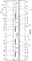
Figure 4 is a top-plan view of a part of the microelectromechanical accelerometer ofFigure 2 , with parts removed for clarity; -
Figure 5 is a cross-section through the microelectromechanical accelerometer ofFigure 2 , taken along line V-V ofFigure 4 ; -
Figure 6 is a simplified electrical diagram of a first detail of the microelectromechanical accelerometer ofFigure 2 ; -
Figure 7 is a simplified electrical diagram of a second detail of the microelectromechanical accelerometer ofFigure 2 ; -
Figure 8 is a schematic side view of the microelectromechanical accelerometer in use; -
Figures 9-15 are cross-sections through a wafer of semiconductor material in subsequent steps of a manufacturing process according to an embodiment of the present invention; and -
Figure 16 is a simplified block diagram of an electronic system incorporating a microelectromechanical device according to the present invention. - With reference to
Figure 2 , a microelectromechanical device according to an embodiment of the present invention is schematically illustrated and indicated with thenumber 10. In the illustrated example, in particular, themicroelectromechanical device 10 is a triaxial accelerometer comprising a supportingbody 11, an in-plane sensing mass 12, which responds to accelerations in an XY-plane parallel to a face of the supportingbody 11, and an out-of-plane sensing mass 13, which responds to accelerations along an out-of-plane sensing axis Z perpendicular to the XY-plane. However, the use in triaxial accelerometers is not to be considered as limiting and it is understood that the invention may equally be used to make uniaxial or biaxial accelerometers with out-of-plane sensing along an axis. -
Figure 3 illustrates, in a simplified manner, the operation of theaccelerometer 10 relative to the sensing of accelerations along the Z-axis. Theaccelerometer 10, in particular, is provided with sensing electrodes 15 and with feedback electrodes 17 capacitively coupled to the out-of-plane sensing mass 13 and comprises asensing stage 18, acontrol device 20 and adriving stage 21. Thesensing stage 18, through the sensing electrodes 15, generates reading signals SR indicative of the angular position of the out-of-plane sensingmass 13 around a fulcrum axis F. From the reading signals SR, thecontrol device 20 generates control signals SC which are applied to the feedback electrodes 17 through thedriving stage 21 and tend to bring the out-of-plane sensing mass 13 back to an equilibrium position. - The micromechanical part of the
accelerometer 10 relating to the out-of-plane sensing is shown in more detail inFigures 4 and5 , where the supportingbody 11, the out-of-plane sensing mass 13, the sensing electrodes and the feedback electrodes are illustrated in particular. The supportingbody 11 comprises asubstrate 23 of semiconductor material, covered by aninsulating layer 24, and aperimeter wall 25, which defines, with thesubstrate 23, acavity 27 where the out-of-plane sensing mass 13 is accommodated. Acap 28 is bonded to theperimeter wall 25 through anadhesion layer 29, for example glass-frit, and closes thecavity 27. - The out-of-
plane sensing mass 13 is made of semiconductor material, for example polycrystalline silicon. The out-of-plane sensing mass 13 is also connected to the supportingbody 11 through ananchor 30 andflexures 31, configured to allow rotations of the out-of-plane sensingmass 13 around the fulcrum axis F, which is a non-barycentric axis parallel to a face of thesubstrate 23 and perpendicular to the out-of-plane sensing axis Z. For ease of representation, theanchor 30 and theflexures 31 are illustrated only schematically inFigure 5 . To increase the imbalance of the out-of-plane sensingmass 13 with respect to the fulcrum axis F and the sensitivity of theaccelerometer 10, one end of the out-of-plane sensingmass 13 further away from theanchor 30 is provided with anadditional mass 32. - The sensing electrodes comprise a first group of sensing electrodes facing the first side of the out-of-plane sensing mass and a second group of sensing electrodes facing the second side of the out-of-plane sensing mass. In detail, the sensing electrodes include a
first sensing electrode 15a, asecond sensing electrode 15b, athird sensing electrode 15c and afourth sensing electrode 15d, arranged in pairs symmetrically with respect to the fulcrum axis F so as to obtain differential signals. More precisely, thefirst sensing electrode 15a and thesecond sensing electrode 15b are formed on the insulatinglayer 24 in symmetrical positions with respect to the fulcrum axis F and face a first side 13a of the out-of-plane sensingmass 13 facing thesubstrate 23. Thefirst sensing electrode 15a and thesecond sensing electrode 15b are capacitively coupled to the out-of-plane sensingmass 13 and electrically insulated from each other. Thethird sensing electrode 15c and thefourth sensing electrode 15d are formed on respective sensing supports 35 in symmetrical positions with respect to the fulcrum axis F and face a second side 13b of the out-of-plane sensing mass 13 opposite to the first side 13a. Thethird sensing electrode 15c and thefourth sensing electrode 15d are arranged in positions corresponding to the positions of thesecond sensing electrode 15b and of thefirst sensing electrode 15a, respectively. Thethird sensing electrode 15c and thefourth sensing electrode 15d are also capacitively coupled to the out-of-plane sensing mass 13 and electrically (Figure 6 ) are insulated from each other and directly connected to thefirst sensing electrode 15a and to thesecond sensing electrode 15b, respectively. Therefore, for the symmetrical arrangement of the sensing electrodes, upon a rotation of the out-of-plane sensingmass 13 around the fulcrum axis F, the capacitive coupling varies in a differential manner with respect to the equilibrium position between thefirst sensing electrode 15a and thethird sensing electrode 15c on one side and thesecond sensing electrode 15b and thefourth sensing electrode 15d on the other side. - Similarly, the feedback electrodes comprise a first group of feedback electrodes facing the first side of the out-of-plane sensing mass and a second group of feedback electrodes facing the second side of the out-of-plane sensing mass. In detail, the feedback electrodes include a
first feedback electrode 17a, asecond feedback electrode 17b, athird feedback electrode 17c and afourth feedback electrode 17d, arranged in pairs symmetrically with respect to the fulcrum axis F. More precisely, thefirst feedback electrode 17a and thesecond feedback electrode 17b are formed on the insulatinglayer 24 in symmetrical positions with respect to the fulcrum axis F and face the first side 13a of the out-of-plane feedback mass 13. Thefirst feedback electrode 17a and thesecond feedback electrode 17b are capacitively coupled to the out-of-plane feedback mass 13 and electrically insulated from each other. Thethird feedback electrode 17c and thefourth feedback electrode 17d are formed on respective feedback supports 37 in symmetrical positions with respect to the fulcrum axis F and face the second side 13b of the out-of-plane feedback mass 13. Thethird feedback electrode 17c and thefourth feedback electrode 17d are arranged in positions corresponding to the positions of thesecond feedback electrode 17b and of thefirst feedback electrode 17a, respectively. Thethird feedback electrode 17c and thefourth feedback electrode 17d are capacitively coupled to the out-of-plane feedback mass 13 and electrically (Figure 7 ) are insulated from each other and directly connected to thefirst feedback electrode 17a and to thesecond feedback electrode 17b, respectively. - The
feedback electrodes 17a-17d are also in positions which are closer to theanchor 30 with respect to thesensing electrodes 15a-15b. - The sensing supports 35 and the feedback supports 37 are made of semiconductor material and are anchored to the
substrate 20. In more detail, the sensing supports 35 and the feedback supports 37 have respectivefirst structures substrate 20 in a direction parallel to the out-of-plane sensing axis Z throughopenings 38 in the out-of-plane sensing mass 13; and respectivesecond structures first structures first structures substrate 23 and are connected to respectiveconductive lines Figures 6 and 7 ). More precisely, thefirst structures 35a of the sensing supports 35 are connected to respectiveconductive lines 40, which are insulated from each other. Thefirst structures 37a of the feedback supports 37 are connected to respectiveconductive lines 41, which are insulated from each other. Thesecond structures plane sensing mass 13, opposite with respect to thesubstrate 20. Thethird sensing electrode 15c, thefourth sensing electrode 15d, thethird feedback electrode 17c and thefourth feedback electrode 17d are arranged between thesecond structures plane sensing mass 13. Eachsensing support 35 is adjacent to and aligned with arespective feedback support 37, with the respective first structures arranged through thesame openings 38. Thesecond structures 37b of the feedback supports 37 extend from the respectivefirst structures 37a towards theanchor 30; the second structures of the sensing supports 35 extend from the respectivefirst structures 35a in a direction opposite to theanchor 30. - The
feedback electrodes 17a-17d apply electrostatic feedback forces FFB1, FFB2 to the out-of-plane sensing mass 13 due to the control signals SC supplied by thecontrol device 20 through the drivingstage 21 to balance the external forces and bring the out-of-plane sensing mass 13 back to the equilibrium position (Figure 8 ). Furthermore, for the symmetrical arrangement described, the electrostatic feedback forces FFB1, FFB2 have zero resultant, even if a feedback torque TFB is applied to the out-of-plane sensing mass 13 around the fulcrum axis F. In fact, thefirst feedback electrode 17a and thethird feedback electrode 17c are always at an equal distance from the out-of-plane sensing mass 13 (according to the out-of-plane sensing axis Z), regardless of its angular position around the fulcrum axis. Since they are directly connected to each other and are at the same potential, the applied electrostatic feedback forces FFB1 have equal modulus and opposite directions. Similarly, thesecond feedback electrode 17b and thefourth feedback electrode 17d apply electrostatic feedback forces FFB2 with equal modulus and opposite directions. The zero resultant of the electrostatic feedback forces FFB1, FFB2 is practically unable to trigger spurious vibration modes, which, as discussed, appear in the form of a torque tending to rotate the out-of-plane sensing mass 13 around an axis other than the fulcrum axis F. Spurious signal components are also avoided. These signal components are in fact generated by thecontrol device 20 to balance the effects of the spurious vibration modes, which cannot be discriminated from the inertial forces to be measured. Ultimately, therefore, the zero resultant of the electrostatic feedback forces FFB1, FFB2 avoids the triggering of spurious vibration modes and, consequently, spurious signal components that would otherwise be indistinguishable from the useful signal. The accelerometer according to the invention is therefore advantageous in terms of sensitivity, stability, linearity and bandwidth, as well as having a low cost with respect to sensors of the piezoelectric-type and being rather easily integrable into biaxial or triaxial devices. - The
microelectromechanical device 10 ofFigures 2-5 may be made through the process described hereinbelow with reference toFigures 9-15 . In practice, the out-of-plane sensing mass 13, theanchor 30, the sensing supports 35, the feedback supports 37 and the respective sensing and feedback electrodes are obtained from two structural layers epitaxially grown on top of each other, as described in detail hereinbelow. - With reference to
Figure 9 , awafer 50 of semiconductor material, for example monocrystalline silicon, initially comprises thesubstrate 23, having the insulatinglayer 24, for example of silicon oxide, grown thereon. A conductive layer not shown in full, for example of polycrystalline silicon, is deposited on the insulatinglayer 24 and shaped to form thefirst sensing electrode 15a, thesecond sensing electrode 15b, thefirst feedback electrode 17a, thesecond feedback electrode 17b and theconductive lines sacrificial layer 51, for example of thermally-grown or deposited silicon oxide, is formed on the insulatinglayer 24 and covers thesensing electrodes feedback electrodes conductive lines sacrificial layer 51 is selectively etched in positions corresponding to theanchor 30 of the out-of-plane sensing mass 13, to thesensing electrodes feedback electrodes conductive lines first structures - Then,
Figure 10 , a firststructural layer 55 is grown by epitaxy above the firstsacrificial layer 51 from a deposited seed layer 55' and contacts thesensing electrodes feedback electrodes conductive lines structural layer 55 has a thickness which is determined on the basis of the characteristics of the desired micro-electro-mechanical structures and may be comprised for example between 2 and 80 µm. After the structural growth, the firststructural layer 55 is planarized and brought to the desired final thickness, for example by CMP (Chemical Mechanical Polishing). - The first
structural layer 55,Figure 11 , is etched to define bottom portions of the desired structures and of other regions provided according to the design preferences. In particular, in this step theanchor 30, the out-of-plane sensing mass 13, theflexures 31, a bottom portion 30' of theanchor 30, thefirst structures sensing support 35 and of thefeedback support 37 and bottom portions 25' of theperimeter wall 25 are formed from the firststructural layer 55. For this purpose, thewafer 50 is covered by a resist mask not shown (first trench mask) and subject to a dry etching, formingtrenches 56, which completely extend through the firststructural layer 55. In this step, trenches (not shown) are also formed through the portion of the firststructural layer 55 intended to form the out-of-plane sensing mass 13, which will have a lattice structure. The trenches will also be used in the subsequent steps for removing thesacrificial layer 51. The etching automatically stops on the firstsacrificial layer 51. - Then,
Figure 12 , a secondsacrificial layer 58, for example of TEOS (TetraethylOrthoSilicate), is deposited for a thickness equal to the desired width W of a gap between the out-of-plane sensing mass 13 and the sensing supports 35 and the sensing supports 37. The secondsacrificial layer 58 partially fills thetrenches 56, for example to one third of their depth although this filling, as well as the extent and depth of filling are not important. The secondsacrificial layer 58 is then planarized. - The second
sacrificial layer 58 is selectively thinned in zones where thethird sensing electrode 15c, thefourth sensing electrode 15d, thethird feedback electrode 17c and thefourth feedback electrode 15d will have to be subsequently formed. For this purpose, by using a masking layer not shown (bump mask) a masked etching, for example a time-etching, is performed in a per se known manner, to formrecesses 60 in positions corresponding to thefirst sensing electrode 15a, thesecond sensing electrode 15b, thefirst feedback electrode 17a, thesecond feedback electrode 17b. With the same bump mask, the areas intended for other structures of theaccelerometer 10 are also delimited, such as the contact structures that limit out-of-plane displacements (bumps). - Subsequently,
Figure 13 , the secondsacrificial layer 58 is further etched and selectively removed throughout its thickness, using a masking layer not shown (second anchoring mask), forming openings 61. The etching of the secondsacrificial layer 58 leads to the formation of hard masking regions 58' and automatically terminates on thefirst epitaxial layer 55. The openings 61 are defined between adjacent hard masking regions 58' and, in the illustrated embodiment, are arranged at the end of the out-of-plane sensing mass 13 further away from the fulcrum axis F, on thefirst structures first epitaxial layer 55, e.g. theperimeter wall 25. Due to therecesses 60, the hard masking regions 58' have two different thicknesses: a greater thickness equal to that of the secondsacrificial layer 58, and a smaller thickness where therecesses 60 are formed. - Subsequently,
Figure 14 , a secondstructural layer 65 is grown, also in this case by epitaxy, for a thickness for example between 2 and 80 µm. The thickness of the secondstructural layer 65 is related to the desired micro-electro-mechanical structures, including the sensing supports 35 and the feedback supports 37. In general, the secondstructural layer 65 may be thinner than the firststructural layer 55, even though the opposite may occur and the invention is not limited to any particular relationship between the thicknesses of thestructural layers recesses 60, forms thethird sensing electrode 15c, thefourth sensing electrode 15d, thethird feedback electrode 17c and thefourth feedback electrode 17d. After the epitaxial growth, the secondstructural layer 65 is planarized and brought to the desired final thickness, for example by CMP (Chemical Mechanical Polishing). - Subsequently, the second
structural layer 65 is etched as shown inFigure 15 . For this purpose, thewafer 50 is covered by a resist mask (not illustrated) and subject to a dry etching. In this step, the portions of the secondstructural layer 25 not covered by the resist mask are removed throughout the thickness and the etching stops on the hard masking regions 58'. - In particular, in this step the out-of-plane sensing mass 13 (with the
additional mass 32 formed from the second structural layer 65), thesecond structures perimeter wall 25 are defined. - Then, the residual portions of the second
sacrificial layer 55 and the firstsacrificial layer 51 are removed, releasing the out-of-plane sensing mass 13. - Finally, a cap wafer is bonded to the
wafer 50 by theadhesion layer 28 and the composite wafer thus obtained is diced to form theaccelerometer 10 ofFigure 2 . -
Figure 16 shows anelectronic system 100 which may be of any type, in particular, but not limited to, a wearable device, such as a watch, a smart bracelet or band; a computer, such as a mainframe, a personal computer, a laptop or a tablet; a smartphone; a digital music player, a digital camera or any other device for processing, storing, transmitting or receiving information. Theelectronic system 100 may be a general purpose or device-embedded processing system, an equipment or a further system. For example, theelectronic system 100 may be a system for monitoring vibrations in machinery of an industrial plant. - The
electronic system 100 comprises aprocessing unit 102,memory devices 103, a microelectromechanical gyroscope according to the invention, for example themicroelectromechanical gyroscope 1 ofFigure 1 , and may also be provided with input/output (I/O) devices 105 (e.g. a keyboard, a pointer or a touch screen), awireless interface 106, peripherals 107.1, ..., 107.N and possibly further auxiliary devices, not shown here. The components of theelectronic system 100 may be coupled in communication with each other directly and/or indirectly through abus 108. Theelectronic system 100 may also comprise abattery 109. It should be noted that the scope of the present invention is not limited to embodiments necessarily having one or all the listed devices. - The
processing unit 102 may comprise, for example, one or more microprocessors, microcontrollers and the like, according to the design preferences. - The
memory devices 103 may comprise volatile memory devices and non-volatile memory devices of various kinds, for example SRAM and/or DRAM memories for the volatile-type and solid-state memories, magnetic disks and/or optical disks for the non-volatile type. - Finally, it is apparent that modifications and variations may be made to the microelectromechanical accelerometer and to the process described, without departing from the scope of the present invention, as defined in the attached claims.
- In particular, the shape and dimensions of the sensing and feedback electrodes may be freely chosen according to the design preferences. Instead of through openings in the out-of-plane sensing mass, the supports for the sensing and feedback electrodes may be adjacent to the sensing mass and extend inwards on the second side. In this case, the flanks of the out-of-plane sensing mass might be variously shaped according to the design preferences.
Claims (16)
- A closed-loop microelectromechanical accelerometer comprising:a supporting body (11) of semiconductor material;an out-of-plane sensing mass (13) of semiconductor material, having a first side (13a) facing the supporting body (11) and a second side (13b) opposite to the first side (13a), wherein the out-of-plane sensing mass (13) is connected to the supporting body (11) to oscillate around a non-barycentric fulcrum axis (F) parallel to the first side (13a) and to the second side (13b) and perpendicular to an out-of-plane sensing axis (Z); andfeedback electrodes (17a-17d), capacitively coupled to the sensing mass (13) and configured to apply opposite electrostatic forces (FFB1, FFB2) and a torque (TFB) around the fulcrum axis (F) to the sensing mass (13);wherein the feedback electrodes (17a-17d) comprise a first group of feedback electrodes (17a, 17b) facing the first side (13a) of the out-of-plane sensing mass (13) and a second group of feedback electrodes (17c, 17d) facing the second side (13b) of the out-of-plane sensing mass (13).
- The accelerometer according to claim 1, wherein the feedback electrodes (17a-17d) comprise:a first feedback electrode (17a) and a second feedback electrode (17b), arranged on the supporting body (11) symmetrically with respect to the fulcrum axis (F) and facing the first side (13a) of the out-of-plane sensing mass (13); anda third feedback electrode (17c) and a fourth feedback electrode (17d), supported by respective feedback supports (37) symmetrically with respect to the fulcrum axis (F) and facing the second side (13b) of the out-of-plane sensing mass (13).
- The accelerometer according to claim 2, wherein the third feedback electrode (17c) and the fourth feedback electrode (17d) are arranged in positions corresponding to positions of the second feedback electrode (17b) and of the first feedback electrode (17a), respectively.
- The accelerometer according to claim 3, wherein the first feedback electrode (17a) and the third feedback electrode (17c) are directly connected to each other and the second feedback electrode (17b) and the fourth feedback electrode (17d) are directly connected to each other and are insulated from the first feedback electrode (17a) and from the third feedback electrode (17c).
- The accelerometer according to any of claims 2 to 4, wherein the feedback supports (37) comprise respective first structures (37a), anchored to the supporting body (11) and extending in a direction parallel to the out-of-plane sensing axis (Z) through openings (38) in the out-of-plane sensing mass (13), and respective second structures (35b, 37b) which extend from the respective first structures (35a, 37a) in a direction perpendicular to the out-of-plane sensing axis (Z) and face the second side (13b) of the out-of-plane sensing mass (13).
- The accelerometer according to claim 5, wherein the feedback supports (37) are of semiconductor material and the first structures (37a) are connected to respective feedback conductive lines (41) formed on the supporting body (11) and insulated from each other.
- The accelerometer according to any of the preceding claims, comprising sensing electrodes (15a-15d), capacitively coupled to the sensing mass (13) and configured to sense an angular position of the sensing mass (13) around the fulcrum axis (F).
- The accelerometer according to claim 7, wherein the sensing electrodes (15a-15d) comprise:a first sensing electrode (15a) and a second sensing electrode (15b), arranged on the supporting body (11) symmetrically with respect to the fulcrum axis (F) and facing the first side (13a) of the out-of-plane sensing mass (13); anda third sensing electrode (15c) and a fourth sensing electrode (15d), supported by respective sensing supports (35) symmetrically with respect to the fulcrum axis (F) and facing the second side (13b) of the out-of-plane sensing mass (13);and wherein the third sensing electrode (15c) and the fourth sensing electrode (15d) are arranged in positions corresponding to positions of the second sensing electrode (15b) and of the first sensing electrode (15a), respectively.
- The accelerometer according to claim 8, wherein the first sensing electrode (15a) and the third sensing electrode (15c) are directly connected to each other and the second sensing electrode (15b) and the fourth sensing electrode (15d) are directly connected to each other and are insulated from the first sensing electrode (15a) and from the third sensing electrode (15c).
- The accelerometer according to claim 8 or 9, wherein the sensing supports (35) comprise respective first structures (35a), anchored to the supporting body (11) and extending in a direction parallel to the out-of-plane sensing axis (Z) through openings (38) in the out-of-plane sensing mass (13), and respective second structures (35b, 35b) which extend from the respective first structures (35a, 35a) in a direction perpendicular to the out-of-plane sensing axis (Z) and face the second side (13b) of the out-of-plane sensing mass (13);
and wherein the sensing supports (35) are of semiconductor material and the first structures (35a) are connected to respective sensing conductive lines (40) formed on the supporting body (11) and insulated from each other. - The accelerometer according to any of claims 7 to 10, comprising:a sensing stage (18), coupled to the sensing electrodes (15) and configured to generate reading signals (SR) indicative of an angular position of the out-of-plane sensing mass (13) around the fulcrum axis (F);a control device (20), configured to supply the feedback electrodes (17) with control signals (SC) generated from the reading signals (SR) and configured to apply the electrostatic forces (FFB1, FFB2) so as to bring the out-of-plane sensing mass (13) back to an equilibrium position in response to inertial forces.
- The accelerometer according to claim 11, wherein the electrostatic forces (FFB1, FFB2) comprise first electrostatic feedback forces (FFB1) having equal modulus and opposite directions and second electrostatic feedback forces (FFB1) having equal modulus and opposite directions.
- An electronic system comprising a processing unit (102) and a microelectromechanical accelerometer (10) according to any of the preceding claims coupled to the processing unit (102).
- A process for manufacturing a closed-loop microelectromechanical accelerometer, comprising:forming an out-of-plane sensing mass (13) of semiconductor material, having a first side (13a) facing a supporting body (11) and a second side (13b) opposite to the first side (13a), wherein the out-of-plane sensing mass (13) is connected to the supporting body (11) to oscillate around a non-barycentric fulcrum axis (F) parallel to the first side (13a) and to the second side (13b) and perpendicular to an out-of-plane sensing axis (Z); andforming feedback electrodes (17a-17d), capacitively coupled to the sensing mass (13) and configured to apply opposite electrostatic forces (FFB1, FFB2) and a torque (TFB) around the fulcrum axis (F) to the sensing mass (13);and wherein forming feedback electrodes (17a-17d) comprises:on a substrate (23) of the supporting body (11), forming a first epitaxial structural layer (55), partially separated from the substrate by an insulating layer (24) with openings;forming a first group of feedback electrodes (17a, 17b) between the substrate (23) and the first side of the out-of-plane sensing mass (13);forming hard masking regions (58') on the first epitaxial structural layer (55) and first openings (61) between adjacent hard masking regions (58');forming a second epitaxial structural layer (65) connected to the first epitaxial structural layer (55) through the first openings (61); andobtaining a second group of feedback electrodes (17c, 17d) from the second epitaxial structural layer (65).
- The process according to claim 14, comprising:forming second openings (38) through the out-of-plane sensing mass (13); andforming feedback supports (37) extending from the substrate (23) through the second openings (38) for the second group of feedback electrodes (17c, 17d);wherein forming feedback supports (37) comprises obtaining first structures (37a) of the feedback supports (37) from the first epitaxial structural layer (55) and obtaining second structures (37b) of the feedback supports (37) from the second epitaxial structural layer (65).
- The process according to claim 14 or 15, wherein forming the out-of-plane sensing mass (13) comprises obtaining the out-of-plane sensing mass (13) from the first epitaxial structural layer (55).
Applications Claiming Priority (1)
| Application Number | Priority Date | Filing Date | Title |
|---|---|---|---|
| IT202100019694 | 2021-07-23 |
Publications (2)
| Publication Number | Publication Date |
|---|---|
| EP4123313A1 true EP4123313A1 (en) | 2023-01-25 |
| EP4123313B1 EP4123313B1 (en) | 2024-11-13 |
Family
ID=78049688
Family Applications (1)
| Application Number | Title | Priority Date | Filing Date |
|---|---|---|---|
| EP22183947.5A Active EP4123313B1 (en) | 2021-07-23 | 2022-07-08 | Closed-loop microelectromechanical accelerometer with compensation of spurious vibration modes and process for manufacturing a microelectromechanical accelerometer |
Country Status (3)
| Country | Link |
|---|---|
| US (1) | US11965906B2 (en) |
| EP (1) | EP4123313B1 (en) |
| CN (2) | CN115700382A (en) |
Families Citing this family (2)
| Publication number | Priority date | Publication date | Assignee | Title |
|---|---|---|---|---|
| EP4123313B1 (en) * | 2021-07-23 | 2024-11-13 | STMicroelectronics S.r.l. | Closed-loop microelectromechanical accelerometer with compensation of spurious vibration modes and process for manufacturing a microelectromechanical accelerometer |
| IT202200014548A1 (en) * | 2022-07-11 | 2024-01-11 | St Microelectronics Srl | SENSING STRUCTURE FOR A MEMS ACCELEROMETER WITH IMPROVED PERFORMANCE AND RELATED MANUFACTURING PROCEDURE |
Citations (4)
| Publication number | Priority date | Publication date | Assignee | Title |
|---|---|---|---|---|
| EP0691542A1 (en) * | 1994-06-29 | 1996-01-10 | Texas Instruments Incorporated | Improved accelerometers |
| US6220096B1 (en) * | 1997-03-20 | 2001-04-24 | Interscience, Inc. | Differential wideband vibration |
| US20080173091A1 (en) * | 2007-01-18 | 2008-07-24 | Freescale Semiconductor, Inc. | Differential capacitive sensor and method of making same |
| US20130333471A1 (en) * | 2012-06-14 | 2013-12-19 | Analog Devices, Inc. | Teeter-Totter Type MEMS Accelerometer with Electrodes on Circuit Wafer |
Family Cites Families (11)
| Publication number | Priority date | Publication date | Assignee | Title |
|---|---|---|---|---|
| US6841992B2 (en) * | 2003-02-18 | 2005-01-11 | Honeywell International, Inc. | MEMS enhanced capacitive pick-off and electrostatic rebalance electrode placement |
| US6935175B2 (en) * | 2003-11-20 | 2005-08-30 | Honeywell International, Inc. | Capacitive pick-off and electrostatic rebalance accelerometer having equalized gas damping |
| DE102009000167B4 (en) * | 2009-01-13 | 2026-02-19 | Robert Bosch Gmbh | Sensor arrangement |
| IT1401001B1 (en) * | 2010-06-15 | 2013-07-05 | Milano Politecnico | MICROELETTROMECHANICAL TRIASSIAL ACCELEROMETER |
| US20150268268A1 (en) * | 2013-06-17 | 2015-09-24 | Freescale Semiconductor, Inc. | Inertial sensor with trim capacitance and method of trimming offset |
| CN103713159B (en) * | 2013-12-27 | 2015-09-16 | 浙江大学 | A kind of closed loop micro-mechanical accelerometer feedback method |
| US10078098B2 (en) * | 2015-06-23 | 2018-09-18 | Analog Devices, Inc. | Z axis accelerometer design with offset compensation |
| TWI663403B (en) * | 2017-05-08 | 2019-06-21 | 日商村田製作所股份有限公司 | Capacitive micromechanical accelerometer and method for performing a self-test in the same |
| IT202000011755A1 (en) | 2020-05-20 | 2021-11-20 | St Microelectronics Srl | MANUFACTURING PROCESS OF A MICRO-ELECTRO-MECHANICAL DEVICE, IN PARTICULAR MOVEMENT SENSOR WITH CAPACITIVE COMMAND/DETECTION, AND RELATED MEMS DEVICE |
| EP4123313B1 (en) * | 2021-07-23 | 2024-11-13 | STMicroelectronics S.r.l. | Closed-loop microelectromechanical accelerometer with compensation of spurious vibration modes and process for manufacturing a microelectromechanical accelerometer |
| EP4187258A1 (en) * | 2021-11-25 | 2023-05-31 | STMicroelectronics S.r.l. | Z-axis microelectromechanical sensor device with improved stress insensitivity |
-
2022
- 2022-07-08 EP EP22183947.5A patent/EP4123313B1/en active Active
- 2022-07-15 US US17/866,378 patent/US11965906B2/en active Active
- 2022-07-21 CN CN202210865253.XA patent/CN115700382A/en active Pending
- 2022-07-21 CN CN202221901673.0U patent/CN218956620U/en active Active
Patent Citations (4)
| Publication number | Priority date | Publication date | Assignee | Title |
|---|---|---|---|---|
| EP0691542A1 (en) * | 1994-06-29 | 1996-01-10 | Texas Instruments Incorporated | Improved accelerometers |
| US6220096B1 (en) * | 1997-03-20 | 2001-04-24 | Interscience, Inc. | Differential wideband vibration |
| US20080173091A1 (en) * | 2007-01-18 | 2008-07-24 | Freescale Semiconductor, Inc. | Differential capacitive sensor and method of making same |
| US20130333471A1 (en) * | 2012-06-14 | 2013-12-19 | Analog Devices, Inc. | Teeter-Totter Type MEMS Accelerometer with Electrodes on Circuit Wafer |
Also Published As
| Publication number | Publication date |
|---|---|
| EP4123313B1 (en) | 2024-11-13 |
| CN115700382A (en) | 2023-02-07 |
| CN218956620U (en) | 2023-05-02 |
| US20230028797A1 (en) | 2023-01-26 |
| US11965906B2 (en) | 2024-04-23 |
Similar Documents
| Publication | Publication Date | Title |
|---|---|---|
| US11808574B2 (en) | Micromechanical detection structure of a MEMS multi-axis gyroscope, with reduced drifts of corresponding electrical parameters | |
| EP2414775B1 (en) | Environmentally robust disc resonator gyroscope | |
| US9513310B2 (en) | High-sensitivity, z-axis micro-electro-mechanical detection structure, in particular for an MEMS accelerometer | |
| US9346670B2 (en) | MEMS device with differential vertical sense electrodes | |
| EP4123313B1 (en) | Closed-loop microelectromechanical accelerometer with compensation of spurious vibration modes and process for manufacturing a microelectromechanical accelerometer | |
| US9383382B2 (en) | Microelectromechanical sensor with out-of-plane sensing and process for manufacturing a microelectromechanical sensor | |
| US7520171B2 (en) | Micro-electromechanical structure with self-compensation of the thermal drifts caused by thermomechanical stress | |
| EP3052901B1 (en) | Inertial and pressure sensors on single chip | |
| US20020170355A1 (en) | Accelerometer strain isolator | |
| CN113697766A (en) | Process for manufacturing a microelectromechanical device and MEMS device | |
| EP4095484B1 (en) | Microelectromechanical device with out-of-plane stopper structure and process for manufacturing a microelectromechanical device | |
| EP3951403A1 (en) | Microelectromechanical sensor device with improved stability to stress | |
| WO2015042702A1 (en) | Mems device including support structure and method of manufacturing | |
| US20240343558A1 (en) | Double layer mems devices and method of manufacture | |
| JP4591000B2 (en) | Semiconductor dynamic quantity sensor and manufacturing method thereof | |
| KR20170004123A (en) | Sensor element and method for manufacturing same | |
| US11933810B2 (en) | Z-axis resonant accelerometer with improved-performance detection structure | |
| Hong et al. | XY and Z-axis capacitive accelerometers packaged in an ultra-clean hermetic environment | |
| US12540952B2 (en) | Microelectromechanical sensor device with active offset compensation | |
| CN217808766U (en) | Micro-electromechanical device | |
| EP4006490B1 (en) | Microelectromechanical gyroscope and method for compensating an output thermal drift in a microelectromechanical gyroscope | |
| EP4421022A1 (en) | Double layer mems devices | |
| CN118108173A (en) | Micro-electromechanical device, manufacturing method thereof, and testing equipment |
Legal Events
| Date | Code | Title | Description |
|---|---|---|---|
| PUAI | Public reference made under article 153(3) epc to a published international application that has entered the european phase |
Free format text: ORIGINAL CODE: 0009012 |
|
| STAA | Information on the status of an ep patent application or granted ep patent |
Free format text: STATUS: THE APPLICATION HAS BEEN PUBLISHED |
|
| AK | Designated contracting states |
Kind code of ref document: A1 Designated state(s): AL AT BE BG CH CY CZ DE DK EE ES FI FR GB GR HR HU IE IS IT LI LT LU LV MC MK MT NL NO PL PT RO RS SE SI SK SM TR |
|
| STAA | Information on the status of an ep patent application or granted ep patent |
Free format text: STATUS: REQUEST FOR EXAMINATION WAS MADE |
|
| 17P | Request for examination filed |
Effective date: 20230725 |
|
| RBV | Designated contracting states (corrected) |
Designated state(s): AL AT BE BG CH CY CZ DE DK EE ES FI FR GB GR HR HU IE IS IT LI LT LU LV MC MK MT NL NO PL PT RO RS SE SI SK SM TR |
|
| GRAP | Despatch of communication of intention to grant a patent |
Free format text: ORIGINAL CODE: EPIDOSNIGR1 |
|
| STAA | Information on the status of an ep patent application or granted ep patent |
Free format text: STATUS: GRANT OF PATENT IS INTENDED |
|
| RIC1 | Information provided on ipc code assigned before grant |
Ipc: G01P 15/13 20060101ALI20240523BHEP Ipc: G01P 15/125 20060101ALI20240523BHEP Ipc: B81B 5/00 20060101ALI20240523BHEP Ipc: G01P 15/08 20060101AFI20240523BHEP |
|
| INTG | Intention to grant announced |
Effective date: 20240607 |
|
| GRAS | Grant fee paid |
Free format text: ORIGINAL CODE: EPIDOSNIGR3 |
|
| GRAA | (expected) grant |
Free format text: ORIGINAL CODE: 0009210 |
|
| STAA | Information on the status of an ep patent application or granted ep patent |
Free format text: STATUS: THE PATENT HAS BEEN GRANTED |
|
| AK | Designated contracting states |
Kind code of ref document: B1 Designated state(s): AL AT BE BG CH CY CZ DE DK EE ES FI FR GB GR HR HU IE IS IT LI LT LU LV MC MK MT NL NO PL PT RO RS SE SI SK SM TR |
|
| REG | Reference to a national code |
Ref country code: GB Ref legal event code: FG4D |
|
| REG | Reference to a national code |
Ref country code: CH Ref legal event code: EP |
|
| REG | Reference to a national code |
Ref country code: IE Ref legal event code: FG4D |
|
| REG | Reference to a national code |
Ref country code: DE Ref legal event code: R096 Ref document number: 602022007637 Country of ref document: DE |
|
| REG | Reference to a national code |
Ref country code: LT Ref legal event code: MG9D |
|
| REG | Reference to a national code |
Ref country code: NL Ref legal event code: MP Effective date: 20241113 |
|
| PG25 | Lapsed in a contracting state [announced via postgrant information from national office to epo] |
Ref country code: HR Free format text: LAPSE BECAUSE OF FAILURE TO SUBMIT A TRANSLATION OF THE DESCRIPTION OR TO PAY THE FEE WITHIN THE PRESCRIBED TIME-LIMIT Effective date: 20241113 Ref country code: IS Free format text: LAPSE BECAUSE OF FAILURE TO SUBMIT A TRANSLATION OF THE DESCRIPTION OR TO PAY THE FEE WITHIN THE PRESCRIBED TIME-LIMIT Effective date: 20250313 Ref country code: PT Free format text: LAPSE BECAUSE OF FAILURE TO SUBMIT A TRANSLATION OF THE DESCRIPTION OR TO PAY THE FEE WITHIN THE PRESCRIBED TIME-LIMIT Effective date: 20250313 |
|
| PG25 | Lapsed in a contracting state [announced via postgrant information from national office to epo] |
Ref country code: FI Free format text: LAPSE BECAUSE OF FAILURE TO SUBMIT A TRANSLATION OF THE DESCRIPTION OR TO PAY THE FEE WITHIN THE PRESCRIBED TIME-LIMIT Effective date: 20241113 Ref country code: NL Free format text: LAPSE BECAUSE OF FAILURE TO SUBMIT A TRANSLATION OF THE DESCRIPTION OR TO PAY THE FEE WITHIN THE PRESCRIBED TIME-LIMIT Effective date: 20241113 |
|
| REG | Reference to a national code |
Ref country code: AT Ref legal event code: MK05 Ref document number: 1742065 Country of ref document: AT Kind code of ref document: T Effective date: 20241113 |
|
| PG25 | Lapsed in a contracting state [announced via postgrant information from national office to epo] |
Ref country code: BG Free format text: LAPSE BECAUSE OF FAILURE TO SUBMIT A TRANSLATION OF THE DESCRIPTION OR TO PAY THE FEE WITHIN THE PRESCRIBED TIME-LIMIT Effective date: 20241113 |
|
| PG25 | Lapsed in a contracting state [announced via postgrant information from national office to epo] |
Ref country code: ES Free format text: LAPSE BECAUSE OF FAILURE TO SUBMIT A TRANSLATION OF THE DESCRIPTION OR TO PAY THE FEE WITHIN THE PRESCRIBED TIME-LIMIT Effective date: 20241113 |
|
| PG25 | Lapsed in a contracting state [announced via postgrant information from national office to epo] |
Ref country code: NO Free format text: LAPSE BECAUSE OF FAILURE TO SUBMIT A TRANSLATION OF THE DESCRIPTION OR TO PAY THE FEE WITHIN THE PRESCRIBED TIME-LIMIT Effective date: 20250213 |
|
| PG25 | Lapsed in a contracting state [announced via postgrant information from national office to epo] |
Ref country code: LV Free format text: LAPSE BECAUSE OF FAILURE TO SUBMIT A TRANSLATION OF THE DESCRIPTION OR TO PAY THE FEE WITHIN THE PRESCRIBED TIME-LIMIT Effective date: 20241113 Ref country code: AT Free format text: LAPSE BECAUSE OF FAILURE TO SUBMIT A TRANSLATION OF THE DESCRIPTION OR TO PAY THE FEE WITHIN THE PRESCRIBED TIME-LIMIT Effective date: 20241113 Ref country code: GR Free format text: LAPSE BECAUSE OF FAILURE TO SUBMIT A TRANSLATION OF THE DESCRIPTION OR TO PAY THE FEE WITHIN THE PRESCRIBED TIME-LIMIT Effective date: 20250214 |
|
| PG25 | Lapsed in a contracting state [announced via postgrant information from national office to epo] |
Ref country code: PL Free format text: LAPSE BECAUSE OF FAILURE TO SUBMIT A TRANSLATION OF THE DESCRIPTION OR TO PAY THE FEE WITHIN THE PRESCRIBED TIME-LIMIT Effective date: 20241113 |
|
| PG25 | Lapsed in a contracting state [announced via postgrant information from national office to epo] |
Ref country code: RS Free format text: LAPSE BECAUSE OF FAILURE TO SUBMIT A TRANSLATION OF THE DESCRIPTION OR TO PAY THE FEE WITHIN THE PRESCRIBED TIME-LIMIT Effective date: 20250213 |
|
| PG25 | Lapsed in a contracting state [announced via postgrant information from national office to epo] |
Ref country code: SM Free format text: LAPSE BECAUSE OF FAILURE TO SUBMIT A TRANSLATION OF THE DESCRIPTION OR TO PAY THE FEE WITHIN THE PRESCRIBED TIME-LIMIT Effective date: 20241113 |
|
| PG25 | Lapsed in a contracting state [announced via postgrant information from national office to epo] |
Ref country code: DK Free format text: LAPSE BECAUSE OF FAILURE TO SUBMIT A TRANSLATION OF THE DESCRIPTION OR TO PAY THE FEE WITHIN THE PRESCRIBED TIME-LIMIT Effective date: 20241113 |
|
| PG25 | Lapsed in a contracting state [announced via postgrant information from national office to epo] |
Ref country code: EE Free format text: LAPSE BECAUSE OF FAILURE TO SUBMIT A TRANSLATION OF THE DESCRIPTION OR TO PAY THE FEE WITHIN THE PRESCRIBED TIME-LIMIT Effective date: 20241113 |
|
| PG25 | Lapsed in a contracting state [announced via postgrant information from national office to epo] |
Ref country code: RO Free format text: LAPSE BECAUSE OF FAILURE TO SUBMIT A TRANSLATION OF THE DESCRIPTION OR TO PAY THE FEE WITHIN THE PRESCRIBED TIME-LIMIT Effective date: 20241113 |
|
| PG25 | Lapsed in a contracting state [announced via postgrant information from national office to epo] |
Ref country code: SK Free format text: LAPSE BECAUSE OF FAILURE TO SUBMIT A TRANSLATION OF THE DESCRIPTION OR TO PAY THE FEE WITHIN THE PRESCRIBED TIME-LIMIT Effective date: 20241113 |
|
| PG25 | Lapsed in a contracting state [announced via postgrant information from national office to epo] |
Ref country code: CZ Free format text: LAPSE BECAUSE OF FAILURE TO SUBMIT A TRANSLATION OF THE DESCRIPTION OR TO PAY THE FEE WITHIN THE PRESCRIBED TIME-LIMIT Effective date: 20241113 |
|
| PG25 | Lapsed in a contracting state [announced via postgrant information from national office to epo] |
Ref country code: IT Free format text: LAPSE BECAUSE OF FAILURE TO SUBMIT A TRANSLATION OF THE DESCRIPTION OR TO PAY THE FEE WITHIN THE PRESCRIBED TIME-LIMIT Effective date: 20241113 |
|
| REG | Reference to a national code |
Ref country code: DE Ref legal event code: R097 Ref document number: 602022007637 Country of ref document: DE |
|
| PG25 | Lapsed in a contracting state [announced via postgrant information from national office to epo] |
Ref country code: SE Free format text: LAPSE BECAUSE OF FAILURE TO SUBMIT A TRANSLATION OF THE DESCRIPTION OR TO PAY THE FEE WITHIN THE PRESCRIBED TIME-LIMIT Effective date: 20241113 |
|
| PLBE | No opposition filed within time limit |
Free format text: ORIGINAL CODE: 0009261 |
|
| STAA | Information on the status of an ep patent application or granted ep patent |
Free format text: STATUS: NO OPPOSITION FILED WITHIN TIME LIMIT |
|
| PGFP | Annual fee paid to national office [announced via postgrant information from national office to epo] |
Ref country code: DE Payment date: 20250620 Year of fee payment: 4 |
|
| 26N | No opposition filed |
Effective date: 20250814 |
|
| REG | Reference to a national code |
Ref country code: CH Ref legal event code: H13 Free format text: ST27 STATUS EVENT CODE: U-0-0-H10-H13 (AS PROVIDED BY THE NATIONAL OFFICE) Effective date: 20260224 |
|
| PG25 | Lapsed in a contracting state [announced via postgrant information from national office to epo] |
Ref country code: LU Free format text: LAPSE BECAUSE OF NON-PAYMENT OF DUE FEES Effective date: 20250708 |
|
| REG | Reference to a national code |
Ref country code: BE Ref legal event code: MM Effective date: 20250731 |
|
| PG25 | Lapsed in a contracting state [announced via postgrant information from national office to epo] |
Ref country code: BE Free format text: LAPSE BECAUSE OF NON-PAYMENT OF DUE FEES Effective date: 20250731 |
|
| PG25 | Lapsed in a contracting state [announced via postgrant information from national office to epo] |
Ref country code: FR Free format text: LAPSE BECAUSE OF NON-PAYMENT OF DUE FEES Effective date: 20250731 |
|
| PG25 | Lapsed in a contracting state [announced via postgrant information from national office to epo] |
Ref country code: CH Free format text: LAPSE BECAUSE OF NON-PAYMENT OF DUE FEES Effective date: 20250731 |