EP4121783B1 - Power electronics circuitry having high-power busbar with controllable resistance - Google Patents
Power electronics circuitry having high-power busbar with controllable resistance Download PDFInfo
- Publication number
- EP4121783B1 EP4121783B1 EP20715288.5A EP20715288A EP4121783B1 EP 4121783 B1 EP4121783 B1 EP 4121783B1 EP 20715288 A EP20715288 A EP 20715288A EP 4121783 B1 EP4121783 B1 EP 4121783B1
- Authority
- EP
- European Patent Office
- Prior art keywords
- power electronics
- electronics circuitry
- busbar
- conductive path
- pattern
- Prior art date
- Legal status (The legal status is an assumption and is not a legal conclusion. Google has not performed a legal analysis and makes no representation as to the accuracy of the status listed.)
- Active
Links
Images


Classifications
-
- G—PHYSICS
- G01—MEASURING; TESTING
- G01R—MEASURING ELECTRIC VARIABLES; MEASURING MAGNETIC VARIABLES
- G01R1/00—Details of instruments or arrangements of the types included in groups G01R5/00 - G01R13/00 and G01R31/00
- G01R1/20—Modifications of basic electric elements for use in electric measuring instruments; Structural combinations of such elements with such instruments
- G01R1/203—Resistors used for electric measuring, e.g. decade resistors standards, resistors for comparators, series resistors, shunts
Definitions
- the present disclosure relates to the field of continuous monitoring of electric components, such as power electronic components.
- the disclosure proposes a busbar with controllable resistance that allows convenient current measurements.
- a busbar 100 with the example structure shown in figure 1 may be used.
- the depicted busbar 100 is composed of two planar conductors or conductive layers, shown as parallel plates 10, 20 separated by a distance d of the order of hundreds of micrometers. For visibility, the distance d has been enlarged in figure 1 .
- the external side of each plate comprises an input area 11, 21 and an output area 12, 22, within which it is suitable to connect a current source or current consumer, e.g., by welding, soldering, clamping means or mechanical connectors of the fixed or detachable type.
- a source-side device (not shown) is connected at the input areas 11, 21 at the left-hand edge of the busbar and a load-side device (not shown) is connected at the output areas 12, 22 at the right-hand edge of the busbar.
- a first current A 10 flows through the upper plate 10
- a second current A 20 flows through the lower plate 20; the orientation of the hollow arrows representing these currents refer to a reference polarity of each current rather than suggesting that the current is unidirectional at all times.
- a busbar is designed to have small resistance, so as to limit thermal losses, and very small inductance.
- a reduced inductance means that the inductive response to a sudden change in the circuit characteristics - as may result from an overvoltage, discharge, short-circuit or the like - is less pronounced, and will thereby protect the connected PEBBs. This is also valid for busbars designed to transfer direct current.
- US5300917A discloses a junction box apparatus for a vehicle.
- the junction box apparatus comprises a shunt busbar and test points.
- the shunt busbar which may be manu-factured by stamping an electrical conductor from flat copper or brass stock, comprises a body portion, two pairs of male terminals for coupling the shunt busbar in a current loop. A load and a power supply can be placed in the current loop.
- a comparator is connected to the terminals across the shunt busbar.
- Shunt-based current monitoring is available for some low-power applications but has not been successfully upscaled to the high-power case. It would be desirable to generalize this robust and relatively simple monitoring technique to PEBB applications.
- One objective is to make available shunt-based current monitoring for PEBB applications. It is a particular objective to propose a busbar allowing such current monitoring.
- a busbar comprising a first conductive layer with an input area and an output area, wherein the conductive layer has a machined pattern defining a meandering conductive path between the input area and output area.
- the machined pattern increases the resistance of the conductive path in a controlled fashion.
- the increase in resistance is achieved without increasing the outer dimensions of the busbar.
- the conductive path from the input area 11 to the output area 12 of the upper plate 10 of the busbar 100 shown in figure 1 is straight and therefore less resistive than an imaginary meandering conductive path in the same plate 10.
- a further advantage of the invention is that the busbar can be manufactured in a simple fashion by manipulation of a conventional planar busbar for PEBBs.
- a still further advantage in comparison with the use of a Rogowski coil that no delicate measuring components, such as an integrator circuit, are needed for the measurement as such.
- power electronics circuitry which comprises: the busbar; a direct-current capacitor connected at the input area of the busbar; a semiconductor device connected at the output area of the busbar; and a current monitoring arrangement adapted to sense a voltage drop over said meandering conductive path.
- the conductive path is one through which the current from the input area to the output area must pass; alternatively, the conductive path is one of several paths in a group which represents all possible paths from the input area to the output area.
- the necessary structural modification may be very limited or even non-existent; in fact, the identification of an input/output area in the sense of the claims may refer to an intended use.
- the conductive path is meandering if it comprises at least one meandering section or portion.
- the machined pattern if it penetrates all the way through the busbar layer, may alternatively be referred to as a slot pattern.
- All references to "a/an/the element, apparatus, component, means, step, etc.” are to be interpreted openly as referring to at least one instance of the element, apparatus, component, means, step, etc., unless explicitly stated otherwise.
- the steps of any method disclosed herein do not have to be performed in the exact order disclosed, unless explicitly stated.
- Busbars according to the present invention which differ from the state of the art mainly by the presence of the machined pattern, may have same or similar generic properties as the busbar shown in figure 1 .
- busbars according to the present invention may include one, two or more conductive layers. The layers may be separated by a void (e.g., air, insulating gas, pressurized or at atmospheric pressure) or an insulating layer. Alternatively or additionally, the placement of the input and output areas 11, 21, 21, 22 may be different, such as on the edge side (i.e., laterally) or extending around the edge of the plate. The width-to-length ratio of the busbar may differ from that suggested in figure 1 .
- Figure 2 is a top view of a conductive layer 10 in a busbar with a machined pattern, according an embodiment of the present invention.
- the machined pattern 13 is composed of six slots (vertically oriented in figure 2 ) in a baffle-like arrangement. It may be said to define a meandering conductive path, in which five vertical segments can be discerned between nearby slots of the machined pattern 13. The conductive path is therefore noticeably longer than the distance from the input area 11 to the output area 12.
- the machined pattern 13 in figure 2 defines a conductive path that is at least twice as long as said distance, which in itself may double the resistance compared to a conductive layer without any machined pattern. Additionally, the conductive path is narrower for the most part than the straight current path on a pattern-free conductive layer, which normally increases the resistance.
- the machined pattern 13 may be a chemically or photochemically machined pattern, preferably an etched pattern, a laser-cut pattern or a waterjet-cut pattern.
- the machined pattern 13 may penetrate through the first conductive layer. In particular, it may be composed of cut-through slots.
- the width of the machined pattern 13 may be approximately 1 mm or less; in other embodiments, the width of the machined pattern 13 may be less than 3 mm or less than 2 mm.
- Machined patterns which define a conductive path with parallel adjacent opposite sections may be advantageous since they avoid an uncontrolled inductance increase when the resistance is brought to increase by the addition of the machined pattern.
- consecutive vertical segments of the conductive path according to figure 2 will convey oppositely directed currents.
- the provision of the machined pattern increases the resistance between the input area 11 and the output area 12 by a factor greater than or equal to a concomitant inductance increase.
- k R ⁇ k L applies. It is recalled that the factors k R , k L can be determined by theoretical calculation or simulation.
- busbar While it is clearly possible to manufacture a busbar according to the invention by starting from a pattern-free busbar layer and adding the machined pattern subsequently, the invention does not require this specific sequencing; rather, the pattern may be present from the earliest stages of the manufacturing process.
- the conductive path may be at least 110%, preferably at least 125%, preferably at least 150%, preferably 2 times, preferably 5 times or preferably 10 times as long as the distance from the input area 11 to the output area 12.
- FIG 3 is a top view of a conductive layer 10 in a busbar according an embodiment of the present invention.
- the conductive layer 10 has a machined pattern 13 defining four parallel conductive paths as well as connection sites 15, 16 allowing the sensing of a voltage drop over the portion of the conductive path that extends between the connection sites 15, 16. From the input area 11, which is common to all four paths, each path passes through a common portion 14 followed by a respective meandering portion that ends in a respective one of the four output areas 12.
- the machined pattern 13 not only comprises slots (vertically oriented in figure 3 ) in baffle-like arrangements but also slots (horizontally oriented in figure 3 ) which delimit one meandering portion of a conductive path from an adjacent one.
- the common portion 14 may be said to be substantially straight in the sense that it allows current to flow substantially along a straight line connecting the input area 11 and the beginning of the meandering portion of each conductive path.
- Each conductive path comprises an upstream 15 and a downstream 16 connection site, respectively located at the beginning and end of the meandering portion.
- the voltage drop over the meandering portion can be determined by electrically connecting the poles of a voltmeter or equivalent circuitry between the connection sites 15, 16, as will be discussed with reference to figure 4 .
- the section of the conductive path joining the two connection sites 15, 16 is approximately 3.7 times as long as the distance between the connection sites 15, 16.
- a corresponding section of the conductive path may be at least 2 times, preferably 5 times, preferably 10 times as long as the distance between the connection sites. This is advantageous since the connection leads of the voltmeter can be kept reasonably short.
- Figure 4 is a top view of a conductive layer 10 belonging to a two-layer busbar according a further embodiment of the present invention.
- the conductive layer 10 has a machined pattern 13 which defines four parallel conductive paths.
- figure 4 shows a capacitor 401 having its two poles connected to the input area 11 of the shown conductive layer 10 and to an input area 21 of a second conductive layer (not shown) of the busbar.
- the two input areas 11, 21 may be suitable for connecting a capacitor 401 serving as a direct-current capacitor for intermediate storage of electric energy that may be supplied via conductors and/or for smoothing purposes.
- Figure 4 further shows four semiconductor devices 402, which are connected between a respective output area 12 of the shown conductive layer 10 and an output area 22 of the second conductive layer (not shown).
- a first circuit composed of: the input area 11 in the first conductive layer 10 - the straight portion of the first conductive path - the meandering portion of the first conductive path - the first output area 12a of the first conductive layer 10 - the first semiconductor device 402a, the first output area 22a of the second conductive layer (not shown) - a conductive path of the second conductive layer (not shown) - the input area 21 of the second conductive layer (not shown).
- the conductive layer 10 illustrated in figure 4 comprises a single dedicated connection site 15 for each conductive path, namely, the upstream connection site.
- the respective output areas 12 are used additionally as downstream conductive site, that is, for connecting one pole of the measurement equipment.
- the downstream conductive site coincides with the output area 12.
- Figure 4 further shows a first example current monitoring arrangement comprising resistors R in , R f and an operational amplifier 403 configured to perform non-inverting amplification of the voltage drop between the first upstream connection site 15a and the first output area 12a.
- a theoretical gain factor may be equal to 1 + R f / R in .
- the current monitoring arrangement further comprises a sensor 404 for reading the amplified output of the operational amplifier 403.
- similar current monitoring arrangements may be provided at the second, third and fourth conductive paths on the first conductive layer 10.
- the current monitoring arrangements may be used to monitor derived electric quantities as well.
- the value of a capacitor connected to the busbar 100, such as the capacitor 401 may be monitored on the basis of the measured current.
- the inventors furthermore envisage a second example current monitoring arrangement, which may replace the first example current monitoring arrangement but otherwise be connected in the same manner, to the upstream connection site 15 and the output area 12.
- the second example current monitoring arrangement is configured to separate low-frequency and high-frequency components of the measured voltage drop into separate branches of circuitry. This may be achieved by letting measurements on the low-frequency components primarily rely on the resistive properties of the conductive layer 10, whereas measurements on the high-frequency components may be based on inductive phenomena.
- the two signals picked up in this manner may undergo low-pass and high-pass filtering, respectively, and optional gain calibration before they are summed together, to form a complete frequency representation of the voltage drop signal.
- the second example current monitoring arrangement may be more sophisticated to implement but may provide greater accuracy and a more even output over the studied frequency range.
- Figure 5 illustrates, in accordance with a further embodiment, a machined pattern 13 on a conductive layer 10 of a busbar for providing a meandering conductive path.
- figure 6 shows a conductive layer 10 with a machined pattern 13 having a mere two vertical slots.
- the slots of the machined pattern 13 define a conductive path that is not only slightly longer than an imaginary straight line between the input area 11 and output area 12, but also significantly narrower in its central segment.
- Connection sites 15 and 16 are provided to allow connection of measurement circuitry for monitoring the voltage drop along the central segment.
- figure 7 shows a machined pattern 13 on a conductive layer 10 of a busbar for providing a meandering conductive path that includes at least one retrograde segment.
- the conductive path between the input area 11 and the output area 12 comprises a meandering portion which begins at the upstream connection site 15 and ends at the downstream connection site 16.
- the conductive path comprises a first segment oriented in an approximate northwest direction in the plane of figure 7 , i.e., one where the flowing current approaches the input area 11 again.
- the first segment is follows by a second segment, in which the current flows in an approximate south-southeast direction, and a third segment that is vertically oriented.
- the conductive pattern continues through on the right-hand half of the conductive pattern 13, where a vertical fourth segment is follows by a north-northeast fifth segment, a southeast sixth segment.
- a vertical fourth segment is follows by a north-northeast fifth segment, a southeast sixth segment.
- current will be forced geometrically closer to the input area 11 and away from the output area 12, that is, away from the general direction of travel.
- the first and sixth segments may be referred to as retrograde segments.
- Machined patterns which define one or more retrograde segments are advantageous since the connection sites 15, 16 can be placed with a small geometric separation even though they are joined by a long portion of the conductive path. This is space-saving and/or helps reduce the length of the connection lines towards the measurement circuitry.
- a busbar according to any of the described embodiments has a nominal current of at least 10 A, such as at least 100 A.
- the resistance of the busbar may range from 20 to 20 000 ⁇ , such as 250 to 20 000 ⁇ , or preferably 50 to 500 ⁇ . In cases where multiple parallel conductive paths are provided, the resistance values apply for one conductive path.
- the busbar has a nominal current of at least 400 A and a resistance of 1 to 500 ⁇ , preferably 10 to 100 ⁇ , for one conductive path. Even for the highest resistance values, the losses due to current monitoring is of the order of tens of watts.
Landscapes
- Physics & Mathematics (AREA)
- General Physics & Mathematics (AREA)
- Measuring Instrument Details And Bridges, And Automatic Balancing Devices (AREA)
Description
- The present disclosure relates to the field of continuous monitoring of electric components, such as power electronic components. In particular, the disclosure proposes a busbar with controllable resistance that allows convenient current measurements.
- To identify a failure of a power electronic device early, the currents flowing to and from the device may be monitored. It is oftentimes preferred in high-power applications to monitor the currents contactlessly, such as by providing connection lines of the device with a Rogowski coil or Hall-effect sensor, both of which utilize inductive phenomena. For examples, see [1] S. Mocevic et al., "Comparison between desaturation sensing and Rogowski coil current sensing for shortcircuit protection of 1.2 kV, 300 A SiC MOSFET module", proceedings of the 2018 IEEE Applied Power Electronics Conference and Exposition (APEC), San Antonio 2018, pages 2666-2672 and [2] S. J. Nibir et al., "Wideband contactless current sensing using hybrid magnetoresistor-Rogowski sensor in high frequency power electronic converters", ibid., pages 904-908.
- To connect power-electronic building blocks (PEBBs), a
busbar 100 with the example structure shown infigure 1 may be used. The depictedbusbar 100 is composed of two planar conductors or conductive layers, shown asparallel plates figure 1 . The external side of each plate comprises aninput area output area - In one example use case, a source-side device (not shown) is connected at the
input areas output areas upper plate 10, and a second current A20 flows through thelower plate 20; the orientation of the hollow arrows representing these currents refer to a reference polarity of each current rather than suggesting that the current is unidirectional at all times.
Conventionally, a busbar is designed to have small resistance, so as to limit thermal losses, and very small inductance. A reduced inductance means that the inductive response to a sudden change in the circuit characteristics - as may result from an overvoltage, discharge, short-circuit or the like - is less pronounced, and will thereby protect the connected PEBBs. This is also valid for busbars designed to transfer direct current.
US5300917A discloses a junction box apparatus for a vehicle. The junction box apparatus comprises a shunt busbar and test points. The shunt busbar, which may be manu-factured by stamping an electrical conductor from flat copper or brass stock, comprises a body portion, two pairs of male terminals for coupling the shunt busbar in a current loop. A load and a power supply can be placed in the current loop. A comparator is connected to the terminals across the shunt busbar.
Shunt-based current monitoring is available for some low-power applications but has not been successfully upscaled to the high-power case. It would be desirable to generalize this robust and relatively simple monitoring technique to PEBB applications. - One objective is to make available shunt-based current monitoring for PEBB applications. It is a particular objective to propose a busbar allowing such current monitoring.
- In the invention according to independent claim 1, there is provided a busbar comprising a first conductive layer with an input area and an output area, wherein the conductive layer has a machined pattern defining a meandering conductive path between the input area and output area.
- Because the meandering conductive path is longer than a straight conductive path directly from the input to the output area, the machined pattern increases the resistance of the conductive path in a controlled fashion. The increase in resistance is achieved without increasing the outer dimensions of the busbar. For comparison, the conductive path from the
input area 11 to theoutput area 12 of theupper plate 10 of thebusbar 100 shown infigure 1 is straight and therefore less resistive than an imaginary meandering conductive path in thesame plate 10. By providing the busbar with a desired resistance, it becomes possible to monitor the current flowing through the busbar by monitoring a voltage drop along the conductive path. - A further advantage of the invention is that the busbar can be manufactured in a simple fashion by manipulation of a conventional planar busbar for PEBBs. A still further advantage in comparison with the use of a Rogowski coil that no delicate measuring components, such as an integrator circuit, are needed for the measurement as such.
- In the invention, power electronics circuitry is provided, which comprises: the busbar; a direct-current capacitor connected at the input area of the busbar; a semiconductor device connected at the output area of the busbar; and a current monitoring arrangement adapted to sense a voltage drop over said meandering conductive path.
- Generally, all terms used in the claims are to be interpreted according to their ordinary meaning in the technical field, unless explicitly defined otherwise herein. The conductive path is one through which the current from the input area to the output area must pass; alternatively, the conductive path is one of several paths in a group which represents all possible paths from the input area to the output area. To render an input or output area suitable for its purpose of connecting a current source or current consumer, the necessary structural modification may be very limited or even non-existent; in fact, the identification of an input/output area in the sense of the claims may refer to an intended use. In the sense of the claims, moreover, the conductive path is meandering if it comprises at least one meandering section or portion. The machined pattern, if it penetrates all the way through the busbar layer, may alternatively be referred to as a slot pattern. All references to "a/an/the element, apparatus, component, means, step, etc." are to be interpreted openly as referring to at least one instance of the element, apparatus, component, means, step, etc., unless explicitly stated otherwise. The steps of any method disclosed herein do not have to be performed in the exact order disclosed, unless explicitly stated.
- Aspects and embodiments are now described, by way of example, with reference to the accompanying drawings, on which:
-
figure 1 is a perspective view of a busbar with two conductive layers according to the state of the art; -
figure 2 is a top view of a conductive layer in a busbar with a machined pattern, according an embodiment of the present invention; -
figure 3 is a top view of a conductive layer in a busbar according an embodiment of the present invention comprising a machined pattern defining four parallel conductive paths as well as connection sites allowing the sensing of a voltage drop over the conductive path; -
figure 4 is a top view of a conductive layer in a busbar according an embodiment of the present invention comprising a machined pattern defining four parallel conductive paths as well as connection sites to which example measurement circuitry is connected; and -
figures 5 to 7 are top views of a conductive layer in a busbar, occasionally with connection sites for voltage sensing, according to further embodiments of the present invention. - The aspects of the present disclosure will now be described more fully with reference to the accompanying drawings, on which certain embodiments of the invention are shown. These aspects may, however, be embodied in many different forms and should not be construed as limiting; rather, the disclosed embodiments are provided by way of example so that this disclosure will be thorough and complete, and to fully convey the scope of all aspects of invention to those skilled in the art. Like numbers refer to like elements throughout the description.
-
Figure 1 , which has been briefly discussed in a previous section of this disclosure, shows a two-layer busbar 100 according to the state of the art. Busbars according to the present invention, which differ from the state of the art mainly by the presence of the machined pattern, may have same or similar generic properties as the busbar shown infigure 1 . In terms of possible further differences, busbars according to the present invention may include one, two or more conductive layers. The layers may be separated by a void (e.g., air, insulating gas, pressurized or at atmospheric pressure) or an insulating layer. Alternatively or additionally, the placement of the input andoutput areas figure 1 . -
Figure 2 is a top view of aconductive layer 10 in a busbar with a machined pattern, according an embodiment of the present invention. Themachined pattern 13 is composed of six slots (vertically oriented infigure 2 ) in a baffle-like arrangement. It may be said to define a meandering conductive path, in which five vertical segments can be discerned between nearby slots of themachined pattern 13. The conductive path is therefore noticeably longer than the distance from theinput area 11 to theoutput area 12. In approximate terms, themachined pattern 13 infigure 2 defines a conductive path that is at least twice as long as said distance, which in itself may double the resistance compared to a conductive layer without any machined pattern. Additionally, the conductive path is narrower for the most part than the straight current path on a pattern-free conductive layer, which normally increases the resistance. - The
machined pattern 13 may be a chemically or photochemically machined pattern, preferably an etched pattern, a laser-cut pattern or a waterjet-cut pattern. Themachined pattern 13 may penetrate through the first conductive layer. In particular, it may be composed of cut-through slots. The width of the machinedpattern 13 may be approximately 1 mm or less; in other embodiments, the width of the machinedpattern 13 may be less than 3 mm or less than 2 mm. - Machined patterns which define a conductive path with parallel adjacent opposite sections may be advantageous since they avoid an uncontrolled inductance increase when the resistance is brought to increase by the addition of the machined pattern. For example, consecutive vertical segments of the conductive path according to
figure 2 will convey oppositely directed currents. Preferably, the provision of the machined pattern increases the resistance between theinput area 11 and theoutput area 12 by a factor greater than or equal to a concomitant inductance increase. Expressed in mathematical notation, if the resistance increases by a factor kR and the inductance increases by a factor kL when the machined pattern is added, then preferably kR ≥ kL applies. It is recalled that the factors kR , kL can be determined by theoretical calculation or simulation. Likewise, while it is clearly possible to manufacture a busbar according to the invention by starting from a pattern-free busbar layer and adding the machined pattern subsequently, the invention does not require this specific sequencing; rather, the pattern may be present from the earliest stages of the manufacturing process. - Other embodiments of the invention may be adapted for different use cases, with different requirements for the resistance increase. This requirement may be the result of a design tradeoff between the desire to limit thermal losses (tending to reduce the resistance) and reach an acceptable measurement accuracy (tending to increase the resistance). For example, the conductive path may be at least 110%, preferably at least 125%, preferably at least 150%, preferably 2 times, preferably 5 times or preferably 10 times as long as the distance from the
input area 11 to theoutput area 12. -
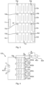
Figure 3 is a top view of aconductive layer 10 in a busbar according an embodiment of the present invention. Theconductive layer 10 has a machinedpattern 13 defining four parallel conductive paths as well asconnection sites connection sites input area 11, which is common to all four paths, each path passes through acommon portion 14 followed by a respective meandering portion that ends in a respective one of the fouroutput areas 12. For this purpose, the machinedpattern 13 not only comprises slots (vertically oriented infigure 3 ) in baffle-like arrangements but also slots (horizontally oriented infigure 3 ) which delimit one meandering portion of a conductive path from an adjacent one. Thecommon portion 14 may be said to be substantially straight in the sense that it allows current to flow substantially along a straight line connecting theinput area 11 and the beginning of the meandering portion of each conductive path. Each conductive path comprises an upstream 15 and a downstream 16 connection site, respectively located at the beginning and end of the meandering portion. The voltage drop over the meandering portion can be determined by electrically connecting the poles of a voltmeter or equivalent circuitry between theconnection sites figure 4 . - As exemplified by
figure 3 , the section of the conductive path joining the twoconnection sites connection sites -
Figure 4 is a top view of aconductive layer 10 belonging to a two-layer busbar according a further embodiment of the present invention. Theconductive layer 10 has a machinedpattern 13 which defines four parallel conductive paths. For illustration purposes,figure 4 shows acapacitor 401 having its two poles connected to theinput area 11 of the shownconductive layer 10 and to aninput area 21 of a second conductive layer (not shown) of the busbar. The twoinput areas capacitor 401 serving as a direct-current capacitor for intermediate storage of electric energy that may be supplied via conductors and/or for smoothing purposes.Figure 4 further shows four semiconductor devices 402, which are connected between arespective output area 12 of the shownconductive layer 10 and anoutput area 22 of the second conductive layer (not shown). Accordingly, between the poles of thecapacitor 401, there are four closed electric circuits, including a first circuit composed of: theinput area 11 in the first conductive layer 10 - the straight portion of the first conductive path - the meandering portion of the first conductive path - thefirst output area 12a of the first conductive layer 10 - thefirst semiconductor device 402a, thefirst output area 22a of the second conductive layer (not shown) - a conductive path of the second conductive layer (not shown) - theinput area 21 of the second conductive layer (not shown). - Unlike the conductive layer shown in
figure 3 , theconductive layer 10 illustrated infigure 4 comprises a singlededicated connection site 15 for each conductive path, namely, the upstream connection site. Therespective output areas 12 are used additionally as downstream conductive site, that is, for connecting one pole of the measurement equipment. In other words, the downstream conductive site coincides with theoutput area 12.Figure 4 further shows a first example current monitoring arrangement comprising resistors Rin , Rf and anoperational amplifier 403 configured to perform non-inverting amplification of the voltage drop between the firstupstream connection site 15a and thefirst output area 12a. A theoretical gain factor may be equal to 1 + Rf /Rin . The current monitoring arrangement further comprises asensor 404 for reading the amplified output of theoperational amplifier 403. Clearly, similar current monitoring arrangements may be provided at the second, third and fourth conductive paths on the firstconductive layer 10. - The current monitoring arrangements may be used to monitor derived electric quantities as well. In particular, the value of a capacitor connected to the
busbar 100, such as thecapacitor 401, may be monitored on the basis of the measured current. - The inventors furthermore envisage a second example current monitoring arrangement, which may replace the first example current monitoring arrangement but otherwise be connected in the same manner, to the
upstream connection site 15 and theoutput area 12. On a general functional level, the second example current monitoring arrangement is configured to separate low-frequency and high-frequency components of the measured voltage drop into separate branches of circuitry. This may be achieved by letting measurements on the low-frequency components primarily rely on the resistive properties of theconductive layer 10, whereas measurements on the high-frequency components may be based on inductive phenomena. The two signals picked up in this manner may undergo low-pass and high-pass filtering, respectively, and optional gain calibration before they are summed together, to form a complete frequency representation of the voltage drop signal. The second example current monitoring arrangement may be more sophisticated to implement but may provide greater accuracy and a more even output over the studied frequency range. -
Figure 5 illustrates, in accordance with a further embodiment, amachined pattern 13 on aconductive layer 10 of a busbar for providing a meandering conductive path. Themachined pattern 13, which comprises three vertical slots, defines a conductive path with two segments where the current is conveyed in a direction differing from an imaginary straight line between theinput area 11 andoutput area 12. - In accordance with a still further embodiment,
figure 6 shows aconductive layer 10 with amachined pattern 13 having a mere two vertical slots. The slots of the machinedpattern 13 define a conductive path that is not only slightly longer than an imaginary straight line between theinput area 11 andoutput area 12, but also significantly narrower in its central segment.Connection sites - Finally,
figure 7 shows amachined pattern 13 on aconductive layer 10 of a busbar for providing a meandering conductive path that includes at least one retrograde segment. More precisely, the conductive path between theinput area 11 and theoutput area 12 comprises a meandering portion which begins at theupstream connection site 15 and ends at thedownstream connection site 16. Between thesesites figure 7 , i.e., one where the flowing current approaches theinput area 11 again. The first segment is follows by a second segment, in which the current flows in an approximate south-southeast direction, and a third segment that is vertically oriented. The conductive pattern continues through on the right-hand half of theconductive pattern 13, where a vertical fourth segment is follows by a north-northeast fifth segment, a southeast sixth segment. In the sixth segment, again, current will be forced geometrically closer to theinput area 11 and away from theoutput area 12, that is, away from the general direction of travel. For this reason, the first and sixth segments may be referred to as retrograde segments. Machined patterns which define one or more retrograde segments are advantageous since theconnection sites - In one example, a busbar according to any of the described embodiments has a nominal current of at least 10 A, such as at least 100 A. The resistance of the busbar may range from 20 to 20 000 µΩ, such as 250 to 20 000 µΩ, or preferably 50 to 500 µΩ. In cases where multiple parallel conductive paths are provided, the resistance values apply for one conductive path.
- In another example, the busbar has a nominal current of at least 400 A and a resistance of 1 to 500 µΩ, preferably 10 to 100 µΩ, for one conductive path. Even for the highest resistance values, the losses due to current monitoring is of the order of tens of watts.
- By way of quantitative comparison in an example case, the resistance and inductance of a conductive busbar layer without and with a
machined pattern 13 of the type shown infigures 3 and 4 have been simulated by finite-element modeling using Ansys™ software. The simulation parameters and results are summarized in Table 1.Table 1: Simulation of busbar layers Without pattern With pattern Inter-layer distance (d) 300 µm 300 µm Width of pattern - 1 mm Total inductance 0.3 nH 2.1 nH Total resistance 3.7 µΩ 22.5 µΩ Resistance per parallel conductive path - 90 µΩ Simulation frequency 50 Hz 50 Hz - The aspects of the present disclosure have mainly been described above with reference to a few embodiments and examples thereof. However, as is readily appreciated by a person skilled in the art, other embodiments than the ones disclosed above are equally possible within the scope of the invention, as defined by the appended patent claims.
Claims (17)
- Power electronics circuitry, comprising:a busbar (100) comprising a first conductive layer (10) with an input area (11) and an output area (12),wherein the conductive layer has a machined pattern (13) defining a meandering conductive path between the input area and the output area; andwherein the power electronics circuitry further comprises: a current monitoring arrangement (403,404) adapted to sense a voltage drop over said meandering conductive path; the power electronics circuitry being characterised by a direct-current capacitor (401) connected at the input area of the busbar;a semiconductor device (402) connected at the output area of the busbar.
- The power electronics circuitry of claim 1, wherein the conductive path is at least 110%, preferably at least 125%, preferably at least 150%, preferably at least 2 or 5 or 10 times as long as the distance from the input area to the output area.
- The power electronics circuitry of any of the preceding claims, wherein the provision of the machined pattern increases the resistance between the input area and the output area by a factor greater than or equal to a concomitant inductance increase.
- The power electronics circuitry of any of the preceding claims, for which any of the following holds:a) the busbar has a nominal current of at least 10 A and a resistance of 20 to 20 000 µΩ, preferably 50 to 500 µΩ, for one conductive path;b) the busbar has a nominal current of at least 400 A and a resistance of 1 to 500 µΩ, preferably 10 to 100 µΩ, for one conductive path.
- The power electronics circuitry of any of the preceding claims, wherein the conductive path includes parallel adjacent opposite sections.
- The power electronics circuitry of any of the preceding claims, wherein a width of the machined pattern is at most 3 mm, preferably at most 2 mm, preferably at most 1 mm.
- The power electronics circuitry of any of the preceding claims, wherein the conductive layer has plural output areas (12a, 12b, 12c, 12d) and the machined pattern defines a meandering conductive path from the input area to a respective one of the output areas.
- The power electronics circuitry of claim 7, wherein the plural meandering conductive paths share a common portion (14) proximate to the input area.
- The power electronics circuitry of claim 8, wherein the common portion is substantially straight.
- The power electronics circuitry of any of the preceding claims, wherein the machined pattern is a chemically or photochemically machined pattern, preferably an etched pattern, a laser-cut pattern or a waterjet-cut pattern.
- The power electronics circuitry of any of the preceding claims, wherein the machined pattern is cut through the first conductive layer.
- The power electronics circuitry of any of the preceding claims, further comprising connection sites (15, 16) allowing to sense a voltage drop over the conductive path.
- The power electronics circuitry of claim 12, wherein one of the connection sites coincides with the output area.
- The power electronics circuitry of claim 12 or 13, wherein a section of the conductive path joining two connection sites (15, 16) is at least 2 times, preferably 5 times, preferably 10 times as long as the distance between the connection sites.
- The power electronics circuitry of claim 14, wherein said section includes at least one retrograde segment.
- The power electronics circuitry of any of the preceding claims, further comprising a parallel second conductive layer (20), which is separated from the first conductive layer and comprises a second input area (21) and second output area (22).
- The power electronics circuitry of claim 16, wherein the first and second conductive layers are separated by a void and/or by an insulating layer.
Applications Claiming Priority (1)
| Application Number | Priority Date | Filing Date | Title |
|---|---|---|---|
| PCT/EP2020/057895 WO2021185463A1 (en) | 2020-03-20 | 2020-03-20 | High-power busbar with controllable resistance |
Publications (2)
| Publication Number | Publication Date |
|---|---|
| EP4121783A1 EP4121783A1 (en) | 2023-01-25 |
| EP4121783B1 true EP4121783B1 (en) | 2025-05-07 |
Family
ID=70057081
Family Applications (1)
| Application Number | Title | Priority Date | Filing Date |
|---|---|---|---|
| EP20715288.5A Active EP4121783B1 (en) | 2020-03-20 | 2020-03-20 | Power electronics circuitry having high-power busbar with controllable resistance |
Country Status (2)
| Country | Link |
|---|---|
| EP (1) | EP4121783B1 (en) |
| WO (1) | WO2021185463A1 (en) |
Family Cites Families (5)
| Publication number | Priority date | Publication date | Assignee | Title |
|---|---|---|---|---|
| US5300917A (en) * | 1993-01-15 | 1994-04-05 | Maue H Winston | Junction box having integrally formed shunt |
| DE19542162C2 (en) * | 1995-11-11 | 2000-11-23 | Abb Research Ltd | Overcurrent limiter |
| DE102004042719A1 (en) * | 2004-09-03 | 2005-09-29 | Audi Ag | Current sensor has measurement resistance made as narrower length or meander integrated in same material as conductor |
| US8063845B2 (en) * | 2007-09-12 | 2011-11-22 | Flextronics Automotive Inc. | Symmetrical printed meander dipole antenna |
| EP2308088A1 (en) * | 2008-07-02 | 2011-04-13 | Nxp B.V. | Improved meander resistor |
-
2020
- 2020-03-20 WO PCT/EP2020/057895 patent/WO2021185463A1/en not_active Ceased
- 2020-03-20 EP EP20715288.5A patent/EP4121783B1/en active Active
Also Published As
| Publication number | Publication date |
|---|---|
| EP4121783A1 (en) | 2023-01-25 |
| WO2021185463A1 (en) | 2021-09-23 |
Similar Documents
| Publication | Publication Date | Title |
|---|---|---|
| JP4220094B2 (en) | Power semiconductor module | |
| US9410990B2 (en) | Method and sensor for sensing current in a conductor | |
| US7728578B2 (en) | Method and apparatus for high current measurement | |
| US11531075B2 (en) | Method and apparatus for integrating current sensors in a power semiconductor module | |
| US6271655B1 (en) | Planar coil device, method and system for sensing changing currents in a planar conductor path | |
| EP2570816B1 (en) | Apparatus and method for improved current shunt sensing | |
| US6677850B2 (en) | Layered current sensor | |
| US8228649B2 (en) | Impedance-based current sensor | |
| KR101981640B1 (en) | Current sensor for measuring alternative electromegnetic wave and current breker using the same | |
| SE512699C2 (en) | An inductance device | |
| JP4481369B2 (en) | AC current sensor | |
| CN109564249A (en) | Current Sense Amplifier Architecture and Level Shifter | |
| CN111065931A (en) | Current measuring device | |
| WO2017002766A1 (en) | Current detection device | |
| JP4853807B2 (en) | Current sensing device | |
| JPH08505941A (en) | Junction box with integrated shunt | |
| CN116868065A (en) | Current sensing device | |
| DE102015219364A1 (en) | Strornsensor | |
| EP2905626B1 (en) | Integrated current sensor system and method for producing an integrated current sensor system | |
| WO2021185463A1 (en) | High-power busbar with controllable resistance | |
| KR20250141090A (en) | Current Sensor with Core and Method of Manufacturing Thereof | |
| Wang et al. | Rogowski current sensor design and analysis based on printed circuit boards (PCB) | |
| CN109613321B (en) | Current measuring method and device for copper bar type lead | |
| US6567254B2 (en) | Methods and systems for reducing clamp voltages in surge protection circuitry | |
| US11092623B2 (en) | Current sensor for measuring alternating electromagnetic wave and a current breaker using the same |
Legal Events
| Date | Code | Title | Description |
|---|---|---|---|
| STAA | Information on the status of an ep patent application or granted ep patent |
Free format text: STATUS: UNKNOWN |
|
| STAA | Information on the status of an ep patent application or granted ep patent |
Free format text: STATUS: THE INTERNATIONAL PUBLICATION HAS BEEN MADE |
|
| PUAI | Public reference made under article 153(3) epc to a published international application that has entered the european phase |
Free format text: ORIGINAL CODE: 0009012 |
|
| STAA | Information on the status of an ep patent application or granted ep patent |
Free format text: STATUS: REQUEST FOR EXAMINATION WAS MADE |
|
| 17P | Request for examination filed |
Effective date: 20221006 |
|
| AK | Designated contracting states |
Kind code of ref document: A1 Designated state(s): AL AT BE BG CH CY CZ DE DK EE ES FI FR GB GR HR HU IE IS IT LI LT LU LV MC MK MT NL NO PL PT RO RS SE SI SK SM TR |
|
| DAV | Request for validation of the european patent (deleted) | ||
| DAX | Request for extension of the european patent (deleted) | ||
| GRAP | Despatch of communication of intention to grant a patent |
Free format text: ORIGINAL CODE: EPIDOSNIGR1 |
|
| STAA | Information on the status of an ep patent application or granted ep patent |
Free format text: STATUS: GRANT OF PATENT IS INTENDED |
|
| INTG | Intention to grant announced |
Effective date: 20241108 |
|
| GRAS | Grant fee paid |
Free format text: ORIGINAL CODE: EPIDOSNIGR3 |
|
| GRAA | (expected) grant |
Free format text: ORIGINAL CODE: 0009210 |
|
| STAA | Information on the status of an ep patent application or granted ep patent |
Free format text: STATUS: THE PATENT HAS BEEN GRANTED |
|
| AK | Designated contracting states |
Kind code of ref document: B1 Designated state(s): AL AT BE BG CH CY CZ DE DK EE ES FI FR GB GR HR HU IE IS IT LI LT LU LV MC MK MT NL NO PL PT RO RS SE SI SK SM TR |
|
| REG | Reference to a national code |
Ref country code: GB Ref legal event code: FG4D |
|
| REG | Reference to a national code |
Ref country code: CH Ref legal event code: EP |
|
| REG | Reference to a national code |
Ref country code: DE Ref legal event code: R096 Ref document number: 602020050791 Country of ref document: DE |
|
| REG | Reference to a national code |
Ref country code: IE Ref legal event code: FG4D |
|
| REG | Reference to a national code |
Ref country code: NL Ref legal event code: MP Effective date: 20250507 |
|
| PG25 | Lapsed in a contracting state [announced via postgrant information from national office to epo] |
Ref country code: PT Free format text: LAPSE BECAUSE OF FAILURE TO SUBMIT A TRANSLATION OF THE DESCRIPTION OR TO PAY THE FEE WITHIN THE PRESCRIBED TIME-LIMIT Effective date: 20250908 Ref country code: FI Free format text: LAPSE BECAUSE OF FAILURE TO SUBMIT A TRANSLATION OF THE DESCRIPTION OR TO PAY THE FEE WITHIN THE PRESCRIBED TIME-LIMIT Effective date: 20250507 Ref country code: ES Free format text: LAPSE BECAUSE OF FAILURE TO SUBMIT A TRANSLATION OF THE DESCRIPTION OR TO PAY THE FEE WITHIN THE PRESCRIBED TIME-LIMIT Effective date: 20250507 |
|
| REG | Reference to a national code |
Ref country code: LT Ref legal event code: MG9D |
|
| PG25 | Lapsed in a contracting state [announced via postgrant information from national office to epo] |
Ref country code: NO Free format text: LAPSE BECAUSE OF FAILURE TO SUBMIT A TRANSLATION OF THE DESCRIPTION OR TO PAY THE FEE WITHIN THE PRESCRIBED TIME-LIMIT Effective date: 20250807 Ref country code: GR Free format text: LAPSE BECAUSE OF FAILURE TO SUBMIT A TRANSLATION OF THE DESCRIPTION OR TO PAY THE FEE WITHIN THE PRESCRIBED TIME-LIMIT Effective date: 20250808 |
|
| PG25 | Lapsed in a contracting state [announced via postgrant information from national office to epo] |
Ref country code: NL Free format text: LAPSE BECAUSE OF FAILURE TO SUBMIT A TRANSLATION OF THE DESCRIPTION OR TO PAY THE FEE WITHIN THE PRESCRIBED TIME-LIMIT Effective date: 20250507 Ref country code: PL Free format text: LAPSE BECAUSE OF FAILURE TO SUBMIT A TRANSLATION OF THE DESCRIPTION OR TO PAY THE FEE WITHIN THE PRESCRIBED TIME-LIMIT Effective date: 20250507 |
|
| REG | Reference to a national code |
Ref country code: AT Ref legal event code: MK05 Ref document number: 1793003 Country of ref document: AT Kind code of ref document: T Effective date: 20250507 |
|
| PG25 | Lapsed in a contracting state [announced via postgrant information from national office to epo] |
Ref country code: BG Free format text: LAPSE BECAUSE OF FAILURE TO SUBMIT A TRANSLATION OF THE DESCRIPTION OR TO PAY THE FEE WITHIN THE PRESCRIBED TIME-LIMIT Effective date: 20250507 |
|
| PG25 | Lapsed in a contracting state [announced via postgrant information from national office to epo] |
Ref country code: HR Free format text: LAPSE BECAUSE OF FAILURE TO SUBMIT A TRANSLATION OF THE DESCRIPTION OR TO PAY THE FEE WITHIN THE PRESCRIBED TIME-LIMIT Effective date: 20250507 |
|
| PG25 | Lapsed in a contracting state [announced via postgrant information from national office to epo] |
Ref country code: AT Free format text: LAPSE BECAUSE OF FAILURE TO SUBMIT A TRANSLATION OF THE DESCRIPTION OR TO PAY THE FEE WITHIN THE PRESCRIBED TIME-LIMIT Effective date: 20250507 |
|
| PG25 | Lapsed in a contracting state [announced via postgrant information from national office to epo] |
Ref country code: RS Free format text: LAPSE BECAUSE OF FAILURE TO SUBMIT A TRANSLATION OF THE DESCRIPTION OR TO PAY THE FEE WITHIN THE PRESCRIBED TIME-LIMIT Effective date: 20250807 |
|
| PG25 | Lapsed in a contracting state [announced via postgrant information from national office to epo] |
Ref country code: IS Free format text: LAPSE BECAUSE OF FAILURE TO SUBMIT A TRANSLATION OF THE DESCRIPTION OR TO PAY THE FEE WITHIN THE PRESCRIBED TIME-LIMIT Effective date: 20250907 |
|
| PG25 | Lapsed in a contracting state [announced via postgrant information from national office to epo] |
Ref country code: LV Free format text: LAPSE BECAUSE OF FAILURE TO SUBMIT A TRANSLATION OF THE DESCRIPTION OR TO PAY THE FEE WITHIN THE PRESCRIBED TIME-LIMIT Effective date: 20250507 |
|
| PG25 | Lapsed in a contracting state [announced via postgrant information from national office to epo] |
Ref country code: DK Free format text: LAPSE BECAUSE OF FAILURE TO SUBMIT A TRANSLATION OF THE DESCRIPTION OR TO PAY THE FEE WITHIN THE PRESCRIBED TIME-LIMIT Effective date: 20250507 Ref country code: SM Free format text: LAPSE BECAUSE OF FAILURE TO SUBMIT A TRANSLATION OF THE DESCRIPTION OR TO PAY THE FEE WITHIN THE PRESCRIBED TIME-LIMIT Effective date: 20250507 |
|
| PG25 | Lapsed in a contracting state [announced via postgrant information from national office to epo] |
Ref country code: CZ Free format text: LAPSE BECAUSE OF FAILURE TO SUBMIT A TRANSLATION OF THE DESCRIPTION OR TO PAY THE FEE WITHIN THE PRESCRIBED TIME-LIMIT Effective date: 20250507 |
|
| PG25 | Lapsed in a contracting state [announced via postgrant information from national office to epo] |
Ref country code: EE Free format text: LAPSE BECAUSE OF FAILURE TO SUBMIT A TRANSLATION OF THE DESCRIPTION OR TO PAY THE FEE WITHIN THE PRESCRIBED TIME-LIMIT Effective date: 20250507 |
|
| PG25 | Lapsed in a contracting state [announced via postgrant information from national office to epo] |
Ref country code: SK Free format text: LAPSE BECAUSE OF FAILURE TO SUBMIT A TRANSLATION OF THE DESCRIPTION OR TO PAY THE FEE WITHIN THE PRESCRIBED TIME-LIMIT Effective date: 20250507 |
|
| PG25 | Lapsed in a contracting state [announced via postgrant information from national office to epo] |
Ref country code: IT Free format text: LAPSE BECAUSE OF FAILURE TO SUBMIT A TRANSLATION OF THE DESCRIPTION OR TO PAY THE FEE WITHIN THE PRESCRIBED TIME-LIMIT Effective date: 20250507 |
|
| REG | Reference to a national code |
Ref country code: DE Ref legal event code: R097 Ref document number: 602020050791 Country of ref document: DE |
|
| PLBE | No opposition filed within time limit |
Free format text: ORIGINAL CODE: 0009261 |
|
| STAA | Information on the status of an ep patent application or granted ep patent |
Free format text: STATUS: NO OPPOSITION FILED WITHIN TIME LIMIT |
|
| REG | Reference to a national code |
Ref country code: CH Ref legal event code: L10 Free format text: ST27 STATUS EVENT CODE: U-0-0-L10-L00 (AS PROVIDED BY THE NATIONAL OFFICE) Effective date: 20260318 |
|
| 26N | No opposition filed |
Effective date: 20260210 |
|
| PGFP | Annual fee paid to national office [announced via postgrant information from national office to epo] |
Ref country code: FR Payment date: 20260323 Year of fee payment: 7 |