EP4120510A1 - Wireless power reception device and wireless power transmission device - Google Patents
Wireless power reception device and wireless power transmission device Download PDFInfo
- Publication number
- EP4120510A1 EP4120510A1 EP21862122.5A EP21862122A EP4120510A1 EP 4120510 A1 EP4120510 A1 EP 4120510A1 EP 21862122 A EP21862122 A EP 21862122A EP 4120510 A1 EP4120510 A1 EP 4120510A1
- Authority
- EP
- European Patent Office
- Prior art keywords
- less
- inductance
- side resonant
- wireless power
- transmitting
- Prior art date
- Legal status (The legal status is an assumption and is not a legal conclusion. Google has not performed a legal analysis and makes no representation as to the accuracy of the status listed.)
- Pending
Links
Images





Classifications
-
- H—ELECTRICITY
- H02—GENERATION; CONVERSION OR DISTRIBUTION OF ELECTRIC POWER
- H02J—ELECTRIC POWER NETWORKS; CIRCUIT ARRANGEMENTS OR SYSTEMS FOR SUPPLYING OR DISTRIBUTING ELECTRIC POWER; SYSTEMS FOR STORING ELECTRIC ENERGY
- H02J50/00—Circuit arrangements or systems for wireless supply or distribution of electric power
- H02J50/10—Circuit arrangements or systems for wireless supply or distribution of electric power using inductive coupling
- H02J50/12—Circuit arrangements or systems for wireless supply or distribution of electric power using inductive coupling of the resonant type
-
- H—ELECTRICITY
- H01—ELECTRIC ELEMENTS
- H01F—MAGNETS; INDUCTANCES; TRANSFORMERS; SELECTION OF MATERIALS FOR THEIR MAGNETIC PROPERTIES
- H01F27/00—Details of transformers or inductances, in general
- H01F27/24—Magnetic cores
- H01F27/255—Magnetic cores made from particles
-
- H—ELECTRICITY
- H01—ELECTRIC ELEMENTS
- H01F—MAGNETS; INDUCTANCES; TRANSFORMERS; SELECTION OF MATERIALS FOR THEIR MAGNETIC PROPERTIES
- H01F27/00—Details of transformers or inductances, in general
- H01F27/34—Special means for preventing or reducing unwanted electric or magnetic effects, e.g. no-load losses, reactive currents, harmonics, oscillations, leakage fields
-
- H—ELECTRICITY
- H01—ELECTRIC ELEMENTS
- H01F—MAGNETS; INDUCTANCES; TRANSFORMERS; SELECTION OF MATERIALS FOR THEIR MAGNETIC PROPERTIES
- H01F38/00—Adaptations of transformers or inductances for specific applications or functions
- H01F38/14—Inductive couplings
-
- H—ELECTRICITY
- H02—GENERATION; CONVERSION OR DISTRIBUTION OF ELECTRIC POWER
- H02J—ELECTRIC POWER NETWORKS; CIRCUIT ARRANGEMENTS OR SYSTEMS FOR SUPPLYING OR DISTRIBUTING ELECTRIC POWER; SYSTEMS FOR STORING ELECTRIC ENERGY
- H02J50/00—Circuit arrangements or systems for wireless supply or distribution of electric power
- H02J50/005—Mechanical details of housing or structure aiming to accommodate the power transfer means, e.g. mechanical integration of coils, antennas or transducers into emitting or receiving devices
-
- H—ELECTRICITY
- H02—GENERATION; CONVERSION OR DISTRIBUTION OF ELECTRIC POWER
- H02J—ELECTRIC POWER NETWORKS; CIRCUIT ARRANGEMENTS OR SYSTEMS FOR SUPPLYING OR DISTRIBUTING ELECTRIC POWER; SYSTEMS FOR STORING ELECTRIC ENERGY
- H02J50/00—Circuit arrangements or systems for wireless supply or distribution of electric power
- H02J50/80—Circuit arrangements or systems for wireless supply or distribution of electric power involving the exchange of data, concerning supply or distribution of electric power, between transmitting devices and receiving devices
-
- H—ELECTRICITY
- H02—GENERATION; CONVERSION OR DISTRIBUTION OF ELECTRIC POWER
- H02M—APPARATUS FOR CONVERSION BETWEEN AC AND AC, BETWEEN AC AND DC, OR BETWEEN DC AND DC, AND FOR USE WITH MAINS OR SIMILAR POWER SUPPLY SYSTEMS; CONVERSION OF DC OR AC INPUT POWER INTO SURGE OUTPUT POWER; CONTROL OR REGULATION THEREOF
- H02M7/00—Conversion of AC power input into DC power output; Conversion of DC power input into AC power output
- H02M7/02—Conversion of AC power input into DC power output without possibility of reversal
- H02M7/04—Conversion of AC power input into DC power output without possibility of reversal by static converters
- H02M7/06—Conversion of AC power input into DC power output without possibility of reversal by static converters using discharge tubes without control electrode or semiconductor devices without control electrode
-
- H—ELECTRICITY
- H02—GENERATION; CONVERSION OR DISTRIBUTION OF ELECTRIC POWER
- H02M—APPARATUS FOR CONVERSION BETWEEN AC AND AC, BETWEEN AC AND DC, OR BETWEEN DC AND DC, AND FOR USE WITH MAINS OR SIMILAR POWER SUPPLY SYSTEMS; CONVERSION OF DC OR AC INPUT POWER INTO SURGE OUTPUT POWER; CONTROL OR REGULATION THEREOF
- H02M7/00—Conversion of AC power input into DC power output; Conversion of DC power input into AC power output
- H02M7/42—Conversion of DC power input into AC power output without possibility of reversal
- H02M7/44—Conversion of DC power input into AC power output without possibility of reversal by static converters
- H02M7/48—Conversion of DC power input into AC power output without possibility of reversal by static converters using discharge tubes with control electrode or semiconductor devices with control electrode
- H02M7/53—Conversion of DC power input into AC power output without possibility of reversal by static converters using discharge tubes with control electrode or semiconductor devices with control electrode using devices of a triode or transistor type requiring continuous application of a control signal
- H02M7/537—Conversion of DC power input into AC power output without possibility of reversal by static converters using discharge tubes with control electrode or semiconductor devices with control electrode using devices of a triode or transistor type requiring continuous application of a control signal using semiconductor devices only, e.g. single switched pulse inverters
- H02M7/5387—Conversion of DC power input into AC power output without possibility of reversal by static converters using discharge tubes with control electrode or semiconductor devices with control electrode using devices of a triode or transistor type requiring continuous application of a control signal using semiconductor devices only, e.g. single switched pulse inverters in a bridge configuration
-
- Y—GENERAL TAGGING OF NEW TECHNOLOGICAL DEVELOPMENTS; GENERAL TAGGING OF CROSS-SECTIONAL TECHNOLOGIES SPANNING OVER SEVERAL SECTIONS OF THE IPC; TECHNICAL SUBJECTS COVERED BY FORMER USPC CROSS-REFERENCE ART COLLECTIONS [XRACs] AND DIGESTS
- Y02—TECHNOLOGIES OR APPLICATIONS FOR MITIGATION OR ADAPTATION AGAINST CLIMATE CHANGE
- Y02B—CLIMATE CHANGE MITIGATION TECHNOLOGIES RELATED TO BUILDINGS, e.g. HOUSING, HOUSE APPLIANCES OR RELATED END-USER APPLICATIONS
- Y02B70/00—Technologies for an efficient end-user side electric power management and consumption
- Y02B70/10—Technologies improving the efficiency by using switched-mode power supplies [SMPS], i.e. efficient power electronics conversion e.g. power factor correction or reduction of losses in power supplies or efficient standby modes
Definitions
- Embodiments of the present disclosure relates to a wireless power receiver and wireless power transmitter which receive and transmit wireless power.
- wireless power transmission refers to a technology for supplying power to a means of transport using wireless electricity without a conventional wired power line.
- Various types of wireless power transmission are being developed due to advantages such as offering more user convenience in the use of electricity, reducing the risk of electrical shock, and enhancing aesthetical appearance.
- Conventional wireless power transceivers are configured by designing parameters for a resonant network, and their output power is determined by using the same configuration on a transmitting side resonant inductor and a receiving side resonant inductor.
- Magnetic materials are being used as the material of pads in recent years, in order to uniformly distribute a magnetic flux generated by transmitting/receiving pads used in wireless power transceivers.
- some of these magnetic materials are hard to apply in real-life settings where the inside of a space is enclosed, due to their low permeability and relatively high heat generation.
- embodiments of the present disclosure provides a wireless power receiver and a wireless power transmitter for reducing heat generated by pads used in the wireless power transceiver.
- a wireless power receiver includes: a receiving pad configured to receive power transmitted from a wireless power transmitter including a transmitting pad and a transmitting side resonant inductor; and a receiving side resonant network including a receiving side resonant inductor that controls power supplied to the receiving pad, and a first inductance of the receiving side resonant inductor and a second inductance of the transmitting side resonant inductor are determined to be different from each other.
- the first inductance of the receiving side resonant inductor may be determined to be lower than the second inductance of the transmitting side resonant inductor.
- the ratio of the first inductance to the second inductance may be determined to be less than 1.
- a heat generation temperature variation rate measured during 30 minutes from the time the power is received from the wireless power transmitter may be less than or equal to 2.0.
- a heat generation temperature variation rate measured during 10 minutes from the time the power is received from the wireless power transmitter may be less than or equal to 3.1.
- a wireless power transmitter includes: a transmitting pad configured to transmit power to a wireless power receiver including a receiving pad and a receiving side resonant inductor; and a transmitting side resonant network including a transmitting side resonant inductor that controls power supplied to the transmitting pad, and a first inductance of the receiving side resonant inductor and a second inductance of the transmitting side resonant inductor are determined to be different from each other.
- first inductance of the receiving side resonant inductor may be determined to be lower than the second inductance of the transmitting side resonant inductor, and the ratio of the first inductance to the second inductance may be determined to be less than 1.
- a heat generation temperature variation rate measured during 30 minutes from the time the power is transmitted to the wireless power receiver may be less than or equal to 2.0.
- a heat generation temperature variation rate measured during 20 minutes from the time the power is transmitted to the wireless power receiver may be less than or equal to 2.4.
- a heat generation temperature variation rate measured during 10 minutes from the time the power may be transmitted to the wireless power receiver is less than or equal to 3.1.
- a heat generation temperature variation rate measured during 30 minutes from the time the power is transmitted to the wireless power receiver may be less than or equal to 3.00.
- a heat generation temperature variation rate measured during 20 minutes from the time the power is transmitted to the wireless power receiver may be less than or equal to 3.8.
- a means of transport includes: a wireless power receiver including a receiving pad configured to receive power transmitted from a wireless power transmitter having a transmitting pad and a transmitting side resonant inductor, and a receiving side resonant network having a receiving side resonant inductor that controls power supplied to the receiving pad; and a battery that is charged with power received by using the wireless power receiver, and a first inductance of the receiving side resonant inductor and a second inductance of the transmitting side resonant inductor are determined to be different from each other.
- FIG. 1 is a block diagram showing a wireless power transceiver according to an embodiment of the present disclosure.
- FIG. 2 is a circuit diagram of the wireless power transceiver of FIG. 1 .
- the wireless power transceiver 1000 may include a wireless power transmitter 100 and a wireless power receiver 200.
- the wireless power transmitter 100 may include a voltage converter 110, a transmitting side resonant network 120, and a transmitting pad 130.
- the voltage converter 110 may convert a first input voltage U DC of DC into an AC voltage.
- the voltage converter 110 may include a plurality of rectifiers Q 1 , Q 2 , Q 3 , and Q 4 , and each of the rectifiers Q 1 , Q 2 , Q 3 , and Q 4 may include an inverter (e.g., MOSFET) and a converter (e.g., diode).
- an inverter e.g., MOSFET
- a converter e.g., diode
- the connections between the rectifiers Q 1 , Q 2 , Q 3 , and Q 4 included in the voltage converter 110 are as follows.
- a positive terminal of the first input voltage U DC , one end (e.g., drain of MOSFET) of the first rectifier Q 1 , and one end (e.g., drain of MOSFET) of the third rectifier Q 3 may be connected to a fourth node D, and the other end (e.g., source of MOSFET) of the first rectifier Q 1 and one end (e.g., drain of MOSFET) of the second rectifier Q 2 may be connected to a first node A.
- one end (e.g., drain of MOSFET) of the fourth rectifier Q 4 and the other end (e.g., source of MOSFET) of the third rectifier Q 3 may be connected to a second node B, and the other end (e.g., source of MOSFET) of the second rectifier Q 2 and the other end (e.g., source of MOSFET) of the fourth rectifier Q4 may be connected to a third node C.
- the transmitting side resonant network 120 may include a transmitting side resonant inductor L 1 , a first transmitting side resonant capacitor C f1 , and a second transmitting side resonant capacitor C p1 .
- the connections between impedances included in the transmitting side resonant network 120 are as follows. One end of the transmitting side resonant inductor L 1 , one end of the first transmitting side resonant capacitor C f1 , and one end of the second transmitting side resonant capacitor C p1 may be connected to a fifth node E, the other end of the second transmitting side resonant capacitor C p1 may be connected to the second node B, and the other end of the transmitting side resonant inductor L 1 may be connected to the first node A.
- the transmitting pad 130 may be made of a magnet or a magnetic composite.
- the magnet may have a permeability greater than 300 H/m
- the magnetic composite may have a permeability of 300 H/m or less.
- the polymer magnetic composite may have less defects over a wide area and receive less damage from impacts as the fillers are held together by the binder resin.
- the fillers may be oxide fillers such as ferrites (Ni-Zn, Mg-Zn, and Mn-Zn ferrites); metallic fillers such as permalloy, sendust, and nanocrystalline magnetic material; or a powder mixture thereof. More specifically, the fillers may be sendust particles with an alloy composition of Fe-Si-Al.
- the fillers may have a composition with the following Chemical Formula 1: ⁇ Chemical Formula 1> Fe1-a-b-c Sia Xb Yc where X may be Al, Cr, Ni, Cu, or a combination thereof; Y may be Mn, B, Co, Mo, or a combination thereof; and 0.01 ⁇ a ⁇ 0.2, 0.01 ⁇ b ⁇ 0.1, and 0 ⁇ c ⁇ 0.05.
- X may be Al, Cr, or a combination thereof.
- the fillers may include sendust.
- the average particle diameter D50 of the fillers may range from around 1 ⁇ m to 300 ⁇ m, from around 10 ⁇ m to 200 ⁇ m, or from around 30 ⁇ m to 150 ⁇ m. If the average particle diameter of the fillers meets the above range, the rate of change of position at temperatures from 150 °C to 180 °C may be made as low as possible, thereby further improving the heat resistance properties and magnetic properties of the magnetic composite and therefore leading to better charging efficiency.
- the fillers may make up 60 %, 70%, or 85 % by weight or more of the total weight of the polymer magnetic composite.
- the filler content of the polymer magnetic composite may range from 60 % to 90 % by weight, from 70 % to 90 % by weight, from 75 % to 90 % by weight, from 78 % to 90 % by weight, from 80 % to 90 % by weight, from 85 % to 90 % by weight, from 87 % to 90 % by weight, or from 89 % to 90 % by weight. If the filler content is less than 60 % by weight, the rate of change of the position of the polymer magnetic composite increases and therefore the heat resistance properties of the magnetic composite degrade, which may cause deformation of and damage to the magnetic composite at high temperatures and weaken its magnetic properties and lower its charging efficiency.
- the melting point Tm of the binder resin may range from 150 °C to 210 °C.
- the melting point Tm of the binder resin may range from 160 °C to 200 °C, e.g., from 160 °C to 180 °C. If the melting point Tm of the binder resin meets the above range, the rate of change of position at temperatures of 150 °C to 180 °C may be made as low as possible, thereby further improving the heat resistance properties and magnetic properties of the magnetic composite and therefore leading to better charging efficiency.
- the binder resin may include one or more selected from the group consisting of polyimide resin, polyamide resin, polyamide-imide resin, polycarbonate resin, acrylonitrile butadiene styrene (ABS) resin, polypropylene resin, polyethylene resin, polystyrene resin, polyphenylene sulfide (PPS) resin, polyether ether ketone (PEEK) resin, silicone resin, acrylic resin, polyurethane resin, polyester resin, isocyanate resin, and epoxy resin.
- ABS acrylonitrile butadiene styrene
- PPS polyphenylene sulfide
- PEEK polyether ether ketone
- the binder resin may be a curable resin.
- the binder resin may be a photocurable resin and/or a thermosetting resin, especially a resin that can be cured and adhesive.
- the binder resin may be a resin containing one or more thermally curable functional groups or sites such as a glycidyl group, an isocyanate group, a hydroxy group, a carboxyl group, or an amide group; or one or more functional groups or sites that are curable by an activated energy, such as an epoxide group, a cyclic ether group, a sulfide group, an acetal group, or a lactone group. Examples of these functional groups or sites may include an isocyanate group (-NCO), a hydroxy group (-OH), or a carboxyl group (-COOH).
- the binder resin may include one or more selected from the group consisting of polyamide resin, polycarbonate resin, and polypropylene resin.
- the binder resin may increase the rate of change of position at temperatures of 150 °C to 180 °C unless it mixes well with the fillers. Accordingly, it may be important to choose the material of the binder resin that mixes well with the fillers.
- the binder resin content of the polymer magnetic composite may range from 5 % to 40 % by weight, from 10 % to 40 % by weight, from 10 % to 20 % by weight, from 5 % to 20 % by weight, from 5 % to 15 % by weight, or from 7 % to 15 % by weight.
- the binder resin content may range from 10 % to 40 % by weight, and the filler content may range 60 % to 90 % by weight, in order that the rate of change of the position of the polymer magnetic composite is controlled to be 20 % or less at temperatures of 150 °C to 180 °C.
- the binder resin content may range from 10 % to 20 % by weight, and the filler content may range from 80 % to 90 % by weight, in order that the rate of change of the position of the polymer magnetic composite is controlled to be 3 % or less at temperatures of 150 °C to 180 °C.
- the polymer magnetic composite may further include an additive.
- the polymer magnetic composite may further include one or more insulating coating agents selected from the group consisting of phosphoric acid and silane.
- the additive and the insulating coating agent may range from 0.1 % to 10 % by weight of the total weight of the polymer magnetic composite.
- the additive content is within the above range, it is easier to reduce the rate of change of position at temperatures of 150 °C to 180 °C, thereby improving charging efficiency.
- the polymer magnetic composite may be elongated by a certain percentage.
- the polymer magnetic composite may have an elongation of 0.5 % or more. Elongation properties are hard to obtain from ceramic magnetic composites which do not use polymer, and help reduce damage to large-area magnetic components even if they are distorted by impact.
- the polymer magnetic composite may have an elongation of 0.5 % or more, 1 % or more, or 2.5 % or more. Although there is no upper limit for elongation, increasing the polymer resin content may degrade the physical properties of the magnetic composite, such as inductance, so it is desirable to keep the elongation at or below 10 %.
- the transmitting pad 130 may include a flat-sheet structure, a stepwise structure, or a sandwiched structured.
- the transmitting pad 130 may include a transmitting coil L P .
- the transmitting coil L P may transmit electrical energy to a receiving coil L S without physical contact between electrodes via a magnetic field.
- the wireless power receiver 200 may include a receiving pad 210, a receiving side resonant network 220, a rectifying section 230, and a load section 240.
- the receiving pad 210 may be made of a magnet or a magnetic composite.
- the magnet may have a permeability greater than 300 H/m, and the magnetic composite may have a permeability of 300 H/m or less.
- the magnet may include a ferrite, and the magnetic composite may include a polymer magnetic composite including a binder resin and fillers distributed in the binder resin.
- the polymer magnetic composite may include a polymer magnetic block PMB
- the types of magnet and magnetic composite are not limited to the above examples. A description of the polymer magnetic composite will be omitted since it will be redundant with the foregoing description of the transmitting pad 130.
- the receiving pad 210 may include a receiving coil L S .
- the receiving side resonant network 220 may be configured in the same manner as the transmitting side resonant network 120. That is, the receiving side resonant network 220 may include a receiving side resonant inductor L 2 , a first receiving side resonant capacitor C f2 , and a second receiving side resonant capacitor C p2 .
- one end of the first receiving side resonant capacitor C f2 and one end of the receiving side resonant inductor L 2 may be connected to a sixth node F.
- the other end of the receiving side resonant inductor L 2 may be connected to a seventh node G.
- one end of the second receiving side resonant capacitor C p2 may be connected to the sixth node F, and the other end of the second receiving side resonant capacitor C p2 may be connected to the seventh node H.
- the rectifying section 230 is a full bridge circuit with a plurality of diodes D 1 , D 2 , D 3 , and D 4 , which may rectify a voltage received from the receiving side resonant network 220 by the diodes D 1 , D 2 , D 3 , and D 4 and transmit it to the load section 240.
- One end of the first diode D 1 and one end of the third diode D 3 may be connected to an eighth node H, and the other end of the first diode D 1 and one end of the second diode D 2 may be connected to the seventh node G.
- the other end of the third diode D 3 and one end of the fourth diode D 4 may be connected to the ninth node I, and the other end of the second diode D 2 and the other end of the fourth diode D 4 may be connected to a tenth node J.
- the load section 240 is comprised of an output capacitor Co and a load resistor R L , in which case the load resistor R L may be a battery. Both ends of the output capacitor Co may be connected to upper and lower contact points of the full bridge circuit constituting the rectifying section 230 and receive a rectified output voltage through the rectifying section 230. For example, both ends of the output capacitor Co may be connected between the eight node H and the tenth node J.
- the inductance of the transmitting side resonant inductor L 1 of the transmitting side resonant network 120 and the inductance of the receiving side resonant inductor L 2 of the receiving side resonant network 220 may be set.
- the inductance of the transmitting side resonant inductor L 1 and the inductance of the receiving side resonant inductor L 2 may be set based on size and weight limitations of the transmitting and receiving coils.
- an output current I o of the receiving side resonant network 220 may be inversely proportional to the product of the inductance of the transmitting side resonant inductor L 1 and the inductance of the receiving side resonant inductor L 2 .
- a transmitting coil current I p of the transmitting side resonant network 120 may be inversely proportional the inductance of the transmitting side resonant inductor L 1 .
- a receiving coil current I s of the receiving pad 210 may be inversely proportional to the product of the inductance of the transmitting side resonant inductor L 1 and the square of the inductance of the receiving side resonant inductor L 2 . I s ⁇ 1 L 1 L 2 2
- the inductance of the transmitting side resonant inductor L 1 and the inductance of the receiving side resonant inductor L 2 may be regulated or changed to vary the transmitting coil current I p that is the current at the transmitting side and the receiving coil current I s that is the current at the receiving side.
- increasing the transmitting side resonant inductor L 1 and decreasing the receiving side resonant inductor L 2 may decrease the transmitting coil current I p and increase the receiving coil current I s .
- decreasing the transmitting side resonant inductor L 1 and increasing the receiving side resonant inductor L 2 may increase the transmitting coil current I p and decrease the receiving coil current I s .
- the inductance of the transmitting side resonant inductor L 1 may be defined as in equation 4.
- the CR current ratio
- L 1 CRL ′
- the transmitting coil current I p and the receiving coil current I s may be determined to be inversely proportional to each other.
- the heat generation of the receiving pad 210 may be reduced by decreasing the receiving coil current I s and increasing the transmitting coil current I p , thereby improving overall efficiency.
- the magnetic flux ⁇ p of the transmitting pad 130 may be determined by equation 7, and the magnetic flux ⁇ s of the receiving pad 210 may be determined by equation 8.
- ⁇ p I p L pk 1 + I LM L m N
- ⁇ s I s L sk 2 + I LM L m N
- L pk1 is the leakage inductance of the transmitting coil Lp
- L sk2 is the leakage inductance of the receiving coil L s
- L m is magnetizing inductance
- I LM magnetizing current.
- controlling the CR makes it possible to regulate magnetic flux distribution such that there is no magnetic flux locally generated in the transmitting and receiving pads 130 and 210, which enables more efficient control of the heat generation in the transmitting and receiving pads 130 and 210.
- FIG. 3 is a graph showing the change of the value of the receiving coil current I s and the value of transmitting coil current I p versus CR.
- FIG. 4 is a graph showing the change of the value of the transmitting coil magnetic flux and the value of receiving coil magnetic flux versus CR.
- the transmitting coil current I p is greater than the receiving coil current I s when the CR is less than or equal to approximately 1.1.
- the transmitting coil current I p is smaller than the receiving coil current I s when the CR is greater than approximately 1.1.
- the transmitting and receiving pads 130 and 210 are made using a magnetic material and the output power is 6.6 kW, but not limited thereto.
- the magnetic flux ⁇ p of the transmitting coil is greater than the magnetic flux ⁇ s of the receiving coil when the CR is less than or equal to approximately 0.9, and that the magnetic flux ⁇ p of the transmitting coil is smaller than the magnetic flux ⁇ s of the receiving coil when the CR is greater than approximately 0.9.
- the CR By setting the CR to be less than or equal to approximately 0.9, the current and magnetic flux of the receiving coil become smaller than the current and magnetic flux of the transmitting coil, which may reduce the heat generation in the receiving pad 210.
- the CR may be set to a value of 0.6 to 0.9.
- FIG. 5 is a view showing the variation of magnetic flux distribution in the transmitting and receiving pads versus CR.
- the receiving pad 210 has a lower magnetic flux density and a more uniform magnetic flux distribution over the entire area of the receiving pad 210, as compared to when the CR is 1, which results in less heat generation.
- the charging frequency was set to 85 kHz, and voltage and current were supplied using a power supply.
- E-Load which is used for performance diagnostic testing, was connected to a tip end of the wireless power receiver 200.
- the output power was set to 8.8 kW, and the charging efficiency and heat generation temperature of the receiving pad 210 were measured for an operation time of 30 minutes.
- the CR When there is a need to control the heat generation temperature of the receiving pad 130, the CR may be designed as CR ⁇ 1, and when there is a need to control the heat generation temperature of the transmitting pad 230 because the receiver 200 is easily cooled, the CR may be designed as CR ⁇ 1.
- the wireless power transmitter 100 may be installed at a charging station, and the wireless power receiver 200 may be installed at the means of transport.
- the means of transport may be limited in heat dissipation compared to the charging station due to size limitations, technical limitations, and so on, which calls for a method for reducing the heat generation in the means of transport.
- the inductance of the transmitting side resonant inductor L 1 included in the wireless power transmitter 100 and/or the inductance of the receiving side resonant inductor L 2 included in the wireless power receiver 200 may be regulated, and therefore the heat generation temperature of the receiving pad 130 may be reduced, which may lead to, but not limited to, a reduction in the heat generation in the means of transport. That is, the above description may apply equally to reducing the heat generation in the charging station, as well as to reducing the heat generation in the means of transport.
- the ratio (CR) of the inductance of the transmitting side resonant inductor L 1 to the inductance of the receiving side resonant inductor L 2 may be less than 1. Further, the ratio (CR) of the inductance of the transmitting side resonant inductor L 1 to the inductance of the receiving side resonant inductor L 2 may be greater than or equal to 0.6, 0.7, or 0.8.
- FIG. 6 is a table showing the charging efficiency and heat generation temperature over time at different CR values when the receiving pad has a magnetic permeability greater than 300.
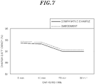
- FIG. 7 is a graph showing the variation of the charging efficiency over time at different CR values when the receiving pad has a magnetic permeability greater than 300.
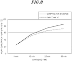
- FIG. 8 is a graph showing the variation of the heat generation temperature over time at different CR values when the receiving pad has a magnetic permeability greater than 300.
- the temperature variation rate in the comparative example 1 is 3.16 °C/min and the temperature variation rate in the embodiment 1 is 2.81 °C/min, during 10 minutes from the charging start time (0 min). That is, it can be seen that the temperature variation rate in the embodiment 1 is less than or equal to 3.1 °C/min, less than or equal to 3.0 °C/min, less than or equal to 2.9 °C/min, and less than or equal to 2.85 °C/min during 10 minutes from the charging start time (0 min).
- the temperature variation rate in the comparative example is 2.01 °C/min and the temperature variation rate in the embodiment 1 is approximately 1.58 °C/min, during 30 minutes from the charging start time (0 min). That is, it can be seen that the temperature variation rate in the embodiment 1 is less than or equal to 2.0 °C/min, less than or equal to 1.9 °C/min, less than or equal to 1.8 °C/min, less than or equal to 1.7 °C/min, and less than or equal to 1.6 °C/min, during 30 minutes from the charging start time (0 min).
- the temperature variation rate in the comparative example is 1.8 °C/min and the temperature variation rate in the embodiment 1 is 1.37 °C/min, between 10 minutes and 20 minutes after the start of the charging. That is, it can be seen that the temperature variation rate in the embodiment 1 is less than or equal to 1.7 °C/min, less than or equal to 1.6 °C/min, less than or equal to 1.5 °C/min, and less than or equal to 1.4 °C/min, between 10 minutes and 20 minutes after the start of the charging.
- the temperature variation rate in the comparative example is 1.07 °C/min and the temperature variation rate in the embodiment 1 is 0.57 °C/min, between 20 minutes and 30 minutes after the start of the charging. That is, it can be seen that the temperature variation rate in the embodiment 1 is less than or equal to 1.0 °C/min, less than or equal to 0.9 °C/min, less than or equal to 0.8 °C/min, less than or equal to 0.7 °C/min, and less than or equal to 0.6 °C/min between 20 minutes and 30 minutes after the start of the charging.
- the charging efficiency in the embodiment 1 may be greater than or equal to 91.1 and greater than or equal to 91.3 during 30 minutes after the start of the charging.
- FIG. 9 is a table showing the charging efficiency and heat generation temperature over time at different CR values when the receiving pad has a magnetic permeability of 300 or less.
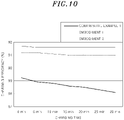
- FIG. 10 is a graph showing the variation of charging efficiency over time at different CR values when the receiving pad has a magnetic permeability of 300 or less.
- FIG. 11 is a graph showing the variation of heat generation temperature over time at different CR values when the receiving pad has a magnetic permeability of 300 or less.
- the receiving pad 210 when the receiving pad 210 includes a magnetic portion B having a magnetic permeability of 300 H/m or less, it can be found that the comparative example exhibits a degradation in charging efficiency over time, whereas the embodiment 1 and the embodiment 2 exhibit very little degradation over time.
- the magnetic portion B may be a ferrite, but the type of the magnetic portion B is not limited to ferrites.
- the receiving pad 210 includes the magnetic portion B having a magnetic permeability of 300 H/m or less, it can be seen that the embodiment 1 and the embodiment 2 exhibit a smaller increase in heat generation temperature compared to the comparative example 1, which leads to better efficiency in controlling heat generation temperature.
- the heat generation temperature according to the comparative example 1 rises at an increasingly fast pace over time during the first 10 minutes of the charging session but rises slowly over time after the first 10 minutes of the charging session. It can be seen that the heat generation temperatures according to the embodiment 1 and the embodiment 2 rise slowly throughout the entire charging session compared to the comparative example 1. Further, it can be seen that the heat generation temperature according to the embodiment 2 rises at an increasingly slow pace over time compared to the heat generation temperature according to the embodiment 1.
- the comparative example 1 exhibits a temperature variation rate of 5.51 °C/min
- the embodiment 1 exhibits a temperature variation rate of 2.94 °C/min
- the embodiment 2 exhibits a temperature variation rate of 1.66 °C/min, during 10 minutes from the charging start time (0 min). That is, the temperature variation rate according to the embodiment 1 may be less than or equal to 5.50 °C/min, less than or equal to 5.0 °C/min, less than or equal to 4.5 °C/min, less than or equal to 4.0 °C/min, less than or equal to 3.5 °C/min, and less than or equal to 3.0 °C/min between 0 and 10 minutes.
- the temperature variation rate according to the embodiment 2 may be less than or equal to 5.50 °C/min, less than or equal to 5.0 °C/min, less than or equal to 4.5 °C/min, less than or equal to 4.0 °C/min, less than or equal to 3.5 °C/min, less than or equal to 3.0 °C/min, less than or equal to 2.5 °C/min, less than or equal to 2.0 °C/min, less than or equal to 1.8 °C/min, and less than or equal to 1.7 °C/min between 0 and 10 minutes.
- the comparative example 1 exhibits a temperature variation rate of 3.84 °C/min
- the embodiment 1 exhibits a temperature variation rate of 2.54 °C/min
- the embodiment 2 exhibits a temperature variation rate of 1.41 °C/min, during 20 minutes from the charging start time (0 min). That is, the temperature variation rate according to the embodiment 1 may be less than or equal to 3.8 °C/min, less than or equal to 3.5 °C/min, less than or equal to 3.0 °C/min, less than or equal to 2.8 °C/min, and less than or equal to 2.6 °C/min between 0 and 20.
- the temperature variation rate according to the embodiment 2 may be less than or equal to 3.8 °C/min, less than or equal to 3.5 °C/min, less than or equal to 3.0 °C/min, less than or equal to 2.8 °C/min, less than or equal to 2.6 °C/min, less than or equal to 2.0 °C/min, less than or equal to 1.8 °C/min, and less than or equal to 1.5 °C/min between 0 and 20 minutes.
- the comparative example 1 exhibits a temperature variation rate of 3.09 °C/min
- the embodiment 1 exhibits a temperature variation rate of 2.14 °C/min
- the embodiment 2 exhibits a temperature variation rate of 1.09 °C/min, during 30 minutes from the charging start time (0 min). That is, the temperature variation rate according to the embodiment 1 may be less than or equal to 3.0 °C/min, less than or equal to 2.5 °C/min, less than or equal to 2.3 °C/min, and less than or equal to 2.2 °C/min between 0 and 30 minutes.
- the temperature variation rate according to the embodiment 2 may be less than or equal to 3.0 °C/min, less than or equal to 2.5 °C/min, less than or equal to 2.3 °C/min, less than or equal to 2.2 °C/min, less than or equal to 2.0 °C/min, less than or equal to 1.5 °C/min, and less than or equal to 1.3 °C/min between 0 and 30 minutes.
- the comparative example 1 exhibits a temperature variation rate of 2.16 °C/min
- the embodiment 1 exhibits a temperature variation rate of 2.13 °C/min
- the embodiment 2 exhibits a temperature variation rate of 1.15 °C/min, between 10 and 20 minutes from the charging start time (0 min). That is, the temperature variation rate according to the embodiment 1 may be less than or equal to 2.15 °C/min and less than or equal to 2.14 °C/min between 10 and 20 minutes after the start of the charging.
- the temperature variation rate according to the embodiment 2 may be less than or equal to 2.15 °C/min, less than or equal to 2.14 °C/min, less than or equal to 2.0 °C/min, less than or equal to 1.5 °C/min, and less than or equal to 1.3 °C/min between 10 and 20 minutes after the start of the charging.
- the temperature variation rate according to the embodiment 2 may be less than or equal to 1.58 °C/min, less than or equal to 1.5 °C/min, less than or equal to 1.4 °C/min, less than or equal to 1.0 °C/min, and less than or equal to 0.6 °C/min between 20 and 30 minutes after the start of the charging.
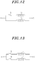
- the transmitting side resonant inductor L 1 of FIG. 2 is configured as, but not limited to, a single inductor, it may be formed in various structures.
- FIGS. 12 and 13 are views showing modifications of the transmitting side resonant inductor.
- the inductance of the transmitting side resonant inductor L 1 may be L 12 .
- the inductance of the transmitting side resonant inductor L 1 may be regulated, depending on whether the first switch S 1 is turned on/off.
- the wireless power transmitter 100 may regulate the inductance of the transmitting side resonant inductor L 1 by turning on/off the first switch S 1 depending on the inductance of the receiving side resonant inductor L 2 (i.e., the type of the wireless power receiver 200).
- the transmitting side resonant inductor L 1 may include a first inductor L 11 , a second inductor L 12 , a first switch S 1 , and a second switch S 2 .
- the inductance of the transmitting side resonant inductor L 1 may be L 11 .
- the inductance of the transmitting side resonant inductor L 1 may be L 12 .
- the wireless power transmitter 100 may include two transmitting side resonant inductors L 1 , so as to select the inductance of either of the two transmitting side resonant inductors L 1 depending on the CR to the receiving side resonant inductor and transmit power to the wireless power receiver 200.
- FIG. 14 is a view showing characteristics of charging efficiency and heat generation temperature according to an embodiment.
- the embodiment explained with reference to FIGS. 12 and 13 provides a configuration in which a plurality of transmitting side resonant inductors are included. Therefore, it is possible to measure charging efficiency and heat generation temperature even if the CR between the transmitting side resonant inductor and the receiving side resonant inductor varies, thereby improving the compatibility between the wireless power transmitter and the wireless power receiver.
Landscapes
- Engineering & Computer Science (AREA)
- Power Engineering (AREA)
- Computer Networks & Wireless Communication (AREA)
- Charge And Discharge Circuits For Batteries Or The Like (AREA)
- Burglar Alarm Systems (AREA)
- Input Circuits Of Receivers And Coupling Of Receivers And Audio Equipment (AREA)
- Remote Monitoring And Control Of Power-Distribution Networks (AREA)
Abstract
Description
- Embodiments of the present disclosure relates to a wireless power receiver and wireless power transmitter which receive and transmit wireless power.
- In general, wireless power transmission refers to a technology for supplying power to a means of transport using wireless electricity without a conventional wired power line. Various types of wireless power transmission are being developed due to advantages such as offering more user convenience in the use of electricity, reducing the risk of electrical shock, and enhancing aesthetical appearance.
- Notably, with growing interest in long-range wireless power transmission which can maximize user convenience, many related studies are actively underway.
- Conventional wireless power transceivers are configured by designing parameters for a resonant network, and their output power is determined by using the same configuration on a transmitting side resonant inductor and a receiving side resonant inductor.
- Magnetic materials are being used as the material of pads in recent years, in order to uniformly distribute a magnetic flux generated by transmitting/receiving pads used in wireless power transceivers. However, some of these magnetic materials are hard to apply in real-life settings where the inside of a space is enclosed, due to their low permeability and relatively high heat generation.
- To address the aforementioned problems, embodiments of the present disclosure provides a wireless power receiver and a wireless power transmitter for controlling current and magnetic flux in consideration of the characteristics of magnetic materials of pads used in the wireless power transceiver.
- Further, embodiments of the present disclosure provides a wireless power receiver and a wireless power transmitter for reducing heat generated by pads used in the wireless power transceiver.
- A wireless power receiver according to an embodiment includes: a receiving pad configured to receive power transmitted from a wireless power transmitter including a transmitting pad and a transmitting side resonant inductor; and a receiving side resonant network including a receiving side resonant inductor that controls power supplied to the receiving pad, and a first inductance of the receiving side resonant inductor and a second inductance of the transmitting side resonant inductor are determined to be different from each other.
- Further, the first inductance of the receiving side resonant inductor may be determined to be lower than the second inductance of the transmitting side resonant inductor.
- Further, the ratio of the first inductance to the second inductance may be determined to be less than 1.
- Further, when the receiving pad has a permeability greater than 300 and the ratio between the first inductance and the second inductance is less than 1, a heat generation temperature variation rate measured during 30 minutes from the time the power is received from the wireless power transmitter may be less than or equal to 2.0.
- Further, when the receiving pad has a permeability greater than 300 and the ratio between the first inductance and the second inductance is less than 1, a heat generation temperature variation rate measured during 10 minutes from the time the power is received from the wireless power transmitter may be less than or equal to 3.1.
- Further, when the receiving pad has a permeability of 300 or less and the ratio between the first inductance and the second inductance is less than 1, a heat generation temperature variation rate measured during 30 minutes from the time the power is received from the wireless power transmitter may be less than or equal to 3.00.
- A wireless power transmitter according to the embodiment includes: a transmitting pad configured to transmit power to a wireless power receiver including a receiving pad and a receiving side resonant inductor; and a transmitting side resonant network including a transmitting side resonant inductor that controls power supplied to the transmitting pad, and a first inductance of the receiving side resonant inductor and a second inductance of the transmitting side resonant inductor are determined to be different from each other.
- Further, the first inductance of the receiving side resonant inductor may be determined to be lower than the second inductance of the transmitting side resonant inductor, and the ratio of the first inductance to the second inductance may be determined to be less than 1.
- Further, when the transmitting pad has a permeability greater than 300 and the ratio between the first inductance and the second inductance is less than 1, a heat generation temperature variation rate measured during 30 minutes from the time the power is transmitted to the wireless power receiver may be less than or equal to 2.0. When the transmitting pad has a permeability greater than 300 and the ratio between the first inductance and the second inductance is less than 1, a heat generation temperature variation rate measured during 20 minutes from the time the power is transmitted to the wireless power receiver may be less than or equal to 2.4. Further, when the transmitting pad has a permeability greater than 300 and the ratio between the first inductance and the second inductance is less than 1, a heat generation temperature variation rate measured during 10 minutes from the time the power may be transmitted to the wireless power receiver is less than or equal to 3.1.
- Further, when the transmitting pad has a permeability of 300 or less and the ratio between the first inductance and the second inductance is less than 1, a heat generation temperature variation rate measured during 30 minutes from the time the power is transmitted to the wireless power receiver may be less than or equal to 3.00. when the transmitting pad has a permeability of 300 or less and the ratio between the first inductance and the second inductance is less than 1, a heat generation temperature variation rate measured during 20 minutes from the time the power is transmitted to the wireless power receiver may be less than or equal to 3.8. Further, when the transmitting pad has a permeability of 300 or less and the ratio between the first inductance and the second inductance is less than 1, a heat generation temperature variation rate measured during 10 minutes from the time the power is transmitted to the wireless power receiver may be less than or equal to 5.50.
- A means of transport according to the embodiment includes: a wireless power receiver including a receiving pad configured to receive power transmitted from a wireless power transmitter having a transmitting pad and a transmitting side resonant inductor, and a receiving side resonant network having a receiving side resonant inductor that controls power supplied to the receiving pad; and a battery that is charged with power received by using the wireless power receiver, and a first inductance of the receiving side resonant inductor and a second inductance of the transmitting side resonant inductor are determined to be different from each other.
- According to the embodiments, it is possible to reduce heat generated by transmission/reception pads by designing a transmitting side resonant inductor and a receiving side resonant inductor asymmetrically.
- Further, according to the embodiments, it is possible to uniformly distribute a magnetic flux through the transmission/reception pads by optimizing the inductances of the transmitting side resonant inductor and the receiving side resonant inductor.
- Further, according to the embodiments, it is possible to control heat generation more efficiently by taking the material of transmitting/receiving pads into consideration.
- Further, according to the embodiments, it is possible to improve the compatibility between the wireless power transmitter and the wireless power receiver even with different CR values, by varying the configuration of the transmitting side resonant inductor.
-
-
FIG. 1 is a block diagram showing a wireless power transceiver according to an embodiment. -
FIG. 2 is a circuit diagram of the wireless power transceiver ofFIG. 1 . -
FIG. 3 is a graph showing the change of the value of receiving coil current and the value of transmitting coil current versus CR. -
FIG. 4 is a graph showing the change of the value of transmitting coil magnetic flux and the value of receiving coil magnetic flux versus CR. -
FIG. 5 is a view showing the variation of magnetic flux distribution in the transmitting and receiving pads versus CR. -
FIG. 6 is a table showing the charging efficiency and heat generation temperature over time at different CR values when the receiving pad has a magnetic permeability greater than 300. -
FIG. 7 is a graph showing the charging efficiency over time at different CR values when the receiving pad has a magnetic permeability greater than 300. -
FIG. 8 is a graph showing the heat generation temperature over time at different CR values when the receiving pad has a magnetic permeability greater than 300. -
FIG. 9 is a table showing the charging efficiency and heat generation temperature over time at different CR values when the receiving pad has a magnetic permeability of 300 or less. -
FIG. 10 is a graph showing the charging efficiency over time at different CR values when the receiving pad has a magnetic permeability of 300 or less. -
FIG. 11 is a graph showing the heat generation temperature over time at different CR values when the receiving pad has a magnetic permeability of 300 or less. -
FIGS. 12 and 13 are views showing modifications of the transmitting side resonant inductor. -
FIG. 14 is a view showing characteristics of charging efficiency and heat generation temperature according to an embodiment. - Hereinafter, an exemplary embodiment of the present disclosure will be described in detail with reference to the accompanying drawings.
-
FIG. 1 is a block diagram showing a wireless power transceiver according to an embodiment of the present disclosure.FIG. 2 is a circuit diagram of the wireless power transceiver ofFIG. 1 . - Referring to
FIGS. 1 and2 , thewireless power transceiver 1000 according to the embodiment may include awireless power transmitter 100 and awireless power receiver 200. - The
wireless power transmitter 100 may include avoltage converter 110, a transmittingside resonant network 120, and a transmittingpad 130. - The
voltage converter 110 may convert a first input voltage UDC of DC into an AC voltage. - The
voltage converter 110 may include a plurality of rectifiers Q1, Q2, Q3, and Q4, and each of the rectifiers Q1, Q2, Q3, and Q4 may include an inverter (e.g., MOSFET) and a converter (e.g., diode). - The connections between the rectifiers Q1, Q2, Q3, and Q4 included in the
voltage converter 110 are as follows. A positive terminal of the first input voltage UDC, one end (e.g., drain of MOSFET) of the first rectifier Q1, and one end (e.g., drain of MOSFET) of the third rectifier Q3 may be connected to a fourth node D, and the other end (e.g., source of MOSFET) of the first rectifier Q1 and one end (e.g., drain of MOSFET) of the second rectifier Q2 may be connected to a first node A. - Further, one end (e.g., drain of MOSFET) of the fourth rectifier Q4 and the other end (e.g., source of MOSFET) of the third rectifier Q3 may be connected to a second node B, and the other end (e.g., source of MOSFET) of the second rectifier Q2 and the other end (e.g., source of MOSFET) of the fourth rectifier Q4 may be connected to a third node C.
- The transmitting
side resonant network 120 may be connected to thevoltage converter 110. The transmittingside resonant network 120 may receive a second input voltage UAB as input which is the voltage difference between the first node A and the second node B. The second input voltage UAB may be an AC voltage. - The transmitting
side resonant network 120 may include a transmitting side resonant inductor L1, a first transmitting side resonant capacitor Cf1, and a second transmitting side resonant capacitor Cp1. - The connections between impedances included in the transmitting side
resonant network 120 are as follows. One end of the transmitting side resonant inductor L1, one end of the first transmitting side resonant capacitor Cf1, and one end of the second transmitting side resonant capacitor Cp1 may be connected to a fifth node E, the other end of the second transmitting side resonant capacitor Cp1 may be connected to the second node B, and the other end of the transmitting side resonant inductor L1 may be connected to the first node A. - The transmitting
side resonant network 120 may be implemented on an input voltage line that connects a pair of legs constituting thevoltage converter 110. That is, the other end of the transmitting side resonant inductor L1 and the other end of the second transmitting side resonant capacitor Cp1 may be connected to thevoltage converter 110. - The
transmitting pad 130 may be made of a magnet or a magnetic composite. Here, the magnet may have a permeability greater than 300 H/m, and the magnetic composite may have a permeability of 300 H/m or less. - Moreover, the magnet may include a ferrite, and the magnetic composite may include a polymer magnetic composite including a binder resin and fillers distributed in the binder resin. The polymer magnetic composite may include a polymer magnetic block PMB. However, the types of magnet and magnetic composite are not limited to the above examples.
- The polymer magnetic composite may have less defects over a wide area and receive less damage from impacts as the fillers are held together by the binder resin.
- The fillers may be oxide fillers such as ferrites (Ni-Zn, Mg-Zn, and Mn-Zn ferrites); metallic fillers such as permalloy, sendust, and nanocrystalline magnetic material; or a powder mixture thereof. More specifically, the fillers may be sendust particles with an alloy composition of Fe-Si-Al.
- For example, the fillers may have a composition with the following Chemical Formula 1:
<Chemical Formula 1> Fe1-a-b-c Sia Xb Yc
where X may be Al, Cr, Ni, Cu, or a combination thereof; Y may be Mn, B, Co, Mo, or a combination thereof; and 0.01 ≤ a ≤ 0.2, 0.01 ≤ b ≤ 0.1, and 0 ≤ c ≤ 0.05. Specifically, in the above formula, X may be Al, Cr, or a combination thereof. - The fillers may include sendust.
- The average particle diameter D50 of the fillers may range from around 1 µm to 300 µm, from around 10 µm to 200 µm, or from around 30 µm to 150 µm. If the average particle diameter of the fillers meets the above range, the rate of change of position at temperatures from 150 °C to 180 °C may be made as low as possible, thereby further improving the heat resistance properties and magnetic properties of the magnetic composite and therefore leading to better charging efficiency.
- The fillers may make up 60 %, 70%, or 85 % by weight or more of the total weight of the polymer magnetic composite.
- For example, the filler content of the polymer magnetic composite may range from 60 % to 90 % by weight, from 70 % to 90 % by weight, from 75 % to 90 % by weight, from 78 % to 90 % by weight, from 80 % to 90 % by weight, from 85 % to 90 % by weight, from 87 % to 90 % by weight, or from 89 % to 90 % by weight. If the filler content is less than 60 % by weight, the rate of change of the position of the polymer magnetic composite increases and therefore the heat resistance properties of the magnetic composite degrade, which may cause deformation of and damage to the magnetic composite at high temperatures and weaken its magnetic properties and lower its charging efficiency.
- The melting point Tm of the binder resin may range from 150 °C to 210 °C. For example, the melting point Tm of the binder resin may range from 160 °C to 200 °C, e.g., from 160 °C to 180 °C. If the melting point Tm of the binder resin meets the above range, the rate of change of position at temperatures of 150 °C to 180 °C may be made as low as possible, thereby further improving the heat resistance properties and magnetic properties of the magnetic composite and therefore leading to better charging efficiency.
- The binder resin may include one or more selected from the group consisting of polyimide resin, polyamide resin, polyamide-imide resin, polycarbonate resin, acrylonitrile butadiene styrene (ABS) resin, polypropylene resin, polyethylene resin, polystyrene resin, polyphenylene sulfide (PPS) resin, polyether ether ketone (PEEK) resin, silicone resin, acrylic resin, polyurethane resin, polyester resin, isocyanate resin, and epoxy resin.
- The binder resin may be a curable resin. Specifically, the binder resin may be a photocurable resin and/or a thermosetting resin, especially a resin that can be cured and adhesive. More specifically, the binder resin may be a resin containing one or more thermally curable functional groups or sites such as a glycidyl group, an isocyanate group, a hydroxy group, a carboxyl group, or an amide group; or one or more functional groups or sites that are curable by an activated energy, such as an epoxide group, a cyclic ether group, a sulfide group, an acetal group, or a lactone group. Examples of these functional groups or sites may include an isocyanate group (-NCO), a hydroxy group (-OH), or a carboxyl group (-COOH).
- Specifically, the binder resin may include one or more selected from the group consisting of polyamide resin, polycarbonate resin, and polypropylene resin.
- Moreover, even the use of a resin with good heat resistance properties as the binder resin may increase the rate of change of position at temperatures of 150 °C to 180 °C unless it mixes well with the fillers. Accordingly, it may be important to choose the material of the binder resin that mixes well with the fillers.
- For example, a polyamide resin may be used as the binder resin, and sendust may be used as the fillers.
- The binder resin content of the polymer magnetic composite may range from 5 % to 40 % by weight, from 10 % to 40 % by weight, from 10 % to 20 % by weight, from 5 % to 20 % by weight, from 5 % to 15 % by weight, or from 7 % to 15 % by weight.
- According to one embodiment, the binder resin content may range from 10 % to 40 % by weight, and the filler content may range 60 % to 90 % by weight, in order that the rate of change of the position of the polymer magnetic composite is controlled to be 20 % or less at temperatures of 150 °C to 180 °C.
- According to one embodiment, the binder resin content may range from 10 % to 20 % by weight, and the filler content may range from 80 % to 90 % by weight, in order that the rate of change of the position of the polymer magnetic composite is controlled to be 3 % or less at temperatures of 150 °C to 180 °C.
- Furthermore, the polymer magnetic composite may further include an additive. Specifically, the polymer magnetic composite may further include one or more insulating coating agents selected from the group consisting of phosphoric acid and silane. The additive and the insulating coating agent may range from 0.1 % to 10 % by weight of the total weight of the polymer magnetic composite.
- If the additive content is within the above range, it is easier to reduce the rate of change of position at temperatures of 150 °C to 180 °C, thereby improving charging efficiency.
- The polymer magnetic composite may be elongated by a certain percentage. For example, the polymer magnetic composite may have an elongation of 0.5 % or more. Elongation properties are hard to obtain from ceramic magnetic composites which do not use polymer, and help reduce damage to large-area magnetic components even if they are distorted by impact. Specifically, the polymer magnetic composite may have an elongation of 0.5 % or more, 1 % or more, or 2.5 % or more. Although there is no upper limit for elongation, increasing the polymer resin content may degrade the physical properties of the magnetic composite, such as inductance, so it is desirable to keep the elongation at or below 10 %.
- The
transmitting pad 130 may include a flat-sheet structure, a stepwise structure, or a sandwiched structured. Thetransmitting pad 130 may include a transmitting coil LP. The transmitting coil LP may transmit electrical energy to a receiving coil LS without physical contact between electrodes via a magnetic field. - The
wireless power receiver 200 may include areceiving pad 210, a receiving sideresonant network 220, arectifying section 230, and aload section 240. - The
receiving pad 210 may be made of a magnet or a magnetic composite. Here, the magnet may have a permeability greater than 300 H/m, and the magnetic composite may have a permeability of 300 H/m or less. The magnet may include a ferrite, and the magnetic composite may include a polymer magnetic composite including a binder resin and fillers distributed in the binder resin. The polymer magnetic composite may include a polymer magnetic block PMB However, the types of magnet and magnetic composite are not limited to the above examples. A description of the polymer magnetic composite will be omitted since it will be redundant with the foregoing description of thetransmitting pad 130. - The
receiving pad 210 may include a receiving coil LS. - The receiving side
resonant network 220 may be configured in the same manner as the transmitting sideresonant network 120. That is, the receiving sideresonant network 220 may include a receiving side resonant inductor L2, a first receiving side resonant capacitor Cf2, and a second receiving side resonant capacitor Cp2. - Similar to the transmitting side
resonant network 120, one end of the first receiving side resonant capacitor Cf2 and one end of the receiving side resonant inductor L2 may be connected to a sixth node F. The other end of the receiving side resonant inductor L2 may be connected to a seventh node G. Further, one end of the second receiving side resonant capacitor Cp2 may be connected to the sixth node F, and the other end of the second receiving side resonant capacitor Cp2 may be connected to the seventh node H. - The rectifying
section 230 is a full bridge circuit with a plurality of diodes D1, D2, D3, and D4, which may rectify a voltage received from the receiving sideresonant network 220 by the diodes D1, D2, D3, and D4 and transmit it to theload section 240. - One end of the first diode D1 and one end of the third diode D3 may be connected to an eighth node H, and the other end of the first diode D1 and one end of the second diode D2 may be connected to the seventh node G. The other end of the third diode D3 and one end of the fourth diode D4 may be connected to the ninth node I, and the other end of the second diode D2 and the other end of the fourth diode D4 may be connected to a tenth node J.
- The
load section 240 is comprised of an output capacitor Co and a load resistor RL, in which case the load resistor RL may be a battery. Both ends of the output capacitor Co may be connected to upper and lower contact points of the full bridge circuit constituting therectifying section 230 and receive a rectified output voltage through the rectifyingsection 230. For example, both ends of the output capacitor Co may be connected between the eight node H and the tenth node J. - Meanwhile, the transmitting side
resonant network 120 and the receiving sideresonant network 220 may compensate for an impedance between the transmitting coil LP of thetransmitting pad 130 and the receiving coil LS of thereceiving pad 210. - To this end, the inductance of the transmitting side resonant inductor L1 of the transmitting side
resonant network 120 and the inductance of the receiving side resonant inductor L2 of the receiving sideresonant network 220 may be set. The inductance of the transmitting side resonant inductor L1 and the inductance of the receiving side resonant inductor L2 may be set based on size and weight limitations of the transmitting and receiving coils. - As in
equation 1, an output current Io of the receiving sideresonant network 220 may be inversely proportional to the product of the inductance of the transmitting side resonant inductor L1 and the inductance of the receiving side resonant inductor L2.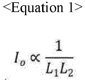
- As in
equation 2, a transmitting coil current Ip of the transmitting sideresonant network 120 may be inversely proportional the inductance of the transmitting side resonant inductor L1.
- As shown in
FIG. 3 , a receiving coil current Is of thereceiving pad 210 may be inversely proportional to the product of the inductance of the transmitting side resonant inductor L1 and the square of the inductance of the receiving side resonant inductor L2.
- In an embodiment, when determining the output power, the inductance of the transmitting side resonant inductor L1 and the inductance of the receiving side resonant inductor L2 may be regulated or changed to vary the transmitting coil current Ip that is the current at the transmitting side and the receiving coil current Is that is the current at the receiving side.
- For example, when the product of the transmitting side resonant inductor L1 and the receiving side resonant inductor L2 is constant, increasing the transmitting side resonant inductor L1 and decreasing the receiving side resonant inductor L2 may decrease the transmitting coil current Ip and increase the receiving coil current Is. Inversely, decreasing the transmitting side resonant inductor L1 and increasing the receiving side resonant inductor L2 may increase the transmitting coil current Ip and decrease the receiving coil current Is.
- The inductance of the transmitting side resonant inductor L1 may be defined as in equation 4. Here, the CR (current ratio) is a coefficient determined based on the transmitting side resonant inductor L1 and the receiving side resonant inductor L2.

- The inductance of the receiving side resonant inductor L2 may be defined as in equation 5:

where L' may be calculated by using the first input voltage UDC, an output power Po, a load resistance Ro, the coupling coefficient k of thewireless power transmitter 100 and thewireless power receiver 200, the resonant frequency Wo of thewireless power transmitter 100 and thewireless power receiver 200, and the inductances of the transmitting coil Lp and receiving coil Ls, as in equation 6. - According to equation 4 and
equation 5, the CR may be

- In an embodiment, when the CR is determined by equation 4 and
equation 5, the transmitting coil current Ip and the receiving coil current Is may be determined to be inversely proportional to each other. - Accordingly, once the transmitting coil current Ip and the receiving coil current Is are regulated, current loss occurring in the
transmitting pad 130 and thereceiving pad 210 may be regulated and therefore the amount of heat generation in each of thewireless power transmitter 100 and thewireless power receiver 200 may be regulated. - For example, if a material with low magnetic properties is used for the receiving pad 1210, the heat generation of the
receiving pad 210 may be reduced by decreasing the receiving coil current Is and increasing the transmitting coil current Ip, thereby improving overall efficiency. - Moreover, the magnetic flux ϕp of the
transmitting pad 130 may be determined by equation 7, and the magnetic flux ϕs of thereceiving pad 210 may be determined by equation 8.

where Lpk1 is the leakage inductance of the transmitting coil Lp, Lsk2 is the leakage inductance of the receiving coil Ls, Lm is magnetizing inductance, and ILM is magnetizing current. - As in equation 7 and equation 8, it can be seen that the magnetic flux ϕp of the
transmitting pad 130 and the magnetic flux ϕs of thereceiving pad 210 are affected by the transmitting coil current Ip and the receiving coil current Is. - Accordingly, controlling the CR makes it possible to regulate magnetic flux distribution such that there is no magnetic flux locally generated in the transmitting and receiving
pads pads -
FIG. 3 is a graph showing the change of the value of the receiving coil current Is and the value of transmitting coil current Ip versus CR.FIG. 4 is a graph showing the change of the value of the transmitting coil magnetic flux and the value of receiving coil magnetic flux versus CR. - Referring to
FIG. 2 andFIG. 3 in which the magnitude of the transmitting coil current Ip and the magnitude of the receiving coil current Is are compared with respect to CR, it can be seen that the transmitting coil current Ip is greater than the receiving coil current Is when the CR is less than or equal to approximately 1.1. On the other hand, it can be seen that the transmitting coil current Ip is smaller than the receiving coil current Is when the CR is greater than approximately 1.1. Here, it is presumed that the transmitting and receivingpads - Further, referring to
FIG. 2 andFIG. 4 in which the magnetic fluxes of the transmitting and receivingpads FIG. 3 with respect to CR, it can be seen that the magnetic flux ϕp of the transmitting coil is greater than the magnetic flux ϕs of the receiving coil when the CR is less than or equal to approximately 0.9, and that the magnetic flux ϕp of the transmitting coil is smaller than the magnetic flux ϕs of the receiving coil when the CR is greater than approximately 0.9. - By setting the CR to be less than or equal to approximately 0.9, the current and magnetic flux of the receiving coil become smaller than the current and magnetic flux of the transmitting coil, which may reduce the heat generation in the
receiving pad 210. - If the CR is less than approximately 0.6, it is difficult to achieve inductance, making it difficult to measure the currents and magnetic fluxes of the transmitting and receiving coils. Therefore, the CR may be set to a value of 0.6 to 0.9.
-
FIG. 5 is a view showing the variation of magnetic flux distribution in the transmitting and receiving pads versus CR. - Referring to
FIGS. 2 and5 , it can be seen that, when the CR is 1.0, thetransmitting pad 130 may have a magnetic flux density of 43.5 and the receiving pad may have a magnetic flux density of 77. 5. On the other hand, it can be seen that, when the CR is 0.8, the transmitting pad may have a magnetic flux density of 51.2 and the receiving pad may have a magnetic flux density of 63. - When the CR is 0.8, it can be seen that the
receiving pad 210 has a lower magnetic flux density and a more uniform magnetic flux distribution over the entire area of thereceiving pad 210, as compared to when the CR is 1, which results in less heat generation. - Hereinafter, a process of measuring charging efficiency and heat generation temperature with respect to the material of the transmitting pad and receiving pad and the CR will be described.
- For measurement, the charging frequency was set to 85 kHz, and voltage and current were supplied using a power supply. Moreover, E-Load, which is used for performance diagnostic testing, was connected to a tip end of the
wireless power receiver 200. In addition, the output power was set to 8.8 kW, and the charging efficiency and heat generation temperature of thereceiving pad 210 were measured for an operation time of 30 minutes. - When there is a need to control the heat generation temperature of the
receiving pad 130, the CR may be designed as CR < 1, and when there is a need to control the heat generation temperature of thetransmitting pad 230 because thereceiver 200 is easily cooled, the CR may be designed as CR ≥ 1. - In a case where the
wireless power transceiver 1000 according to an embodiment of the present disclosure is applied to a means of transport powered by electricity (e.g., electric vehicle, electric bicycle, drone, electric kickboard, an electric motorcycle, etc.), thewireless power transmitter 100 may be installed at a charging station, and thewireless power receiver 200 may be installed at the means of transport. In this case, the means of transport may be limited in heat dissipation compared to the charging station due to size limitations, technical limitations, and so on, which calls for a method for reducing the heat generation in the means of transport. - Accordingly, in order to reduce the heat generation in the means of transport, the inductance of the transmitting side resonant inductor L1 included in the
wireless power transmitter 100 and/or the inductance of the receiving side resonant inductor L2 included in thewireless power receiver 200 may be regulated, and therefore the heat generation temperature of thereceiving pad 130 may be reduced, which may lead to, but not limited to, a reduction in the heat generation in the means of transport. That is, the above description may apply equally to reducing the heat generation in the charging station, as well as to reducing the heat generation in the means of transport. - The ratio (CR) of the inductance of the transmitting side resonant inductor L1 to the inductance of the receiving side resonant inductor L2 may be less than 1. Further, the ratio (CR) of the inductance of the transmitting side resonant inductor L1 to the inductance of the receiving side resonant inductor L2 may be greater than or equal to 0.6, 0.7, or 0.8.
- Hereinafter, a comparative example 1 in which the CR is 1, an
embodiment 1 in which the CR is 0.8, and anembodiment 2 in which the CR is 0.6 will be described by way of example. - The following description concerning variation rates of the charging efficiency and heat generation temperature with respect to CR will be given of, but not limited to, the receiving pad. That is, the description below may equally apply to the transmitting pad.
-
FIG. 6 is a table showing the charging efficiency and heat generation temperature over time at different CR values when the receiving pad has a magnetic permeability greater than 300.FIG. 7 is a graph showing the variation of the charging efficiency over time at different CR values when the receiving pad has a magnetic permeability greater than 300.FIG. 8 is a graph showing the variation of the heat generation temperature over time at different CR values when the receiving pad has a magnetic permeability greater than 300. - Referring to
FIG. 2 ,FIG. 6 ,FIG. 7 , andFIG. 8 , when thereceiving pad 210 includes a predetermined magnetic portion A in which a magnetic permeability is greater than 300 H/m, it can be found that theembodiment 1 exhibits higher charging efficiency and lower heat generation temperature in the entire area compared to the comparative example 1. For example, the magnetic portion A may be a ferrite, but the type of the magnetic portion A is not limited to ferrites. - For example, referring to
FIG. 6 , it can be found that the temperature variation rate in the comparative example 1 is 3.16 °C/min and the temperature variation rate in theembodiment 1 is 2.81 °C/min, during 10 minutes from the charging start time (0 min). That is, it can be seen that the temperature variation rate in theembodiment 1 is less than or equal to 3.1 °C/min, less than or equal to 3.0 °C/min, less than or equal to 2.9 °C/min, and less than or equal to 2.85 °C/min during 10 minutes from the charging start time (0 min). - Further, it can be found that the temperature variation rate in the comparative example is 2.48 °C/min and the temperature variation rate in the
embodiment 1 is 2.09 °C/min, during 20 minutes from the charging start time (0 min). That is, it can be seen that the temperature variation rate in theembodiment 1 is less than or equal to 2.4 °C/min, less than or equal to 2.3 °C/min, less than or equal to 2.2 °C/min, and less than or equal to 2.1 °C/min during 20 minutes from the charging start time (0 min). - Further, it can be found that the temperature variation rate in the comparative example is 2.01 °C/min and the temperature variation rate in the
embodiment 1 is approximately 1.58 °C/min, during 30 minutes from the charging start time (0 min). That is, it can be seen that the temperature variation rate in theembodiment 1 is less than or equal to 2.0 °C/min, less than or equal to 1.9 °C/min, less than or equal to 1.8 °C/min, less than or equal to 1.7 °C/min, and less than or equal to 1.6 °C/min, during 30 minutes from the charging start time (0 min). - Further, it can be found that the temperature variation rate in the comparative example is 1.8 °C/min and the temperature variation rate in the
embodiment 1 is 1.37 °C/min, between 10 minutes and 20 minutes after the start of the charging. That is, it can be seen that the temperature variation rate in theembodiment 1 is less than or equal to 1.7 °C/min, less than or equal to 1.6 °C/min, less than or equal to 1.5 °C/min, and less than or equal to 1.4 °C/min, between 10 minutes and 20 minutes after the start of the charging. - Further, it can be found that the temperature variation rate in the comparative example is 1.07 °C/min and the temperature variation rate in the
embodiment 1 is 0.57 °C/min, between 20 minutes and 30 minutes after the start of the charging. That is, it can be seen that the temperature variation rate in theembodiment 1 is less than or equal to 1.0 °C/min, less than or equal to 0.9 °C/min, less than or equal to 0.8 °C/min, less than or equal to 0.7 °C/min, and less than or equal to 0.6 °C/min between 20 minutes and 30 minutes after the start of the charging. - Further, the charging efficiency in the
embodiment 1 may be greater than or equal to 91.1 and greater than or equal to 91.3 during 30 minutes after the start of the charging. -
FIG. 9 is a table showing the charging efficiency and heat generation temperature over time at different CR values when the receiving pad has a magnetic permeability of 300 or less.FIG. 10 is a graph showing the variation of charging efficiency over time at different CR values when the receiving pad has a magnetic permeability of 300 or less.FIG. 11 is a graph showing the variation of heat generation temperature over time at different CR values when the receiving pad has a magnetic permeability of 300 or less. - Referring to
FIG. 2 ,FIG. 9 ,FIG. 10 , andFIG. 11 , when thereceiving pad 210 includes a magnetic portion B having a magnetic permeability of 300 H/m or less, it can be found that the comparative example exhibits a degradation in charging efficiency over time, whereas theembodiment 1 and theembodiment 2 exhibit very little degradation over time. For example, the magnetic portion B may be a ferrite, but the type of the magnetic portion B is not limited to ferrites. - Moreover, when the
receiving pad 210 includes the magnetic portion B having a magnetic permeability of 300 H/m or less, it can be seen that theembodiment 1 and theembodiment 2 exhibit a smaller increase in heat generation temperature compared to the comparative example 1, which leads to better efficiency in controlling heat generation temperature. - Additionally, it can be seen that the heat generation temperature according to the comparative example 1 rises at an increasingly fast pace over time during the first 10 minutes of the charging session but rises slowly over time after the first 10 minutes of the charging session. It can be seen that the heat generation temperatures according to the
embodiment 1 and theembodiment 2 rise slowly throughout the entire charging session compared to the comparative example 1. Further, it can be seen that the heat generation temperature according to theembodiment 2 rises at an increasingly slow pace over time compared to the heat generation temperature according to theembodiment 1. - Referring to
FIG. 9 , it can be found that the comparative example 1 exhibits a temperature variation rate of 5.51 °C/min, theembodiment 1 exhibits a temperature variation rate of 2.94 °C/min, and theembodiment 2 exhibits a temperature variation rate of 1.66 °C/min, during 10 minutes from the charging start time (0 min). That is, the temperature variation rate according to theembodiment 1 may be less than or equal to 5.50 °C/min, less than or equal to 5.0 °C/min, less than or equal to 4.5 °C/min, less than or equal to 4.0 °C/min, less than or equal to 3.5 °C/min, and less than or equal to 3.0 °C/min between 0 and 10 minutes. The temperature variation rate according to theembodiment 2 may be less than or equal to 5.50 °C/min, less than or equal to 5.0 °C/min, less than or equal to 4.5 °C/min, less than or equal to 4.0 °C/min, less than or equal to 3.5 °C/min, less than or equal to 3.0 °C/min, less than or equal to 2.5 °C/min, less than or equal to 2.0 °C/min, less than or equal to 1.8 °C/min, and less than or equal to 1.7 °C/min between 0 and 10 minutes. - Further, it can be found that the comparative example 1 exhibits a temperature variation rate of 3.84 °C/min, the
embodiment 1 exhibits a temperature variation rate of 2.54 °C/min, and theembodiment 2 exhibits a temperature variation rate of 1.41 °C/min, during 20 minutes from the charging start time (0 min). That is, the temperature variation rate according to theembodiment 1 may be less than or equal to 3.8 °C/min, less than or equal to 3.5 °C/min, less than or equal to 3.0 °C/min, less than or equal to 2.8 °C/min, and less than or equal to 2.6 °C/min between 0 and 20. Further, the temperature variation rate according to theembodiment 2 may be less than or equal to 3.8 °C/min, less than or equal to 3.5 °C/min, less than or equal to 3.0 °C/min, less than or equal to 2.8 °C/min, less than or equal to 2.6 °C/min, less than or equal to 2.0 °C/min, less than or equal to 1.8 °C/min, and less than or equal to 1.5 °C/min between 0 and 20 minutes. - Further, it can be found that the comparative example 1 exhibits a temperature variation rate of 3.09 °C/min, the
embodiment 1 exhibits a temperature variation rate of 2.14 °C/min, and theembodiment 2 exhibits a temperature variation rate of 1.09 °C/min, during 30 minutes from the charging start time (0 min). That is, the temperature variation rate according to theembodiment 1 may be less than or equal to 3.0 °C/min, less than or equal to 2.5 °C/min, less than or equal to 2.3 °C/min, and less than or equal to 2.2 °C/min between 0 and 30 minutes. Further, the temperature variation rate according to theembodiment 2 may be less than or equal to 3.0 °C/min, less than or equal to 2.5 °C/min, less than or equal to 2.3 °C/min, less than or equal to 2.2 °C/min, less than or equal to 2.0 °C/min, less than or equal to 1.5 °C/min, and less than or equal to 1.3 °C/min between 0 and 30 minutes. - Further, it can be found that the comparative example 1 exhibits a temperature variation rate of 2.16 °C/min, the
embodiment 1 exhibits a temperature variation rate of 2.13 °C/min, and theembodiment 2 exhibits a temperature variation rate of 1.15 °C/min, between 10 and 20 minutes from the charging start time (0 min). That is, the temperature variation rate according to theembodiment 1 may be less than or equal to 2.15 °C/min and less than or equal to 2.14 °C/min between 10 and 20 minutes after the start of the charging. Further, the temperature variation rate according to theembodiment 2 may be less than or equal to 2.15 °C/min, less than or equal to 2.14 °C/min, less than or equal to 2.0 °C/min, less than or equal to 1.5 °C/min, and less than or equal to 1.3 °C/min between 10 and 20 minutes after the start of the charging. - Further, it can be found that the comparative example 1 exhibits a temperature variation rate of 1.59 °C/min, the
embodiment 1 exhibits a temperature variation rate of 1.36 °C/min, and theembodiment 2 exhibits a temperature variation rate of 0.47 °C/min, between 20 and 30 minutes from the charging start time (0 min). That is, the temperature variation rate according to theembodiment 1 may be less than or equal to 1.58 °C/min, less than or equal to 1.5 °C/min, and less than or equal to 1.4 °C/min between 20 and 30 minutes after the start of the charging. Further, the temperature variation rate according to theembodiment 2 may be less than or equal to 1.58 °C/min, less than or equal to 1.5 °C/min, less than or equal to 1.4 °C/min, less than or equal to 1.0 °C/min, and less than or equal to 0.6 °C/min between 20 and 30 minutes after the start of the charging. - Moreover, it can be seen that, when charging is performed for 30 minutes from the charging start time (0 min), the charging efficiency according to the
embodiment 1 and theembodiment 2 is greater than or equal to 88.2, greater than or equal to 88.5, greater than or equal to 89.0, greater than or equal to 89.3, greater than or equal to 90, and greater than or equal to 91. - As can be seen from
FIGS. 9 to 11 , better charging efficiency and lower heat generation temperature can be achieved when the CR is 0.6, compared to when the CR is 0.8 - that is, the lower the CR, the better the charging efficiency and the lower the heat generation temperature. - Meanwhile, although the transmitting side resonant inductor L1 of
FIG. 2 is configured as, but not limited to, a single inductor, it may be formed in various structures. -
FIGS. 12 and 13 are views showing modifications of the transmitting side resonant inductor. - Referring to
FIG. 12 , according to an embodiment, the transmitting side resonant inductor L1 may include a first inductor L11, a second inductor L12, and a first switch S1. In some embodiments, the first inductor L11 and the first switch S1 may be connected in series, and the first inductor L11 and the first switch S1 may be connected in parallel to the second inductor L12. - When the first switch S1 is turned on (ON), the inductance of the transmitting side resonant inductor may be calculated as in equation 9.

- On the other hand, when the first switch S1 is turned off (OFF), the inductance of the transmitting side resonant inductor L1 may be L12.
- That is, the inductance of the transmitting side resonant inductor L1 may be regulated, depending on whether the first switch S1 is turned on/off. As such, the
wireless power transmitter 100 may regulate the inductance of the transmitting side resonant inductor L1 by turning on/off the first switch S1 depending on the inductance of the receiving side resonant inductor L2 (i.e., the type of the wireless power receiver 200). - Moreover, referring to
FIG. 13 , according to another embodiment, the transmitting side resonant inductor L1 may include a first inductor L11, a second inductor L12, a first switch S1, and a second switch S2. - In some embodiments, the first inductor L11 and the first switch S1 may be connected in series, and the second inductor L12 and the second switch S2 may be connected in series. Further, the first inductor L11 and the first switch S1 may be connected in parallel to the second inductor L12 and the second switch S2.
- When the first switch S1 is turned on and the second switch S2 is turned off, the inductance of the transmitting side resonant inductor L1 may be L11. On the other hand, when the first switch S1 is turned off and the second switch S2 is turned on, the inductance of the transmitting side resonant inductor L1 may be L12.
- As illustrated in
FIG. 12 and FIG. 13 , thewireless power transmitter 100 may include two transmitting side resonant inductors L1, so as to select the inductance of either of the two transmitting side resonant inductors L1 depending on the CR to the receiving side resonant inductor and transmit power to thewireless power receiver 200. -
FIG. 14 is a view showing characteristics of charging efficiency and heat generation temperature according to an embodiment. - Conventionally, it was not possible to measure charging efficiency and heat generation temperature if the CR between the transmitting side resonant inductor and the receiving side resonant inductor varies.
- On the other hand, as illustrated in
FIG. 14 , the embodiment explained with reference toFIGS. 12 and 13 provides a configuration in which a plurality of transmitting side resonant inductors are included. Therefore, it is possible to measure charging efficiency and heat generation temperature even if the CR between the transmitting side resonant inductor and the receiving side resonant inductor varies, thereby improving the compatibility between the wireless power transmitter and the wireless power receiver. - While the above description has been made with reference to the embodiments and drawings, it will be understood by those skilled in the art to which this present disclosure belongs that various changes and modifications may be made without departing from the scope of embodiments as defined by the appended claims.
Claims (11)
- A wireless power receiver comprising:a receiving pad configured to receive power transmitted from a wireless power transmitter including a transmitting pad and a transmitting side resonant inductor; anda receiving side resonant network including a receiving side resonant inductor that controls power supplied to the receiving pad,wherein a first inductance of the receiving side resonant inductor and a second inductance of the transmitting side resonant inductor are determined to be different from each other.
- The wireless power receiver of claim 1, wherein the first inductance of the receiving side resonant inductor is determined to be lower than the second inductance of the transmitting side resonant inductor.
- The wireless power receiver of claim 2, wherein the ratio of the first inductance to the second inductance is determined to be less than 1.
- The wireless power receiver of claim 1, wherein, when the receiving pad has a permeability greater than 300 and the ratio between the first inductance and the second inductance is less than 1, a heat generation temperature variation rate measured during 30 minutes from the time the power is received from the wireless power transmitter is less than or equal to 2.0.
- The wireless power receiver of claim 1, wherein, when the receiving pad has a permeability greater than 300 and the ratio between the first inductance and the second inductance is less than 1, a heat generation temperature variation rate measured during 10 minutes from the time the power is received from the wireless power transmitter is less than or equal to 3.1.
- The wireless power receiver of claim 1, wherein, when the receiving pad has a permeability of 300 or less and the ratio between the first inductance and the second inductance is less than 1, a heat generation temperature variation rate measured during 30 minutes from the time the power is received from the wireless power transmitter is less than or equal to 3.00.
- A wireless power transmitter comprising:a transmitting pad configured to transmit power to a wireless power receiver including a receiving pad and a receiving side resonant inductor; anda transmitting side resonant network including a transmitting side resonant inductor that controls power supplied to the transmitting pad,wherein a first inductance of the receiving side resonant inductor and a second inductance of the transmitting side resonant inductor are determined to be different from each other.
- The wireless power transmitter of claim 7, wherein the first inductance of the receiving side resonant inductor is determined to be lower than the second inductance of the transmitting side resonant inductor, and the ratio of the first inductance to the second inductance is determined to be less than 1.
- The wireless power transmitter of claim 7, wherein, when the transmitting pad has a permeability greater than 300 and the ratio between the first inductance and the second inductance is less than 1, a heat generation temperature variation rate measured during 30 minutes from the time the power is transmitted to the wireless power receiver is less than or equal to 2.0,when the transmitting pad has a permeability greater than 300 and the ratio between the first inductance and the second inductance is less than 1, a heat generation temperature variation rate measured during 20 minutes from the time the power is transmitted to the wireless power receiver is less than or equal to 2.4, andwhen the transmitting pad has a permeability greater than 300 and the ratio between the first inductance and the second inductance is less than 1, a heat generation temperature variation rate measured during 10 minutes from the time the power is transmitted to the wireless power receiver is less than or equal to 3.1.
- The wireless power transmitter of claim 7, wherein, when the transmitting pad has a permeability of 300 or less and the ratio between the first inductance and the second inductance is less than 1, a heat generation temperature variation rate measured during 30 minutes from the time the power is transmitted to the wireless power receiver is less than or equal to 3.00,when the transmitting pad has a permeability of 300 or less and the ratio between the first inductance and the second inductance is less than 1, a heat generation temperature variation rate measured during 20 minutes from the time the power is transmitted to the wireless power receiver is less than or equal to 3.8, andwhen the transmitting pad has a permeability of 300 or less and the ratio between the first inductance and the second inductance is less than 1, a heat generation temperature variation rate measured during 10 minutes from the time the power is transmitted to the wireless power receiver is less than or equal to 5.50.
- A means of transport comprising:a wireless power receiver including a receiving pad configured to receive power transmitted from a wireless power transmitter having a transmitting pad and a transmitting side resonant inductor, and a receiving side resonant network having a receiving side resonant inductor that controls power supplied to the receiving pad; anda battery that is charged with power received by using the wireless power receiver,wherein a first inductance of the receiving side resonant inductor and a second inductance of the transmitting side resonant inductor are determined to be different from each other.
Applications Claiming Priority (2)
| Application Number | Priority Date | Filing Date | Title |
|---|---|---|---|
| KR1020200108384A KR102439634B1 (en) | 2020-08-27 | 2020-08-27 | Wireless power receiver apparatus, wireless power transfer apparatus and wireless power transceiving apparatus |
| PCT/KR2021/011511 WO2022045826A1 (en) | 2020-08-27 | 2021-08-27 | Wireless power reception device and wireless power transmission device |
Publications (2)
| Publication Number | Publication Date |
|---|---|
| EP4120510A1 true EP4120510A1 (en) | 2023-01-18 |
| EP4120510A4 EP4120510A4 (en) | 2024-04-03 |
Family
ID=80355516
Family Applications (1)
| Application Number | Title | Priority Date | Filing Date |
|---|---|---|---|
| EP21862122.5A Pending EP4120510A4 (en) | 2020-08-27 | 2021-08-27 | Wireless power reception device and wireless power transmission device |
Country Status (7)
| Country | Link |
|---|---|
| US (1) | US12381420B2 (en) |
| EP (1) | EP4120510A4 (en) |
| JP (1) | JP7457836B2 (en) |
| KR (1) | KR102439634B1 (en) |
| CN (1) | CN115552765A (en) |
| TW (1) | TWI779804B (en) |
| WO (1) | WO2022045826A1 (en) |
Family Cites Families (27)
| Publication number | Priority date | Publication date | Assignee | Title |
|---|---|---|---|---|
| KR101423406B1 (en) * | 2009-11-18 | 2014-07-24 | 가부시끼가이샤 도시바 | Wireless power transmission device |
| TWI389416B (en) * | 2010-05-31 | 2013-03-11 | 富達通科技股份有限公司 | Power transmission method of high power wireless inductive power supply |
| KR101312532B1 (en) * | 2010-10-29 | 2013-09-30 | 한국전기연구원 | Capacitive and Transformer Coupling Method for Resonance based Wireless Power Transfer |
| EP2648135B1 (en) * | 2010-11-29 | 2019-07-17 | Fujitsu Limited | Portable device and power supply system |
| KR101875942B1 (en) * | 2011-10-18 | 2018-07-06 | 엘지이노텍 주식회사 | Apparatus for receving wireless power and system for transmitting wireless power |
| EP2909917B1 (en) * | 2012-10-16 | 2020-11-11 | Koninklijke Philips N.V. | Wireless inductive power transfer |
| US9768643B2 (en) * | 2012-11-02 | 2017-09-19 | Panasonic Intellectual Property Management Co., Ltd. | Wireless power transmission system capable of continuing power transmission while suppressing heatup of foreign objects |
| KR102028059B1 (en) | 2012-12-27 | 2019-10-04 | 삼성전자주식회사 | Method and apparatus for resonating in wireless power transfer system |
| JP6216966B2 (en) | 2013-03-29 | 2017-10-25 | 株式会社エクォス・リサーチ | Power transmission system |
| KR20150000704A (en) * | 2013-06-25 | 2015-01-05 | 삼성전기주식회사 | Wireless transmitter-receiver using variable indutance pad |
| US10003217B2 (en) * | 2014-03-04 | 2018-06-19 | Qualcomm Incorporated | System and method for reducing emissions for polarized coil systems for wireless inductive power transfer |
| JP6464520B2 (en) | 2014-04-23 | 2019-02-06 | パナソニックIpマネジメント株式会社 | Non-contact power transmission device, non-contact power reception device, and non-contact power transmission system |
| TR201907901T4 (en) * | 2015-11-02 | 2019-06-21 | Koninklijke Philips Nv | Wireless inductive power transmission. |
| KR101773403B1 (en) * | 2015-11-20 | 2017-08-31 | 숭실대학교산학협력단 | Double sided resonant converter for wireless charger and method for implementing thereof |
| US10193534B2 (en) * | 2015-12-17 | 2019-01-29 | Garrity Power Services Llc | Wireless power system tuning apparatus |
| KR102523627B1 (en) * | 2015-12-23 | 2023-04-19 | 주식회사 아모센스 | wireless power transmission module having variable inductor |
| KR101843267B1 (en) * | 2016-07-07 | 2018-03-28 | 삼성전기주식회사 | Magnetic Sheet and Electronic Device |
| KR20180057069A (en) * | 2016-11-21 | 2018-05-30 | 엘지이노텍 주식회사 | Wireless Charging Method and Apparatus and System therefor |
| US20190074719A1 (en) * | 2017-09-06 | 2019-03-07 | Apple Inc. | Multiple-structure wireless charging receiver systems having multiple receiver coils |
| US10381881B2 (en) * | 2017-09-06 | 2019-08-13 | Apple Inc. | Architecture of portable electronic devices with wireless charging receiver systems |
| KR20190030019A (en) * | 2017-09-13 | 2019-03-21 | 엘지이노텍 주식회사 | Method for Transmitting Power for Each of Wireless Power Receiver and Wireless Power Transmitter |
| CN209462088U (en) * | 2018-07-16 | 2019-10-01 | 香港大学 | Wireless power transmission system |
| CN208674942U (en) * | 2018-08-23 | 2019-03-29 | 欧亚光能源科技股份有限公司 | Electric transportation tool wireless induction quick charging system and electric transportation tool |
| TWI699066B (en) * | 2018-11-07 | 2020-07-11 | 台灣立訊精密有限公司 | Wireless charging converting device and protection case having the same |
| JP2020115703A (en) | 2019-01-17 | 2020-07-30 | 株式会社Soken | Non-contact power transmission system |
| CN111146872B (en) * | 2019-12-31 | 2022-04-05 | 华为数字能源技术有限公司 | wireless power transfer system |
| CN111342565A (en) * | 2020-03-19 | 2020-06-26 | 许继集团有限公司 | Electric power wireless transmission coupling device and system |
-
2020
- 2020-08-27 KR KR1020200108384A patent/KR102439634B1/en active Active
-
2021
- 2021-08-27 CN CN202180034107.6A patent/CN115552765A/en active Pending
- 2021-08-27 WO PCT/KR2021/011511 patent/WO2022045826A1/en not_active Ceased
- 2021-08-27 TW TW110131893A patent/TWI779804B/en active
- 2021-08-27 JP JP2022564103A patent/JP7457836B2/en active Active
- 2021-08-27 EP EP21862122.5A patent/EP4120510A4/en active Pending
-
2022
- 2022-10-07 US US17/962,000 patent/US12381420B2/en active Active
Also Published As
| Publication number | Publication date |
|---|---|
| TWI779804B (en) | 2022-10-01 |
| JP2023522388A (en) | 2023-05-30 |
| CN115552765A (en) | 2022-12-30 |
| KR20220027480A (en) | 2022-03-08 |
| TW202215751A (en) | 2022-04-16 |
| WO2022045826A1 (en) | 2022-03-03 |
| US12381420B2 (en) | 2025-08-05 |
| KR102439634B1 (en) | 2022-09-05 |
| JP7457836B2 (en) | 2024-03-28 |
| EP4120510A4 (en) | 2024-04-03 |
| US20230057615A1 (en) | 2023-02-23 |
Similar Documents
| Publication | Publication Date | Title |
|---|---|---|
| US10002704B2 (en) | Coil module | |
| US11337345B2 (en) | Magnetic field shielding sheet for a wireless charger, method for manufacturing same, and receiving apparatus for a wireless charger using the sheet | |
| EP2482291B1 (en) | Magnetic powder material and low-loss composite magnetic material containing same | |
| CN105210234A (en) | Coil module, antenna device and electronic equipment | |
| JP2013060332A (en) | Ferrite plate | |
| KR102144824B1 (en) | Soft magnetic metal powder and compressed powder core | |
| EP4120510A1 (en) | Wireless power reception device and wireless power transmission device | |
| JP2017208462A (en) | Powder compact core, manufacturing method thereof, inductor with powder compact core, and electronic/electric device with inductor mounted thereon | |
| KR20230025208A (en) | Wireless power receiver apparatus and wireless power transfer apparatus | |
| JP6888911B2 (en) | Core and reactor | |
| Ziegler et al. | Influences of WPT-coil losses and coupling coefficient on the resonance circuits of wireless power transfer systems | |
| JP6502173B2 (en) | Reactor device and electric / electronic equipment | |
| KR20170018939A (en) | Powder core, electric/electronic component, and electric/electronic device | |
| US12112876B2 (en) | Magnetic core using composite material | |
| US20210074464A1 (en) | Coil-embedded dust core, inductance element, and electric or electronic device | |
| CN117121133A (en) | Dust magnetic core and manufacturing method of dust magnetic core | |
| JP2012054569A (en) | Soft magnetic powder, method for producing soft magnetic powder, dust core, and magnetic element | |
| JP2019046992A (en) | Magnetic powder, dust core, inductor, and electronic and electrical equipment |
Legal Events
| Date | Code | Title | Description |
|---|---|---|---|
| STAA | Information on the status of an ep patent application or granted ep patent |
Free format text: STATUS: THE INTERNATIONAL PUBLICATION HAS BEEN MADE |
|
| PUAI | Public reference made under article 153(3) epc to a published international application that has entered the european phase |
Free format text: ORIGINAL CODE: 0009012 |
|
| STAA | Information on the status of an ep patent application or granted ep patent |
Free format text: STATUS: REQUEST FOR EXAMINATION WAS MADE |
|
| 17P | Request for examination filed |
Effective date: 20221011 |
|
| AK | Designated contracting states |
Kind code of ref document: A1 Designated state(s): AL AT BE BG CH CY CZ DE DK EE ES FI FR GB GR HR HU IE IS IT LI LT LU LV MC MK MT NL NO PL PT RO RS SE SI SK SM TR |
|
| P01 | Opt-out of the competence of the unified patent court (upc) registered |
Effective date: 20230622 |
|
| DAV | Request for validation of the european patent (deleted) | ||
| DAX | Request for extension of the european patent (deleted) | ||
| A4 | Supplementary search report drawn up and despatched |
Effective date: 20240229 |
|
| RIC1 | Information provided on ipc code assigned before grant |
Ipc: H01F 27/34 20060101ALI20240223BHEP Ipc: H01F 27/255 20060101ALI20240223BHEP Ipc: H01F 38/14 20060101ALI20240223BHEP Ipc: H02M 7/5387 20070101ALI20240223BHEP Ipc: H02M 7/06 20060101ALI20240223BHEP Ipc: H02J 50/00 20160101ALI20240223BHEP Ipc: H02J 50/12 20160101AFI20240223BHEP |