EP4120339A2 - Space efficient flip chip joint design using different pillar designs - Google Patents
Space efficient flip chip joint design using different pillar designs Download PDFInfo
- Publication number
- EP4120339A2 EP4120339A2 EP22182373.5A EP22182373A EP4120339A2 EP 4120339 A2 EP4120339 A2 EP 4120339A2 EP 22182373 A EP22182373 A EP 22182373A EP 4120339 A2 EP4120339 A2 EP 4120339A2
- Authority
- EP
- European Patent Office
- Prior art keywords
- pillar
- attachment point
- pillars
- substrate
- facet
- Prior art date
- Legal status (The legal status is an assumption and is not a legal conclusion. Google has not performed a legal analysis and makes no representation as to the accuracy of the status listed.)
- Granted
Links
Images



Classifications
-
- H—ELECTRICITY
- H10—SEMICONDUCTOR DEVICES; ELECTRIC SOLID-STATE DEVICES NOT OTHERWISE PROVIDED FOR
- H10W—GENERIC PACKAGES, INTERCONNECTIONS, CONNECTORS OR OTHER CONSTRUCTIONAL DETAILS OF DEVICES COVERED BY CLASS H10
- H10W72/00—Interconnections or connectors in packages
- H10W72/20—Bump connectors, e.g. solder bumps or copper pillars; Dummy bumps; Thermal bumps
-
- H—ELECTRICITY
- H10—SEMICONDUCTOR DEVICES; ELECTRIC SOLID-STATE DEVICES NOT OTHERWISE PROVIDED FOR
- H10W—GENERIC PACKAGES, INTERCONNECTIONS, CONNECTORS OR OTHER CONSTRUCTIONAL DETAILS OF DEVICES COVERED BY CLASS H10
- H10W90/00—Package configurations
- H10W90/701—Package configurations characterised by the relative positions of pads or connectors relative to package parts
-
- H—ELECTRICITY
- H10—SEMICONDUCTOR DEVICES; ELECTRIC SOLID-STATE DEVICES NOT OTHERWISE PROVIDED FOR
- H10W—GENERIC PACKAGES, INTERCONNECTIONS, CONNECTORS OR OTHER CONSTRUCTIONAL DETAILS OF DEVICES COVERED BY CLASS H10
- H10W20/00—Interconnections in chips, wafers or substrates
- H10W20/40—Interconnections external to wafers or substrates, e.g. back-end-of-line [BEOL] metallisations or vias connecting to gate electrodes
- H10W20/41—Interconnections external to wafers or substrates, e.g. back-end-of-line [BEOL] metallisations or vias connecting to gate electrodes characterised by their conductive parts
- H10W20/43—Layouts of interconnections
-
- H—ELECTRICITY
- H10—SEMICONDUCTOR DEVICES; ELECTRIC SOLID-STATE DEVICES NOT OTHERWISE PROVIDED FOR
- H10W—GENERIC PACKAGES, INTERCONNECTIONS, CONNECTORS OR OTHER CONSTRUCTIONAL DETAILS OF DEVICES COVERED BY CLASS H10
- H10W72/00—Interconnections or connectors in packages
- H10W72/01—Manufacture or treatment
- H10W72/012—Manufacture or treatment of bump connectors, dummy bumps or thermal bumps
-
- H—ELECTRICITY
- H10—SEMICONDUCTOR DEVICES; ELECTRIC SOLID-STATE DEVICES NOT OTHERWISE PROVIDED FOR
- H10W—GENERIC PACKAGES, INTERCONNECTIONS, CONNECTORS OR OTHER CONSTRUCTIONAL DETAILS OF DEVICES COVERED BY CLASS H10
- H10W72/00—Interconnections or connectors in packages
- H10W72/01—Manufacture or treatment
- H10W72/012—Manufacture or treatment of bump connectors, dummy bumps or thermal bumps
- H10W72/01251—Changing the shapes of bumps
- H10W72/01255—Changing the shapes of bumps by using masks
-
- H—ELECTRICITY
- H10—SEMICONDUCTOR DEVICES; ELECTRIC SOLID-STATE DEVICES NOT OTHERWISE PROVIDED FOR
- H10W—GENERIC PACKAGES, INTERCONNECTIONS, CONNECTORS OR OTHER CONSTRUCTIONAL DETAILS OF DEVICES COVERED BY CLASS H10
- H10W72/00—Interconnections or connectors in packages
- H10W72/071—Connecting or disconnecting
- H10W72/072—Connecting or disconnecting of bump connectors
-
- H—ELECTRICITY
- H10—SEMICONDUCTOR DEVICES; ELECTRIC SOLID-STATE DEVICES NOT OTHERWISE PROVIDED FOR
- H10W—GENERIC PACKAGES, INTERCONNECTIONS, CONNECTORS OR OTHER CONSTRUCTIONAL DETAILS OF DEVICES COVERED BY CLASS H10
- H10W72/00—Interconnections or connectors in packages
- H10W72/071—Connecting or disconnecting
- H10W72/072—Connecting or disconnecting of bump connectors
- H10W72/07221—Aligning
- H10W72/07227—Aligning involving guiding structures, e.g. spacers or supporting members
-
- H—ELECTRICITY
- H10—SEMICONDUCTOR DEVICES; ELECTRIC SOLID-STATE DEVICES NOT OTHERWISE PROVIDED FOR
- H10W—GENERIC PACKAGES, INTERCONNECTIONS, CONNECTORS OR OTHER CONSTRUCTIONAL DETAILS OF DEVICES COVERED BY CLASS H10
- H10W72/00—Interconnections or connectors in packages
- H10W72/071—Connecting or disconnecting
- H10W72/072—Connecting or disconnecting of bump connectors
- H10W72/07251—Connecting or disconnecting of bump connectors characterised by changes in properties of the bump connectors during connecting
- H10W72/07253—Connecting or disconnecting of bump connectors characterised by changes in properties of the bump connectors during connecting changes in shapes
-
- H—ELECTRICITY
- H10—SEMICONDUCTOR DEVICES; ELECTRIC SOLID-STATE DEVICES NOT OTHERWISE PROVIDED FOR
- H10W—GENERIC PACKAGES, INTERCONNECTIONS, CONNECTORS OR OTHER CONSTRUCTIONAL DETAILS OF DEVICES COVERED BY CLASS H10
- H10W72/00—Interconnections or connectors in packages
- H10W72/071—Connecting or disconnecting
- H10W72/072—Connecting or disconnecting of bump connectors
- H10W72/07251—Connecting or disconnecting of bump connectors characterised by changes in properties of the bump connectors during connecting
- H10W72/07254—Connecting or disconnecting of bump connectors characterised by changes in properties of the bump connectors during connecting changes in dispositions
-
- H—ELECTRICITY
- H10—SEMICONDUCTOR DEVICES; ELECTRIC SOLID-STATE DEVICES NOT OTHERWISE PROVIDED FOR
- H10W—GENERIC PACKAGES, INTERCONNECTIONS, CONNECTORS OR OTHER CONSTRUCTIONAL DETAILS OF DEVICES COVERED BY CLASS H10
- H10W72/00—Interconnections or connectors in packages
- H10W72/20—Bump connectors, e.g. solder bumps or copper pillars; Dummy bumps; Thermal bumps
- H10W72/221—Structures or relative sizes
- H10W72/222—Multilayered bumps, e.g. a coating on top and side surfaces of a bump core
-
- H—ELECTRICITY
- H10—SEMICONDUCTOR DEVICES; ELECTRIC SOLID-STATE DEVICES NOT OTHERWISE PROVIDED FOR
- H10W—GENERIC PACKAGES, INTERCONNECTIONS, CONNECTORS OR OTHER CONSTRUCTIONAL DETAILS OF DEVICES COVERED BY CLASS H10
- H10W72/00—Interconnections or connectors in packages
- H10W72/20—Bump connectors, e.g. solder bumps or copper pillars; Dummy bumps; Thermal bumps
- H10W72/221—Structures or relative sizes
- H10W72/227—Multiple bumps having different sizes
-
- H—ELECTRICITY
- H10—SEMICONDUCTOR DEVICES; ELECTRIC SOLID-STATE DEVICES NOT OTHERWISE PROVIDED FOR
- H10W—GENERIC PACKAGES, INTERCONNECTIONS, CONNECTORS OR OTHER CONSTRUCTIONAL DETAILS OF DEVICES COVERED BY CLASS H10
- H10W72/00—Interconnections or connectors in packages
- H10W72/20—Bump connectors, e.g. solder bumps or copper pillars; Dummy bumps; Thermal bumps
- H10W72/231—Shapes
- H10W72/234—Cross-sectional shape, i.e. in side view
-
- H—ELECTRICITY
- H10—SEMICONDUCTOR DEVICES; ELECTRIC SOLID-STATE DEVICES NOT OTHERWISE PROVIDED FOR
- H10W—GENERIC PACKAGES, INTERCONNECTIONS, CONNECTORS OR OTHER CONSTRUCTIONAL DETAILS OF DEVICES COVERED BY CLASS H10
- H10W72/00—Interconnections or connectors in packages
- H10W72/20—Bump connectors, e.g. solder bumps or copper pillars; Dummy bumps; Thermal bumps
- H10W72/231—Shapes
- H10W72/237—Multiple bump connectors having different shapes
-
- H—ELECTRICITY
- H10—SEMICONDUCTOR DEVICES; ELECTRIC SOLID-STATE DEVICES NOT OTHERWISE PROVIDED FOR
- H10W—GENERIC PACKAGES, INTERCONNECTIONS, CONNECTORS OR OTHER CONSTRUCTIONAL DETAILS OF DEVICES COVERED BY CLASS H10
- H10W72/00—Interconnections or connectors in packages
- H10W72/20—Bump connectors, e.g. solder bumps or copper pillars; Dummy bumps; Thermal bumps
- H10W72/241—Dispositions, e.g. layouts
- H10W72/244—Dispositions, e.g. layouts relative to underlying supporting features, e.g. bond pads, RDLs or vias
-
- H—ELECTRICITY
- H10—SEMICONDUCTOR DEVICES; ELECTRIC SOLID-STATE DEVICES NOT OTHERWISE PROVIDED FOR
- H10W—GENERIC PACKAGES, INTERCONNECTIONS, CONNECTORS OR OTHER CONSTRUCTIONAL DETAILS OF DEVICES COVERED BY CLASS H10
- H10W72/00—Interconnections or connectors in packages
- H10W72/20—Bump connectors, e.g. solder bumps or copper pillars; Dummy bumps; Thermal bumps
- H10W72/241—Dispositions, e.g. layouts
- H10W72/245—Dispositions, e.g. layouts of outermost layers of multilayered bumps, e.g. bump coating being only on a part of a bump core
-
- H—ELECTRICITY
- H10—SEMICONDUCTOR DEVICES; ELECTRIC SOLID-STATE DEVICES NOT OTHERWISE PROVIDED FOR
- H10W—GENERIC PACKAGES, INTERCONNECTIONS, CONNECTORS OR OTHER CONSTRUCTIONAL DETAILS OF DEVICES COVERED BY CLASS H10
- H10W72/00—Interconnections or connectors in packages
- H10W72/20—Bump connectors, e.g. solder bumps or copper pillars; Dummy bumps; Thermal bumps
- H10W72/241—Dispositions, e.g. layouts
- H10W72/247—Dispositions of multiple bumps
-
- H—ELECTRICITY
- H10—SEMICONDUCTOR DEVICES; ELECTRIC SOLID-STATE DEVICES NOT OTHERWISE PROVIDED FOR
- H10W—GENERIC PACKAGES, INTERCONNECTIONS, CONNECTORS OR OTHER CONSTRUCTIONAL DETAILS OF DEVICES COVERED BY CLASS H10
- H10W72/00—Interconnections or connectors in packages
- H10W72/20—Bump connectors, e.g. solder bumps or copper pillars; Dummy bumps; Thermal bumps
- H10W72/241—Dispositions, e.g. layouts
- H10W72/247—Dispositions of multiple bumps
- H10W72/248—Top-view layouts, e.g. mirror arrays
-
- H—ELECTRICITY
- H10—SEMICONDUCTOR DEVICES; ELECTRIC SOLID-STATE DEVICES NOT OTHERWISE PROVIDED FOR
- H10W—GENERIC PACKAGES, INTERCONNECTIONS, CONNECTORS OR OTHER CONSTRUCTIONAL DETAILS OF DEVICES COVERED BY CLASS H10
- H10W72/00—Interconnections or connectors in packages
- H10W72/20—Bump connectors, e.g. solder bumps or copper pillars; Dummy bumps; Thermal bumps
- H10W72/251—Materials
- H10W72/252—Materials comprising solid metals or solid metalloids, e.g. PbSn, Ag or Cu
-
- H—ELECTRICITY
- H10—SEMICONDUCTOR DEVICES; ELECTRIC SOLID-STATE DEVICES NOT OTHERWISE PROVIDED FOR
- H10W—GENERIC PACKAGES, INTERCONNECTIONS, CONNECTORS OR OTHER CONSTRUCTIONAL DETAILS OF DEVICES COVERED BY CLASS H10
- H10W72/00—Interconnections or connectors in packages
- H10W72/20—Bump connectors, e.g. solder bumps or copper pillars; Dummy bumps; Thermal bumps
- H10W72/251—Materials
- H10W72/255—Materials of outermost layers of multilayered bumps, e.g. material of a coating
-
- H—ELECTRICITY
- H10—SEMICONDUCTOR DEVICES; ELECTRIC SOLID-STATE DEVICES NOT OTHERWISE PROVIDED FOR
- H10W—GENERIC PACKAGES, INTERCONNECTIONS, CONNECTORS OR OTHER CONSTRUCTIONAL DETAILS OF DEVICES COVERED BY CLASS H10
- H10W90/00—Package configurations
- H10W90/701—Package configurations characterised by the relative positions of pads or connectors relative to package parts
- H10W90/721—Package configurations characterised by the relative positions of pads or connectors relative to package parts of bump connectors
- H10W90/724—Package configurations characterised by the relative positions of pads or connectors relative to package parts of bump connectors between a chip and a stacked insulating package substrate, interposer or RDL
-
- H—ELECTRICITY
- H10—SEMICONDUCTOR DEVICES; ELECTRIC SOLID-STATE DEVICES NOT OTHERWISE PROVIDED FOR
- H10W—GENERIC PACKAGES, INTERCONNECTIONS, CONNECTORS OR OTHER CONSTRUCTIONAL DETAILS OF DEVICES COVERED BY CLASS H10
- H10W90/00—Package configurations
- H10W90/701—Package configurations characterised by the relative positions of pads or connectors relative to package parts
- H10W90/751—Package configurations characterised by the relative positions of pads or connectors relative to package parts of bond wires
- H10W90/754—Package configurations characterised by the relative positions of pads or connectors relative to package parts of bond wires between a chip and a stacked insulating package substrate, interposer or RDL
Definitions
- This disclosure relates generally to Flip Chip (FC) assembly, and more specifically to improving the density of a flip chip assembly with a combination of signal specific pillars.
- FC Flip Chip
- FC assemblies are often used for high Input/Output (I/O) IC devices.
- FC assemblies enable a high density of joints (e.g., solder joints), with low pitch distances.
- SoC System on Chip
- Embodiments described herein provide for improvements in pin limited FC package density by using different pillar designs dependent upon electrical signal categories. Pillars having a small cross-sectional area support less solder volume than pillars with a larger cross-sectional area.
- references to low solder volume pillars and high solder volume pillars refer to pillars with different cross-sectional areas having correspondingly different capacities to support a volume of solder.
- the solder is used in attachment points between the pillars and a substrate, to which the pillars are subsequently attached.
- High solder volume pillars are used for signals requiring high current density or having high signal frequencies, while low solder volume pillars are used for signals having lower current density or lower signal frequencies.
- the low solder volume pillars are smaller than the high solder volume pillars, thus improving package density.
- cylindrical pillars are used for high solder volume connections between the semiconductor and package substrate, while rectangular pillars are used for signals that can tolerate a lower solder volume.
- One or more rectangular pillars are disposed around a shorter cylindrical pillar.
- the cylindrical pillar is soldered to a matching assembly substrate through a vertical connection, orthogonal to a surface of the semiconductor, while the one or more rectangular pillars are connected horizontally to the assembly substrate, or parallel to the surface of the semiconductor.
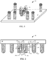
- FIG. 1 shows a perspective view of an example embodiment 10 of an IC, modified for a space efficient FC joint design.
- a substrate 12 such as a printed circuit board, a semiconductor substrate or an IC, is subsequently processed to include a first pillar 14.
- the first pillar 14 has a cylindrical shape with a circular cross-sectional end attached to the substrate 12.
- the example embodiment 10 further includes second pillars 16a, 16b, 16c and 16d (generally 16) surrounding the first pillar 14 and being taller than the first pillar 14.
- the second pillars 16 each have a rectangular shape with a rectangular cross-sectional end attached to the substrate 12.
- the number of second pillars 16 surrounding the first pillar 14 is 1, 2, 4, 6 or 8.
- the number of second pillars 16 surrounding the first pillar 14 is any even or odd number up to a practical manufacturing limit defined by the cross-sectional areas of the first pillar 14 and the second pillar 16.
- a larger first pillar 14 will accommodate more second pillars 16.
- the second pillars 16 are symmetrically disposed around the first pillar 14.
- the first pillar 14 and the second pillars 16 have shapes that differ from cylindrical and rectangular respectively, limited by the ability to efficiently surround the first pillar 14 with the second pillars 16 and to match the pillar structures to a corresponding assembly substrate.
- the second pillars 16 surrounding a first pillar 14 is a combination of alternative shapes and/or cross-sections.
- the substrate 12 includes the combination of the first pillar 14 and second pillars 16 as well as additional third pillars 18a to 18f (generally 18 or "tall cylindrical pillars").
- the signals generated or received at the substrate 12 are assigned to pillars based on requirements of current density or frequency characteristics (e.g., average or peak frequency components).
- a high frequency and/or high current signal will be electrically coupled to either the first pillar 14 or one of the third pillars 18, while a lower frequency and/or lower current density signal will use the more compact - lower solder volume second pillars 16.
- the formation of a group of signals defined by a first pillar 14 surrounded by one or more second pillars 16 is replicated uniformly across the substrate 12. In another embodiment, the formation of a group of signals defined by a first pillar 14 surrounded by one or more second pillars 16 is replicated only in areas of the substrate 12 based on signal requirements.
- FIG. 2 shows a side view of an example embodiment 20 similar to the embodiment 10 of FIG. 1 .
- each of the pillars 14, 16 and 18 have "attachment points" formed by solder deposited on the tip of the respective pillar, for example by an electroplating process.
- the first pillar 14 includes an attachment point22
- each of the third pillars 18 include a respective attachment point 24a to 24d (generally 24)
- each of the second pillars 16 include a respective attachment point 26a, 26b (not shown), 26c and 26d (not shown), (generally 26).
- the attachment points 22 and 24 are collinear with a central axis of the respective first pillar 14 and the third pillars 18, and on a respective end of each pillar.
- the attachment points 26 are on a side of the second pillars 16 facing the first pillar 14.
- the first pillar 14 has a diameter 30 being greater than the width 32 of each of the second pillars 16.
- a spacing 34 between a pair of attachment points 26 is wider than the diameter 30 and is also defined by a matching assembly substrate to which to embodiment 20 is subsequently attached.
- the first pillar 14 has a first length 40 measured between a first end 42 and a second end 44.
- the second pillars 16 each have a second length 50 measured between a third end 52 and a fourth end 54.
- the third pillars 18 each have a third length 60 measured between a fifth end 62 and a sixth end 64. In one embodiment, the third length 60 is the same as the second length 50.
- FIG. 3 through FIG. 17 show the progressive manufacturing steps used to form the embodiment 20 of FIG. 2 or similar example embodiments of the present disclosure.
- a substrate 70 includes a photoresist (PR) layer 72 deposited thereon.
- PR photoresist
- the PR layer 72 is patterned, developed and selectively stripped to form openings 74.
- the openings 74 are filled with a conductive material 76 used to form the pillars 14, 16 and 18 (e.g., Copper).
- an additional PR layer 78 is deposited, spun-on or otherwise applied.
- the PR layer 78 is developed and stripped to form an opening 80.
- PR photoresist
- an attachment point 82 (e.g., solder) fills the opening 80.
- a PR layer 84 is deposited and subsequently developed and stripped to form openings 86.
- additional conductive material 88 is added to file the openings 86 and thereby increase the height of resulting pillars.
- a PR layer 90 is deposited and subsequently developed and stripped to form openings 92.
- attachment points 94 (e.g., solder) fills the openings 92.
- openings 96 are formed.
- the openings 96 are filled with conductive material 98, thereby increasing a pillar height.
- openings 100 are formed in the PR.
- the openings 100 are filled with solder to form attachment points 102.
- the remaining PR 104 of FIG. 16 is removed, thereby forming a structure similar to the example embodiment 20 of FIG. 2 .
- FIG. 18 shows an example embodiment 110 of an assembly substrate forming a counterpart to an embodiment of a substrate with pillars, similar to that shown in FIGs. 1-2 .
- the embodiment 110 includes a substrate 112 with substrate pads 114a, 114b, 114c, 114d and 114e (generally 114).
- the substrate pads 114 of FIG. 18 are arranged so that a single substrate pad 114e will align with the first pillar 14.
- the plurality of substrate pads 114a, 114b, 114c and 114d will surround the central substrate pad 114e with a distance defined by the spacing 34 and to align with the second pillars 16.
- an area outside of the region 116 is subsequently modified through milling, drilling or the like, so that the attachment points 26a and 26c contact the remaining portions of the respective substrate pads 114a and 114c, while the attachment point 22 contacts the larger substrate pad 114e.
- a similar process occurs for the substrate pads 114b and 114d.
- the shape of the substrate pad 114e is correspondingly a hexagon or octagon so that that attachment points 26 of the second pillars 16 "face" the first pillar 14.
- a second cluster of substrate pads 118a to 118e defines a second grouping of substrate pads arranged to receive a group of a first pillar 14 surrounded by second pillars 16.
- the substrate pads 118 also have the defined region 116 similar to that used for subsequent milling of the substrate pads 114.
- one or more substrate pads 120a to 120r are placed as required on the substrate 112 to align with respective third pillars 18.
- FIG. 19 shows a cross-sectional view of FIG. 18 taken along A-A'.
- the example embodiment 130 of FIG. 19 includes a bottom section 132 and a top section 134 of the substrate 112 of FIG. 18 .
- the bottom section 132 includes a plurality of routing layers 136 and vias 138 defining circuit connections.
- Sections 140 and 142 define areas to be removed from the top section 134 (e.g., the area outside of the region 116 shown in FIG. 18 ). Removal of sections 140 and 142 is accomplished through a process that selectively removes the conductive material 114 (e.g., Copper) and insulation layers therebetween.
- Non-limiting examples of a process to remove the sections 140 and 142 include, but are not limited to, drilling, milling and chemical and/or ion etching.
- FIG. 20 shows an example embodiment 150 of a side view of FIG. 19 after removal of the sections 140 and 142.
- the substrate pads 114a and 114c (and similarly 114b and 114d) are modified with portions removed to form modified substrate pads 152 and 154 respectively.
- the resulting width 156 is designed to be the same as the spacing 34 between the attachment points 26a and 26c, shown in FIG. 2 .
- minor manufacturing variances between the width 156 ( FIG. 20 ) and the spacing 34 ( FIG. 2 ) are readily accommodated with the conformity of the solder used on the respective attachment points 26a and 26c.
- FIG. 21 shows a perspective view of an example embodiment 160 after the removal of sections 140 and 142 shown in FIG. 19 and FIG. 20 .
- An assembly substrate 162 includes one or more pad blocks 164 combined with one or more substrate pads 166.
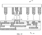
- FIG. 22 is an exploded view of an example embodiment 170 of An IC, (similar to FIG. 2 ) aligned for attachment to an example embodiment 180 of an assembly substrate, (similar to FIG. 20 ).
- attachment points 172, 174, 176 and 178 of respective third pillars are aligned to attach to the top of respective substrate pads 182, 184, 186 and 188.
- the attachment point 190 of a first pillar is aligned to attach to the top of a substrate pad 200.
- Attachment points 192 and 194 of respective second pillars are aligned to attach to the sides of respective substrate pads 202 and 204.
- the solder included in each attachment point 172, 174, 176, 178, 190, 192 and 194 is coated with flux.
- the flux is added to the solder by spraying, pin transfer or a combination of spraying and pin transfer.
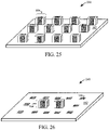
- FIGs. 23 to FIG. 26 show alternate embodiments to the example embodiment shown in FIG. 21 , where pad blocks 164 are placed at any desired location on the assembly substrate 162 in combination with substrate pads 166.
- FIG. 23 shows an example embodiment 210 of pad blocks 164 placed only at the periphery of the assembly substrate 162.
- FIG. 24 shows an example embodiment 220 of pad blocks 164 placed selectively at the periphery and at the core of the assembly substrate 162.
- FIG. 25 shows an example embodiment 230 of pad blocks 164 placed uniformly across the assembly substrate 162, with no substrate pads 166 present.
- FIG. 26 shows an example embodiment 240 of pad blocks 164 placed only at the core of the assembly substrate 162.
- an apparatus comprises an Integrated Circuit (IC), a first pillar and a second pillar.
- the first pillar comprises a first end and a second end.
- the first end is connected to the IC and the second end comprises a first attachment point collinear with a first central axis of the first pillar.
- the first attachment point comprises a first solder volume capacity.
- the second pillar comprises a third end and a fourth end.
- the third end is connected to the IC and the fourth end and comprises a second attachment point disposed on a side of the second pillar facing the first pillar, wherein the second attachment point comprises a second solder volume capacity being less than the first solder volume capacity.
- a first distance between the first end and the second end is less than a second distance between the third end and the fourth end.
- the second pillar may be one of a plurality of pillars, each disposed to surround the first pillar and comprising a respective attachment point facing the first pillar.
- Each of the plurality of pillars may be symmetrically disposed to surround the first pillar.
- the first pillar may comprise a cylindrical shape.
- the second pillar may comprise a rectangular shape.
- a first cross-sectional area of the first pillar may be greater than a second cross-sectional area of the second pillar.
- the first attachment point may be connected to a top facet of a pad block of an assembly substrate, the top facet parallel to the assembly substrate, and the second attachment point may be connected to a side facet of the pad block, the side facet orthogonal to the top facet.
- the IC and the assembly substrate may be encapsulated.
- an apparatus comprises a semiconductor substrate, a first pillar, a second pillar, and an assembly substrate.
- the first pillar comprises a first end and a second end.
- the first end is connected to the semiconductor substrate and the second end comprises a first attachment point collinear with a first central axis of the first pillar.
- the first attachment point comprises a first solder volume capacity.
- the second pillar comprises a third end and a fourth end.
- the third end is connected to the semiconductor substrate and the fourth end comprises a second attachment point disposed on a side of the second pillar facing the first pillar, wherein the second attachment point comprises a second solder volume capacity being less than the first solder volume capacity.
- the assembly substrate comprises a top facet and a side facet of a pad block, wherein the top facet is orthogonal to the side facet, the first attachment point is connected to the top facet and the second attachment point is connected to the side facet.
- the second pillar may be one of a plurality of pillars, each disposed to symmetrically surround the first pillar and comprising a respective attachment point facing the first pillar.
- the first pillar may comprise a cylindrical shape.
- the second pillar may comprise a rectangular shape.
- a first cross-sectional area of the first pillar may be greater than a second cross-sectional area of the second pillar.
- the semiconductor substrate and the assembly substrate may be encapsulated.
- an apparatus comprises a first substrate comprising a plurality of signal conductors, and a cylindrical pillar.
- the cylindrical pillar comprises a first end and a second end.
- the first end is connected to the first substrate and the second end comprises a first attachment point collinear with a first central axis of the cylindrical pillar.
- the first attachment point comprises a first solder volume capacity.
- a first one of a plurality of rectangular pillars is symmetrically disposed around the cylindrical pillar, the first rectangular pillar comprising a third end and a fourth end.
- the third end is connected to the first substrate and the fourth end comprises a second attachment point disposed on a side of the first rectangular pillar facing the cylindrical pillar, wherein the second attachment point comprises a second solder volume capacity being less than the first solder volume capacity.
- a first distance between the first end and the second end is less than a second distance between the third end and the fourth end.
- a second substrate comprises a top facet and a side facet of a pad block, wherein the top facet is orthogonal to the side facet, the first attachment point is connected to the top facet and the second attachment point is connected to the side facet.
- One of the signal conductors may comprise a high current density is electrically coupled to the cylindrical pillar and another one of the signal conductors comprising a low current density, lower than the high current density, is electrically coupled to one of the rectangular pillars.
- a first cross-sectional area of the cylindrical pillar may be greater than a second cross-sectional area of the first rectangular pillar.
- the plurality of rectangular pillars may comprise one of four, six or eight pillars.
- the first substrate further may comprise a tall cylindrical pillar comprising a fifth end, a sixth end and the second distance therebetween.
- the first substrate may comprise a plurality of the cylindrical pillars and a plurality of the tall cylindrical pillars.
Landscapes
- Wire Bonding (AREA)
- Physics & Mathematics (AREA)
- Geometry (AREA)
- Combinations Of Printed Boards (AREA)
Abstract

Description
- This disclosure relates generally to Flip Chip (FC) assembly, and more specifically to improving the density of a flip chip assembly with a combination of signal specific pillars.
- Integrated circuits with a large number of external connections or "pins" are often limited in their ability to be assembled into small packages with traditional wire bonding techniques. The sizes of these packages are deemed to be pin-limited rather than die-size limited. Accordingly, FC assemblies are often used for high Input/Output (I/O) IC devices. FC assemblies enable a high density of joints (e.g., solder joints), with low pitch distances. System on Chip (SoC) devices integrate additional functionality, thereby increasing the need to provide more I/O on the IC. One approach to increasing package I/O density is to reduce the diameter of a pillar connecting a semiconductor IC to the package substrate, however this approach is to the detriment of signal quality and/or current capacity.
- The present invention is illustrated by way of example and is not limited by the accompanying figures, in which like references indicate similar elements. Elements in the figures are illustrated for simplicity and clarity and have not necessarily been drawn to scale.
-
FIG. 1 is a perspective view of an Integrated Circuit (IC), modified for a space efficient flip chip joint design, in accordance with an example embodiment of the present disclosure. -
FIG. 2 is a side view of the IC ofFIG. 1 , in accordance with an example embodiment of the present disclosure. -
FIG. 3 through FIG. 17 are cross-sectional views of the progressive manufacturing steps a flip chip substrate, in accordance with an example embodiment of the present disclosure. -
FIG. 18 is a plan view of an example embodiment of an assembly substrate. -
FIG. 19 is a cross-sectional view of the example embodiment ofFIG. 18 taken along A-A', further illustrating the assembly substrate. -
FIG. 20 is a side view of the example embodiment ofFIG. 19 after removing a portion of a top layer. -
FIG. 21 is a perspective view of the example embodiment ofFIG. 20 -
FIG. 22 is an exploded view showing a coupling of the IC ofFIG. 2 to the assembly substrate ofFIG. 20 , in accordance with an example embodiment of the present disclosure. -
FIG. 23 through 26 are example embodiments of assembly substrates prepared for space efficient flip chip assembly. - Embodiments described herein provide for improvements in pin limited FC package density by using different pillar designs dependent upon electrical signal categories. Pillars having a small cross-sectional area support less solder volume than pillars with a larger cross-sectional area. Throughout this disclosure, references to low solder volume pillars and high solder volume pillars refer to pillars with different cross-sectional areas having correspondingly different capacities to support a volume of solder. In various embodiments, the solder is used in attachment points between the pillars and a substrate, to which the pillars are subsequently attached. High solder volume pillars are used for signals requiring high current density or having high signal frequencies, while low solder volume pillars are used for signals having lower current density or lower signal frequencies. The low solder volume pillars are smaller than the high solder volume pillars, thus improving package density. Specifically, in one embodiment, cylindrical pillars are used for high solder volume connections between the semiconductor and package substrate, while rectangular pillars are used for signals that can tolerate a lower solder volume. One or more rectangular pillars are disposed around a shorter cylindrical pillar. The cylindrical pillar is soldered to a matching assembly substrate through a vertical connection, orthogonal to a surface of the semiconductor, while the one or more rectangular pillars are connected horizontally to the assembly substrate, or parallel to the surface of the semiconductor.
-
FIG. 1 shows a perspective view of anexample embodiment 10 of an IC, modified for a space efficient FC joint design. Asubstrate 12, such as a printed circuit board, a semiconductor substrate or an IC, is subsequently processed to include afirst pillar 14. In one embodiment, thefirst pillar 14 has a cylindrical shape with a circular cross-sectional end attached to thesubstrate 12. Theexample embodiment 10 further includessecond pillars first pillar 14 and being taller than thefirst pillar 14. In one example embodiment, the second pillars 16 each have a rectangular shape with a rectangular cross-sectional end attached to thesubstrate 12. In other embodiments, the number of second pillars 16 surrounding thefirst pillar 14 is 1, 2, 4, 6 or 8. In another embodiment, the number of second pillars 16 surrounding thefirst pillar 14 is any even or odd number up to a practical manufacturing limit defined by the cross-sectional areas of thefirst pillar 14 and the second pillar 16. For example, a largerfirst pillar 14 will accommodate more second pillars 16. In one embodiment, the second pillars 16 are symmetrically disposed around thefirst pillar 14. In other example embodiments thefirst pillar 14 and the second pillars 16 have shapes that differ from cylindrical and rectangular respectively, limited by the ability to efficiently surround thefirst pillar 14 with the second pillars 16 and to match the pillar structures to a corresponding assembly substrate. Similarly, in one embodiment, the second pillars 16 surrounding afirst pillar 14 is a combination of alternative shapes and/or cross-sections. - In the
example embodiment 10, thesubstrate 12 includes the combination of thefirst pillar 14 and second pillars 16 as well as additionalthird pillars 18a to 18f (generally 18 or "tall cylindrical pillars"). In example embodiments, the signals generated or received at thesubstrate 12 are assigned to pillars based on requirements of current density or frequency characteristics (e.g., average or peak frequency components). In one example, a high frequency and/or high current signal will be electrically coupled to either thefirst pillar 14 or one of the third pillars 18, while a lower frequency and/or lower current density signal will use the more compact - lower solder volume second pillars 16. In one embodiment, the formation of a group of signals defined by afirst pillar 14 surrounded by one or more second pillars 16 is replicated uniformly across thesubstrate 12. In another embodiment, the formation of a group of signals defined by afirst pillar 14 surrounded by one or more second pillars 16 is replicated only in areas of thesubstrate 12 based on signal requirements. -
FIG. 2 shows a side view of anexample embodiment 20 similar to theembodiment 10 ofFIG. 1 . In theembodiment 20, each of thepillars 14, 16 and 18 have "attachment points" formed by solder deposited on the tip of the respective pillar, for example by an electroplating process. Specifically, thefirst pillar 14 includes an attachment point22, each of the third pillars 18 include a respective attachment point 24a to 24d (generally 24), and each of the second pillars 16 include arespective attachment point 26a, 26b (not shown), 26c and 26d (not shown), (generally 26). Theattachment points 22 and 24 are collinear with a central axis of the respectivefirst pillar 14 and the third pillars 18, and on a respective end of each pillar. Conversely, the attachment points 26 are on a side of the second pillars 16 facing thefirst pillar 14. In theexample embodiment 20, thefirst pillar 14 has adiameter 30 being greater than thewidth 32 of each of the second pillars 16. Aspacing 34 between a pair of attachment points 26 is wider than thediameter 30 and is also defined by a matching assembly substrate to which toembodiment 20 is subsequently attached. Thefirst pillar 14 has afirst length 40 measured between afirst end 42 and asecond end 44. The second pillars 16 each have asecond length 50 measured between athird end 52 and afourth end 54. The third pillars 18 each have athird length 60 measured between a fifth end 62 and asixth end 64. In one embodiment, thethird length 60 is the same as thesecond length 50. During the assembly process of attaching theembodiment 20 to a corresponding assembly substrate, small dimensional and shape variations are accommodated by deformation and flowing of the solder tips on respective attachment points. -
FIG. 3 through FIG. 17 , show the progressive manufacturing steps used to form theembodiment 20 ofFIG. 2 or similar example embodiments of the present disclosure. InFIG. 3 , asubstrate 70 includes a photoresist (PR)layer 72 deposited thereon. AtFIG. 4 , thePR layer 72 is patterned, developed and selectively stripped to form openings 74. AtFIG. 5 , the openings 74 are filled with a conductive material 76 used to form thepillars 14, 16 and 18 (e.g., Copper). AtFIG. 6 , anadditional PR layer 78 is deposited, spun-on or otherwise applied. AtFIG. 7 , thePR layer 78 is developed and stripped to form anopening 80. AtFIG. 8 , an attachment point 82 (e.g., solder) fills theopening 80. AtFIG. 9 , aPR layer 84 is deposited and subsequently developed and stripped to form openings 86. AtFIG. 10 , additionalconductive material 88 is added to file the openings 86 and thereby increase the height of resulting pillars. AtFIG. 11 , aPR layer 90 is deposited and subsequently developed and stripped to form openings 92. AtFIG. 12 , attachment points 94 (e.g., solder) fills the openings 92. AtFIG. 13 ,openings 96 are formed. AtFIG. 14 , theopenings 96 are filled withconductive material 98, thereby increasing a pillar height. AtFIG. 15 ,openings 100 are formed in the PR. AtFIG. 16 , theopenings 100 are filled with solder to form attachment points 102. AtFIG. 17 , the remainingPR 104 ofFIG. 16 is removed, thereby forming a structure similar to theexample embodiment 20 ofFIG. 2 . -
FIG. 18 shows anexample embodiment 110 of an assembly substrate forming a counterpart to an embodiment of a substrate with pillars, similar to that shown inFIGs. 1-2 . Theembodiment 110 includes asubstrate 112 withsubstrate pads FIG. 1 and FIG. 2 , in one embodiment the substrate pads 114 ofFIG. 18 are arranged so that asingle substrate pad 114e will align with thefirst pillar 14. The plurality ofsubstrate pads central substrate pad 114e with a distance defined by thespacing 34 and to align with the second pillars 16. Specifically, an area outside of theregion 116 is subsequently modified through milling, drilling or the like, so that the attachment points 26a and 26c contact the remaining portions of therespective substrate pads attachment point 22 contacts thelarger substrate pad 114e. A similar process occurs for thesubstrate pads 114b and 114d. In alternate embodiments, having 6 or 8 second pillars 16, the shape of thesubstrate pad 114e is correspondingly a hexagon or octagon so that that attachment points 26 of the second pillars 16 "face" thefirst pillar 14. As shown in theexample embodiment 110, a second cluster ofsubstrate pads 118a to 118e (generally 118) defines a second grouping of substrate pads arranged to receive a group of afirst pillar 14 surrounded by second pillars 16. The substrate pads 118 also have the definedregion 116 similar to that used for subsequent milling of the substrate pads 114. In addition to the combination offirst pillars 14 and second pillars 16, one ormore substrate pads 120a to 120r (generally 120) are placed as required on thesubstrate 112 to align with respective third pillars 18. -
FIG. 19 shows a cross-sectional view ofFIG. 18 taken along A-A'. Theexample embodiment 130 ofFIG. 19 includes abottom section 132 and atop section 134 of thesubstrate 112 ofFIG. 18 . Thebottom section 132 includes a plurality of routinglayers 136 and vias 138 defining circuit connections.Sections region 116 shown inFIG. 18 ). Removal ofsections sections -
FIG. 20 shows anexample embodiment 150 of a side view ofFIG. 19 after removal of thesections FIG. 19 , thesubstrate pads substrate pads width 156 is designed to be the same as the spacing 34 between the attachment points 26a and 26c, shown inFIG. 2 . As previously discussed, minor manufacturing variances between the width 156 (FIG. 20 ) and the spacing 34 (FIG. 2 ) are readily accommodated with the conformity of the solder used on therespective attachment points FIG. 21 shows a perspective view of anexample embodiment 160 after the removal ofsections FIG. 19 andFIG. 20 . Anassembly substrate 162 includes one or more pad blocks 164 combined with one ormore substrate pads 166. -
FIG. 22 is an exploded view of anexample embodiment 170 of An IC, (similar toFIG. 2 ) aligned for attachment to anexample embodiment 180 of an assembly substrate, (similar toFIG. 20 ). Specifically, attachment points 172, 174, 176 and 178 of respective third pillars are aligned to attach to the top ofrespective substrate pads attachment point 190 of a first pillar is aligned to attach to the top of asubstrate pad 200. Attachment points 192 and 194 of respective second pillars are aligned to attach to the sides ofrespective substrate pads embodiments attachment point -
FIGs. 23 to FIG. 26 show alternate embodiments to the example embodiment shown inFIG. 21 , where pad blocks 164 are placed at any desired location on theassembly substrate 162 in combination withsubstrate pads 166. Specifically,FIG. 23 shows anexample embodiment 210 of pad blocks 164 placed only at the periphery of theassembly substrate 162.FIG. 24 shows anexample embodiment 220 of pad blocks 164 placed selectively at the periphery and at the core of theassembly substrate 162.FIG. 25 shows anexample embodiment 230 of pad blocks 164 placed uniformly across theassembly substrate 162, with nosubstrate pads 166 present.FIG. 26 shows anexample embodiment 240 of pad blocks 164 placed only at the core of theassembly substrate 162. - As will be appreciated, embodiments as disclosed include at least the following. In one embodiment, an apparatus comprises an Integrated Circuit (IC), a first pillar and a second pillar. The first pillar comprises a first end and a second end. The first end is connected to the IC and the second end comprises a first attachment point collinear with a first central axis of the first pillar. The first attachment point comprises a first solder volume capacity. The second pillar comprises a third end and a fourth end. The third end is connected to the IC and the fourth end and comprises a second attachment point disposed on a side of the second pillar facing the first pillar, wherein the second attachment point comprises a second solder volume capacity being less than the first solder volume capacity. A first distance between the first end and the second end is less than a second distance between the third end and the fourth end.
- Alternative embodiments of the apparatus include one of the following features, or any combination thereof. The second pillar may be one of a plurality of pillars, each disposed to surround the first pillar and comprising a respective attachment point facing the first pillar. Each of the plurality of pillars may be symmetrically disposed to surround the first pillar. The first pillar may comprise a cylindrical shape. The second pillar may comprise a rectangular shape. A first cross-sectional area of the first pillar may be greater than a second cross-sectional area of the second pillar. The first attachment point may be connected to a top facet of a pad block of an assembly substrate, the top facet parallel to the assembly substrate, and the second attachment point may be connected to a side facet of the pad block, the side facet orthogonal to the top facet. The IC and the assembly substrate may be encapsulated.
- In another embodiment, an apparatus comprises a semiconductor substrate, a first pillar, a second pillar, and an assembly substrate. the first pillar comprises a first end and a second end. The first end is connected to the semiconductor substrate and the second end comprises a first attachment point collinear with a first central axis of the first pillar. The first attachment point comprises a first solder volume capacity. The second pillar comprises a third end and a fourth end. The third end is connected to the semiconductor substrate and the fourth end comprises a second attachment point disposed on a side of the second pillar facing the first pillar, wherein the second attachment point comprises a second solder volume capacity being less than the first solder volume capacity. A first distance between the first end and the second end is less than a second distance between the third end and the fourth end. The assembly substrate comprises a top facet and a side facet of a pad block, wherein the top facet is orthogonal to the side facet, the first attachment point is connected to the top facet and the second attachment point is connected to the side facet.
- Alternative embodiments of the apparatus include one of the following features, or any combination thereof. The second pillar may be one of a plurality of pillars, each disposed to symmetrically surround the first pillar and comprising a respective attachment point facing the first pillar. The first pillar may comprise a cylindrical shape. The second pillar may comprise a rectangular shape. A first cross-sectional area of the first pillar may be greater than a second cross-sectional area of the second pillar. The semiconductor substrate and the assembly substrate may be encapsulated.
- In another embodiment, an apparatus comprises a first substrate comprising a plurality of signal conductors, and a cylindrical pillar. The cylindrical pillar comprises a first end and a second end. The first end is connected to the first substrate and the second end comprises a first attachment point collinear with a first central axis of the cylindrical pillar. The first attachment point comprises a first solder volume capacity. A first one of a plurality of rectangular pillars is symmetrically disposed around the cylindrical pillar, the first rectangular pillar comprising a third end and a fourth end. The third end is connected to the first substrate and the fourth end comprises a second attachment point disposed on a side of the first rectangular pillar facing the cylindrical pillar, wherein the second attachment point comprises a second solder volume capacity being less than the first solder volume capacity. A first distance between the first end and the second end is less than a second distance between the third end and the fourth end. A second substrate comprises a top facet and a side facet of a pad block, wherein the top facet is orthogonal to the side facet, the first attachment point is connected to the top facet and the second attachment point is connected to the side facet.
- Alternative embodiments of the apparatus include one of the following features, or any combination thereof. One of the signal conductors may comprise a high current density is electrically coupled to the cylindrical pillar and another one of the signal conductors comprising a low current density, lower than the high current density, is electrically coupled to one of the rectangular pillars. A first cross-sectional area of the cylindrical pillar may be greater than a second cross-sectional area of the first rectangular pillar. The plurality of rectangular pillars may comprise one of four, six or eight pillars. The first substrate further may comprise a tall cylindrical pillar comprising a fifth end, a sixth end and the second distance therebetween. The first substrate may comprise a plurality of the cylindrical pillars and a plurality of the tall cylindrical pillars.
- Although the invention is described herein with reference to specific embodiments, various modifications and changes can be made without departing from the scope of the present invention as set forth in the claims below. Accordingly, the specification and figures are to be regarded in an illustrative rather than a restrictive sense, and all such modifications are intended to be included within the scope of the present invention. Any benefits, advantages, or solutions to problems that are described herein with regard to specific embodiments are not intended to be construed as a critical, required, or essential feature or element of any or all the claims.
- Unless stated otherwise, terms such as "first" and "second" are used to arbitrarily distinguish between the elements such terms describe. Thus, these terms are not necessarily intended to indicate temporal or other prioritization of such elements.
Claims (15)
- An apparatus comprising:
an Integrated Circuit (IC) and/or a semiconductor substrate;the apparatus further comprising:
a first pillar comprising a first end and a second end, the first end connected to the IC and/or the semiconductor substrate, wherein the second end comprising a first attachment point collinear with a first central axis of the first pillar, wherein the first attachment point comprises a first solder volume capacity; anda second pillar comprising a third end and a fourth end, the third end connected to the IC and/or the semiconductor substrate, wherein the fourth end comprising a second attachment point disposed on a side of the second pillar facing the first pillar, wherein the second attachment point comprises a second solder volume capacity being less than the first solder volume capacity, and a first distance between the first end and the second end is less than a second distance between the third end and the fourth end. - The apparatus of claim 1 wherein the second pillar is one of a plurality of pillars, each disposed to surround the first pillar and comprising a respective attachment point facing the first pillar.
- The apparatus of claim 2 wherein each of the plurality of pillars are symmetrically disposed to surround the first pillar.
- The apparatus of any of claims 1 to 3, wherein the first pillar comprises a cylindrical shape.
- The apparatus of any of claims 1 to 4, wherein the second pillar comprises a rectangular shape.
- The apparatus of any of claims 1 to 5, wherein a first cross-sectional area of the first pillar is greater than a second cross-sectional area of the second pillar.
- The apparatus of any of claims 1 to 6, further comprising connecting the first attachment point to a top facet of a pad block of an assembly substrate, the top facet parallel to the assembly substrate, and connecting the second attachment point to a side facet of the pad block, the side facet orthogonal to the top facet.
- The apparatus of claim 7 wherein, if the apparatus comprising the IC, the IC and the assembly substrate are encapsulated.
- The apparatus of any of claims 1 to 6, wherein, if the apparatus comprising the semiconductor substrate, the apparatus further comprising an assembly substrate comprising a top facet and a side facet of a pad block, wherein the top facet is orthogonal to the side facet, the first attachment point connected to the top facet and the second attachment point connected to the side facet.
- An apparatus comprising:a first substrate comprising a plurality of signal conductors;a cylindrical pillar comprising a first end and a second end, the first end connected to the first substrate and the second end comprising a first attachment point collinear with a first central axis of the cylindrical pillar, wherein the first attachment point comprises a first solder volume capacity;a first one of a plurality of rectangular pillars symmetrically disposed around the cylindrical pillar, the first rectangular pillar comprising a third end and a fourth end, the third end connected to the first substrate and the fourth end comprising a second attachment point disposed on a side of the first rectangular pillar facing the cylindrical pillar, wherein the second attachment point comprises a second solder volume capacity being less than the first solder volume capacity, and a first distance between the first end and the second end is less than a second distance between the third end and the fourth end; anda second substrate comprising a top facet and a side facet of a pad block,wherein the top facet is orthogonal to the side facet, the first attachment point connected to the top facet and the second attachment point connected to the side facet.
- The apparatus of claim 10, wherein one of the signal conductors comprising a high current density is electrically coupled to the cylindrical pillar and another one of the signal conductors comprising a low current density, lower than the high current density, is electrically coupled to one of the rectangular pillars.
- The apparatus of any of claims 10 to 11, wherein a first cross-sectional area of the cylindrical pillar is greater than a second cross-sectional area of the first rectangular pillar.
- The apparatus of any of claims 10 to 12, wherein the plurality of rectangular pillars comprises one of four, six or eight pillars.
- The apparatus of any of claims 10 to 13, wherein the first substrate further comprises a tall cylindrical pillar comprising a fifth end, a sixth end and the second distance therebetween.
- The apparatus of claim 14 wherein the first substrate comprises a plurality of the cylindrical pillars and a plurality of the tall cylindrical pillars.
Applications Claiming Priority (1)
| Application Number | Priority Date | Filing Date | Title |
|---|---|---|---|
| US17/376,053 US11521947B1 (en) | 2021-07-14 | 2021-07-14 | Space efficient flip chip joint design |
Publications (3)
| Publication Number | Publication Date |
|---|---|
| EP4120339A2 true EP4120339A2 (en) | 2023-01-18 |
| EP4120339A3 EP4120339A3 (en) | 2023-07-26 |
| EP4120339B1 EP4120339B1 (en) | 2025-05-07 |
Family
ID=83006168
Family Applications (1)
| Application Number | Title | Priority Date | Filing Date |
|---|---|---|---|
| EP22182373.5A Active EP4120339B1 (en) | 2021-07-14 | 2022-06-30 | Space efficient flip chip joint design using different pillar designs |
Country Status (2)
| Country | Link |
|---|---|
| US (1) | US11521947B1 (en) |
| EP (1) | EP4120339B1 (en) |
Families Citing this family (1)
| Publication number | Priority date | Publication date | Assignee | Title |
|---|---|---|---|---|
| CN113594119B (en) * | 2021-06-25 | 2024-05-14 | 苏州汉天下电子有限公司 | Semiconductor package and method of manufacturing the same |
Family Cites Families (16)
| Publication number | Priority date | Publication date | Assignee | Title |
|---|---|---|---|---|
| US7344915B2 (en) * | 2005-03-14 | 2008-03-18 | Advanced Semiconductor Engineering, Inc. | Method for manufacturing a semiconductor package with a laminated chip cavity |
| IL175011A (en) * | 2006-04-20 | 2011-09-27 | Amitech Ltd | Coreless cavity substrates for chip packaging and their fabrication |
| US7727816B2 (en) * | 2006-07-21 | 2010-06-01 | Stats Chippac Ltd. | Integrated circuit package system with offset stacked die |
| US7618848B2 (en) * | 2006-08-09 | 2009-11-17 | Stats Chippac Ltd. | Integrated circuit package system with supported stacked die |
| US7635914B2 (en) * | 2007-05-17 | 2009-12-22 | Texas Instruments Incorporated | Multi layer low cost cavity substrate fabrication for pop packages |
| WO2008154450A1 (en) * | 2007-06-08 | 2008-12-18 | Valentx, Inc. | Methods and devices for intragastric support of functional or prosthetic gastrointestinal devices |
| US8853558B2 (en) * | 2010-12-10 | 2014-10-07 | Tessera, Inc. | Interconnect structure |
| US9806045B2 (en) * | 2013-08-29 | 2017-10-31 | Taiwan Semiconductor Manufacturing Company Ltd. | Interconnection structure including a metal post encapsulated by solder joint having a concave outer surface |
| KR20150136393A (en) * | 2014-05-27 | 2015-12-07 | 에스케이하이닉스 주식회사 | Flip chip package having chip fixing structure |
| US9305877B1 (en) * | 2014-10-30 | 2016-04-05 | Taiwan Semiconductor Manufacturing Company, Ltd. | 3D package with through substrate vias |
| US10283480B2 (en) * | 2015-08-06 | 2019-05-07 | Qorvo Us, Inc. | Substrate structure with selective surface finishes for flip chip assembly |
| EP4299803A3 (en) * | 2016-05-02 | 2024-03-27 | Encodia, Inc. | Macromolecule analysis employing nucleic acid encoding |
| US10254499B1 (en) * | 2016-08-05 | 2019-04-09 | Southern Methodist University | Additive manufacturing of active devices using dielectric, conductive and magnetic materials |
| DE102018122228B4 (en) * | 2017-11-15 | 2023-01-26 | Taiwan Semiconductor Manufacturing Company, Ltd. | Integrated multichip fan-out package and method for its manufacture |
| KR102791221B1 (en) * | 2019-01-31 | 2025-04-07 | 에스케이하이닉스 주식회사 | semiconductor package having anchor structure |
| AU2020361681A1 (en) * | 2019-10-10 | 2022-05-05 | 1859, Inc. | Methods and systems for microfluidic screening |
-
2021
- 2021-07-14 US US17/376,053 patent/US11521947B1/en active Active
-
2022
- 2022-06-30 EP EP22182373.5A patent/EP4120339B1/en active Active
Also Published As
| Publication number | Publication date |
|---|---|
| EP4120339A3 (en) | 2023-07-26 |
| EP4120339B1 (en) | 2025-05-07 |
| US11521947B1 (en) | 2022-12-06 |
Similar Documents
| Publication | Publication Date | Title |
|---|---|---|
| US10460958B2 (en) | Method of manufacturing embedded packaging with preformed vias | |
| US6512175B2 (en) | Electronic packaging device | |
| KR20130086347A (en) | Stackable molded microelectronic packages with area array unit connectors | |
| KR20080040039A (en) | Interconnect substrates for microelectronic dies, methods of forming vias in such substrates, and methods of packaging microelectronic devices | |
| US6528871B1 (en) | Structure and method for mounting semiconductor devices | |
| EP2482311A2 (en) | Semiconductor device, method of manufacturing semiconductor device, and electronic device | |
| US5382759A (en) | Massive parallel interconnection attachment using flexible circuit | |
| EP1665379B1 (en) | Electronic package having a folded flexible substrate and method of manufacturing the same | |
| CN1568543B (en) | semiconductor element | |
| US5917235A (en) | Semiconductor device having LOC structure, a semiconductor device lead frame, TAB leads, and an insulating TAB tape | |
| EP4120339B1 (en) | Space efficient flip chip joint design using different pillar designs | |
| US7131850B2 (en) | Socket for a microelectronic component having reduced electrical resistance and inductance | |
| US6627986B2 (en) | Substrate for semiconductor device and semiconductor device fabrication using the same | |
| US12381139B2 (en) | Electronic device and multilevel package substrate with elevated trace features for solder and/or die confinement and method for fabricating the electronic device | |
| KR20010104147A (en) | Multiple line grid and fabrication method thereof and method for mounting semiconductor chip on pcb board by using it | |
| JP2007266492A (en) | Package substrate manufacturing method and package substrate | |
| JP2001237346A (en) | Semiconductor element mounting substrate and method of manufacturing semiconductor device | |
| US12191362B2 (en) | Stacked semiconductor devices in sealants and interconnected with pillar electrodes | |
| KR20010105285A (en) | Semiconductor circuit device and method for manufacturing thereof | |
| US9832887B2 (en) | Micro mechanical anchor for 3D architecture | |
| JP2002246552A (en) | Semiconductor device | |
| EP1049163A1 (en) | Multiple line grid array package and a method for the manufacture thereof | |
| KR20030094695A (en) | Stacking type semiconductor connector, semiconductor package therewith and manufacturing method thereof | |
| KR20040047248A (en) | Multiple line grid and high end semiconductor package by using it | |
| HK1084506B (en) | Electronic package having a folded flexible substrate and method of manufacturing the same |
Legal Events
| Date | Code | Title | Description |
|---|---|---|---|
| PUAI | Public reference made under article 153(3) epc to a published international application that has entered the european phase |
Free format text: ORIGINAL CODE: 0009012 |
|
| STAA | Information on the status of an ep patent application or granted ep patent |
Free format text: STATUS: THE APPLICATION HAS BEEN PUBLISHED |
|
| AK | Designated contracting states |
Kind code of ref document: A2 Designated state(s): AL AT BE BG CH CY CZ DE DK EE ES FI FR GB GR HR HU IE IS IT LI LT LU LV MC MK MT NL NO PL PT RO RS SE SI SK SM TR |
|
| REG | Reference to a national code |
Ref legal event code: R079 Free format text: PREVIOUS MAIN CLASS: H01L0023485000 Ref country code: DE Ref legal event code: R079 Ref document number: 602022014134 Country of ref document: DE Free format text: PREVIOUS MAIN CLASS: H01L0023485000 Ipc: H01L0023000000 |
|
| PUAL | Search report despatched |
Free format text: ORIGINAL CODE: 0009013 |
|
| AK | Designated contracting states |
Kind code of ref document: A3 Designated state(s): AL AT BE BG CH CY CZ DE DK EE ES FI FR GB GR HR HU IE IS IT LI LT LU LV MC MK MT NL NO PL PT RO RS SE SI SK SM TR |
|
| RIC1 | Information provided on ipc code assigned before grant |
Ipc: H01L 23/498 20060101ALI20230621BHEP Ipc: H01L 23/00 20060101AFI20230621BHEP |
|
| STAA | Information on the status of an ep patent application or granted ep patent |
Free format text: STATUS: REQUEST FOR EXAMINATION WAS MADE |
|
| 17P | Request for examination filed |
Effective date: 20240126 |
|
| RBV | Designated contracting states (corrected) |
Designated state(s): AL AT BE BG CH CY CZ DE DK EE ES FI FR GB GR HR HU IE IS IT LI LT LU LV MC MK MT NL NO PL PT RO RS SE SI SK SM TR |
|
| GRAP | Despatch of communication of intention to grant a patent |
Free format text: ORIGINAL CODE: EPIDOSNIGR1 |
|
| STAA | Information on the status of an ep patent application or granted ep patent |
Free format text: STATUS: GRANT OF PATENT IS INTENDED |
|
| INTG | Intention to grant announced |
Effective date: 20250217 |
|
| GRAS | Grant fee paid |
Free format text: ORIGINAL CODE: EPIDOSNIGR3 |
|
| GRAA | (expected) grant |
Free format text: ORIGINAL CODE: 0009210 |
|
| STAA | Information on the status of an ep patent application or granted ep patent |
Free format text: STATUS: THE PATENT HAS BEEN GRANTED |
|
| AK | Designated contracting states |
Kind code of ref document: B1 Designated state(s): AL AT BE BG CH CY CZ DE DK EE ES FI FR GB GR HR HU IE IS IT LI LT LU LV MC MK MT NL NO PL PT RO RS SE SI SK SM TR |
|
| REG | Reference to a national code |
Ref country code: GB Ref legal event code: FG4D |
|
| REG | Reference to a national code |
Ref country code: CH Ref legal event code: EP |
|
| REG | Reference to a national code |
Ref country code: DE Ref legal event code: R096 Ref document number: 602022014134 Country of ref document: DE |
|
| REG | Reference to a national code |
Ref country code: IE Ref legal event code: FG4D |
|
| PGFP | Annual fee paid to national office [announced via postgrant information from national office to epo] |
Ref country code: DE Payment date: 20250520 Year of fee payment: 4 |
|
| REG | Reference to a national code |
Ref country code: NL Ref legal event code: MP Effective date: 20250507 |
|
| PG25 | Lapsed in a contracting state [announced via postgrant information from national office to epo] |
Ref country code: PT Free format text: LAPSE BECAUSE OF FAILURE TO SUBMIT A TRANSLATION OF THE DESCRIPTION OR TO PAY THE FEE WITHIN THE PRESCRIBED TIME-LIMIT Effective date: 20250908 Ref country code: FI Free format text: LAPSE BECAUSE OF FAILURE TO SUBMIT A TRANSLATION OF THE DESCRIPTION OR TO PAY THE FEE WITHIN THE PRESCRIBED TIME-LIMIT Effective date: 20250507 Ref country code: ES Free format text: LAPSE BECAUSE OF FAILURE TO SUBMIT A TRANSLATION OF THE DESCRIPTION OR TO PAY THE FEE WITHIN THE PRESCRIBED TIME-LIMIT Effective date: 20250507 |
|
| REG | Reference to a national code |
Ref country code: LT Ref legal event code: MG9D |
|
| PG25 | Lapsed in a contracting state [announced via postgrant information from national office to epo] |
Ref country code: NO Free format text: LAPSE BECAUSE OF FAILURE TO SUBMIT A TRANSLATION OF THE DESCRIPTION OR TO PAY THE FEE WITHIN THE PRESCRIBED TIME-LIMIT Effective date: 20250807 Ref country code: GR Free format text: LAPSE BECAUSE OF FAILURE TO SUBMIT A TRANSLATION OF THE DESCRIPTION OR TO PAY THE FEE WITHIN THE PRESCRIBED TIME-LIMIT Effective date: 20250808 |
|
| PG25 | Lapsed in a contracting state [announced via postgrant information from national office to epo] |
Ref country code: NL Free format text: LAPSE BECAUSE OF FAILURE TO SUBMIT A TRANSLATION OF THE DESCRIPTION OR TO PAY THE FEE WITHIN THE PRESCRIBED TIME-LIMIT Effective date: 20250507 Ref country code: PL Free format text: LAPSE BECAUSE OF FAILURE TO SUBMIT A TRANSLATION OF THE DESCRIPTION OR TO PAY THE FEE WITHIN THE PRESCRIBED TIME-LIMIT Effective date: 20250507 |
|
| REG | Reference to a national code |
Ref country code: AT Ref legal event code: MK05 Ref document number: 1793465 Country of ref document: AT Kind code of ref document: T Effective date: 20250507 |
|
| PG25 | Lapsed in a contracting state [announced via postgrant information from national office to epo] |
Ref country code: BG Free format text: LAPSE BECAUSE OF FAILURE TO SUBMIT A TRANSLATION OF THE DESCRIPTION OR TO PAY THE FEE WITHIN THE PRESCRIBED TIME-LIMIT Effective date: 20250507 |
|
| PG25 | Lapsed in a contracting state [announced via postgrant information from national office to epo] |
Ref country code: HR Free format text: LAPSE BECAUSE OF FAILURE TO SUBMIT A TRANSLATION OF THE DESCRIPTION OR TO PAY THE FEE WITHIN THE PRESCRIBED TIME-LIMIT Effective date: 20250507 |
|
| PG25 | Lapsed in a contracting state [announced via postgrant information from national office to epo] |
Ref country code: AT Free format text: LAPSE BECAUSE OF FAILURE TO SUBMIT A TRANSLATION OF THE DESCRIPTION OR TO PAY THE FEE WITHIN THE PRESCRIBED TIME-LIMIT Effective date: 20250507 |
|
| PG25 | Lapsed in a contracting state [announced via postgrant information from national office to epo] |
Ref country code: RS Free format text: LAPSE BECAUSE OF FAILURE TO SUBMIT A TRANSLATION OF THE DESCRIPTION OR TO PAY THE FEE WITHIN THE PRESCRIBED TIME-LIMIT Effective date: 20250807 |
|
| PG25 | Lapsed in a contracting state [announced via postgrant information from national office to epo] |
Ref country code: IS Free format text: LAPSE BECAUSE OF FAILURE TO SUBMIT A TRANSLATION OF THE DESCRIPTION OR TO PAY THE FEE WITHIN THE PRESCRIBED TIME-LIMIT Effective date: 20250907 |
|
| PG25 | Lapsed in a contracting state [announced via postgrant information from national office to epo] |
Ref country code: LV Free format text: LAPSE BECAUSE OF FAILURE TO SUBMIT A TRANSLATION OF THE DESCRIPTION OR TO PAY THE FEE WITHIN THE PRESCRIBED TIME-LIMIT Effective date: 20250507 |
|
| REG | Reference to a national code |
Ref country code: DE Ref legal event code: R079 Ref document number: 602022014134 Country of ref document: DE Free format text: PREVIOUS MAIN CLASS: H01L0023000000 Ipc: H10W0099000000 |
|
| PG25 | Lapsed in a contracting state [announced via postgrant information from national office to epo] |
Ref country code: DK Free format text: LAPSE BECAUSE OF FAILURE TO SUBMIT A TRANSLATION OF THE DESCRIPTION OR TO PAY THE FEE WITHIN THE PRESCRIBED TIME-LIMIT Effective date: 20250507 Ref country code: SM Free format text: LAPSE BECAUSE OF FAILURE TO SUBMIT A TRANSLATION OF THE DESCRIPTION OR TO PAY THE FEE WITHIN THE PRESCRIBED TIME-LIMIT Effective date: 20250507 |
|
| PG25 | Lapsed in a contracting state [announced via postgrant information from national office to epo] |
Ref country code: CZ Free format text: LAPSE BECAUSE OF FAILURE TO SUBMIT A TRANSLATION OF THE DESCRIPTION OR TO PAY THE FEE WITHIN THE PRESCRIBED TIME-LIMIT Effective date: 20250507 |
|
| PG25 | Lapsed in a contracting state [announced via postgrant information from national office to epo] |
Ref country code: EE Free format text: LAPSE BECAUSE OF FAILURE TO SUBMIT A TRANSLATION OF THE DESCRIPTION OR TO PAY THE FEE WITHIN THE PRESCRIBED TIME-LIMIT Effective date: 20250507 |
|
| PG25 | Lapsed in a contracting state [announced via postgrant information from national office to epo] |
Ref country code: SK Free format text: LAPSE BECAUSE OF FAILURE TO SUBMIT A TRANSLATION OF THE DESCRIPTION OR TO PAY THE FEE WITHIN THE PRESCRIBED TIME-LIMIT Effective date: 20250507 |
|
| REG | Reference to a national code |
Ref country code: CH Ref legal event code: H13 Free format text: ST27 STATUS EVENT CODE: U-0-0-H10-H13 (AS PROVIDED BY THE NATIONAL OFFICE) Effective date: 20260127 |
|
| PG25 | Lapsed in a contracting state [announced via postgrant information from national office to epo] |
Ref country code: IT Free format text: LAPSE BECAUSE OF FAILURE TO SUBMIT A TRANSLATION OF THE DESCRIPTION OR TO PAY THE FEE WITHIN THE PRESCRIBED TIME-LIMIT Effective date: 20250507 |
|
| PG25 | Lapsed in a contracting state [announced via postgrant information from national office to epo] |
Ref country code: RO Free format text: LAPSE BECAUSE OF FAILURE TO SUBMIT A TRANSLATION OF THE DESCRIPTION OR TO PAY THE FEE WITHIN THE PRESCRIBED TIME-LIMIT Effective date: 20250507 |
|
| REG | Reference to a national code |
Ref country code: DE Ref legal event code: R097 Ref document number: 602022014134 Country of ref document: DE |
|
| PG25 | Lapsed in a contracting state [announced via postgrant information from national office to epo] |
Ref country code: LU Free format text: LAPSE BECAUSE OF NON-PAYMENT OF DUE FEES Effective date: 20250630 |
|
| PG25 | Lapsed in a contracting state [announced via postgrant information from national office to epo] |
Ref country code: MC Free format text: LAPSE BECAUSE OF FAILURE TO SUBMIT A TRANSLATION OF THE DESCRIPTION OR TO PAY THE FEE WITHIN THE PRESCRIBED TIME-LIMIT Effective date: 20250507 |
|
| REG | Reference to a national code |
Ref country code: BE Ref legal event code: MM Effective date: 20250630 |
|
| PLBE | No opposition filed within time limit |
Free format text: ORIGINAL CODE: 0009261 |
|
| STAA | Information on the status of an ep patent application or granted ep patent |
Free format text: STATUS: NO OPPOSITION FILED WITHIN TIME LIMIT |
|
| REG | Reference to a national code |
Ref country code: CH Ref legal event code: L10 Free format text: ST27 STATUS EVENT CODE: U-0-0-L10-L00 (AS PROVIDED BY THE NATIONAL OFFICE) Effective date: 20260318 |
|
| PG25 | Lapsed in a contracting state [announced via postgrant information from national office to epo] |
Ref country code: IE Free format text: LAPSE BECAUSE OF NON-PAYMENT OF DUE FEES Effective date: 20250630 |
|
| 26N | No opposition filed |
Effective date: 20260210 |
|
| PG25 | Lapsed in a contracting state [announced via postgrant information from national office to epo] |
Ref country code: BE Free format text: LAPSE BECAUSE OF NON-PAYMENT OF DUE FEES Effective date: 20250630 |
|
| PG25 | Lapsed in a contracting state [announced via postgrant information from national office to epo] |
Ref country code: FR Free format text: LAPSE BECAUSE OF NON-PAYMENT OF DUE FEES Effective date: 20250707 |
|
| PG25 | Lapsed in a contracting state [announced via postgrant information from national office to epo] |
Ref country code: CH Free format text: LAPSE BECAUSE OF NON-PAYMENT OF DUE FEES Effective date: 20250630 |