EP4120227A1 - Splicing display unit and display screen - Google Patents
Splicing display unit and display screen Download PDFInfo
- Publication number
- EP4120227A1 EP4120227A1 EP21932298.9A EP21932298A EP4120227A1 EP 4120227 A1 EP4120227 A1 EP 4120227A1 EP 21932298 A EP21932298 A EP 21932298A EP 4120227 A1 EP4120227 A1 EP 4120227A1
- Authority
- EP
- European Patent Office
- Prior art keywords
- arc surface
- display
- display module
- seam
- optical structure
- Prior art date
- Legal status (The legal status is an assumption and is not a legal conclusion. Google has not performed a legal analysis and makes no representation as to the accuracy of the status listed.)
- Granted
Links
Images







Classifications
-
- G—PHYSICS
- G02—OPTICS
- G02B—OPTICAL ELEMENTS, SYSTEMS OR APPARATUS
- G02B3/00—Simple or compound lenses
-
- G—PHYSICS
- G09—EDUCATION; CRYPTOGRAPHY; DISPLAY; ADVERTISING; SEALS
- G09F—DISPLAYING; ADVERTISING; SIGNS; LABELS OR NAME-PLATES; SEALS
- G09F9/00—Indicating arrangements for variable information in which the information is built-up on a support by selection or combination of individual elements
- G09F9/30—Indicating arrangements for variable information in which the information is built-up on a support by selection or combination of individual elements in which the desired character or characters are formed by combining individual elements
- G09F9/302—Indicating arrangements for variable information in which the information is built-up on a support by selection or combination of individual elements in which the desired character or characters are formed by combining individual elements characterised by the form or geometrical disposition of the individual elements
- G09F9/3026—Video wall, i.e. stackable semiconductor matrix display modules
-
- G—PHYSICS
- G02—OPTICS
- G02F—OPTICAL DEVICES OR ARRANGEMENTS FOR THE CONTROL OF LIGHT BY MODIFICATION OF THE OPTICAL PROPERTIES OF THE MEDIA OF THE ELEMENTS INVOLVED THEREIN; NON-LINEAR OPTICS; FREQUENCY-CHANGING OF LIGHT; OPTICAL LOGIC ELEMENTS; OPTICAL ANALOGUE/DIGITAL CONVERTERS
- G02F1/00—Devices or arrangements for the control of the intensity, colour, phase, polarisation or direction of light arriving from an independent light source, e.g. switching, gating or modulating; Non-linear optics
- G02F1/01—Devices or arrangements for the control of the intensity, colour, phase, polarisation or direction of light arriving from an independent light source, e.g. switching, gating or modulating; Non-linear optics for the control of the intensity, phase, polarisation or colour
- G02F1/13—Devices or arrangements for the control of the intensity, colour, phase, polarisation or direction of light arriving from an independent light source, e.g. switching, gating or modulating; Non-linear optics for the control of the intensity, phase, polarisation or colour based on liquid crystals, e.g. single liquid crystal display cells
- G02F1/133—Constructional arrangements; Operation of liquid crystal cells; Circuit arrangements
- G02F1/1333—Constructional arrangements; Manufacturing methods
- G02F1/13336—Combining plural substrates to produce large-area displays, e.g. tiled displays
-
- G—PHYSICS
- G02—OPTICS
- G02F—OPTICAL DEVICES OR ARRANGEMENTS FOR THE CONTROL OF LIGHT BY MODIFICATION OF THE OPTICAL PROPERTIES OF THE MEDIA OF THE ELEMENTS INVOLVED THEREIN; NON-LINEAR OPTICS; FREQUENCY-CHANGING OF LIGHT; OPTICAL LOGIC ELEMENTS; OPTICAL ANALOGUE/DIGITAL CONVERTERS
- G02F1/00—Devices or arrangements for the control of the intensity, colour, phase, polarisation or direction of light arriving from an independent light source, e.g. switching, gating or modulating; Non-linear optics
- G02F1/01—Devices or arrangements for the control of the intensity, colour, phase, polarisation or direction of light arriving from an independent light source, e.g. switching, gating or modulating; Non-linear optics for the control of the intensity, phase, polarisation or colour
- G02F1/13—Devices or arrangements for the control of the intensity, colour, phase, polarisation or direction of light arriving from an independent light source, e.g. switching, gating or modulating; Non-linear optics for the control of the intensity, phase, polarisation or colour based on liquid crystals, e.g. single liquid crystal display cells
- G02F1/133—Constructional arrangements; Operation of liquid crystal cells; Circuit arrangements
- G02F1/1333—Constructional arrangements; Manufacturing methods
- G02F1/1335—Structural association of cells with optical devices, e.g. polarisers or reflectors
- G02F1/133526—Lenses, e.g. microlenses or Fresnel lenses
-
- G—PHYSICS
- G02—OPTICS
- G02B—OPTICAL ELEMENTS, SYSTEMS OR APPARATUS
- G02B3/00—Simple or compound lenses
- G02B2003/0093—Simple or compound lenses characterised by the shape
-
- G—PHYSICS
- G02—OPTICS
- G02F—OPTICAL DEVICES OR ARRANGEMENTS FOR THE CONTROL OF LIGHT BY MODIFICATION OF THE OPTICAL PROPERTIES OF THE MEDIA OF THE ELEMENTS INVOLVED THEREIN; NON-LINEAR OPTICS; FREQUENCY-CHANGING OF LIGHT; OPTICAL LOGIC ELEMENTS; OPTICAL ANALOGUE/DIGITAL CONVERTERS
- G02F1/00—Devices or arrangements for the control of the intensity, colour, phase, polarisation or direction of light arriving from an independent light source, e.g. switching, gating or modulating; Non-linear optics
- G02F1/01—Devices or arrangements for the control of the intensity, colour, phase, polarisation or direction of light arriving from an independent light source, e.g. switching, gating or modulating; Non-linear optics for the control of the intensity, phase, polarisation or colour
- G02F1/13—Devices or arrangements for the control of the intensity, colour, phase, polarisation or direction of light arriving from an independent light source, e.g. switching, gating or modulating; Non-linear optics for the control of the intensity, phase, polarisation or colour based on liquid crystals, e.g. single liquid crystal display cells
- G02F1/133—Constructional arrangements; Operation of liquid crystal cells; Circuit arrangements
- G02F1/1333—Constructional arrangements; Manufacturing methods
- G02F1/133308—Support structures for LCD panels, e.g. frames or bezels
- G02F1/133331—Cover glasses
-
- G—PHYSICS
- G02—OPTICS
- G02F—OPTICAL DEVICES OR ARRANGEMENTS FOR THE CONTROL OF LIGHT BY MODIFICATION OF THE OPTICAL PROPERTIES OF THE MEDIA OF THE ELEMENTS INVOLVED THEREIN; NON-LINEAR OPTICS; FREQUENCY-CHANGING OF LIGHT; OPTICAL LOGIC ELEMENTS; OPTICAL ANALOGUE/DIGITAL CONVERTERS
- G02F1/00—Devices or arrangements for the control of the intensity, colour, phase, polarisation or direction of light arriving from an independent light source, e.g. switching, gating or modulating; Non-linear optics
- G02F1/01—Devices or arrangements for the control of the intensity, colour, phase, polarisation or direction of light arriving from an independent light source, e.g. switching, gating or modulating; Non-linear optics for the control of the intensity, phase, polarisation or colour
- G02F1/13—Devices or arrangements for the control of the intensity, colour, phase, polarisation or direction of light arriving from an independent light source, e.g. switching, gating or modulating; Non-linear optics for the control of the intensity, phase, polarisation or colour based on liquid crystals, e.g. single liquid crystal display cells
- G02F1/133—Constructional arrangements; Operation of liquid crystal cells; Circuit arrangements
- G02F1/1333—Constructional arrangements; Manufacturing methods
- G02F1/1335—Structural association of cells with optical devices, e.g. polarisers or reflectors
- G02F1/133524—Light-guides, e.g. fibre-optic bundles, louvered or jalousie light-guides
-
- H—ELECTRICITY
- H10—SEMICONDUCTOR DEVICES; ELECTRIC SOLID-STATE DEVICES NOT OTHERWISE PROVIDED FOR
- H10K—ORGANIC ELECTRIC SOLID-STATE DEVICES
- H10K59/00—Integrated devices, or assemblies of multiple devices, comprising at least one organic light-emitting element covered by group H10K50/00
- H10K59/10—OLED displays
- H10K59/18—Tiled displays
Definitions
- the present disclosure relates to the field of display technologies, and in particular to a splicing display unit and a display screen.
- the present disclosure provides an array substrate and a splicing display unit and a display screen, which can visually eliminate the seam, improve the user's visual effect on splicing screens, and achieve a subjective visual feeling for the user as if there was no seam.
- a display screen including a plurality of display modules and a plurality of optical structures, the plurality of display modules and the plurality of optical structures being closely arranged, wherein each of the optical structures is arranged corresponding to one of the display modules, and is arranged on a side of a light-emitting surface of the display module; adjacent two display modules are arranged close to each other, and optical structures on adjacent two display modules are arranged close to each other;
- each of the display modules includes a display area and a black edge area arranged around the display area, black edge areas of adjacent two display modules are spliced together to form a seam;
- each of the optical structures includes a first surface and a second surface disposed opposite to each other, and the second surface of the optical structure is attached to the display module;
- one end of the first surface of the optical structure close to the seam is a first arc surface, and the first arc surface is configured to refract light emitted from the display area of the display module, and then distribute the refracted light in a front-view area corresponding to the seam.
- the first arc surface is a convex arc surface configuration.
- a size of an orthographic projection of the first arc surface on the display module along a width direction of the seam is larger than or equal to a width of the seam, and smaller than or equal to the width of the seam 30 plus 5 mm, and the width of the seam is 0.88mm-3.9mm; and/or,
- one end of the second surface of the optical structure close to the seam is a second arc surface, and light emitted from the display area of the display module is reflected by the second arc surface to supplement light in a non-front-view area corresponding to the seam.
- the second arc surface is a concave arc surface configuration.
- the second arc surface includes a third end close to the display module and a fourth end away from the display module; a distance from a horizontal plane where the fourth end is located to a horizontal plane where the third end is located is larger than or equal to one half of the width of the seam and smaller than or equal to the thickness of the optical structure minus 1 mm; and/or,
- a splicing display unit including a display module and an optical structure, the display module and the optical structure being stacked together, wherein the optical structure is arranged on one side of a light emitting surface of the display module;
- the first arc surface is a convex arc surface configuration.
- a size of an orthographic projection of the first arc surface on the display module along a width direction of the seam is larger than or equal to twice a width of the black edge area and smaller than or equal to twice the width of the black edge area plus 5mm, and the width of the black edge area is 0.44 mm-1.95 mm; and/or,
- one end of the second surface of the optical structure close to the black edge area of the display module is a second arc surface, and light emitted from the display area of the display module is reflected by the second arc surface to supplement light in a non-front-view area corresponding to the black edge area.
- the second arc surface is a concave arc surface configuration.
- the second arc surface includes a third end close to the display module and a fourth end away from the display module; a distance from a horizontal plane where the fourth end is located to a horizontal plane where the third end is located is larger than or equal to the width of the black edge area and smaller than or equal to the thickness of the optical structure minus 1 mm, and the width of the black edge area is 0.44 mm -1.95mm; and/or,
- the display screen of the present disclosure by providing the overall structure and providing the first arc surface in the optical structure, the light emitted from the display area of the display module can be refracted and distributed in the front-view area corresponding to the seam, which can visually eliminate the seam, improve the user's visual effect on splicing screens, and achieve a subjective visual feeling for the user as if there was no seam.
- the splicing display unit of the present disclosure by providing the overall structure and providing the first arc surface in the optical structure, the light emitted from the display area of the display module can be refracted and distributed in the front-view area corresponding to the black edge area, which can visually eliminate the black edge area, improve the user's visual effect on splicing screens, and achieve a subjective visual feeling for the user as if there was no black edge area.
- the display screen 1 includes a plurality of display modules 10 and a plurality of optical structures 20, the plurality of display modules and the plurality of optical structures being closely arranged.
- Each of the optical structures 20 is arranged corresponding to one of the display modules 10 and is arranged on a side of a light-emitting surface of the display module 10. Adjacent two display modules 10 are arranged close to each other, and optical structures 20 on adjacent two display modules 10 are arranged close to each other.
- Each of the display modules 10 includes a display area 11 and a black edge area 12 arranged around the display area 11, that is, the display area 11 is located at the center of the display module, and the black edge area 12 is arranged around the display area 11, and located at the edge of the display module. Black edge areas 12 of adjacent two display modules 10 are spliced together to form a seam 30.
- Each of the optical structures 20 includes a first surface 21 and a second surface 22 disposed opposite to each other, and the second surface 22 of the optical structure 20 is attached to the display module 10.
- first arc surface 23 is configured to refract light emitted from the display area 11 of the display module 10 and then distribute the refracted light to a front-view area corresponding to the seam 30.
- the direction of the arrow in the figure is a propagation direction of the light emitted from the display area 11 of the display module 10.
- a cross section line is removed from the figure.
- the front-view area corresponding to the seam 30 refers to that an area where the seam 30 is observed when a user watches the display module 10 from a front view angle (i.e., an angle perpendicular to the display module 10) in absence of an optical structure.
- the light emitted from the display area 11 of the display module 10 can be refracted and distributed in the front-view area corresponding to the seam 30, which can visually eliminate the seam 30, improve the user's visual effect on splicing screens, and achieve a subjective visual feeling for the user as if there was no seam 30.
- the light is refracted by the first arc surface 23 of the optical structure 20, so that the display area 11 of the display module 10 is "enlarged" to the imaging surface, so as to achieve the visual effect as if the physical seam 30 of the display screen 1 was eliminated.
- first arc surface 23 is a convex arc surface configuration.
- the convex arc surface configuration refers to that the arc surface is convex in a direction away from the center of the optical structure.
- the end surface of the first arc surface 23 is located within the edge of the optical structure 20.
- the first arc surface 23 extends from a plane where the first surface 21 is located toward a direction close to the display module 10 to form a convex arc surface configuration, thereby forming a structure similar to a convex lens, to implement refracting the light emitted from the display area 11 of the module 10 and distributing the refracted light in the front-view area corresponding to the seam 30. Further, by defining parameters of the structure of the convex lens, it is possible to make the optical path to be deviated from the incident light direction by a specific angle to achieve an effect of magnifying an image, thereby eliminating the seam 30 and improving the user experience.
- the optical structure 20 of the display screen 1 of this example has an image magnification effect, which can be suitable for N ⁇ N splicing, and is a single structure, so as to avoid the change of the picture effect caused by offsets of multiple structures in assembling.
- a size L2 of an orthographic projection of the first arc surface 23 on the display module 10 along the width direction of the seam 30 is larger than or equal to the width W of the seam 30, and smaller than or equal to the width W of the seam 30 plus 5 mm.
- the width W of the seam 30 is 0.88mm-3.9mm.
- the first arc surface 23 includes a first end 231 close to the display module 10 and a second end 232 away from the display module 10.
- a distance D3 from a horizontal plane where the first end 231 of the first arc surface 23 is located to a horizontal plane where the second end 232 of the first arc surface 23 is located is smaller than or equal to one half of a thickness D1 of the optical structure 20.
- the larger the value of the distance D3 from the horizontal plane where the first end 231 of the first arc surface 23 is located to the horizontal plane where the second end 232 of the first arc surface 23 is located the better the refraction effect and the better the front view effect, but the larger thickness of the optical structure will increase the weight and material cost; which will be traded off during design.
- the distance D3 from the horizontal plane where the first end 231 of the first arc surface 23 is located to the horizontal plane where the second end 232 of the first arc surface 23 is located is 2 mm-4 mm.
- a radius R1 of the first arc surface 23 is larger than or equal to the width W of the seam 30, and smaller than or equal to the width W of the seam 30 plus 5 mm.
- the radius R1 of the first arc surface 23 is 2mm-5mm.
- the arc length L1 of the first arc surface 23 is defined collectively by the size L2 of the orthographic projection of the first arc surface 23 on the display module 10 along the width direction of the seam 30, the distance D3 from the horizontal plane where the first end 231 of the first arc surface 23 is located to the horizontal plane where the second end 232 of the first arc surface 23 is located and the radius R1 of the first arc surface 23.
- a thickness D1 of the optical structure 20 is 3mm-10mm.
- the material of the optical structure 20 is glass, or PMMA (polymethyl methacrylate), or PC (polycarbonate).
- the optical structure 20 is fixed on the display module 10 through an optical adhesive layer 40.
- the second surface 22 of the optical structure 20 in this example is an integral flat plane.
- FIG. 5 is a front view of a simulated luminance distribution diagram of the display screen 1 of this example. It can be seen from FIG. 5 that a user will substantially not be able to observe the seam 30 at the front-view angle, so that the seam 30 can be visually eliminated, the user's visual effect on splicing screens can be improved, achieving a subjective visual feeling for the user as if there was no seam 30.
- the overall structure of the display screen of this example is substantially the same as the structure in Example 1, except in that one end of the second surface 22 of the optical structure 20 close to the seam 30 is a second arc surface 24, and the light emitted from the display area 11 of the display module 10 is reflected by the second arc surface 24 to supplement the light in the non-front-view area corresponding to the seam 30.
- non-front-view area corresponding to the seam 30 refers to an area where the seam 30 is observed when a user watches the display module 10 from an angle other than the front view angle (that is, an angle that is not perpendicular to the display module 10, that is, an oblique view angle or a large view angle) in absence of an optical structure.
- the light emitted from the display area 11 of the display module 10 can be reflected, and the light can be emitted through the first surface 21 of the light structure, so that the light can be supplemented for the non-front-view area corresponding to the seam 30. It can further visually eliminate the seam 30 for the non-front-view area corresponding to the seam 30, further improving the user's visual effect on a splicing screen, and achieving a subjective visual feeling for the user as if there was no seam 30.
- the second arc surface 24 is a concave arc surface configuration.
- the concave arc surface configuration refers to that the arc surface is concave in a direction close to the center of the optical structure.
- a size L4 of an orthographic projection of the second arc surface 24 on the display module 10 along the width direction of the seam 30 is larger than or equal to one half of the width W of the seam 30, and smaller than or equal to one half of the width W of the seam 30 plus 0.5mm, so as to cover the length of the seam from an oblique view angle.
- the second arc surface 24 includes a third end 241 close to the display module 10 and a fourth end 242 away from the display module 10.
- a distance D2 from the horizontal plane where the fourth end 242 is located to the horizontal plane where the third end 241 is located is larger than or equal to one half of the width W of the seam 30 plus 0.5mm, and the larger the value of D2 is, the better the oblique view angle effect will be, but the larger thickness of the optical structure will increase the weight and material cost; therefore, the oblique angle and the thickness of the model should be traded off in the design, and the distance D2 from the horizontal plane where the fourth end 242 is located to the horizontal plane where the third end 241 is located is generally set to be larger than or equal to one half of the width of the seam and smaller than or equal to the thickness of the optical structure minus 1 mm.
- a distance D4 between the end of the first arc surface 23 closest to the second surface 22 (the first end 231 of the first arc surface 23) and the end of the second arc surface 24 closest to the first surface 21 (the fourth end 242 of the second arc surface 24) is larger than zero.
- the distance D4 between the first end 231 of the first arc surface 23 and the fourth end 242 of the second arc surface 24 is larger than or equal to 0.3 mm, and smaller than or equal to 1 mm to avoid sharp corners during assembly and scratches during operation, and facilitates the processing of materials.
- a length of the side edge 25 is equal to the distance D4 between the first end 231 of the first arc surface 23 and the fourth end 242 of the second arc surface 24.
- a radius R2 of the second arc surface 24 is 2mm-8mm.
- the value of the radius R2 of the second arc surface 24 is 2mm-8mm, the effects will be optimal.
- the arc length L3 of the second arc surface 24 is determined jointly from the size L4 of the orthographic projection of the second arc surface 24 on the display module 10 along the width direction of the seam 30, the distance D2 from the horizontal plane where the fourth end 242 is located to the horizontal plane where the third end 241 is located and the radius R2 of the second arc surface 24.
- FIG. 9 is a simulated luminance distribution diagram of the display screen 1 of this example. It can be seen in FIG. 9 that, a user will substantially not be able to observe the seam 30 at the front view angle, which can visually eliminate the seam 30, improve the user's visual effect on splicing screens, and achieve a subjective visual feeling for the user as if there was no seam 30.
- end of the second surface 22 close to the seam 30 can also be in other structural forms, but it has different effects on the optical path of the oblique view angle.
- the second surface 22 is an integral flat plane, referring back to FIG. 5 , the user can hardly observe the seam 30 from a front angle.
- the user when watching the display module 10 at an oblique angle of 45 degrees, the user can observe the structure of part of the seam 30, that is, the part O in the figure. That is, for the optical structure 20 in Example 1, the seam 30 seen from a front view angle can be visually eliminated through the first arc surface 23, but the seam 30 seen by a user at an oblique view angle or a large view angle cannot be visually eliminated.
- Example 2 Only with the configuration of Example 2 in which the end of the second surface 22 of the optical structure 20 close to the seam 30 is a concave arc structure, not only the user will substantially not be able to observe the seam 30 at a front angle (referring back to FIG. 9 ); but also, when the user watches the display module 10 at an oblique angle of 45 degrees (as shown in FIG. 17 ), the seam 30 cannot be observed at all. That is, when the end of the second surface 22 close to the seam 30 is configured as a concave arc structure, all light can exit the optical structure 20 to alleviate the problem that the user can see the seam 30 in a large view angle, which effect is desirable.
- the optimal optical structure 2 can be obtained in which one end of the first surface 21 close to the seam 30 is a convex arc structure and one end of the second surface 22 close to the seam 30 is a concave arc structure. This can eliminate the seam from both the front view angle and the large view angle.
- a splicing display unit 2 As shown in FIG. 18 , in this example, there is provided a splicing display unit 2.
- a plurality of splicing display units 2 are closely arranged to form the display screen in Example 1. That is, the splicing display unit 2 in this example is the smallest splicing unit of the display screen in Example 1.
- the splicing display unit 2 includes a display module 10 and an optical structure 20, the display module and the optical structure being stacked together, and the optical structure 20 is arranged on one side of the light emitting surface of the display module 10.
- the configuration of the optical structure 20 of this example can be made to FIG. 4 .
- the display module 10 includes a display area 11 and a black edge area 12 arranged around the display area 11, that is, the display area 11 is located at the center of the display module 10, and the black edge area 12 is arranged around the display area 11, so as to be located at the edge of the display module 11.
- the black edge areas 12 of adjacent two display modules 10 are spliced together to form the seam 30 of the display screen in Example 1.
- Each of the optical structures 20 includes a first surface 21 and a second surface 22 disposed opposite to each other, and the second surface 22 of the optical structure 20 is attached to the display module 10.
- One end of the first surface 21 of the optical structure 20 close to the black edge area 12 of the display module 10 is a first arc surface 23, and the first arc surface 23 is configured to refract the light emitted from the display area 11 of the display module 10, and then distribute the refracted light in the front-view area corresponding to the black edge area 12.
- the front-view area corresponding to the black edge area 12 refers to that an area where the black edge area 12 is observed when a user watches the display module 10 from a front view angle (i.e., an angle perpendicular to the display module 10) in absence of an optical structure.
- the light emitted from the display area 11 of the display module 10 can be refracted and distributed in the front-view area corresponding to the black edge area 12, which can visually eliminate the black edge area 12, improve the user's visual effect on splicing screens, and achieve a subjective visual feeling for the user as if there was no black edge area 12.
- the light is refracted by the first arc surface 23 of the optical structure 20, so that the display area 11 of the display module 10 is "enlarged" to the imaging surface, so as to achieve the visual effect as if the physical black edge area 12 of the display screen 1 was eliminated.
- a distance from the first arc surface 23 to the plane where the display module 10 is located gradually decreases from a direction away from the display module 10 to a direction close to the display module 10, and the first arc surface 23 is a convex arc surface configuration.
- the convex arc surface configuration refers to that the arc surface is convex in a direction away from the center of the optical structure.
- the first arc surface 23 extends from a plane where the first surface 21 is located toward a direction close to the display module 10 to form a convex arc surface configuration, thereby forming a structure similar to a convex lens, to implement refracting the light emitted from the display area 11 of the module 10 and distributing the refracted light in the front-view area corresponding to the black edge area 12. Further, by defining parameters of the structure of the convex lens, it is possible to make the optical path to be deviated from the incident light direction by a specific angle to achieve an effect of magnifying an image, thereby eliminating the black edge area 12 and improving the user experience.
- the optical structure 20 of the display screen 1 of this example has an image magnification effect, which can be suitable for N ⁇ N splicing, and is a single structure, so as to avoid the change of the picture effect caused by offsets of multiple structures in assembling.
- a size L2 of an orthographic projection of the first arc surface 23 on the display module 10 along the width direction of the black edge area 12 is larger than or equal to twice the width w of the black edge area 12, and smaller than or equal to twice the width w of the black edge area 12 plus 5 mm.
- the width w of the black edge area 12 is 0.44 mm-1.95mm.
- the size L2 of the orthographic projection of the first arc surface 23 on the display module 10 along the width direction of the black edge area 12 is larger than or equal to twice the width w of the black edge area 12, it is possible to block the black edge area 12, but if the size is too large, the effect of refraction will be reduced.
- the first arc surface 23 includes a first end 231 close to the display module 10 and a second end 232 away from the display module 10.
- a distance D3 from a horizontal plane where the first end 231 of the first arc surface 23 is located to a horizontal plane where the second end 232 of the first arc surface 23 is located is smaller than or equal to one half of a thickness D1 of the optical structure 20.
- the larger the value of the distance D3 from the horizontal plane where the first end 231 of the first arc surface 23 is located to the horizontal plane where the second end 232 of the first arc surface 23 is located the better the refraction effect and the better the front view effect, but the larger thickness of the optical structure will increase the weight and material cost; which will be traded off during design.
- the distance D3 from the horizontal plane where the first end 231 of the first arc surface 23 is located to the horizontal plane where the second end 232 of the first arc surface 23 is located is 2 mm-4 mm.
- a radius R1 of the first arc surface 23 is larger than or equal to twice the width w of the black edge area 12, and smaller than or equal to twice the width w of the black edge area 12 plus 5 mm.
- the radius R1 of the first arc surface 23 is 2mm-5mm.
- the arc length L1 of the first arc surface 23 is defined collectively by the size L2 of the orthographic projection of the first arc surface 23 on the display module 10 along the width direction of the black edge area 12, the distance D3 from the horizontal plane where the first end 231 of the first arc surface 23 is located to the horizontal plane where the second end 232 of the first arc surface 23 is located and the radius R1 of the first arc surface 23.
- a thickness D1 of the optical structure 20 is 3mm-10mm.
- the material of the optical structure 20 is glass, or PMMA (polymethyl methacrylate), or PC (polycarbonate).
- the optical structure 20 is fixed on the display module 10 through an optical adhesive layer 40.
- the second surface 22 of the optical structure 20 in this example is an integral flat plane.
- the splicing display unit 2 of the present example can visually eliminate the black edge area 12.
- the user's visual effect on splicing screens can be improved, achieving a subjective visual feeling for the user as if there was no black edge area 12.
- the overall structure of the splicing display unit of this example is substantially the same as the structure in Example 3, except in that one end of the second surface 22 of the optical structure 20 close to the black edge area 12 is a second arc surface 24, and the light emitted from the display area 11 of the display module 10 is reflected by the second arc surface 24 to supplement the light in the non-front-view area corresponding to the black edge area 12.
- the configuration of the optical structure 20 of this example can refer to FIG. 8 .
- non-front-view area corresponding to the black edge area 12 refers to an area where the black edge area 12 is observed when a user watches the display module 10 from an angle other than the front view angle (that is, an angle that is not perpendicular to the display module 10, that is, an oblique view angle or a large view angle) in absence of an optical structure.
- the light emitted from the display area 11 of the display module 10 can be reflected, and the light can be emitted through the first surface 21 of the light structure, so that the light can be supplemented for the non-front-view area corresponding to the black edge area 12. It can further visually eliminate the black edge area 12 for the non-front-view area corresponding to the black edge area 12, further improving the user's visual effect on a splicing screen, and achieving a subjective visual feeling for the user as if there was no black edge area 12.
- the second arc surface 24 is a concave arc surface configuration.
- the concave arc surface configuration refers to that the arc surface is concave in a direction close to the center of the optical structure.
- a size L4 of an orthographic projection of the second arc surface 24 on the display module 10 along the width direction of the black edge area 12 is larger than or equal to the width w of the black edge area 12, and smaller than or equal to the width w of the black edge area 12 plus 0.5mm, so as to cover the length of the seam from an oblique view angle.
- the second arc surface 24 includes a third end 241 close to the display module 10 and a fourth end 242 away from the display module 10.
- a distance D2 from the horizontal plane where the fourth end 242 is located to the horizontal plane where the third end 241 is located is larger than or equal to the width w of the black edge area 12 plus 0.5mm, and the larger the value of D2 is, the better the oblique view angle effect will be, but the larger thickness of the optical structure will increase the weight and material cost; therefore, the oblique angle and the thickness of the model should be traded off in the design, and the distance D2 from the horizontal plane where the fourth end 242 is located to the horizontal plane where the third end 241 is located is generally set to be larger than or equal to the width w of the black edge area 12 and smaller than or equal to the thickness of the optical structure minus 1 mm.
- a distance D4 between the end of the first arc surface 23 closest to the second surface 22 (the first end 231 of the first arc surface 23) and the end of the second arc surface 24 closest to the first surface 21 (the fourth end 242 of the second arc surface 24) is larger than zero.
- the distance D4 between the first end 231 of the first arc surface 23 and the fourth end 242 of the second arc surface 24 is larger than or equal to 0.3 mm, and smaller than or equal to 1 mm to avoid sharp corners during assembly and scratches during operation, and facilitates the processing of materials.
- a length of the side edge 25 is equal to the distance D4 between the first end 231 of the first arc surface 23 and the fourth end 242 of the second arc surface 24.
- a radius R2 of the second arc surface 24 is 2mm-8mm.
- the value of the radius R2 of the second arc surface 24 is 2mm-8mm, the effects will be optimal.
- the arc length L3 of the second arc surface 24 is determined jointly from the size L4 of the orthographic projection of the second arc surface 24 on the display module 10 along the width direction of the black edge area 12, the distance D2 from the horizontal plane where the fourth end 242 is located to the horizontal plane where the third end 241 is located and the radius R2 of the second arc surface 24.
- Example 2 With the configuration of Example 2 in which the end of the second surface 22 of the optical structure 20 close to the black edge area 12 is a concave arc structure, not only the user will substantially not be able to observe the black edge area 12 at a front angle; but also, when the user watches the display module 10 at an oblique angle of 45 degrees, the black edge area 12 cannot be observed at all. That is, when the end of the second surface 22 close to the black edge area 12 is configured as a concave arc structure, all light can exit the optical structure 20 to alleviate the problem that the user can see the black edge area 12 in a large view angle, which effect is desirable.
- the optical structure 2 can be obtained in which one end of the first surface 21 close to the black edge area 12 is a convex arc structure and one end of the second surface 22 close to the black edge area 12 is a concave arc structure. This can eliminate the seam from both the front view angle and the large view angle.
Landscapes
- Physics & Mathematics (AREA)
- Nonlinear Science (AREA)
- General Physics & Mathematics (AREA)
- Optics & Photonics (AREA)
- Mathematical Physics (AREA)
- Chemical & Material Sciences (AREA)
- Crystallography & Structural Chemistry (AREA)
- Engineering & Computer Science (AREA)
- Multimedia (AREA)
- Theoretical Computer Science (AREA)
- Devices For Indicating Variable Information By Combining Individual Elements (AREA)
- Liquid Crystal (AREA)
Abstract
Description
- The present disclosure relates to the field of display technologies, and in particular to a splicing display unit and a display screen.
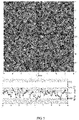
- With the increasing demands of the market and users, video walls (splicing screens) are constantly pursuing extremely narrow borders to achieve a better visual experience. However, due to the structure of sealing and encapsulating liquid crystals on the LCD screen, the black matrix on the edge and the technical limitations of the sealing area, black lines on the edges of the screen cannot be completely eliminated, and there will be an apparent black line, that is, a seam, after splicing screens, as shown in the B area in
FIG. 1 , which will seriously affect the visual effect of the user watching a displayed image. - Therefore, how to improve the user's visual effect and achieve a subjective visual feeling for the user as if there was no seam is a technical problem to be solved urgently in this field.
- The present disclosure provides an array substrate and a splicing display unit and a display screen, which can visually eliminate the seam, improve the user's visual effect on splicing screens, and achieve a subjective visual feeling for the user as if there was no seam.
- According to a first aspect of the embodiments of the present disclosure, there is provided a display screen, including a plurality of display modules and a plurality of optical structures, the plurality of display modules and the plurality of optical structures being closely arranged, wherein each of the optical structures is arranged corresponding to one of the display modules, and is arranged on a side of a light-emitting surface of the display module; adjacent two display modules are arranged close to each other, and optical structures on adjacent two display modules are arranged close to each other;
- each of the display modules includes a display area and a black edge area arranged around the display area, black edge areas of adjacent two display modules are spliced together to form a seam;
- each of the optical structures includes a first surface and a second surface disposed opposite to each other, and the second surface of the optical structure is attached to the display module;
- one end of the first surface of the optical structure close to the seam is a first arc surface, and the first arc surface is configured to refract light emitted from the display area of the display module, and then distribute the refracted light in a front-view area corresponding to the seam.
- Optionally, the first arc surface is a convex arc surface configuration.
- Optionally, a size of an orthographic projection of the first arc surface on the display module along a width direction of the seam is larger than or equal to a width of the seam, and smaller than or equal to the width of the
seam 30 plus 5 mm, and the width of the seam is 0.88mm-3.9mm; and/or, - the first arc surface includes a first end close to the display module and a second end away from the display module; a distance from a horizontal plane where the first end of the first arc surface is located to a horizontal plane where the second end of the first arc surface is located is smaller than or equal to one half of a thickness of the optical structure; and/or
- a radius of the first arc surface is larger than or equal to the width of the seam, and smaller than or equal to the width of the seam plus 5 mm, where the width of the seam is 0.88mm-3.9mm; and/or,
- the radius of the first arc surface is 2mm-5mm; and/or,
- a thickness of the optical structure is 3mm-10mm.
- Optionally, one end of the second surface of the optical structure close to the seam is a second arc surface, and light emitted from the display area of the display module is reflected by the second arc surface to supplement light in a non-front-view area corresponding to the seam.
- Optionally, the second arc surface is a concave arc surface configuration.
- Optionally, the second arc surface includes a third end close to the display module and a fourth end away from the display module; a distance from a horizontal plane where the fourth end is located to a horizontal plane where the third end is located is larger than or equal to one half of the width of the seam and smaller than or equal to the thickness of the optical structure minus 1 mm; and/or,
- a distance between one end of the first arc surface closest to the second surface and one end of the second arc surface closest to the first surface is larger than or equal to 0.3 mm, and smaller than or equal to 1 mm; and/or,
- a radius of the second arc surface is 2mm-8mm.
- According to a second aspect of the embodiments of the present disclosure, there is provided a splicing display unit, including a display module and an optical structure, the display module and the optical structure being stacked together, wherein the optical structure is arranged on one side of a light emitting surface of the display module;
- the display module includes a display area and a black edge area arranged around the display area;
- each optical structure includes a first surface and a second surface disposed opposite to each other, and the second surface of the optical structure is attached to the display module;
- one end of the first surface of the optical structure close to the black edge area of the display module is a first arc surface, and the first arc surface is configured to refract light emitted from the display area of the display module and distribute the refracted light in a front-view area corresponding to the black edge area.
- Optionally, the first arc surface is a convex arc surface configuration.
- Optionally, a size of an orthographic projection of the first arc surface on the display module along a width direction of the seam is larger than or equal to twice a width of the black edge area and smaller than or equal to twice the width of the black edge area plus 5mm, and the width of the black edge area is 0.44 mm-1.95 mm; and/or,
- the first arc surface includes a first end close to the display module and a second end away from the display module; a distance from a horizontal plane where the first end of the first arc surface is located to a horizontal plane where the second end of the first arc surface is located is smaller than or equal to one half of a thickness of the optical structure; and/or,
- a radius of the first arc surface is larger than or equal to twice the width of the black edge area, and smaller than or equal to twice the width of the black edge area plus 5mm, the width of the black edge area is 0.44mm-1.95mm; and/or,
- the radius of the first arc surface is 2mm-5mm; and/or;
- a thickness of the optical structure is 3mm-10mm.
- Optionally, one end of the second surface of the optical structure close to the black edge area of the display module is a second arc surface, and light emitted from the display area of the display module is reflected by the second arc surface to supplement light in a non-front-view area corresponding to the black edge area.
- Optionally, the second arc surface is a concave arc surface configuration.
- Optionally, the second arc surface includes a third end close to the display module and a fourth end away from the display module; a distance from a horizontal plane where the fourth end is located to a horizontal plane where the third end is located is larger than or equal to the width of the black edge area and smaller than or equal to the thickness of the
optical structure minus 1 mm, and the width of the black edge area is 0.44 mm -1.95mm; and/or, - a distance between one end of the first arc surface closest to the second surface and one end of the second arc surface closest to the first surface is larger than or equal to 0.3 mm, and smaller than or equal to 1 mm; and/or,
- a radius of the second arc surface is 2mm-8mm.
- In the display screen of the present disclosure, by providing the overall structure and providing the first arc surface in the optical structure, the light emitted from the display area of the display module can be refracted and distributed in the front-view area corresponding to the seam, which can visually eliminate the seam, improve the user's visual effect on splicing screens, and achieve a subjective visual feeling for the user as if there was no seam.
- In the splicing display unit of the present disclosure, by providing the overall structure and providing the first arc surface in the optical structure, the light emitted from the display area of the display module can be refracted and distributed in the front-view area corresponding to the black edge area, which can visually eliminate the black edge area, improve the user's visual effect on splicing screens, and achieve a subjective visual feeling for the user as if there was no black edge area.
-
-
FIG. 1 is a front view of a simulated luminance distribution diagram of a display screen in the prior art. -
FIG. 2 is a partial cross-sectional view of a display screen of Example 1 of the present application. -
FIG. 3 is a schematic diagram of a light path of light emitted by the display module of the display screen of Example 1 of the present application. -
FIG. 4 is a partial cross-sectional view of an optical structure of the display screen of Example 1 of the present application. -
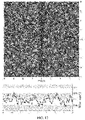
FIG. 5 is a front view of a simulated luminance distribution diagram of the display screen of Example 1 of the present application. -
FIG. 6 is a partial cross-sectional view of a display screen of Example 2 of the present application. -
FIG. 7 is a schematic diagram of an optical path of light emitted by a display module of a display screen of Example 2 of the present application. -
FIG. 8 is a partial cross-sectional view of an optical structure of the display screen of Example 2 of the present application. -
FIG. 9 is a front view of a simulated luminance distribution diagram of the display screen of Example 2 of the present application. -
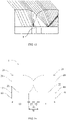
FIG. 10 is a 45-degree optical path diagram of the optical structure of the display screen of Example 1 of the present application. -
FIG. 11 is a schematic structural diagram of an optical structure of another implementation of the display screen of the present application. -
FIG. 12 is a front view of a simulated luminance distribution diagram of an optical structure of another implementation of the display screen of the present application. -
FIG. 13 is a 45-degree optical path diagram of an optical structure of another implementation of the display screen of the present application. -
FIG. 14 is a schematic structural diagram of an optical structure of another implementation of the display screen of the present application. -
FIG. 15 is a front view of a simulated luminance distribution diagram of an optical structure of still another implementation of the display screen of the present application. -
FIG. 16 is a 45-degree optical path diagram of an optical structure of still another implementation of the display screen of the present application. -
FIG. 17 is a 45-degree optical path diagram of an optical structure of the display screen of Example 2 of the present application. -
FIG. 18 is a schematic cross-sectional view of a splicing display unit of Example 3 of the present application. -
FIG. 19 is a schematic cross-sectional view of a splicing display unit of Example 4 of the present application. - Examples will be described in detail herein, with the illustrations thereof represented in the drawings. When the following descriptions involve the drawings, like numerals in different drawings refer to like or similar elements unless otherwise indicated. The embodiments described in the following examples do not represent all embodiments consistent with the present disclosure. Rather, they are merely examples of apparatuses and methods consistent with some aspects of the present disclosure as detailed in the appended claims.
- The terms used in the present disclosure are for the purpose of describing particular examples only, and are not intended to limit the present disclosure. Unless otherwise defined, technical or scientific terms used in this application shall have the ordinary meaning as understood by those of ordinary skill in the art to which this application belongs. Terms determined by "a" or "an" used in the specification and claims of this application also do not denote a quantitative limitation, but rather denote the presence of at least one. Terms like "comprise" or "include" mean that the elements or items appearing before "comprising" or "including" cover the elements or items listed after "comprising" or "including" and their equivalents, and do not exclude other elements or objects. "Connected to" or "connected with" and similar words are not limited to physical or mechanical connections, but can include electrical connections, whether direct or indirect. "A plurality of" includes two, equivalent to at least two. As used in this specification and the appended claims, the singular forms "a," "an," and "the" are intended to include the plural forms as well, unless the context clearly dictates otherwise. It will also be understood that the term "and/or" as used herein refers to and includes any and all possible combinations of one or more of the associated listed items.
- As shown in
FIG. 2 to FIG. 4 , this example provides adisplay screen 1. Thedisplay screen 1 includes a plurality ofdisplay modules 10 and a plurality ofoptical structures 20, the plurality of display modules and the plurality of optical structures being closely arranged. Each of theoptical structures 20 is arranged corresponding to one of thedisplay modules 10 and is arranged on a side of a light-emitting surface of thedisplay module 10. Adjacent twodisplay modules 10 are arranged close to each other, andoptical structures 20 on adjacent twodisplay modules 10 are arranged close to each other. - Each of the
display modules 10 includes adisplay area 11 and ablack edge area 12 arranged around thedisplay area 11, that is, thedisplay area 11 is located at the center of the display module, and theblack edge area 12 is arranged around thedisplay area 11, and located at the edge of the display module.Black edge areas 12 of adjacent twodisplay modules 10 are spliced together to form aseam 30. - Each of the
optical structures 20 includes afirst surface 21 and asecond surface 22 disposed opposite to each other, and thesecond surface 22 of theoptical structure 20 is attached to thedisplay module 10. - One end of the
first surface 21 of theoptical structure 20 close to theseam 30 is afirst arc surface 23, and thefirst arc surface 23 is configured to refract light emitted from thedisplay area 11 of thedisplay module 10 and then distribute the refracted light to a front-view area corresponding to theseam 30. As shown inFIG. 2 , the direction of the arrow in the figure is a propagation direction of the light emitted from thedisplay area 11 of thedisplay module 10. In order to more clearly show the propagation direction of the light emitted from thedisplay area 11 of thedisplay module 10, a cross section line is removed from the figure. - It should be noted that the front-view area corresponding to the
seam 30 refers to that an area where theseam 30 is observed when a user watches thedisplay module 10 from a front view angle (i.e., an angle perpendicular to the display module 10) in absence of an optical structure. - In this way, by providing the overall structure and providing the
first arc surface 23 in theoptical structure 20, the light emitted from thedisplay area 11 of thedisplay module 10 can be refracted and distributed in the front-view area corresponding to theseam 30, which can visually eliminate theseam 30, improve the user's visual effect on splicing screens, and achieve a subjective visual feeling for the user as if there was noseam 30. Specifically, the light is refracted by thefirst arc surface 23 of theoptical structure 20, so that thedisplay area 11 of thedisplay module 10 is "enlarged" to the imaging surface, so as to achieve the visual effect as if thephysical seam 30 of thedisplay screen 1 was eliminated. - Further, the
first arc surface 23 is a convex arc surface configuration. The convex arc surface configuration refers to that the arc surface is convex in a direction away from the center of the optical structure. And the end surface of thefirst arc surface 23 is located within the edge of theoptical structure 20. - That is to say, the
first arc surface 23 extends from a plane where thefirst surface 21 is located toward a direction close to thedisplay module 10 to form a convex arc surface configuration, thereby forming a structure similar to a convex lens, to implement refracting the light emitted from thedisplay area 11 of themodule 10 and distributing the refracted light in the front-view area corresponding to theseam 30. Further, by defining parameters of the structure of the convex lens, it is possible to make the optical path to be deviated from the incident light direction by a specific angle to achieve an effect of magnifying an image, thereby eliminating theseam 30 and improving the user experience. - In addition, compared with some
optical structures 20 in the prior art that are formed by overlapping several groups of prism structures, and the technical solutions in which several groups of prism structures are arranged to translate the image to the area of theseam 30, theoptical structure 20 of thedisplay screen 1 of this example has an image magnification effect, which can be suitable for N∗N splicing, and is a single structure, so as to avoid the change of the picture effect caused by offsets of multiple structures in assembling. - Specifically, as shown in
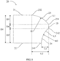
FIG. 3 , in order to more clearly show the arrangement of thefirst arc surface 23 in theoptical structure 20, the cross section line in the figure is removed. A size L2 of an orthographic projection of thefirst arc surface 23 on thedisplay module 10 along the width direction of theseam 30 is larger than or equal to the width W of theseam 30, and smaller than or equal to the width W of theseam 30 plus 5 mm. The width W of theseam 30 is 0.88mm-3.9mm. By making the size L2 of the orthographic projection of thefirst arc surface 23 on thedisplay module 10 along the width direction of theseam 30 to be larger than or equal to the width W of theseam 30, it is possible to block theseam 30, but if the size is too large, the effect of refraction will be reduced. - The
first arc surface 23 includes afirst end 231 close to thedisplay module 10 and asecond end 232 away from thedisplay module 10. A distance D3 from a horizontal plane where thefirst end 231 of thefirst arc surface 23 is located to a horizontal plane where thesecond end 232 of thefirst arc surface 23 is located is smaller than or equal to one half of a thickness D1 of theoptical structure 20. Within this range, the larger the value of the distance D3 from the horizontal plane where thefirst end 231 of thefirst arc surface 23 is located to the horizontal plane where thesecond end 232 of thefirst arc surface 23 is located, the better the refraction effect and the better the front view effect, but the larger thickness of the optical structure will increase the weight and material cost; which will be traded off during design. Preferably, the distance D3 from the horizontal plane where thefirst end 231 of thefirst arc surface 23 is located to the horizontal plane where thesecond end 232 of thefirst arc surface 23 is located is 2 mm-4 mm. - A radius R1 of the
first arc surface 23 is larger than or equal to the width W of theseam 30, and smaller than or equal to the width W of theseam 30 plus 5 mm. Preferably, the radius R1 of thefirst arc surface 23 is 2mm-5mm. - The arc length L1 of the
first arc surface 23 is defined collectively by the size L2 of the orthographic projection of thefirst arc surface 23 on thedisplay module 10 along the width direction of theseam 30, the distance D3 from the horizontal plane where thefirst end 231 of thefirst arc surface 23 is located to the horizontal plane where thesecond end 232 of thefirst arc surface 23 is located and the radius R1 of thefirst arc surface 23. The larger the arc length L1 of thefirst arc surface 23 is, the larger the length of the seam that can be covered is, which can be designed based on the length of the seam. - In this example, a thickness D1 of the
optical structure 20 is 3mm-10mm. The material of theoptical structure 20 is glass, or PMMA (polymethyl methacrylate), or PC (polycarbonate). Theoptical structure 20 is fixed on thedisplay module 10 through an opticaladhesive layer 40. - In this example, the
second surface 22 of theoptical structure 20 in this example is an integral flat plane. -
FIG. 5 is a front view of a simulated luminance distribution diagram of thedisplay screen 1 of this example. It can be seen fromFIG. 5 that a user will substantially not be able to observe theseam 30 at the front-view angle, so that theseam 30 can be visually eliminated, the user's visual effect on splicing screens can be improved, achieving a subjective visual feeling for the user as if there was noseam 30. - As shown in
FIG. 6-FIG. 9 , the overall structure of the display screen of this example is substantially the same as the structure in Example 1, except in that one end of thesecond surface 22 of theoptical structure 20 close to theseam 30 is asecond arc surface 24, and the light emitted from thedisplay area 11 of thedisplay module 10 is reflected by thesecond arc surface 24 to supplement the light in the non-front-view area corresponding to theseam 30. - It should be noted that the non-front-view area corresponding to the
seam 30 refers to an area where theseam 30 is observed when a user watches thedisplay module 10 from an angle other than the front view angle (that is, an angle that is not perpendicular to thedisplay module 10, that is, an oblique view angle or a large view angle) in absence of an optical structure. - In this way, by providing the
second arc surface 24, the light emitted from thedisplay area 11 of thedisplay module 10 can be reflected, and the light can be emitted through thefirst surface 21 of the light structure, so that the light can be supplemented for the non-front-view area corresponding to theseam 30. It can further visually eliminate theseam 30 for the non-front-view area corresponding to theseam 30, further improving the user's visual effect on a splicing screen, and achieving a subjective visual feeling for the user as if there was noseam 30. - Further, the
second arc surface 24 is a concave arc surface configuration. Wherein, the concave arc surface configuration refers to that the arc surface is concave in a direction close to the center of the optical structure. - Specifically, a size L4 of an orthographic projection of the
second arc surface 24 on thedisplay module 10 along the width direction of theseam 30 is larger than or equal to one half of the width W of theseam 30, and smaller than or equal to one half of the width W of theseam 30 plus 0.5mm, so as to cover the length of the seam from an oblique view angle. - The
second arc surface 24 includes athird end 241 close to thedisplay module 10 and afourth end 242 away from thedisplay module 10. - A distance D2 from the horizontal plane where the
fourth end 242 is located to the horizontal plane where thethird end 241 is located is larger than or equal to one half of the width W of theseam 30 plus 0.5mm, and the larger the value of D2 is, the better the oblique view angle effect will be, but the larger thickness of the optical structure will increase the weight and material cost; therefore, the oblique angle and the thickness of the model should be traded off in the design, and the distance D2 from the horizontal plane where thefourth end 242 is located to the horizontal plane where thethird end 241 is located is generally set to be larger than or equal to one half of the width of the seam and smaller than or equal to the thickness of the optical structure minus 1 mm. - A distance D4 between the end of the
first arc surface 23 closest to the second surface 22 (thefirst end 231 of the first arc surface 23) and the end of thesecond arc surface 24 closest to the first surface 21 (thefourth end 242 of the second arc surface 24) is larger than zero. Preferably, the distance D4 between thefirst end 231 of thefirst arc surface 23 and thefourth end 242 of thesecond arc surface 24 is larger than or equal to 0.3 mm, and smaller than or equal to 1 mm to avoid sharp corners during assembly and scratches during operation, and facilitates the processing of materials. It should be noted that when aside edge 25 connected between thefirst surface 21 and thesecond surface 22 is perpendicular to thedisplay module 10, a length of theside edge 25 is equal to the distance D4 between thefirst end 231 of thefirst arc surface 23 and thefourth end 242 of thesecond arc surface 24. - A radius R2 of the
second arc surface 24 is 2mm-8mm. The smaller the value of the radius R2 of thesecond arc surface 24 is, the better the effect of oblique view angle will be, but the worse the effect of front view angle will be; and vice versa. Therefore, the effect of oblique view angle and the effect of front view angle should be traded of during design. When the value of the radius R2 of thesecond arc surface 24 is 2mm-8mm, the effects will be optimal. The arc length L3 of thesecond arc surface 24 is determined jointly from the size L4 of the orthographic projection of thesecond arc surface 24 on thedisplay module 10 along the width direction of theseam 30, the distance D2 from the horizontal plane where thefourth end 242 is located to the horizontal plane where thethird end 241 is located and the radius R2 of thesecond arc surface 24. - The end of the
second surface 22 of theoptical structure 20 close to theseam 30 in this example is a concave arc surface configuration.FIG. 9 is a simulated luminance distribution diagram of thedisplay screen 1 of this example. It can be seen inFIG. 9 that, a user will substantially not be able to observe theseam 30 at the front view angle, which can visually eliminate theseam 30, improve the user's visual effect on splicing screens, and achieve a subjective visual feeling for the user as if there was noseam 30. - It should be noted that the end of the
second surface 22 close to theseam 30 can also be in other structural forms, but it has different effects on the optical path of the oblique view angle. - As in the
optical structure 20 in Example 1, when thesecond surface 22 is an integral flat plane, referring back toFIG. 5 , the user can hardly observe theseam 30 from a front angle. However, as shown inFIG. 10 , when watching thedisplay module 10 at an oblique angle of 45 degrees, the user can observe the structure of part of theseam 30, that is, the part O in the figure. That is, for theoptical structure 20 in Example 1, theseam 30 seen from a front view angle can be visually eliminated through thefirst arc surface 23, but theseam 30 seen by a user at an oblique view angle or a large view angle cannot be visually eliminated. - Similarly, in another example, as shown in
FIG. 11 , when the end of thesecond surface 22 of theoptical structure 20 close to theseam 30 is a flat surface that forms a certain angle with the plane where thedisplay module 10 is located, as shown inFIG. 12 , the user will substantially not be able to observe theseam 30 at a front angle. However, as shown inFIG. 13 , when the user watches thedisplay module 10 at an oblique angle of 45 degrees, the structure of part of theseam 30 can also be observed, that is, the part P in the figure. That is, when the end of thesecond surface 22 close to theseam 30 is set as a flat plane with a certain angle formed with the plane where thedisplay module 10 is located, only part of the light can be emitted out of theoptical structure 20, to alleviate the problem that the user can see theseam 30 in oblique or large view angles, which effect is less than desirable. - In yet another example, as shown in
FIG. 14 , when the end of thesecond surface 22 of theoptical structure 20 close to theseam 30 is a convex arc structure, as shown inFIG. 15 , the user will substantially not be able to observe theseam 30 at a front angle. However, as shown inFIG. 16 , when the user watches thedisplay module 10 at an oblique angle of 45 degrees, the user can still observe a part of the structure of theseam 30, that is, the part Q in the figure. That is to say, when the end of thesecond surface 22 close to theseam 30 is provided as a convex arc structure, only a very small part of the light can be emitted out of theoptical structure 20, to alleviate the problem that the user can see theseam 30 in oblique or large view angles, which effect is undesirable. - Only with the configuration of Example 2 in which the end of the
second surface 22 of theoptical structure 20 close to theseam 30 is a concave arc structure, not only the user will substantially not be able to observe theseam 30 at a front angle (referring back toFIG. 9 ); but also, when the user watches thedisplay module 10 at an oblique angle of 45 degrees (as shown inFIG. 17 ), theseam 30 cannot be observed at all. That is, when the end of thesecond surface 22 close to theseam 30 is configured as a concave arc structure, all light can exit theoptical structure 20 to alleviate the problem that the user can see theseam 30 in a large view angle, which effect is desirable. - Through the above description, the optimal
optical structure 2 can be obtained in which one end of thefirst surface 21 close to theseam 30 is a convex arc structure and one end of thesecond surface 22 close to theseam 30 is a concave arc structure. This can eliminate the seam from both the front view angle and the large view angle. - As shown in
FIG. 18 , in this example, there is provided asplicing display unit 2. A plurality ofsplicing display units 2 are closely arranged to form the display screen in Example 1. That is, thesplicing display unit 2 in this example is the smallest splicing unit of the display screen in Example 1. - The
splicing display unit 2 includes adisplay module 10 and anoptical structure 20, the display module and the optical structure being stacked together, and theoptical structure 20 is arranged on one side of the light emitting surface of thedisplay module 10. The configuration of theoptical structure 20 of this example can be made toFIG. 4 . - The
display module 10 includes adisplay area 11 and ablack edge area 12 arranged around thedisplay area 11, that is, thedisplay area 11 is located at the center of thedisplay module 10, and theblack edge area 12 is arranged around thedisplay area 11, so as to be located at the edge of thedisplay module 11. When a plurality ofsplicing display units 2 are closely arranged, theblack edge areas 12 of adjacent twodisplay modules 10 are spliced together to form theseam 30 of the display screen in Example 1. - Each of the
optical structures 20 includes afirst surface 21 and asecond surface 22 disposed opposite to each other, and thesecond surface 22 of theoptical structure 20 is attached to thedisplay module 10. - One end of the
first surface 21 of theoptical structure 20 close to theblack edge area 12 of thedisplay module 10 is afirst arc surface 23, and thefirst arc surface 23 is configured to refract the light emitted from thedisplay area 11 of thedisplay module 10, and then distribute the refracted light in the front-view area corresponding to theblack edge area 12. - It should be noted that the front-view area corresponding to the
black edge area 12 refers to that an area where theblack edge area 12 is observed when a user watches thedisplay module 10 from a front view angle (i.e., an angle perpendicular to the display module 10) in absence of an optical structure. - In this way, by providing the overall structure and providing the
first arc surface 23 in theoptical structure 20, the light emitted from thedisplay area 11 of thedisplay module 10 can be refracted and distributed in the front-view area corresponding to theblack edge area 12, which can visually eliminate theblack edge area 12, improve the user's visual effect on splicing screens, and achieve a subjective visual feeling for the user as if there was noblack edge area 12. Specifically, the light is refracted by thefirst arc surface 23 of theoptical structure 20, so that thedisplay area 11 of thedisplay module 10 is "enlarged" to the imaging surface, so as to achieve the visual effect as if the physicalblack edge area 12 of thedisplay screen 1 was eliminated. - Further, a distance from the
first arc surface 23 to the plane where thedisplay module 10 is located gradually decreases from a direction away from thedisplay module 10 to a direction close to thedisplay module 10, and thefirst arc surface 23 is a convex arc surface configuration. The convex arc surface configuration refers to that the arc surface is convex in a direction away from the center of the optical structure. - That is to say, the
first arc surface 23 extends from a plane where thefirst surface 21 is located toward a direction close to thedisplay module 10 to form a convex arc surface configuration, thereby forming a structure similar to a convex lens, to implement refracting the light emitted from thedisplay area 11 of themodule 10 and distributing the refracted light in the front-view area corresponding to theblack edge area 12. Further, by defining parameters of the structure of the convex lens, it is possible to make the optical path to be deviated from the incident light direction by a specific angle to achieve an effect of magnifying an image, thereby eliminating theblack edge area 12 and improving the user experience. - In addition, compared with some
optical structures 20 in the prior art that are formed by overlapping several groups of prism structures, and the technical solutions in which several groups of prism structures are arranged to translate the image to the area of theblack edge area 12, theoptical structure 20 of thedisplay screen 1 of this example has an image magnification effect, which can be suitable for N∗N splicing, and is a single structure, so as to avoid the change of the picture effect caused by offsets of multiple structures in assembling. - Specifically, as shown in
FIG. 3 , in order to more clearly show the arrangement of thefirst arc surface 23 in theoptical structure 20, the cross section line in the figure is removed. A size L2 of an orthographic projection of thefirst arc surface 23 on thedisplay module 10 along the width direction of theblack edge area 12 is larger than or equal to twice the width w of theblack edge area 12, and smaller than or equal to twice the width w of theblack edge area 12 plus 5 mm. The width w of theblack edge area 12 is 0.44 mm-1.95mm. By making the size L2 of the orthographic projection of thefirst arc surface 23 on thedisplay module 10 along the width direction of theblack edge area 12 to be larger than or equal to twice the width w of theblack edge area 12, it is possible to block theblack edge area 12, but if the size is too large, the effect of refraction will be reduced. - The
first arc surface 23 includes afirst end 231 close to thedisplay module 10 and asecond end 232 away from thedisplay module 10. A distance D3 from a horizontal plane where thefirst end 231 of thefirst arc surface 23 is located to a horizontal plane where thesecond end 232 of thefirst arc surface 23 is located is smaller than or equal to one half of a thickness D1 of theoptical structure 20. Within this range, the larger the value of the distance D3 from the horizontal plane where thefirst end 231 of thefirst arc surface 23 is located to the horizontal plane where thesecond end 232 of thefirst arc surface 23 is located, the better the refraction effect and the better the front view effect, but the larger thickness of the optical structure will increase the weight and material cost; which will be traded off during design. Preferably, the distance D3 from the horizontal plane where thefirst end 231 of thefirst arc surface 23 is located to the horizontal plane where thesecond end 232 of thefirst arc surface 23 is located is 2 mm-4 mm. - A radius R1 of the
first arc surface 23 is larger than or equal to twice the width w of theblack edge area 12, and smaller than or equal to twice the width w of theblack edge area 12 plus 5 mm. Preferably, the radius R1 of thefirst arc surface 23 is 2mm-5mm. - The arc length L1 of the
first arc surface 23 is defined collectively by the size L2 of the orthographic projection of thefirst arc surface 23 on thedisplay module 10 along the width direction of theblack edge area 12, the distance D3 from the horizontal plane where thefirst end 231 of thefirst arc surface 23 is located to the horizontal plane where thesecond end 232 of thefirst arc surface 23 is located and the radius R1 of thefirst arc surface 23. The larger the arc length L1 of thefirst arc surface 23 is, the larger the length of the seam that can be covered is, which can be designed based on the length of the seam. - In this example, a thickness D1 of the
optical structure 20 is 3mm-10mm. The material of theoptical structure 20 is glass, or PMMA (polymethyl methacrylate), or PC (polycarbonate). Theoptical structure 20 is fixed on thedisplay module 10 through an opticaladhesive layer 40. - In this example, the
second surface 22 of theoptical structure 20 in this example is an integral flat plane. - The
splicing display unit 2 of the present example can visually eliminate theblack edge area 12. The user's visual effect on splicing screens can be improved, achieving a subjective visual feeling for the user as if there was noblack edge area 12. - As shown in
FIG. 19 , the overall structure of the splicing display unit of this example is substantially the same as the structure in Example 3, except in that one end of thesecond surface 22 of theoptical structure 20 close to theblack edge area 12 is asecond arc surface 24, and the light emitted from thedisplay area 11 of thedisplay module 10 is reflected by thesecond arc surface 24 to supplement the light in the non-front-view area corresponding to theblack edge area 12. The configuration of theoptical structure 20 of this example can refer toFIG. 8 . - It should be noted that the non-front-view area corresponding to the
black edge area 12 refers to an area where theblack edge area 12 is observed when a user watches thedisplay module 10 from an angle other than the front view angle (that is, an angle that is not perpendicular to thedisplay module 10, that is, an oblique view angle or a large view angle) in absence of an optical structure. - In this way, by providing the
second arc surface 24, the light emitted from thedisplay area 11 of thedisplay module 10 can be reflected, and the light can be emitted through thefirst surface 21 of the light structure, so that the light can be supplemented for the non-front-view area corresponding to theblack edge area 12. It can further visually eliminate theblack edge area 12 for the non-front-view area corresponding to theblack edge area 12, further improving the user's visual effect on a splicing screen, and achieving a subjective visual feeling for the user as if there was noblack edge area 12. - Further, the
second arc surface 24 is a concave arc surface configuration. Wherein, the concave arc surface configuration refers to that the arc surface is concave in a direction close to the center of the optical structure. - Specifically, a size L4 of an orthographic projection of the
second arc surface 24 on thedisplay module 10 along the width direction of theblack edge area 12 is larger than or equal to the width w of theblack edge area 12, and smaller than or equal to the width w of theblack edge area 12 plus 0.5mm, so as to cover the length of the seam from an oblique view angle. - The
second arc surface 24 includes athird end 241 close to thedisplay module 10 and afourth end 242 away from thedisplay module 10. - A distance D2 from the horizontal plane where the
fourth end 242 is located to the horizontal plane where thethird end 241 is located is larger than or equal to the width w of theblack edge area 12 plus 0.5mm, and the larger the value of D2 is, the better the oblique view angle effect will be, but the larger thickness of the optical structure will increase the weight and material cost; therefore, the oblique angle and the thickness of the model should be traded off in the design, and the distance D2 from the horizontal plane where thefourth end 242 is located to the horizontal plane where thethird end 241 is located is generally set to be larger than or equal to the width w of theblack edge area 12 and smaller than or equal to the thickness of the optical structure minus 1 mm. - A distance D4 between the end of the
first arc surface 23 closest to the second surface 22 (thefirst end 231 of the first arc surface 23) and the end of thesecond arc surface 24 closest to the first surface 21 (thefourth end 242 of the second arc surface 24) is larger than zero. Preferably, the distance D4 between thefirst end 231 of thefirst arc surface 23 and thefourth end 242 of thesecond arc surface 24 is larger than or equal to 0.3 mm, and smaller than or equal to 1 mm to avoid sharp corners during assembly and scratches during operation, and facilitates the processing of materials. It should be noted that when aside edge 25 connected between thefirst surface 21 and thesecond surface 22 is perpendicular to thedisplay module 10, a length of theside edge 25 is equal to the distance D4 between thefirst end 231 of thefirst arc surface 23 and thefourth end 242 of thesecond arc surface 24. - A radius R2 of the
second arc surface 24 is 2mm-8mm. The smaller the value of the radius R2 of thesecond arc surface 24 is, the better the effect of oblique view angle will be, but the worse the effect of front view angle will be; and vice versa. Therefore, the effect of oblique view angle and the effect of front view angle should be traded of during design. When the value of the radius R2 of thesecond arc surface 24 is 2mm-8mm, the effects will be optimal. The arc length L3 of thesecond arc surface 24 is determined jointly from the size L4 of the orthographic projection of thesecond arc surface 24 on thedisplay module 10 along the width direction of theblack edge area 12, the distance D2 from the horizontal plane where thefourth end 242 is located to the horizontal plane where thethird end 241 is located and the radius R2 of thesecond arc surface 24. - With the configuration of Example 2 in which the end of the
second surface 22 of theoptical structure 20 close to theblack edge area 12 is a concave arc structure, not only the user will substantially not be able to observe theblack edge area 12 at a front angle; but also, when the user watches thedisplay module 10 at an oblique angle of 45 degrees, theblack edge area 12 cannot be observed at all. That is, when the end of thesecond surface 22 close to theblack edge area 12 is configured as a concave arc structure, all light can exit theoptical structure 20 to alleviate the problem that the user can see theblack edge area 12 in a large view angle, which effect is desirable. - The
optical structure 2 can be obtained in which one end of thefirst surface 21 close to theblack edge area 12 is a convex arc structure and one end of thesecond surface 22 close to theblack edge area 12 is a concave arc structure. This can eliminate the seam from both the front view angle and the large view angle. - The above is only the preferred example of the application, and is not intended to limit the application. Within the spirit and principle of the application, any modification, equivalent replacement, improvement etc. made should fall within the scope of protection of this application.
Claims (12)
- A display screen, comprising a plurality of display modules and a plurality of optical structures, the plurality of display modules and the plurality of optical structures being closely arranged, wherein the optical structure is arranged corresponding to one of the display modules, and is arranged on a side of a light-emitting surface of the display module; adjacent two display modules are arranged close to each other, and optical structures on adjacent two display modules are arranged close to each other;the display module comprises a display area and a black edge area arranged around the display area, black edge areas of adjacent two display modules are spliced together to form a seam;the optical structure comprises a first surface and a second surface disposed opposite to each other, and the second surface of the optical structure is attached to the display module;one end of the first surface of the optical structure close to the seam is a first arc surface, and the first arc surface is configured to refract light emitted from the display area of the display module, and then distribute the refracted light in a front-view area corresponding to the seam.
- The display screen of claim 1, wherein the first arc surface is a convex arc surface configuration.
- The display screen of claim 1, wherein a size of an orthographic projection of the first arc surface on the display module along a width direction of the seam is larger than or equal to a width of the seam, and smaller than or equal to the width of the seam plus 5 mm, and the width of the seam is 0.88mm-3.9mm; and/or,the first arc surface comprises a first end close to the display module and a second end away from the display module; a distance from a horizontal plane where the first end of the first arc surface is located to a horizontal plane where the second end of the first arc surface is located is smaller than or equal to one half of a thickness of the optical structure; and/or a radius of the first arc surface is larger than or equal to the width of the seam, and smaller than or equal to the width of the seam plus 5 mm, where the width of the seam is 0.88mm-3.9mm; and/or,the radius of the first arc surface is 2mm-5mm; and/or,a thickness of the optical structure is 3mm-10mm.
- The display screen of any one of claims 1-3, wherein one end of the second surface of the optical structure close to the seam is a second arc surface, and light emitted from the display area of the display module is reflected by the second arc surface to supplement light in a non-front-view area corresponding to the seam.
- The display screen of claim 4, wherein the second arc surface is a concave arc surface configuration.
- The display screen of claim 4, wherein the second arc surface comprises a third end close to the display module and a fourth end away from the display module; a distance from a horizontal plane where the fourth end is located to a horizontal plane where the third end is located is larger than or equal to one half of the width of the seam and smaller than or equal to the thickness of the optical structure minus 1 mm; and/or,a distance between one end of the first arc surface closest to the second surface and one end of the second arc surface closest to the first surface is larger than or equal to 0.3 mm, and smaller than or equal to 1 mm; and/or,a radius of the second arc surface is 2mm-8mm.
- A splicing display unit, comprising a display module and an optical structure, the display module and the optical structure being stacked together, wherein the optical structure is arranged on one side of a light emitting surface of the display module;the display module comprises a display area and a black edge area arranged around the display area;the optical structure comprises a first surface and a second surface disposed opposite to each other, and the second surface of the optical structure is attached to the display module;one end of the first surface of the optical structure close to the black edge area of the display module is a first arc surface, and the first arc surface is configured to refract light emitted from the display area of the display module and distribute the refracted light in a front-view area corresponding to the black edge area.
- The splicing display unit of claim 7, wherein the first arc surface is a convex arc surface configuration.
- The splicing display unit of claim 7, wherein a size of an orthographic projection of the first arc surface on the display module along a width direction of the black edge area is larger than or equal to twice a width of the black edge area and smaller than or equal to twice the width of the black edge area plus 5mm, and the width of the black edge area is 0.44 mm-1.95 mm; and/or,the first arc surface comprises a first end close to the display module and a second end away from the display module; a distance from a horizontal plane where the first end of the first arc surface is located to a horizontal plane where the second end of the first arc surface is located is smaller than or equal to one half of a thickness of the optical structure; and/or,a radius of the first arc surface is larger than or equal to twice the width of the black edge area, and smaller than or equal to twice the width of the black edge area plus 5mm, the width of the black edge area is 0.44mm-1.95mm; and/or,the radius of the first arc surface is 2mm-5mm; and/or;a thickness of the optical structure is 3mm-10mm.
- The splicing display unit of any one of claims 7-9, wherein one end of the second surface of the optical structure close to the black edge area of the display module is a second arc surface, and light emitted from the display area of the display module is reflected by the second arc surface to supplement light in a non-front-view area corresponding to the black edge area.
- The splicing display unit of claim 10, wherein the second arc surface is a concave arc surface configuration.
- The splicing display unit of claim 10, wherein the second arc surface comprises a third end close to the display module and a fourth end away from the display module; a distance from a horizontal plane where the fourth end is located to a horizontal plane where the third end is located is larger than or equal to the width of the black edge area and smaller than or equal to the thickness of the optical structure minus 1 mm, and the width of the black edge area is 0.44 mm -1.95mm; and/or,a distance between one end of the first arc surface closest to the second surface and one end of the second arc surface closest to the first surface is larger than or equal to 0.3 mm, and smaller than or equal to 1 mm; and/or,a radius of the second arc surface is 2mm-8mm.
Applications Claiming Priority (1)
| Application Number | Priority Date | Filing Date | Title |
|---|---|---|---|
| PCT/CN2021/083428 WO2022198679A1 (en) | 2021-03-26 | 2021-03-26 | Splicing display unit and display screen |
Publications (3)
| Publication Number | Publication Date |
|---|---|
| EP4120227A1 true EP4120227A1 (en) | 2023-01-18 |
| EP4120227A4 EP4120227A4 (en) | 2023-04-26 |
| EP4120227B1 EP4120227B1 (en) | 2024-12-25 |
Family
ID=83395082
Family Applications (1)
| Application Number | Title | Priority Date | Filing Date |
|---|---|---|---|
| EP21932298.9A Active EP4120227B1 (en) | 2021-03-26 | 2021-03-26 | Splicing display unit and display screen |
Country Status (6)
| Country | Link |
|---|---|
| US (1) | US12326576B2 (en) |
| EP (1) | EP4120227B1 (en) |
| JP (1) | JP7723014B2 (en) |
| KR (1) | KR102865981B1 (en) |
| CN (1) | CN115413355B (en) |
| WO (1) | WO2022198679A1 (en) |
Families Citing this family (1)
| Publication number | Priority date | Publication date | Assignee | Title |
|---|---|---|---|---|
| CN114973987A (en) * | 2022-06-16 | 2022-08-30 | Tcl华星光电技术有限公司 | Video Wall |
Family Cites Families (21)
| Publication number | Priority date | Publication date | Assignee | Title |
|---|---|---|---|---|
| GB0028890D0 (en) | 2000-11-27 | 2001-01-10 | Isis Innovation | Visual display screen arrangement |
| GB0223883D0 (en) | 2002-10-15 | 2002-11-20 | Seamless Display Ltd | Visual display screen arrangement |
| CN102067196B (en) | 2008-06-25 | 2014-04-23 | 夏普株式会社 | Display device |
| CN102067197A (en) | 2008-06-26 | 2011-05-18 | 夏普株式会社 | Display device and electronic device |
| CN101770732B (en) | 2009-01-07 | 2011-07-06 | 曹嘉灿 | Seamless tiled display device |
| US8804317B2 (en) | 2009-07-01 | 2014-08-12 | Sharp Kabushiki Kaisha | Display device |
| US20140104712A1 (en) * | 2012-03-26 | 2014-04-17 | Dai Nippon Printing Co., Ltd | Array-type display apparatus |
| JP5382168B1 (en) | 2012-06-20 | 2014-01-08 | 大日本印刷株式会社 | Array type display device |
| CN103903518A (en) | 2012-12-25 | 2014-07-02 | 鸿富锦精密工业(深圳)有限公司 | Television wall and black frame eliminating lens thereof |
| KR20150031623A (en) | 2013-09-16 | 2015-03-25 | 삼성전자주식회사 | Tiled display system |
| CN203689856U (en) * | 2014-01-26 | 2014-07-02 | 京东方科技集团股份有限公司 | Display panel and display device |
| CN104123885A (en) | 2014-07-15 | 2014-10-29 | 青岛海信电器股份有限公司 | Seamless splicing display device |
| CN204375351U (en) | 2015-01-20 | 2015-06-03 | 张慧芳 | A kind of seamless splicing display device |
| TW201719201A (en) * | 2015-11-27 | 2017-06-01 | 鴻海精密工業股份有限公司 | Optical film and narrow bezel display device |
| CN105448196B (en) | 2015-12-21 | 2018-08-17 | 曹嘉灿 | A kind of blanking frame display device and display |
| CN205845413U (en) | 2016-07-27 | 2016-12-28 | 京东方科技集团股份有限公司 | A kind of tiled display panel and display device |
| CN207165134U (en) | 2017-09-05 | 2018-03-30 | 南京中冠智能科技有限公司 | A kind of seamless spliced screen |
| CN207302510U (en) * | 2017-10-20 | 2018-05-01 | 叶挺 | Seamless liquid crystal-spliced display device |
| CN108564894A (en) | 2018-04-16 | 2018-09-21 | 深圳市奔硕星光电科技有限公司 | A kind of liquid crystal-spliced seamless display device |
| CN110456552A (en) * | 2019-08-13 | 2019-11-15 | 杨冠男 | A large-scale seamless splicing display system |
| CN210924147U (en) | 2019-12-31 | 2020-07-03 | 湖北金小麦信息技术有限公司 | Micro-margin LCD display screen for splicing |
-
2021
- 2021-03-26 CN CN202180000614.8A patent/CN115413355B/en active Active
- 2021-03-26 US US17/767,740 patent/US12326576B2/en active Active
- 2021-03-26 WO PCT/CN2021/083428 patent/WO2022198679A1/en not_active Ceased
- 2021-03-26 KR KR1020237001276A patent/KR102865981B1/en active Active
- 2021-03-26 EP EP21932298.9A patent/EP4120227B1/en active Active
- 2021-03-26 JP JP2022573355A patent/JP7723014B2/en active Active
Also Published As
| Publication number | Publication date |
|---|---|
| US12326576B2 (en) | 2025-06-10 |
| KR20230160773A (en) | 2023-11-24 |
| JP2024510859A (en) | 2024-03-12 |
| EP4120227B1 (en) | 2024-12-25 |
| KR102865981B1 (en) | 2025-09-29 |
| CN115413355A (en) | 2022-11-29 |
| US20240094442A1 (en) | 2024-03-21 |
| EP4120227A4 (en) | 2023-04-26 |
| WO2022198679A1 (en) | 2022-09-29 |
| JP7723014B2 (en) | 2025-08-13 |
| CN115413355B (en) | 2025-03-18 |
Similar Documents
| Publication | Publication Date | Title |
|---|---|---|
| US8531623B2 (en) | Display device | |
| RU2507550C2 (en) | Optical assembly and autostereoscopic display device based thereon | |
| CN102414730B (en) | Display device | |
| US8482691B2 (en) | Display apparatus having a minimized non-display region | |
| US8045272B2 (en) | Display apparatus | |
| US20110164318A1 (en) | Display device and lenticular sheet of the display device | |
| CN102349293B (en) | Display device | |
| US10649131B2 (en) | Display device and head-mounted display | |
| US9081225B2 (en) | Liquid crystal display device | |
| CN110456552A (en) | A large-scale seamless splicing display system | |
| WO2012073929A1 (en) | Liquid crystal display device and multi-display system | |
| US20210294018A1 (en) | Display device and head-mounted display | |
| CN110178171B (en) | multiple monitors | |
| CN105652511A (en) | Display device | |
| CN105700269A (en) | Display device | |
| US12326576B2 (en) | Splicing display unit and display screen | |
| JP2009163245A (en) | Optical sheet and display device having the same | |
| CN116469319A (en) | A seamless splicing display system and light displacement device | |
| US20100134403A1 (en) | Light guide panel comprising symmetric fornt prism and asymmetric front prism for back light unit of lcd | |
| CN211478810U (en) | Large-size seamless splicing display system | |
| JP6289782B1 (en) | Multi display | |
| CN222482527U (en) | 3D naked-eye optical film and display device | |
| JP7445214B2 (en) | Optical structures, polarizing plates with optical structures, and display devices | |
| JPH09179113A (en) | Liquid crystal display | |
| JP2013200971A (en) | Light guide plate, backlight unit, and display device |
Legal Events
| Date | Code | Title | Description |
|---|---|---|---|
| STAA | Information on the status of an ep patent application or granted ep patent |
Free format text: STATUS: THE INTERNATIONAL PUBLICATION HAS BEEN MADE |
|
| PUAI | Public reference made under article 153(3) epc to a published international application that has entered the european phase |
Free format text: ORIGINAL CODE: 0009012 |
|
| STAA | Information on the status of an ep patent application or granted ep patent |
Free format text: STATUS: REQUEST FOR EXAMINATION WAS MADE |
|
| 17P | Request for examination filed |
Effective date: 20221012 |
|
| AK | Designated contracting states |
Kind code of ref document: A1 Designated state(s): AL AT BE BG CH CY CZ DE DK EE ES FI FR GB GR HR HU IE IS IT LI LT LU LV MC MK MT NL NO PL PT RO RS SE SI SK SM TR |
|
| REG | Reference to a national code |
Ref country code: DE Ref legal event code: R079 Free format text: PREVIOUS MAIN CLASS: G09F0009000000 Ipc: G02F0001133300 Ref country code: DE Ref legal event code: R079 Ref document number: 602021024057 Country of ref document: DE Free format text: PREVIOUS MAIN CLASS: G09F0009000000 Ipc: G02F0001133300 |
|
| A4 | Supplementary search report drawn up and despatched |
Effective date: 20230324 |
|
| RIC1 | Information provided on ipc code assigned before grant |
Ipc: G02F 1/1335 20060101ALI20230321BHEP Ipc: G09F 9/302 20060101ALI20230321BHEP Ipc: G02F 1/1333 20060101AFI20230321BHEP |
|
| DAV | Request for validation of the european patent (deleted) | ||
| DAX | Request for extension of the european patent (deleted) | ||
| GRAP | Despatch of communication of intention to grant a patent |
Free format text: ORIGINAL CODE: EPIDOSNIGR1 |
|
| STAA | Information on the status of an ep patent application or granted ep patent |
Free format text: STATUS: GRANT OF PATENT IS INTENDED |
|
| INTG | Intention to grant announced |
Effective date: 20240828 |
|
| GRAS | Grant fee paid |
Free format text: ORIGINAL CODE: EPIDOSNIGR3 |
|
| GRAA | (expected) grant |
Free format text: ORIGINAL CODE: 0009210 |
|
| STAA | Information on the status of an ep patent application or granted ep patent |
Free format text: STATUS: THE PATENT HAS BEEN GRANTED |
|
| AK | Designated contracting states |
Kind code of ref document: B1 Designated state(s): AL AT BE BG CH CY CZ DE DK EE ES FI FR GB GR HR HU IE IS IT LI LT LU LV MC MK MT NL NO PL PT RO RS SE SI SK SM TR |
|
| REG | Reference to a national code |
Ref country code: GB Ref legal event code: FG4D |
|
| REG | Reference to a national code |
Ref country code: CH Ref legal event code: EP |
|
| REG | Reference to a national code |
Ref country code: DE Ref legal event code: R096 Ref document number: 602021024057 Country of ref document: DE |
|
| REG | Reference to a national code |
Ref country code: IE Ref legal event code: FG4D |
|
| REG | Reference to a national code |
Ref country code: LT Ref legal event code: MG9D |
|
| PG25 | Lapsed in a contracting state [announced via postgrant information from national office to epo] |
Ref country code: HR Free format text: LAPSE BECAUSE OF FAILURE TO SUBMIT A TRANSLATION OF THE DESCRIPTION OR TO PAY THE FEE WITHIN THE PRESCRIBED TIME-LIMIT Effective date: 20241225 |
|
| PG25 | Lapsed in a contracting state [announced via postgrant information from national office to epo] |
Ref country code: FI Free format text: LAPSE BECAUSE OF FAILURE TO SUBMIT A TRANSLATION OF THE DESCRIPTION OR TO PAY THE FEE WITHIN THE PRESCRIBED TIME-LIMIT Effective date: 20241225 |
|
| PG25 | Lapsed in a contracting state [announced via postgrant information from national office to epo] |
Ref country code: BG Free format text: LAPSE BECAUSE OF FAILURE TO SUBMIT A TRANSLATION OF THE DESCRIPTION OR TO PAY THE FEE WITHIN THE PRESCRIBED TIME-LIMIT Effective date: 20241225 |
|
| PG25 | Lapsed in a contracting state [announced via postgrant information from national office to epo] |
Ref country code: NO Free format text: LAPSE BECAUSE OF FAILURE TO SUBMIT A TRANSLATION OF THE DESCRIPTION OR TO PAY THE FEE WITHIN THE PRESCRIBED TIME-LIMIT Effective date: 20250325 |
|
| PG25 | Lapsed in a contracting state [announced via postgrant information from national office to epo] |
Ref country code: GR Free format text: LAPSE BECAUSE OF FAILURE TO SUBMIT A TRANSLATION OF THE DESCRIPTION OR TO PAY THE FEE WITHIN THE PRESCRIBED TIME-LIMIT Effective date: 20250326 Ref country code: LV Free format text: LAPSE BECAUSE OF FAILURE TO SUBMIT A TRANSLATION OF THE DESCRIPTION OR TO PAY THE FEE WITHIN THE PRESCRIBED TIME-LIMIT Effective date: 20241225 |
|
| PGFP | Annual fee paid to national office [announced via postgrant information from national office to epo] |
Ref country code: AT Payment date: 20250417 Year of fee payment: 5 |
|
| PG25 | Lapsed in a contracting state [announced via postgrant information from national office to epo] |
Ref country code: RS Free format text: LAPSE BECAUSE OF FAILURE TO SUBMIT A TRANSLATION OF THE DESCRIPTION OR TO PAY THE FEE WITHIN THE PRESCRIBED TIME-LIMIT Effective date: 20250325 |
|
| REG | Reference to a national code |
Ref country code: NL Ref legal event code: MP Effective date: 20241225 |
|
| PG25 | Lapsed in a contracting state [announced via postgrant information from national office to epo] |
Ref country code: NL Free format text: LAPSE BECAUSE OF FAILURE TO SUBMIT A TRANSLATION OF THE DESCRIPTION OR TO PAY THE FEE WITHIN THE PRESCRIBED TIME-LIMIT Effective date: 20241225 |
|
| REG | Reference to a national code |
Ref country code: AT Ref legal event code: MK05 Ref document number: 1754671 Country of ref document: AT Kind code of ref document: T Effective date: 20241225 |
|
| PG25 | Lapsed in a contracting state [announced via postgrant information from national office to epo] |
Ref country code: SM Free format text: LAPSE BECAUSE OF FAILURE TO SUBMIT A TRANSLATION OF THE DESCRIPTION OR TO PAY THE FEE WITHIN THE PRESCRIBED TIME-LIMIT Effective date: 20241225 |
|
| PG25 | Lapsed in a contracting state [announced via postgrant information from national office to epo] |
Ref country code: PL Free format text: LAPSE BECAUSE OF FAILURE TO SUBMIT A TRANSLATION OF THE DESCRIPTION OR TO PAY THE FEE WITHIN THE PRESCRIBED TIME-LIMIT Effective date: 20241225 |
|
| PG25 | Lapsed in a contracting state [announced via postgrant information from national office to epo] |
Ref country code: ES Free format text: LAPSE BECAUSE OF FAILURE TO SUBMIT A TRANSLATION OF THE DESCRIPTION OR TO PAY THE FEE WITHIN THE PRESCRIBED TIME-LIMIT Effective date: 20241225 |
|
| PG25 | Lapsed in a contracting state [announced via postgrant information from national office to epo] |
Ref country code: IS Free format text: LAPSE BECAUSE OF FAILURE TO SUBMIT A TRANSLATION OF THE DESCRIPTION OR TO PAY THE FEE WITHIN THE PRESCRIBED TIME-LIMIT Effective date: 20250425 |
|
| PG25 | Lapsed in a contracting state [announced via postgrant information from national office to epo] |
Ref country code: PT Free format text: LAPSE BECAUSE OF FAILURE TO SUBMIT A TRANSLATION OF THE DESCRIPTION OR TO PAY THE FEE WITHIN THE PRESCRIBED TIME-LIMIT Effective date: 20250428 |
|
| PG25 | Lapsed in a contracting state [announced via postgrant information from national office to epo] |
Ref country code: EE Free format text: LAPSE BECAUSE OF FAILURE TO SUBMIT A TRANSLATION OF THE DESCRIPTION OR TO PAY THE FEE WITHIN THE PRESCRIBED TIME-LIMIT Effective date: 20241225 |
|
| PG25 | Lapsed in a contracting state [announced via postgrant information from national office to epo] |
Ref country code: RO Free format text: LAPSE BECAUSE OF FAILURE TO SUBMIT A TRANSLATION OF THE DESCRIPTION OR TO PAY THE FEE WITHIN THE PRESCRIBED TIME-LIMIT Effective date: 20241225 Ref country code: AT Free format text: LAPSE BECAUSE OF FAILURE TO SUBMIT A TRANSLATION OF THE DESCRIPTION OR TO PAY THE FEE WITHIN THE PRESCRIBED TIME-LIMIT Effective date: 20241225 |
|
| PG25 | Lapsed in a contracting state [announced via postgrant information from national office to epo] |
Ref country code: SK Free format text: LAPSE BECAUSE OF FAILURE TO SUBMIT A TRANSLATION OF THE DESCRIPTION OR TO PAY THE FEE WITHIN THE PRESCRIBED TIME-LIMIT Effective date: 20241225 |
|
| PG25 | Lapsed in a contracting state [announced via postgrant information from national office to epo] |
Ref country code: CZ Free format text: LAPSE BECAUSE OF FAILURE TO SUBMIT A TRANSLATION OF THE DESCRIPTION OR TO PAY THE FEE WITHIN THE PRESCRIBED TIME-LIMIT Effective date: 20241225 |
|
| PG25 | Lapsed in a contracting state [announced via postgrant information from national office to epo] |
Ref country code: IT Free format text: LAPSE BECAUSE OF FAILURE TO SUBMIT A TRANSLATION OF THE DESCRIPTION OR TO PAY THE FEE WITHIN THE PRESCRIBED TIME-LIMIT Effective date: 20241225 |
|
| PG25 | Lapsed in a contracting state [announced via postgrant information from national office to epo] |
Ref country code: SE Free format text: LAPSE BECAUSE OF FAILURE TO SUBMIT A TRANSLATION OF THE DESCRIPTION OR TO PAY THE FEE WITHIN THE PRESCRIBED TIME-LIMIT Effective date: 20241225 |
|
| REG | Reference to a national code |
Ref country code: DE Ref legal event code: R097 Ref document number: 602021024057 Country of ref document: DE |
|
| PG25 | Lapsed in a contracting state [announced via postgrant information from national office to epo] |
Ref country code: DK Free format text: LAPSE BECAUSE OF FAILURE TO SUBMIT A TRANSLATION OF THE DESCRIPTION OR TO PAY THE FEE WITHIN THE PRESCRIBED TIME-LIMIT Effective date: 20241225 |
|
| PG25 | Lapsed in a contracting state [announced via postgrant information from national office to epo] |
Ref country code: MC Free format text: LAPSE BECAUSE OF FAILURE TO SUBMIT A TRANSLATION OF THE DESCRIPTION OR TO PAY THE FEE WITHIN THE PRESCRIBED TIME-LIMIT Effective date: 20241225 |
|
| REG | Reference to a national code |
Ref country code: CH Ref legal event code: H13 Free format text: ST27 STATUS EVENT CODE: U-0-0-H10-H13 (AS PROVIDED BY THE NATIONAL OFFICE) Effective date: 20251023 |
|
| PLBE | No opposition filed within time limit |
Free format text: ORIGINAL CODE: 0009261 |
|
| STAA | Information on the status of an ep patent application or granted ep patent |
Free format text: STATUS: NO OPPOSITION FILED WITHIN TIME LIMIT |
|
| PG25 | Lapsed in a contracting state [announced via postgrant information from national office to epo] |
Ref country code: LU Free format text: LAPSE BECAUSE OF NON-PAYMENT OF DUE FEES Effective date: 20250326 |
|
| 26N | No opposition filed |
Effective date: 20250926 |
|
| REG | Reference to a national code |
Ref country code: BE Ref legal event code: MM Effective date: 20250331 |
|
| PG25 | Lapsed in a contracting state [announced via postgrant information from national office to epo] |
Ref country code: BE Free format text: LAPSE BECAUSE OF NON-PAYMENT OF DUE FEES Effective date: 20250331 |
|
| PG25 | Lapsed in a contracting state [announced via postgrant information from national office to epo] |
Ref country code: CH Free format text: LAPSE BECAUSE OF NON-PAYMENT OF DUE FEES Effective date: 20250331 |
|
| PG25 | Lapsed in a contracting state [announced via postgrant information from national office to epo] |
Ref country code: IE Free format text: LAPSE BECAUSE OF NON-PAYMENT OF DUE FEES Effective date: 20250326 |
|
| PGFP | Annual fee paid to national office [announced via postgrant information from national office to epo] |
Ref country code: GB Payment date: 20260323 Year of fee payment: 6 |
|
| PGFP | Annual fee paid to national office [announced via postgrant information from national office to epo] |
Ref country code: DE Payment date: 20260320 Year of fee payment: 6 |
|
| PGFP | Annual fee paid to national office [announced via postgrant information from national office to epo] |
Ref country code: FR Payment date: 20260317 Year of fee payment: 6 |