EP4117130A1 - Power device - Google Patents
Power device Download PDFInfo
- Publication number
- EP4117130A1 EP4117130A1 EP22181803.2A EP22181803A EP4117130A1 EP 4117130 A1 EP4117130 A1 EP 4117130A1 EP 22181803 A EP22181803 A EP 22181803A EP 4117130 A1 EP4117130 A1 EP 4117130A1
- Authority
- EP
- European Patent Office
- Prior art keywords
- current
- setting unit
- resistors
- external device
- power device
- Prior art date
- Legal status (The legal status is an assumption and is not a legal conclusion. Google has not performed a legal analysis and makes no representation as to the accuracy of the status listed.)
- Withdrawn
Links
Images


Classifications
-
- H—ELECTRICITY
- H02—GENERATION; CONVERSION OR DISTRIBUTION OF ELECTRIC POWER
- H02M—APPARATUS FOR CONVERSION BETWEEN AC AND AC, BETWEEN AC AND DC, OR BETWEEN DC AND DC, AND FOR USE WITH MAINS OR SIMILAR POWER SUPPLY SYSTEMS; CONVERSION OF DC OR AC INPUT POWER INTO SURGE OUTPUT POWER; CONTROL OR REGULATION THEREOF
- H02M1/00—Details of apparatus for conversion
- H02M1/32—Means for protecting converters other than automatic disconnection
-
- H—ELECTRICITY
- H02—GENERATION; CONVERSION OR DISTRIBUTION OF ELECTRIC POWER
- H02J—ELECTRIC POWER NETWORKS; CIRCUIT ARRANGEMENTS OR SYSTEMS FOR SUPPLYING OR DISTRIBUTING ELECTRIC POWER; SYSTEMS FOR STORING ELECTRIC ENERGY
- H02J1/00—Circuit arrangements for DC mains or DC distribution networks
- H02J1/04—Current-controlled supply systems, e.g. constant-current supply systems
-
- H—ELECTRICITY
- H02—GENERATION; CONVERSION OR DISTRIBUTION OF ELECTRIC POWER
- H02M—APPARATUS FOR CONVERSION BETWEEN AC AND AC, BETWEEN AC AND DC, OR BETWEEN DC AND DC, AND FOR USE WITH MAINS OR SIMILAR POWER SUPPLY SYSTEMS; CONVERSION OF DC OR AC INPUT POWER INTO SURGE OUTPUT POWER; CONTROL OR REGULATION THEREOF
- H02M3/00—Conversion of DC power input into DC power output
- H02M3/22—Conversion of DC power input into DC power output with intermediate conversion into AC
- H02M3/24—Conversion of DC power input into DC power output with intermediate conversion into AC by static converters
- H02M3/28—Conversion of DC power input into DC power output with intermediate conversion into AC by static converters using discharge tubes with control electrode or semiconductor devices with control electrode to produce the intermediate AC
- H02M3/325—Conversion of DC power input into DC power output with intermediate conversion into AC by static converters using discharge tubes with control electrode or semiconductor devices with control electrode to produce the intermediate AC using devices of a triode or a transistor type requiring continuous application of a control signal
- H02M3/335—Conversion of DC power input into DC power output with intermediate conversion into AC by static converters using discharge tubes with control electrode or semiconductor devices with control electrode to produce the intermediate AC using devices of a triode or a transistor type requiring continuous application of a control signal using semiconductor devices only
-
- H—ELECTRICITY
- H01—ELECTRIC ELEMENTS
- H01R—ELECTRICALLY-CONDUCTIVE CONNECTIONS; STRUCTURAL ASSOCIATIONS OF A PLURALITY OF MUTUALLY-INSULATED ELECTRICAL CONNECTING ELEMENTS; COUPLING DEVICES; CURRENT COLLECTORS
- H01R9/00—Structural associations of a plurality of mutually-insulated electrical connecting elements, e.g. terminal strips or terminal blocks; Terminals or binding posts mounted upon a base or in a case; Bases therefor
- H01R9/22—Bases, e.g. strip, block, panel
- H01R9/24—Terminal blocks
-
- H—ELECTRICITY
- H02—GENERATION; CONVERSION OR DISTRIBUTION OF ELECTRIC POWER
- H02J—ELECTRIC POWER NETWORKS; CIRCUIT ARRANGEMENTS OR SYSTEMS FOR SUPPLYING OR DISTRIBUTING ELECTRIC POWER; SYSTEMS FOR STORING ELECTRIC ENERGY
- H02J1/00—Circuit arrangements for DC mains or DC distribution networks
- H02J1/10—Parallel operation of DC sources
-
- H—ELECTRICITY
- H02—GENERATION; CONVERSION OR DISTRIBUTION OF ELECTRIC POWER
- H02J—ELECTRIC POWER NETWORKS; CIRCUIT ARRANGEMENTS OR SYSTEMS FOR SUPPLYING OR DISTRIBUTING ELECTRIC POWER; SYSTEMS FOR STORING ELECTRIC ENERGY
- H02J7/00—Circuit arrangements for charging or discharging batteries or for supplying loads from batteries
- H02J7/60—Circuit arrangements for charging or discharging batteries or for supplying loads from batteries including safety or protection arrangements
-
- H—ELECTRICITY
- H02—GENERATION; CONVERSION OR DISTRIBUTION OF ELECTRIC POWER
- H02M—APPARATUS FOR CONVERSION BETWEEN AC AND AC, BETWEEN AC AND DC, OR BETWEEN DC AND DC, AND FOR USE WITH MAINS OR SIMILAR POWER SUPPLY SYSTEMS; CONVERSION OF DC OR AC INPUT POWER INTO SURGE OUTPUT POWER; CONTROL OR REGULATION THEREOF
- H02M1/00—Details of apparatus for conversion
- H02M1/32—Means for protecting converters other than automatic disconnection
- H02M1/325—Means for protecting converters other than automatic disconnection with means for allowing continuous operation despite a fault, i.e. fault tolerant converters
Definitions
- the present disclosure relates to a power device including a plurality of terminal blocks.
- Patent document 1 discloses a power device having a plurality of output terminal blocks. Each output terminal block supplies a voltage and a current to a load via wiring.
- Patent Document 1 Japanese Patent Application Laid-Open No. 2021-87302
- the output terminal blocks are electrically connected to each other, and a thickness of a wiring is changed in accordance with current to be supplied to the load connected to each output terminal block.
- a thickness of a wiring is changed in accordance with current to be supplied to the load connected to each output terminal block.
- a current to be supplied to another load may concentrate on the wiring connected to the broken load.
- a current flowing through this wiring may exceed an allowable amount, thereby causing a spread of fire in the wiring.
- An object of the present disclosure is to provide a power device capable of preventing spread of fire in wiring connected to an external device broken due to a short circuit when one of a plurality of external devices connected to each terminal block via wiring is broken due to a short circuit.
- a power device includes
- the power device can prevent spread of fire in wiring connected to an external device broken due to a short circuit when one of a plurality of external devices connected to each terminal block via wiring is broken due to a short circuit.
- a power device 1 includes a plurality of terminal blocks 2 electrically connected to each other.
- the power device 1 shown in Fig. 1 includes five terminal blocks 2 and uses four terminal block 2 among five terminal blocks.
- Each terminal block 2 is electrically connected to an external device (not illustrated) via a wiring (not illustrated).
- Each terminal block 2 is provided with a hole 2a for accommodating the wiring.
- the wiring is connected to a secondary circuit P2 of each terminal block 2 via the hole 2a.
- the power device 1 supplies source power to the external device via the terminal blocks 2 and the wiring.
- the external device is an example of a load, and includes, for example, a motor or a light emitting diode (LED) lighting device.
- the wiring is selected by, for example, an allowable current value corresponding to a magnitude of a rated current of the external device. For example, when the external device is an LED lighting device with a rated current of 1 A (ampere), the wiring of American wire gauge (AWG) 18 is selected. For example, when the external device is motor with a rated current of 37 A, the wiring of AWG 12 is used.
- AWG American wire gauge
- each terminal block 2 includes a current supply circuit that supplies a current to a connected external device, and a current setting unit 3.
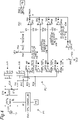
- the current supply circuit includes a primary circuit P1 and a secondary circuit P2.
- the primary circuit P1 includes a power supply 10, a capacitor C11, a transistor TR11, and an inductor L101.
- a resistor R1 and a pulse width modulation (PWM) controller PW are connected to the transistor TR11. Power is supplied from the primary circuit P1 to the secondary circuit P2 via the inductor L101 and an inductor L201 to be described later.
- PWM pulse width modulation
- the secondary circuit P2 includes the inductor L201, two diodes D11, D12, a capacitor C21, four output units L1, L2, L3, L4, and four resistors R11, R12, R13, R14. Power supplied from the primary circuit P1 via the inductor L101 and the inductor L201 is rectified and smoothed via the diodes D11, D12 and the capacitor C21.
- Each output unit L1, L2, L3, L4 has a positive electrode L11 and a negative electrode L12 connected to the external device via the wiring.
- the four resistors R11, R12, R13, R14 are disposed between the positive electrodes L11 and the negative electrodes L12 of the output units L1, L2, L3, L4.
- the four resistors R11, R12, R13, R14 have identical resistance value.
- the secondary circuit P2 includes four operational amplifiers OP21, OP22, OP23, OP24.
- Each of the operational amplifiers OP21, OP22, OP23, OP24 amplifies a voltage of current flowing through corresponding one of resistors R11, R12, R13, R14.
- a noninverting input terminal of the operational amplifier OP1 is connected to the resistor R11 and the negative electrode L12.
- An inverting input terminal of the operational amplifier OP1 is connected to an output terminal of the operational amplifier OP1 and two resistors R21a, R21b.
- the output terminal of the operational amplifier OP1 is connected to a diode D21.
- a noninverting input terminal of the operational amplifier OP2 is connected to the resistor R12 and the negative electrode L12.
- An inverting input terminal of the operational amplifier OP2 is connected to an output terminal of the operational amplifier OP2 and two resistors R22a, R22b.
- the output terminal of the operational amplifier OP2 is connected to a diode D22.
- a noninverting input terminal of the operational amplifier OP3 is connected to the resistor R13 and the negative electrode L12.
- An inverting input terminal of the operational amplifier OP3 is connected to an output terminal of the operational amplifier OP3 and two resistors R23a, R23b.
- the output terminal of the operational amplifier OP3 is connected to a diode D23.
- a noninverting input terminal of the operational amplifier OP4 is connected to the resistor R14 and the negative electrode L12.
- An inverting input terminal of the operational amplifier OP4 is connected to an output terminal of the operational amplifier OP4 and two resistors R24a, R24b.
- the secondary circuit P2 includes four variable resistors R31, R32, R33, R 34, four resistors R41, R42, R43, R44, and four operational amplifiers OP31, OP32, OP33, OP34.
- the variable resistors R31, R32, R33, R34 configure a part of the current setting unit 3.
- a noninverting input terminal of the operational amplifier OP31 is connected to the diode D21.
- An inverting input terminal of the operational amplifier OP31 is connected to the variable resistor R31 and the resistor R41.
- An output terminal of the operational amplifier OP31 is connected to a diode D31.
- a noninverting input terminal of the operational amplifier OP32 is connected to the diode D22.
- An inverting input terminal of the operational amplifier OP32 is connected to the variable resistor R32 and the resistor R42.
- An output terminal of the operational amplifier OP32 is connected to a diode D32.
- a noninverting input terminal of the operational amplifier OP33 is connected to the diode D23.
- An inverting input terminal of the operational amplifier OP33 is connected to the variable resistor R33 and the resistor R43.
- An output terminal of the operational amplifier OP33 is connected to a diode D33.
- a noninverting input terminal of the operational amplifier OP34 is connected to the diode D24.
- An inverting input terminal of the operational amplifier OP34 is connected to the variable resistor R34 and the resistor R44.
- An output terminal of the operational amplifier OP34 is connected to a diode D34.
- Voltages between the variable resistors R31, R32, R33, R34 and the corresponding resistors R41, R42, R43, R44 before being input into the inverting input terminals of the operational amplifiers OP31, OP32, OP33, OP34 are respectively denoted by V31, V32, V33, V34.
- Voltages to be output respectively from the operational amplifiers OP31, OP32, OP33, OP34 are changed in accordance with resistance values of the variable resistors R31, R32, R33, R34.
- the secondary circuit P2 includes a resistor R51, a variable resistor R61, a positive electrode VC1 and a negative electrode VC2 for supplying a constant voltage Vcc, an operational amplifier OP61, a diode D61, a transistor TR21, and a photocoupler PHC1.
- the positive electrode VC1 for supplying the constant voltage Vcc is connected to the resistors R41, R42, R43, R44.
- the constant voltage Vcc is divided by the variable resistors R31, R32, R33, R34 and the resistors R41, R42, R43, R44, thereby obtaining the voltages V31, V32, V33, V34.
- the negative electrode VC2 for supplying the constant voltage Vcc is connected to the variable resistor R61.
- the variable resistor R61 is connected to the four resistors R21b, R22b, R23b, R24b and a noninverting input terminal of the operational amplifier OP61. An inverting input terminal of the operational amplifier OP61 is grounded.
- An output terminal of the operational amplifier OP61 is connected to the diode D61.
- Diodes D31, D32, D33, D34, D61 are connected to the transistor TR21.
- the resistor R51 and the transistor TR21 are connected to the photocoupler PHC1.
- Voltages output from the operational amplifiers OP31, OP32, OP33, OP34 are used as a feedback signal to the primary circuit P1 via the photocoupler PHC1.
- the feedback signal is input to a PWM controller PW.
- the PWM controller PW performs PWM control on voltage of the secondary circuit P2 of the power device 1 based on the feedback signal.
- the current setting unit 3 sets a maximum current to be supplied to an external device via the current supply circuit.
- the current setting unit 3 includes the variable resistor R31, R32, R33, R34 and an operation unit 3a.
- the operation unit 3a is configured to be able to change a resistance value of the variable resistor R31, R32, R33, R34.
- the operation unit 3a is configured by a rotary volume or a slide volume, and is disposed to be adjacent to the hole 2a as illustrated in Fig. 1 .
- the power device 1 can exert the following effects.
- the power device 1 includes a plurality of the terminal blocks 2 electrically connected to each other.
- Each terminal block 2 is configured to be respectively connectable to an external device and to supply current to the connected external device.
- Each terminal block 2 includes a current supply circuit and a current setting unit 3.
- the current supply circuit supplies current to the external device connected to the terminal block 2.
- the current setting unit 3 sets a maximum current to be supplied to the external device via the current supply circuit. With such a configuration, a maximum current to be supplied to each terminal block 2 can be set. Thus, even when one of a plurality of external devices respectively connected to the plurality of terminal blocks 2 via the wiring is broken due to a short circuit, the spread of fire in the wiring connected to the external device broken due to a short circuit can be prevented.
- the current setting unit 3 is disposed in the current supply circuit and includes the variable resistor R31, R32, R33, R34 and the operation unit 3a.
- the resistance value of the variable resistor R31, R32, R33, R34 is changeable.
- the operation unit 3a is capable of changing the resistance value of the variable resistor R31, R32, R33, R34. With such a configuration, a maximum current to be supplied to an external device connected with the terminal block 2 can be easily set.
- the power device 1 can also be configured as follows.
- the current setting unit can use any configuration enabling setting of a maximum current to be supplied to an external devices via the current supply circuit.
- the power device 1 may include a current setting unit 31.
- the current setting unit 31 may be configured to include a plurality of resistors and a selector.
- the plurality of resistors is disposed in parallel to the current supply circuit and has different resistance values to each other.
- the selector is configured to select any one of the plurality of resistors configuring a part of the current supply circuit.
- the power device 1 includes, for example, four set of resistors R301, R302, R303, R304 and four selectors 31b corresponding to the set of resistors R301, R302, R303, R304, respectively.
- Each set of resistors R301, R302, R303, R304 is configured so that a maximum current to be supplied to the connected external device is set to any one of 10 A, 20 A, 30 A, and 40 A, for example.
- the set of resistors R301 is connected to the inverting input terminal of the operational amplifier OP31 and the resistor R41.
- the set of resistors R302 is connected to the inverting input terminal of the operational amplifier OP32 and the resistor R42.
- the set of resistors R303 is connected to the inverting input terminal of the operational amplifier OP33 and the resistor R43.
- the set of resistors R304 is connected to the inverting input terminal of the operational amplifier OP34 and the resistor R44.
- voltages between the resistors R301, R302, R303, R304 and the corresponding resistors R41, R42, R43, R44 before the voltages input into the inverting input terminals of the operational amplifiers OP31, OP32, OP33, OP34 are respectively denoted by V301, V302, V303, V304.
- Each resistor R41, R42, R43, R44 is connected to the positive electrode VC1 for supplying the constant voltage Vcc.
- the constant voltage Vcc is divided by the set of resistors R301, R302, R303, R304 and the resistors R41, R42, R43, R44, thereby obtaining the voltages V301, V302, V303, V304.
- Voltages to be output respectively from the operational amplifiers OP31, OP32, OP33, OP34 are changed in accordance with resistance values of the sets of resistors R301, R302, R303, R304 selected by the selectors 31b.
- the operation unit 31a is configured by, for example, a rotary switch. Rotation of the rotary switch causes a plurality of circuits in which one of the resistors R305, R306, R307, R308 is disposed respectively to be switched via the selector 31b.
- the current setting unit 31 includes the plurality of resistors and the selector 31a.
- the plurality of resistors is disposed in parallel to the current supply circuit and has different resistance values to each other.
- the selector 31b selects any one of the plurality of resistors configuring a part of the current supply circuit. With such a configuration, a maximum current to be supplied to an external device connected with the terminal block 2 can be easily set.
- the power device 1 may include a current setting unit 301.
- the current setting unit 301 may include a voltage setting unit that sets a voltage of current flowing through the current supply circuit, and a control device that controls the voltage setting unit and sets a maximum current to be supplied to an external device.
- the current setting unit 301 includes, for example, four voltage setting units CPU 1, CPU 2, CPU 3, CPU 4, and a the control device 301a.
- An external input device (HID) 401 is connected to the current setting unit 301.
- the external input device 401 is, for example, a rotary encoder.
- the current setting unit 301 and the external input device 401 communicate with each other in a wired or wireless manner.
- the voltage setting unit CPU 1 is connected to the inverting input terminal of the operational amplifier OP31.
- the voltage setting unit CPU 2 is connected to the inverting input terminal of the operational amplifier OP32.
- the voltage setting unit CPU 3 is connected to the inverting input terminal of the operational amplifier OP33.
- the voltage setting unit CPU 4 is connected to the inverting input terminal of the operational amplifier OP34.
- voltages to be input into the inverting input terminals of the operational amplifiers OP31, OP32, OP33, OP34 from the voltage setting units CPU1, CPU2, CPU3, CPU4 are respectively denoted by V321, V322, V323, V324.
- Voltages to be output respectively from the operational amplifiers OP31, OP32, OP33, OP34 are changed in accordance with the voltages set respectively by the voltage setting units CPU1, CPU2, CPU3, CPU4.
- the control device 301a includes, for example, a central processing unit (CPU).
- the control device 301a is configured to store information input from the external input device 401.
- the control device 301a causes the voltage setting units CPU1, CPU2, CPU3, CPU4 to set voltages based on information input by a user through the external input device 401.
- the current setting unit 301 includes the voltage setting unit CPU1, CPU2, CPU3, CPU4 and the control device 301a.
- the voltage setting unit CPU1, CPU2, CPU3, CPU4 sets a voltage of current flowing through the current supply circuit.
- the control device 301a causes the voltage setting unit CPU1, CPU 2, CPU3, CPU4 to control a maximum current to be supplied to the external device. With such a configuration, a maximum current to be supplied to an external device connected with the terminal block 2 can be set in advance without actually outputting an output current.
- a voltage of the secondary circuit P2 of the power device 1 may be controlled not only by the PWM control but also by other methods such as frequency control.
- the power device 1 includes
- the selector 31b includes a switch that switches a plurality of circuits in which one of the plurality of resistors is respectively disposed.
- the power device of the present disclosure is useful for, for example, a switching power supply that simultaneously supplies current to external devices having different rated currents.
Landscapes
- Engineering & Computer Science (AREA)
- Power Engineering (AREA)
- Direct Current Feeding And Distribution (AREA)
- Control Of Voltage And Current In General (AREA)
- Dc-Dc Converters (AREA)
Abstract
A power device (1) includes a plurality of terminal blocks (2) electrically connected to each other. Each of the plurality of terminal blocks (2) is configured to be connectable to an external device and to be capable of supplying current to the connected external device. Each of the plurality of terminal blocks (2) includes a current supply circuit (PI, P2) that supplies current to the connected external device, and a current setting unit (3) that sets a maximum current to be supplied to the external device via the current supply circuit (PI, P2).
Description
- The present disclosure relates to a power device including a plurality of terminal blocks.
-
Patent document 1 discloses a power device having a plurality of output terminal blocks. Each output terminal block supplies a voltage and a current to a load via wiring. - Patent Document 1:
Japanese Patent Application Laid-Open No. 2021-87302 - Generally, in the power device, the output terminal blocks are electrically connected to each other, and a thickness of a wiring is changed in accordance with current to be supplied to the load connected to each output terminal block. For example, in a case where a plurality of loads that respectively is supplied to different currents is connected to the power device, when a load that is connected with wiring having a small diameter is broken due to a short circuit, a current to be supplied to another load may concentrate on the wiring connected to the broken load. When the current to be supplied to the another load concentrate on one wiring, a current flowing through this wiring may exceed an allowable amount, thereby causing a spread of fire in the wiring.
- An object of the present disclosure is to provide a power device capable of preventing spread of fire in wiring connected to an external device broken due to a short circuit when one of a plurality of external devices connected to each terminal block via wiring is broken due to a short circuit.
- A power device according to one aspect of the present disclosure includes
- a plurality of terminal blocks that is electrically connected to each other, each of the plurality of terminal blocks being configured to be connectable to an external device and to be capable of supplying current to the connected external device, wherein
- each of the plurality of terminal blocks includes
- a current supply circuit that supplies current to the connected external device, and
- a current setting unit that sets a maximum current to be supplied to the external device via the current supply circuit.
- The power device according to the above aspect can prevent spread of fire in wiring connected to an external device broken due to a short circuit when one of a plurality of external devices connected to each terminal block via wiring is broken due to a short circuit.
-
-
Fig. 1 is a front view illustrating a power device according to one embodiment of the present disclosure. -
Fig. 2 is a circuit diagram of the power device ofFig. 1 . -
Fig. 3 is a front view illustrating a first modification of the power device ofFig. 1 . -
Fig. 4 is a circuit diagram of the power device ofFig. 3 . -
Fig. 5 is a front view illustrating a second modification of the power device ofFig. 1 . -
Fig. 6 is a circuit diagram of the power device ofFig. 5 . - An embodiment and a modifications of the present disclosure will be described below with reference to the drawings. In the following description, terms (terms including, for example, "upper", "lower", etc.) indicating specific directions or positions are used as necessary, but the use of these terms is to facilitate understanding of the disclosure with reference to the drawings, and the technical scope of the present disclosure is not limited by the meanings of these terms. Further, the following description is essentially an example, and is not intended to limit the present disclosure, its application, or its use. Furthermore, the drawings are schematic, and ratios of dimensions and the like do not necessarily match actual ones.
- As illustrated in
Fig. 1 , apower device 1 according to one exemplary embodiment of the present disclosure includes a plurality ofterminal blocks 2 electrically connected to each other. For example, thepower device 1 shown inFig. 1 includes fiveterminal blocks 2 and uses fourterminal block 2 among five terminal blocks. - Each
terminal block 2 is electrically connected to an external device (not illustrated) via a wiring (not illustrated). Eachterminal block 2 is provided with ahole 2a for accommodating the wiring. The wiring is connected to a secondary circuit P2 of eachterminal block 2 via thehole 2a. Thepower device 1 supplies source power to the external device via theterminal blocks 2 and the wiring. The external device is an example of a load, and includes, for example, a motor or a light emitting diode (LED) lighting device. - The wiring is selected by, for example, an allowable current value corresponding to a magnitude of a rated current of the external device. For example, when the external device is an LED lighting device with a rated current of 1 A (ampere), the wiring of American wire gauge (AWG) 18 is selected. For example, when the external device is motor with a rated current of 37 A, the wiring of AWG 12 is used.
- As illustrated in
Figs. 1 and2 , eachterminal block 2 includes a current supply circuit that supplies a current to a connected external device, and acurrent setting unit 3. - As an example, as illustrated in
Fig. 2 , the current supply circuit includes a primary circuit P1 and a secondary circuit P2. - The primary circuit P1 includes a
power supply 10, a capacitor C11, a transistor TR11, and an inductor L101. A resistor R1 and a pulse width modulation (PWM) controller PW are connected to the transistor TR11. Power is supplied from the primary circuit P1 to the secondary circuit P2 via the inductor L101 and an inductor L201 to be described later. - The secondary circuit P2 includes the inductor L201, two diodes D11, D12, a capacitor C21, four output units L1, L2, L3, L4, and four resistors R11, R12, R13, R14. Power supplied from the primary circuit P1 via the inductor L101 and the inductor L201 is rectified and smoothed via the diodes D11, D12 and the capacitor C21.
- Each output unit L1, L2, L3, L4 has a positive electrode L11 and a negative electrode L12 connected to the external device via the wiring. The four resistors R11, R12, R13, R14 are disposed between the positive electrodes L11 and the negative electrodes L12 of the output units L1, L2, L3, L4. As one example, the four resistors R11, R12, R13, R14 have identical resistance value.
- The secondary circuit P2 includes four operational amplifiers OP21, OP22, OP23, OP24. Each of the operational amplifiers OP21, OP22, OP23, OP24 amplifies a voltage of current flowing through corresponding one of resistors R11, R12, R13, R14.
- In the present embodiment, a noninverting input terminal of the operational amplifier OP1 is connected to the resistor R11 and the negative electrode L12. An inverting input terminal of the operational amplifier OP1 is connected to an output terminal of the operational amplifier OP1 and two resistors R21a, R21b. The output terminal of the operational amplifier OP1 is connected to a diode D21. A noninverting input terminal of the operational amplifier OP2 is connected to the resistor R12 and the negative electrode L12. An inverting input terminal of the operational amplifier OP2 is connected to an output terminal of the operational amplifier OP2 and two resistors R22a, R22b. The output terminal of the operational amplifier OP2 is connected to a diode D22. A noninverting input terminal of the operational amplifier OP3 is connected to the resistor R13 and the negative electrode L12. An inverting input terminal of the operational amplifier OP3 is connected to an output terminal of the operational amplifier OP3 and two resistors R23a, R23b. The output terminal of the operational amplifier OP3 is connected to a diode D23. A noninverting input terminal of the operational amplifier OP4 is connected to the resistor R14 and the negative electrode L12. An inverting input terminal of the operational amplifier OP4 is connected to an output terminal of the operational amplifier OP4 and two resistors R24a, R24b. The output terminal of the operational amplifier OP4 is connected to a diode D24. Voltages of currents, which are amplified by the operational amplifiers OP1, OP2, OP3, OP4, flowing through the resistors R11, R12, R13, R14 are respectively denoted by V1, V2, V3, V4.
- The secondary circuit P2 includes four variable resistors R31, R32, R33, R 34, four resistors R41, R42, R43, R44, and four operational amplifiers OP31, OP32, OP33, OP34. In the embodiment, the variable resistors R31, R32, R33, R34 configure a part of the
current setting unit 3. - In the present embodiment, a noninverting input terminal of the operational amplifier OP31 is connected to the diode D21. An inverting input terminal of the operational amplifier OP31 is connected to the variable resistor R31 and the resistor R41. An output terminal of the operational amplifier OP31 is connected to a diode D31. A noninverting input terminal of the operational amplifier OP32 is connected to the diode D22. An inverting input terminal of the operational amplifier OP32 is connected to the variable resistor R32 and the resistor R42. An output terminal of the operational amplifier OP32 is connected to a diode D32. A noninverting input terminal of the operational amplifier OP33 is connected to the diode D23. An inverting input terminal of the operational amplifier OP33 is connected to the variable resistor R33 and the resistor R43. An output terminal of the operational amplifier OP33 is connected to a diode D33. A noninverting input terminal of the operational amplifier OP34 is connected to the diode D24. An inverting input terminal of the operational amplifier OP34 is connected to the variable resistor R34 and the resistor R44. An output terminal of the operational amplifier OP34 is connected to a diode D34. Voltages between the variable resistors R31, R32, R33, R34 and the corresponding resistors R41, R42, R43, R44 before being input into the inverting input terminals of the operational amplifiers OP31, OP32, OP33, OP34 are respectively denoted by V31, V32, V33, V34. Voltages to be output respectively from the operational amplifiers OP31, OP32, OP33, OP34 are changed in accordance with resistance values of the variable resistors R31, R32, R33, R34.
- The secondary circuit P2 includes a resistor R51, a variable resistor R61, a positive electrode VC1 and a negative electrode VC2 for supplying a constant voltage Vcc, an operational amplifier OP61, a diode D61, a transistor TR21, and a photocoupler PHC1.
- In the present embodiment, the positive electrode VC1 for supplying the constant voltage Vcc is connected to the resistors R41, R42, R43, R44. The constant voltage Vcc is divided by the variable resistors R31, R32, R33, R34 and the resistors R41, R42, R43, R44, thereby obtaining the voltages V31, V32, V33, V34. The negative electrode VC2 for supplying the constant voltage Vcc is connected to the variable resistor R61. The variable resistor R61 is connected to the four resistors R21b, R22b, R23b, R24b and a noninverting input terminal of the operational amplifier OP61. An inverting input terminal of the operational amplifier OP61 is grounded. An output terminal of the operational amplifier OP61 is connected to the diode D61. Diodes D31, D32, D33, D34, D61 are connected to the transistor TR21. The resistor R51 and the transistor TR21 are connected to the photocoupler PHC1. Voltages output from the operational amplifiers OP31, OP32, OP33, OP34 are used as a feedback signal to the primary circuit P1 via the photocoupler PHC1. The feedback signal is input to a PWM controller PW. The PWM controller PW performs PWM control on voltage of the secondary circuit P2 of the
power device 1 based on the feedback signal. - The
current setting unit 3 sets a maximum current to be supplied to an external device via the current supply circuit. In the present embodiment, as illustrated inFigs. 1 and2 , thecurrent setting unit 3 includes the variable resistor R31, R32, R33, R34 and an operation unit 3a. The operation unit 3a is configured to be able to change a resistance value of the variable resistor R31, R32, R33, R34. For example, the operation unit 3a is configured by a rotary volume or a slide volume, and is disposed to be adjacent to thehole 2a as illustrated inFig. 1 . - The
power device 1 can exert the following effects. - The
power device 1 includes a plurality of the terminal blocks 2 electrically connected to each other. Eachterminal block 2 is configured to be respectively connectable to an external device and to supply current to the connected external device. Eachterminal block 2 includes a current supply circuit and acurrent setting unit 3. The current supply circuit supplies current to the external device connected to theterminal block 2. Thecurrent setting unit 3 sets a maximum current to be supplied to the external device via the current supply circuit. With such a configuration, a maximum current to be supplied to eachterminal block 2 can be set. Thus, even when one of a plurality of external devices respectively connected to the plurality ofterminal blocks 2 via the wiring is broken due to a short circuit, the spread of fire in the wiring connected to the external device broken due to a short circuit can be prevented. - The
current setting unit 3 is disposed in the current supply circuit and includes the variable resistor R31, R32, R33, R34 and the operation unit 3a. The resistance value of the variable resistor R31, R32, R33, R34 is changeable. The operation unit 3a is capable of changing the resistance value of the variable resistor R31, R32, R33, R34. With such a configuration, a maximum current to be supplied to an external device connected with theterminal block 2 can be easily set. - The
power device 1 can also be configured as follows. - The current setting unit can use any configuration enabling setting of a maximum current to be supplied to an external devices via the current supply circuit.
- For example, as illustrated in
Figs. 3 and4 , thepower device 1 may include acurrent setting unit 31. Thecurrent setting unit 31 may be configured to include a plurality of resistors and a selector. The plurality of resistors is disposed in parallel to the current supply circuit and has different resistance values to each other. The selector is configured to select any one of the plurality of resistors configuring a part of the current supply circuit. InFigs. 3 and4 , thepower device 1 includes, for example, four set of resistors R301, R302, R303, R304 and fourselectors 31b corresponding to the set of resistors R301, R302, R303, R304, respectively. Each set of resistors R301, R302, R303, R304 is configured so that a maximum current to be supplied to the connected external device is set to any one of 10 A, 20 A, 30 A, and 40 A, for example. - The set of resistors R301 is connected to the inverting input terminal of the operational amplifier OP31 and the resistor R41. The set of resistors R302 is connected to the inverting input terminal of the operational amplifier OP32 and the resistor R42. The set of resistors R303 is connected to the inverting input terminal of the operational amplifier OP33 and the resistor R43. The set of resistors R304 is connected to the inverting input terminal of the operational amplifier OP34 and the resistor R44. In the
power device 1 illustrated inFigs. 3 and4 , voltages between the resistors R301, R302, R303, R304 and the corresponding resistors R41, R42, R43, R44 before the voltages input into the inverting input terminals of the operational amplifiers OP31, OP32, OP33, OP34 are respectively denoted by V301, V302, V303, V304. - Each resistor R41, R42, R43, R44 is connected to the positive electrode VC1 for supplying the constant voltage Vcc. The constant voltage Vcc is divided by the set of resistors R301, R302, R303, R304 and the resistors R41, R42, R43, R44, thereby obtaining the voltages V301, V302, V303, V304. Voltages to be output respectively from the operational amplifiers OP31, OP32, OP33, OP34 are changed in accordance with resistance values of the sets of resistors R301, R302, R303, R304 selected by the
selectors 31b. - The
operation unit 31a is configured by, for example, a rotary switch. Rotation of the rotary switch causes a plurality of circuits in which one of the resistors R305, R306, R307, R308 is disposed respectively to be switched via theselector 31b. - In the
power device 1 illustrated inFigs. 3 and4 , thecurrent setting unit 31 includes the plurality of resistors and theselector 31a. The plurality of resistors is disposed in parallel to the current supply circuit and has different resistance values to each other. Theselector 31b selects any one of the plurality of resistors configuring a part of the current supply circuit. With such a configuration, a maximum current to be supplied to an external device connected with theterminal block 2 can be easily set. - For example, as illustrated in
Figs. 5 and6 , thepower device 1 may include acurrent setting unit 301. Thecurrent setting unit 301 may include a voltage setting unit that sets a voltage of current flowing through the current supply circuit, and a control device that controls the voltage setting unit and sets a maximum current to be supplied to an external device. InFigs. 5 and6 , thecurrent setting unit 301 includes, for example, four voltagesetting units CPU 1,CPU 2,CPU 3, CPU 4, and a thecontrol device 301a. An external input device (HID) 401 is connected to thecurrent setting unit 301. Theexternal input device 401 is, for example, a rotary encoder. Thecurrent setting unit 301 and theexternal input device 401 communicate with each other in a wired or wireless manner. - The voltage
setting unit CPU 1 is connected to the inverting input terminal of the operational amplifier OP31. The voltagesetting unit CPU 2 is connected to the inverting input terminal of the operational amplifier OP32. The voltagesetting unit CPU 3 is connected to the inverting input terminal of the operational amplifier OP33. The voltage setting unit CPU 4 is connected to the inverting input terminal of the operational amplifier OP34. In thepower device 1 illustrated inFigs. 5 and6 , voltages to be input into the inverting input terminals of the operational amplifiers OP31, OP32, OP33, OP34 from the voltage setting units CPU1, CPU2, CPU3, CPU4 are respectively denoted by V321, V322, V323, V324. Voltages to be output respectively from the operational amplifiers OP31, OP32, OP33, OP34 are changed in accordance with the voltages set respectively by the voltage setting units CPU1, CPU2, CPU3, CPU4. - The
control device 301a includes, for example, a central processing unit (CPU). Thecontrol device 301a is configured to store information input from theexternal input device 401. Thecontrol device 301a causes the voltage setting units CPU1, CPU2, CPU3, CPU4 to set voltages based on information input by a user through theexternal input device 401. - In the
power device 1 illustrated inFigs. 5 and6 , thecurrent setting unit 301 includes the voltage setting unit CPU1, CPU2, CPU3, CPU4 and thecontrol device 301a. The voltage setting unit CPU1, CPU2, CPU3, CPU4 sets a voltage of current flowing through the current supply circuit. Thecontrol device 301a causes the voltage setting unit CPU1,CPU 2, CPU3, CPU4 to control a maximum current to be supplied to the external device. With such a configuration, a maximum current to be supplied to an external device connected with theterminal block 2 can be set in advance without actually outputting an output current. - A voltage of the secondary circuit P2 of the
power device 1 may be controlled not only by the PWM control but also by other methods such as frequency control. - Various embodiments of the present disclosure have been described above in detail with reference to the drawings. Finally, various aspects of the present disclosure will be described. In the following description, as an example, reference signs are also added.
- The
power device 1 according to a first aspect of the present disclosure includes - a plurality of
terminal blocks 2 that is electrically connected to each other, each of the plurality ofterminal blocks 2 being configured to be connectable to an external device and to be capable of supplying current to the connected external device, wherein - each of the plurality of
terminal blocks 2 includes - a current supply circuit that supplies current to the connected external device, and
- a
current setting unit 3 that sets a maximum current to be supplied to the external device via the current supply circuit. - In the
power device 1 according to a second aspect of the present disclosure, - the
current setting unit 3 includes - a variable resistor R31, R32, R33, R34 that is disposed in the current supply circuit, a resistance value of the variable resistor being changeable, and
- an operation unit 3a that is capable of changing the resistance value of the variable resistor R31, R32, R33, R34.
- In the
power device 1 according to a third aspect of the present disclosure, - the
current setting unit 31 includes - a plurality of resistors that is disposed in parallel to the current supply circuit and has different resistance values to each other, and
- a
selector 31b that selects any one of the plurality of resistors. - In the
power device 1 according to a fourth aspect of the present disclosure,
theselector 31b includes a switch that switches a plurality of circuits in which one of the plurality of resistors is respectively disposed. - In the
power device 1 according to a fifth aspect of the present disclosure, - the
current setting unit 301 includes - a voltage of current setting unit CPU1, CPU2, CPU3, CPU4 that sets a voltage flowing through the current supply circuit, and
- a
control device 301a that controls the voltage setting unit CPU1,CPU 2, CPU3, CPU4 to set a maximum current to be supplied to the external device. - An appropriate combination of any embodiments or modifications among the various embodiments or modifications described above can achieve the effects of the respective embodiments or modifications. In addition, any embodiments can be combined, any examples can be combined, or any embodiment is combined with any example. Further, features in different embodiments or different examples can be combined.
- The power device of the present disclosure is useful for, for example, a switching power supply that simultaneously supplies current to external devices having different rated currents.
-
- 1 power device
- 10 power supply
- 2 terminal block
- 2a hole
- 3, 31, 301 current setting unit
- 3a, 31a operation unit
- 31b selector
- 301a control device
- 401 external input unit
- C11, C21 capacitor
- CPU1, CPU2, CPU3, CPU4 voltage setting unit
- D11, D12, D21, D22, D23, D24, D31, D32, D33, D34, D61 diode
- OP21, OP22, OP23, OP24, OP31, OP32, OP33, OP34, OP61 operational amplifier
- P1 primary circuit
- P2 secondary circuit
- PHC1 photocoupler
- PW PWM controller
- R1, R11, R12, R13, R14, R21a, R22a, R23a, R24a, R21b, R22b, R23b, R24b, R41, R42, R43, R44, R51, R305, R306, R307, R308 resistor
- R31, R32, R33, R34, R61 variable resistor
- R301, R302, R303, R304 set of resistors
- TR11, TR21 transistor
Claims (5)
- A power device (1) characterized by comprising:a plurality of terminal blocks (2) that is electrically connected to each other, each of the plurality of terminal blocks being configured to be connectable to an external device and to be capable of supplying current to the connected external device, whereineach of the plurality of terminal blocks (2) includesa current supply circuit (P1, P2) that supplies current to the connected external device, anda current setting unit (3) that sets a maximum current to be supplied to the external device via the current supply circuit.
- The power device (1) according to claim 1, whereinthe current setting unit (3) includesa variable resistor (R31,R32,R33,R34) that is disposed in the current supply circuit (P1, P2), a resistance value of the variable resistor (R31,R32,R33,R34) being changeable, andan operation unit (3a) that is capable of changing the resistance value of the variable resistor (R31,R32,R33,R34).
- The power device according to claim 1, whereinthe current setting unit (31) includesa plurality of resistors (R305, R306, R307, R308) that is disposed in parallel to the current supply circuit (p1, p2) and has different resistance values to each other, anda selector (31a) that selects any one of the plurality of resistors (R305, R306, R307, R308).
- The power device (1) according to claim 3, wherein
the selector (31a) includes a switch that switches a plurality of circuits in which one of the plurality of resistors (R305, R306, R307, R308) is respectively disposed. - The power device (1) according to claim 1, whereinthe current setting unit (301) includesa voltage setting unit (CPU1, CPU2, CPU3, CPU4) that sets a voltage of current flowing through the current supply circuit (P1, P2), anda control device (301a) that controls the voltage setting unit (CPU1, CPU2, CPU3, CPU4) to set a maximum current to be supplied to the external device.
Applications Claiming Priority (1)
| Application Number | Priority Date | Filing Date | Title |
|---|---|---|---|
| JP2021114415A JP2023010341A (en) | 2021-07-09 | 2021-07-09 | Power supply device |
Publications (1)
| Publication Number | Publication Date |
|---|---|
| EP4117130A1 true EP4117130A1 (en) | 2023-01-11 |
Family
ID=82492755
Family Applications (1)
| Application Number | Title | Priority Date | Filing Date |
|---|---|---|---|
| EP22181803.2A Withdrawn EP4117130A1 (en) | 2021-07-09 | 2022-06-29 | Power device |
Country Status (4)
| Country | Link |
|---|---|
| US (1) | US20230010478A1 (en) |
| EP (1) | EP4117130A1 (en) |
| JP (1) | JP2023010341A (en) |
| CN (1) | CN115603554A (en) |
Citations (3)
| Publication number | Priority date | Publication date | Assignee | Title |
|---|---|---|---|---|
| JPH06276673A (en) * | 1993-03-15 | 1994-09-30 | Sumitomo Electric Ind Ltd | Circuit for limiting rush current |
| US20040201931A1 (en) * | 2002-10-14 | 2004-10-14 | Dror Korcharz | Configurable multiple power source system |
| JP2021087302A (en) | 2019-11-28 | 2021-06-03 | コーセル株式会社 | Power supply device |
Family Cites Families (10)
| Publication number | Priority date | Publication date | Assignee | Title |
|---|---|---|---|---|
| US4949214A (en) * | 1989-08-28 | 1990-08-14 | Spencer George A | Trip delay override for electrical circuit breakers |
| JP4984341B2 (en) * | 1999-08-04 | 2012-07-25 | 株式会社デンソー | Display device |
| US7895456B2 (en) * | 2006-11-12 | 2011-02-22 | Microsemi Corp. - Analog Mixed Signal Group Ltd | Reduced guard band for power over Ethernet |
| US8368379B2 (en) * | 2010-03-04 | 2013-02-05 | Maxim Integrated Products, Inc. | Apparatus and method for monitoring output within a power strip |
| US8610421B2 (en) * | 2010-12-22 | 2013-12-17 | Taiwan Semiconductor Manufacturing Company, Ltd. | Current generator and method of operating |
| CN102609065A (en) * | 2011-01-19 | 2012-07-25 | 鸿富锦精密工业(深圳)有限公司 | Over-current protection device |
| CN205882313U (en) * | 2016-07-04 | 2017-01-11 | 富欣实业股份有限公司 | Outlet System for Wireless Power Monitoring |
| CN108270130B (en) * | 2017-12-29 | 2020-11-27 | 成都觅瑞科技有限公司 | Socket and power supply system |
| CN109326930A (en) * | 2018-11-08 | 2019-02-12 | 国网黑龙江省电力有限公司信息通信公司 | Computer room power socket with power-off protection and reminder and power-off protection and reminder method of the socket |
| CN112787133B (en) * | 2019-11-06 | 2023-01-24 | 智慧式控股有限公司 | Mobile socket board with plug power-off, electric shock prevention and electric fire hazard monitoring functions |
-
2021
- 2021-07-09 JP JP2021114415A patent/JP2023010341A/en active Pending
-
2022
- 2022-06-29 CN CN202210748357.2A patent/CN115603554A/en active Pending
- 2022-06-29 EP EP22181803.2A patent/EP4117130A1/en not_active Withdrawn
- 2022-07-08 US US17/860,356 patent/US20230010478A1/en not_active Abandoned
Patent Citations (3)
| Publication number | Priority date | Publication date | Assignee | Title |
|---|---|---|---|---|
| JPH06276673A (en) * | 1993-03-15 | 1994-09-30 | Sumitomo Electric Ind Ltd | Circuit for limiting rush current |
| US20040201931A1 (en) * | 2002-10-14 | 2004-10-14 | Dror Korcharz | Configurable multiple power source system |
| JP2021087302A (en) | 2019-11-28 | 2021-06-03 | コーセル株式会社 | Power supply device |
Also Published As
| Publication number | Publication date |
|---|---|
| JP2023010341A (en) | 2023-01-20 |
| CN115603554A (en) | 2023-01-13 |
| US20230010478A1 (en) | 2023-01-12 |
Similar Documents
| Publication | Publication Date | Title |
|---|---|---|
| EP1461980B1 (en) | Light emitting diode driver | |
| JP6445558B2 (en) | Power over Ethernet control system | |
| US9681512B1 (en) | Combined wireless voltage controlled dimming interface for an LED driver | |
| JP6471156B2 (en) | Power line communication for lighting systems | |
| JP2015057867A (en) | Bleeder circuit | |
| EP4117130A1 (en) | Power device | |
| KR101422338B1 (en) | Dimming Circuit For LED Lighting Apparatus | |
| WO2018155708A1 (en) | Control device | |
| US20040119339A1 (en) | Adaptive power supply system with multiple input voltages | |
| JP2851730B2 (en) | Programmable controller | |
| KR102768450B1 (en) | Variable Power Capacity Dimming Converter | |
| EP3095301B1 (en) | A circuit arrangement for operating led strings | |
| US6169491B1 (en) | Multiport power monitor | |
| JP6728299B2 (en) | Three-stage switching type omnidirectional LED lamp drive circuit | |
| JP2015506104A (en) | Light emitting device and system | |
| EP3949689B1 (en) | Power supply configuration across isolation barrier | |
| EP1656001A1 (en) | Flashing lights control apparatus and method thereof | |
| CN218735080U (en) | External power regulating circuit and device and constant current driving equipment | |
| CN203193996U (en) | Circuit arrangement for operating at least one discharge lamp | |
| EP4637269A1 (en) | Driver system for supplying an led load with a dc voltage | |
| TWI450639B (en) | Methods and apparatus for driving led-based lighting units | |
| CN115278977A (en) | Three-in-one dimming power supply cascade control circuit with external adjustable resistor | |
| JP6563315B2 (en) | LED controller | |
| WO2022248256A1 (en) | Powering by a fieldbus during logic low signal level | |
| CN104967289B (en) | Switch controller and its application |
Legal Events
| Date | Code | Title | Description |
|---|---|---|---|
| PUAI | Public reference made under article 153(3) epc to a published international application that has entered the european phase |
Free format text: ORIGINAL CODE: 0009012 |
|
| STAA | Information on the status of an ep patent application or granted ep patent |
Free format text: STATUS: REQUEST FOR EXAMINATION WAS MADE |
|
| 17P | Request for examination filed |
Effective date: 20220629 |
|
| AK | Designated contracting states |
Kind code of ref document: A1 Designated state(s): AL AT BE BG CH CY CZ DE DK EE ES FI FR GB GR HR HU IE IS IT LI LT LU LV MC MK MT NL NO PL PT RO RS SE SI SK SM TR |
|
| STAA | Information on the status of an ep patent application or granted ep patent |
Free format text: STATUS: THE APPLICATION IS DEEMED TO BE WITHDRAWN |
|
| 18D | Application deemed to be withdrawn |
Effective date: 20230712 |