EP4117048A1 - Electrolyte-based field effect transistor and associated method of fabrication - Google Patents
Electrolyte-based field effect transistor and associated method of fabrication Download PDFInfo
- Publication number
- EP4117048A1 EP4117048A1 EP21184370.1A EP21184370A EP4117048A1 EP 4117048 A1 EP4117048 A1 EP 4117048A1 EP 21184370 A EP21184370 A EP 21184370A EP 4117048 A1 EP4117048 A1 EP 4117048A1
- Authority
- EP
- European Patent Office
- Prior art keywords
- electrolyte
- electrode
- layer
- source
- drain
- Prior art date
- Legal status (The legal status is an assumption and is not a legal conclusion. Google has not performed a legal analysis and makes no representation as to the accuracy of the status listed.)
- Withdrawn
Links
Images



Classifications
-
- H—ELECTRICITY
- H10—SEMICONDUCTOR DEVICES; ELECTRIC SOLID-STATE DEVICES NOT OTHERWISE PROVIDED FOR
- H10N—ELECTRIC SOLID-STATE DEVICES NOT OTHERWISE PROVIDED FOR
- H10N70/00—Solid-state devices having no potential barriers, and specially adapted for rectifying, amplifying, oscillating or switching
- H10N70/20—Multistable switching devices, e.g. memristors
- H10N70/253—Multistable switching devices, e.g. memristors having three or more electrodes, e.g. transistor-like devices
-
- G—PHYSICS
- G01—MEASURING; TESTING
- G01N—INVESTIGATING OR ANALYSING MATERIALS BY DETERMINING THEIR CHEMICAL OR PHYSICAL PROPERTIES
- G01N27/00—Investigating or analysing materials by the use of electric, electrochemical, or magnetic means
- G01N27/26—Investigating or analysing materials by the use of electric, electrochemical, or magnetic means by investigating electrochemical variables; by using electrolysis or electrophoresis
- G01N27/403—Cells and electrode assemblies
- G01N27/414—Ion-sensitive or chemical field-effect transistors, i.e. ISFETS or CHEMFETS
-
- H—ELECTRICITY
- H10—SEMICONDUCTOR DEVICES; ELECTRIC SOLID-STATE DEVICES NOT OTHERWISE PROVIDED FOR
- H10D—INORGANIC ELECTRIC SEMICONDUCTOR DEVICES
- H10D30/00—Field-effect transistors [FET]
- H10D30/01—Manufacture or treatment
- H10D30/021—Manufacture or treatment of FETs having insulated gates [IGFET]
- H10D30/031—Manufacture or treatment of FETs having insulated gates [IGFET] of thin-film transistors [TFT]
-
- H—ELECTRICITY
- H10—SEMICONDUCTOR DEVICES; ELECTRIC SOLID-STATE DEVICES NOT OTHERWISE PROVIDED FOR
- H10D—INORGANIC ELECTRIC SEMICONDUCTOR DEVICES
- H10D30/00—Field-effect transistors [FET]
- H10D30/60—Insulated-gate field-effect transistors [IGFET]
- H10D30/67—Thin-film transistors [TFT]
- H10D30/6758—Thin-film transistors [TFT] characterised by the insulating substrates
-
- H—ELECTRICITY
- H10—SEMICONDUCTOR DEVICES; ELECTRIC SOLID-STATE DEVICES NOT OTHERWISE PROVIDED FOR
- H10N—ELECTRIC SOLID-STATE DEVICES NOT OTHERWISE PROVIDED FOR
- H10N70/00—Solid-state devices having no potential barriers, and specially adapted for rectifying, amplifying, oscillating or switching
- H10N70/011—Manufacture or treatment of multistable switching devices
-
- H—ELECTRICITY
- H10—SEMICONDUCTOR DEVICES; ELECTRIC SOLID-STATE DEVICES NOT OTHERWISE PROVIDED FOR
- H10N—ELECTRIC SOLID-STATE DEVICES NOT OTHERWISE PROVIDED FOR
- H10N70/00—Solid-state devices having no potential barriers, and specially adapted for rectifying, amplifying, oscillating or switching
- H10N70/20—Multistable switching devices, e.g. memristors
- H10N70/24—Multistable switching devices, e.g. memristors based on migration or redistribution of ionic species, e.g. anions, vacancies
-
- H—ELECTRICITY
- H10—SEMICONDUCTOR DEVICES; ELECTRIC SOLID-STATE DEVICES NOT OTHERWISE PROVIDED FOR
- H10N—ELECTRIC SOLID-STATE DEVICES NOT OTHERWISE PROVIDED FOR
- H10N70/00—Solid-state devices having no potential barriers, and specially adapted for rectifying, amplifying, oscillating or switching
- H10N70/801—Constructional details of multistable switching devices
- H10N70/881—Switching materials
-
- H—ELECTRICITY
- H10—SEMICONDUCTOR DEVICES; ELECTRIC SOLID-STATE DEVICES NOT OTHERWISE PROVIDED FOR
- H10N—ELECTRIC SOLID-STATE DEVICES NOT OTHERWISE PROVIDED FOR
- H10N70/00—Solid-state devices having no potential barriers, and specially adapted for rectifying, amplifying, oscillating or switching
- H10N70/801—Constructional details of multistable switching devices
- H10N70/881—Switching materials
- H10N70/883—Oxides or nitrides
Definitions
- the technical field of the invention is the one of synaptic transistors.
- the invention concerns a synaptic transistor comprising an electrolyte and more precisely an electrolyte-based synaptic transistor.
- Synaptic transistors are usually based on one of the two following technologies: electric-double-layer transistor or red-ox transistor.
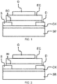
- an electric double layer transistor comprises a dielectric layer OX, a source electrode S and a drain electrode D located on top of the dielectric layer OX, a semi-conductor layer SC on top of the dielectric layer OX and between the source S and the drain D in which is formed the channel of the transistor. It also comprises, on top of the structure already described an electrolyte layer EC and a gate electrode G on top of the electrolyte layer. When a potential is applied to the gate electrode G, charges will move inside the electrolyte EC and produce an electric field in the semi-conductor layer SC located between the source electrode S and the drain electrode D.
- the advantages of such a transistor are a wide conductance range, a high on/off ratio and a high endurance.
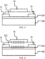
- a red-ox transistor comprises a dielectric layer OX, a source electrode S and a drain electrode D located on top of the dielectric layer OX, an intercalation layer IM on top of the dielectric layer OX and between the source S and the drain D. It also comprises, on top of the structure already described an electrolyte layer EC and a gate electrode G on top of the electrolyte layer EC. When a potential is applied to the gate electrode G, charges will move inside the electrolyte EC and produce a redox reaction between said electrolyte EC and the intercalation layer IM located between the source electrode S and the drain electrode D.
- the advantages of such a transistor are a low working voltage and a three terminals structure. But such a red-ox transistor usually has a low conductance range, a low on/off ratio and a low endurance (compare to the electric double layer transistor). An example of such a transistor is given in US 9,653,159 B2 .
- an electrolyte-based field effect transistor comprising:
- the electrolyte-based transistor according to the invention further comprises:
- the transistor according to the first aspect of the invention may also have one or more of the following characteristics, considered individually or according to any technically possible combinations thereof
- the material of the electrolyte layer comprises lithium phosphorous oxynitride.
- the dielectric material of the dielectric layer has an energy band gap higher than 8 eV.
- the distance between the source electrode and the drain electrode is between 1.5 ⁇ m and 5 ⁇ m.
- the width of the source electrode and the drain electrode (along a direction perpendicular to an axis going through the center of the first electrode and the second electrode) is between 8 ⁇ m and 15 ⁇ m, preferably 10 ⁇ m.
- the thickness of the source electrode, the drain electrode and/or the gate electrode is between 200 nm and 400 nm, preferably 300 nm.
- the thickness of the dielectric layer is between 400 nm and 600 nm, preferably 500 nm.
- the thickness of the electrolyte layer is between 10 nm and 300 nm, preferably 200 nm.
- a second aspect of the invention concerns a spiking neural network comprising a plurality of electrolyte-based field effect transistors according to the invention.
- a third aspect of the invention relates to a method for fabricating an electrolyte-based field effect transistor, said method starting from a substrate and comprising:
- the material of the dielectric layer is the silicon oxide and the step of full-sheet deposition of a dielectric layer on the substrate is implemented using a thermal growth.
- a first aspect of the invention illustrated in figures 3 to 5 concerns an electrolyte-based field effect transistor comprising a dielectric layer OX, a source electrode S and a drain electrode D located on top of the dielectric layer OX.
- the dielectric material of the dielectric layer has an energy band gap higher than 8 eV.
- the distance between the source electrode S and the drain electrode D is between 1.5 ⁇ m and 5 ⁇ m.
- the width of the source electrode S and the drain electrode D (i.e, measured along a direction perpendicular to an axis going through the center of the source electrode S and the drain electrode D) is between 8 ⁇ m and 15 ⁇ m, preferably 10 ⁇ m.
- the thickness of the dielectric layer OX is between 400 nm and 600 nm, preferably 500 nm.
- the material of the dielectric layer OX comprises SiO 2 or any insulating metal oxide such as Al 2 O 3 .
- the electrolyte-based transistor according to the invention further comprises an electrolyte layer EC between and on top of the source electrode S and the drain electrode D, the part of the electrolyte layer located between the source electrode S and the drain electrode D being in direct contact with the dielectric layer OX.
- the electrolyte material of the electrolyte layer EC comprises lithium phosphorous oxynitride.
- the thickness of the electrolyte layer EC is comprised between 10 nm and 300 nm, preferably 200 nm. In an embodiment, when the thickness if not uniform, the thickness of the electrolyte layer EC relates to the thickness of the electrolyte layer EC between the source electrode S and the drain electrode D.
- the electrolyte-based transistor according to the invention also comprises a gate electrode G on top of the electrolyte layer EC, the orthogonal projection of said gate electrode G in a plane comprising the source electrode S and drain electrode D being located, at least in part, between the source electrode S and the drain electrode D.
- the thickness of the source electrode S, the drain electrode D and/or the gate electrode G is between 200 nm and 400 nm, preferably 300 nm.
- a third aspect of the invention illustrated in figures 6A-E and figure 7 concerns a method 100 for fabricating a electrolyte-based field effect transistor, said method starting from a substrate SB.
- the method according to an invention comprises a step E1 of full-sheet deposition of a dielectric layer OX on the substrate.
- the thickness of the dielectric layer OX is between 400 nm and 600 nm, preferably 500 nm.
- This step E1 is followed by a step E2 of full-sheet deposition of a first conductive layer CL on the dielectric layer OX.
- the thickness of the conducive layer CL is between 200 nm and 400 nm, preferably 300 nm.
- the method 100 further comprises a step E3 of patterning the first conductive layer CL to form a source electrode S and a drain electrode D in said conductive layer CL.
- the method 100 also comprises a step E4 of full-sheet deposition of an electrolyte layer EC, the thickness of said electrolyte layer EC being chosen so as to cover the source S and drain D electrodes formed during the preceding step E3.
- the thickness of the electrolyte layer EC is between 10 nm and 300 nm, preferably 200 nm.
- the method 100 further comprises a step E5 of deposition of a second conductive layer CL2 on the electrolyte EC.
- the thickness of the second conducive layer CL2 is between 200 nm and 400 nm, preferably 300 nm.
- this step E5 is followed by a step E6 of patterning the second conductive layer CL2 to form a gate electrode G, the orthogonal projection of said gate electrode G in a plane comprising the source electrode S and drain electrode D being located, at least in part, between the source electrode S and the drain electrode D.
- the inventors were able to verify that it can be used as a transistor, for instance acting as a neuron in a neural network.
- the figure 8 shows the evolution of the source drain current as a function of the source drain voltage for different value of the gate voltage (from 1V to 5V). The modulation of the current when applying voltages on the different electrodes of the transistors.
- the figure 9 shows the evolution of the conductance between the source electrode and the drain electrode as a function of the gate voltage for different distances between the source electrode and the drain electrode. The dependence of the current with respect to the distance between the source electrode and the drain electrode is clearly visible.
- the figure 10 shows the evolution of the conductance in time after voltage pulses of different amplitude (1V, 2V, 3V and 4V) and a duration of 0.5 second applied to the gate.
- the measurement clearly shows a high on/off ratio (up to 525) and a fast relaxation of the conductance after the pulse.
- the figure 11 shows, in red the hysteresis of the source-drain current as a function of the gate voltage and, in blue the hysteresis of the gate current as a function of the gate voltage.
- the measurement clearly shows the decorrelation between the source-drain current and the gate current.
- the figure 12A shows the evolution of the paired-pulse facilitation aka PPF (which corresponds to a synapse property) as a function of the width of the pulse (see figure 12B ).
- the figure 12B shows one measurement that allows to extract the PPF for a given pulse width. This measurement is known of the skilled person and will not be detailed further.
- a transistor according to the invention display features that are characteristics of a field effect transistor and that are compatible with the use in emulating the synaptic plasticity.
Landscapes
- Chemical & Material Sciences (AREA)
- Health & Medical Sciences (AREA)
- Life Sciences & Earth Sciences (AREA)
- Engineering & Computer Science (AREA)
- Physics & Mathematics (AREA)
- Molecular Biology (AREA)
- Chemical Kinetics & Catalysis (AREA)
- Electrochemistry (AREA)
- Microelectronics & Electronic Packaging (AREA)
- Analytical Chemistry (AREA)
- Biochemistry (AREA)
- General Health & Medical Sciences (AREA)
- General Physics & Mathematics (AREA)
- Immunology (AREA)
- Pathology (AREA)
- Manufacturing & Machinery (AREA)
- Thin Film Transistor (AREA)
Abstract
An aspect of the invention concerns a electrolyte-based field effect transistor comprising: a dielectric layer; a source electrode and a drain electrode located on top of the dielectric layer; the electrolyte-based transistor further comprising : an electrolyte layer between and on top of the source electrode and the drain electrode, the part of the electrolyte layer located between the source electrode and the drain electrode being in direct contact with the dielectric layer; and a gate electrode on top of the electrolyte layer, the orthogonal projection of said gate electrode in a plane comprising the source and drain electrodes being located, at least in part, between the source and the drain electrodes.
Description
- The technical field of the invention is the one of synaptic transistors.
- The invention concerns a synaptic transistor comprising an electrolyte and more precisely an electrolyte-based synaptic transistor.
- Synaptic transistors are usually based on one of the two following technologies: electric-double-layer transistor or red-ox transistor.
- As illustrated in
figure 1 , an electric double layer transistor comprises a dielectric layer OX, a source electrode S and a drain electrode D located on top of the dielectric layer OX, a semi-conductor layer SC on top of the dielectric layer OX and between the source S and the drain D in which is formed the channel of the transistor. It also comprises, on top of the structure already described an electrolyte layer EC and a gate electrode G on top of the electrolyte layer. When a potential is applied to the gate electrode G, charges will move inside the electrolyte EC and produce an electric field in the semi-conductor layer SC located between the source electrode S and the drain electrode D. The advantages of such a transistor are a wide conductance range, a high on/off ratio and a high endurance. But an electric double layer transistor usually requires a large working voltage or the use of four terminals (the fourth one being a back gate in addition to the source S, drain D and gate G electrodes). An example of such a transistor is given inUS 10,823,697 B2 - As illustrated in
figure 2 , a red-ox transistor comprises a dielectric layer OX, a source electrode S and a drain electrode D located on top of the dielectric layer OX, an intercalation layer IM on top of the dielectric layer OX and between the source S and the drain D. It also comprises, on top of the structure already described an electrolyte layer EC and a gate electrode G on top of the electrolyte layer EC. When a potential is applied to the gate electrode G, charges will move inside the electrolyte EC and produce a redox reaction between said electrolyte EC and the intercalation layer IM located between the source electrode S and the drain electrode D. The advantages of such a transistor are a low working voltage and a three terminals structure. But such a red-ox transistor usually has a low conductance range, a low on/off ratio and a low endurance (compare to the electric double layer transistor). An example of such a transistor is given inUS 9,653,159 B2 - Therefore, there is a need for a transistor that would possess the advantages of the two types of transistors that were just described but none of their drawbacks.
- According to a first aspect of the invention, this need is satisfied by providing an electrolyte-based field effect transistor comprising:
- a dielectric layer;
- a source electrode and a drain electrode located on top of the dielectric layer.
- The electrolyte-based transistor according to the invention further comprises:
- an electrolyte layer between and on top of the source electrode and the drain electrode, the part of the electrolyte layer located between the source electrode and the drain electrode being in direct contact with the dielectric layer;
- a gate electrode on top of the electrolyte layer, the orthogonal projection of said gate electrode in a plane comprising the source and drain electrodes being located, at least in part, between the source and the drain electrodes.
- The measures performed on such a transistor have shown that it displays a low working voltage, a high on/off ratio, wide conductance range and a high endurance. Furthermore, it operates in a three terminals configuration structure and with low working voltage.
- The transistor according to the first aspect of the invention may also have one or more of the following characteristics, considered individually or according to any technically possible combinations thereof
- In an embodiment the material of the electrolyte layer comprises lithium phosphorous oxynitride.
- In an embodiment, the dielectric material of the dielectric layer has an energy band gap higher than 8 eV.
- In an embodiment, the distance between the source electrode and the drain electrode is between 1.5 µm and 5 µm.
- In an embodiment, the width of the source electrode and the drain electrode (along a direction perpendicular to an axis going through the center of the first electrode and the second electrode) is between 8 µm and 15 µm, preferably 10 µm.
- In an embodiment, the thickness of the source electrode, the drain electrode and/or the gate electrode is between 200 nm and 400 nm, preferably 300 nm.
- In an embodiment, the thickness of the dielectric layer is between 400 nm and 600 nm, preferably 500 nm.
- In an embodiment, the thickness of the electrolyte layer is between 10 nm and 300 nm, preferably 200 nm.
- A second aspect of the invention concerns a spiking neural network comprising a plurality of electrolyte-based field effect transistors according to the invention.
- A third aspect of the invention relates to a method for fabricating an electrolyte-based field effect transistor, said method starting from a substrate and comprising:
- A step of full-sheet deposition of a dielectric layer on the substrate;
- A step of full-sheet deposition of a first conductive layer on the dielectric layer;
- A step of patterning the first conductive layer to form a source electrode and a drain electrode in said conductive layer;
- A step of full-sheet deposition of an electrolyte layer, the thickness of said electrolyte layer being chosen to cover the source and drain electrodes formed during the preceding step;
- A step of deposition of a second conductive layer on the electrolyte layer;
- A step of patterning the second conductive layer to form a gate electrode, the orthogonal projection of said gate electrode in a plane comprising the source and drain electrodes being located, at least in part, between the source and the drain electrodes.
- In an embodiment, the material of the dielectric layer is the silicon oxide and the step of full-sheet deposition of a dielectric layer on the substrate is implemented using a thermal growth.
- Other characteristics and advantages of the invention will become clear from the description that is given thereof below, by way of indication and in no way limiting, with reference to the appended figures.
- The
figure 1 illustrates an electric double layer transistor of the prior art. - The
figure 2 illustrates a red-ox transistor of the prior art. - The
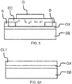
figures 3 to 5 illustrate an electrolyte-based transistor according to the invention. - The
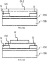
figures 6A to 6E illustrate a method of fabrication according to the invention. - The
figure 7 illustrates a logogram of the method of fabrication according to the invention. - The
figure 8 shows the evolution of the source drain current as a function of the source drain voltage for different value of the gate voltage. - The
figure 9 shows the evolution of the conductance between the source electrode and the drain electrode as a function of the gate voltage for different distance between the source electrode and the drain electrode. - The
figure 10 shows the evolution of the conductance in time after voltage pulses of different amplitude (1V, 2V, 3V and 4V) and a duration of 0.5 second applied to the gate electrode. - The
figure 11 shows, in red the hysteresis of the source-drain current as a function of the gate voltage and, in blue the hysteresis of the gate current as a function of the gate voltage. - The
figure 12A shows the evolution of the paired-pulse facilitation as a function of the width of the pulse. - The
figure 12B shows one measurement that allows to extract the PPF for a given pulse width. - For greater clarity, identical or similar elements are marked by identical reference signs in all the figures.
- A first aspect of the invention illustrated in
figures 3 to 5 concerns an electrolyte-based field effect transistor comprising a dielectric layer OX, a source electrode S and a drain electrode D located on top of the dielectric layer OX. In an embodiment, the dielectric material of the dielectric layer has an energy band gap higher than 8 eV. In an embodiment, the distance between the source electrode S and the drain electrode D is between 1.5 µm and 5 µm. In an embodiment, the width of the source electrode S and the drain electrode D (i.e, measured along a direction perpendicular to an axis going through the center of the source electrode S and the drain electrode D) is between 8 µm and 15 µm, preferably 10 µm. In an embodiment, the thickness of the dielectric layer OX is between 400 nm and 600 nm, preferably 500 nm. In an embodiment, the material of the dielectric layer OX comprises SiO2 or any insulating metal oxide such as Al2O3. - The electrolyte-based transistor according to the invention further comprises an electrolyte layer EC between and on top of the source electrode S and the drain electrode D, the part of the electrolyte layer located between the source electrode S and the drain electrode D being in direct contact with the dielectric layer OX. In particular, there is no semi-conductor layer between the source S and the drain D electrodes in the electrolyte-based field effect transistor according to the invention. In an embodiment, the electrolyte material of the electrolyte layer EC comprises lithium phosphorous oxynitride. In an embodiment, the thickness of the electrolyte layer EC is comprised between 10 nm and 300 nm, preferably 200 nm. In an embodiment, when the thickness if not uniform, the thickness of the electrolyte layer EC relates to the thickness of the electrolyte layer EC between the source electrode S and the drain electrode D.
- The electrolyte-based transistor according to the invention also comprises a gate electrode G on top of the electrolyte layer EC, the orthogonal projection of said gate electrode G in a plane comprising the source electrode S and drain electrode D being located, at least in part, between the source electrode S and the drain electrode D. In an embodiment, the thickness of the source electrode S, the drain electrode D and/or the gate electrode G is between 200 nm and 400 nm, preferably 300 nm.
- As shown in
figure 4 , when a voltage is applied to the gate voltage, charges are formed at the gate/electrolyte interface and at the electrolyte/dielectric interface. Those charges are believed to play a role in the transport properties of the transistor according to the invention. As shown infigure 5 , when the gate voltage is brought back to zero, the charges vanish. The measures performed on such a transistor (seefigures 10 to 13 described later) have shown that it displays a low working voltage, a high on/off ratio, wide conductance range and a high endurance. Furthermore, it operates in a three terminals configuration structure and with low working voltage and can be used in a spiking neural network to obtain a spiking neural network according to a second aspect of the invention. - A third aspect of the invention illustrated in
figures 6A-E andfigure 7 concerns amethod 100 for fabricating a electrolyte-based field effect transistor, said method starting from a substrate SB. - The method according to an invention comprises a step E1 of full-sheet deposition of a dielectric layer OX on the substrate. In an embodiment, the thickness of the dielectric layer OX is between 400 nm and 600 nm, preferably 500 nm.
- This step E1 is followed by a step E2 of full-sheet deposition of a first conductive layer CL on the dielectric layer OX. In an embodiment, the thickness of the conducive layer CL is between 200 nm and 400 nm, preferably 300 nm.
- The structure obtained after these two steps E1-E2 is illustrated in
figure 6A . - As illustrated in
figure 6B , themethod 100 further comprises a step E3 of patterning the first conductive layer CL to form a source electrode S and a drain electrode D in said conductive layer CL. - As illustrated in
figure 6C , themethod 100 also comprises a step E4 of full-sheet deposition of an electrolyte layer EC, the thickness of said electrolyte layer EC being chosen so as to cover the source S and drain D electrodes formed during the preceding step E3. In an embodiment, the thickness of the electrolyte layer EC is between 10 nm and 300 nm, preferably 200 nm. - As illustrated in
figure 6D , themethod 100 further comprises a step E5 of deposition of a second conductive layer CL2 on the electrolyte EC. In an embodiment, the thickness of the second conducive layer CL2 is between 200 nm and 400 nm, preferably 300 nm. - As illustrated in
figure 6E , this step E5 is followed by a step E6 of patterning the second conductive layer CL2 to form a gate electrode G, the orthogonal projection of said gate electrode G in a plane comprising the source electrode S and drain electrode D being located, at least in part, between the source electrode S and the drain electrode D. - While the underlying mechanism of the current flowing though the transistor according to the invention is not fully understood, the inventors were able to verify that it can be used as a transistor, for instance acting as a neuron in a neural network.
- The
figure 8 shows the evolution of the source drain current as a function of the source drain voltage for different value of the gate voltage (from 1V to 5V). The modulation of the current when applying voltages on the different electrodes of the transistors. - The
figure 9 shows the evolution of the conductance between the source electrode and the drain electrode as a function of the gate voltage for different distances between the source electrode and the drain electrode. The dependence of the current with respect to the distance between the source electrode and the drain electrode is clearly visible. - The
figure 10 shows the evolution of the conductance in time after voltage pulses of different amplitude (1V, 2V, 3V and 4V) and a duration of 0.5 second applied to the gate. The measurement clearly shows a high on/off ratio (up to 525) and a fast relaxation of the conductance after the pulse. - The
figure 11 shows, in red the hysteresis of the source-drain current as a function of the gate voltage and, in blue the hysteresis of the gate current as a function of the gate voltage. The measurement clearly shows the decorrelation between the source-drain current and the gate current. - The
figure 12A shows the evolution of the paired-pulse facilitation aka PPF (which corresponds to a synapse property) as a function of the width of the pulse (seefigure 12B ). Thefigure 12B shows one measurement that allows to extract the PPF for a given pulse width. This measurement is known of the skilled person and will not be detailed further. - It is clear from the measurements of
figures 8 to 12 that a transistor according to the invention display features that are characteristics of a field effect transistor and that are compatible with the use in emulating the synaptic plasticity.
Claims (12)
- Electrolyte-based field effect transistor comprising:- a dielectric layer (OX);- a source electrode (S) and a drain electrode (D) located on top of the dielectric layer (OX);the electrolyte-based transistor being characterized in that it comprises:- an electrolyte layer (EC) between and on top of the source electrode (S) and the drain electrode (D), the part of the electrolyte layer (EC) located between the source electrode (S) and the drain electrode (D) being in direct contact with the dielectric layer (OX);- a gate electrode (G) on top of the electrolyte layer (EC), the orthogonal projection of said gate electrode (EC) in a plane comprising the source (S) and drain (D) electrodes being located, at least in part, between the source (S) and the drain (D) electrodes.
- Transistor according to claim 1 wherein the material of the electrolyte layer (EC) comprises lithium phosphorous oxynitride.
- Transistor according to one of the preceding claims wherein there is no semi-conductor layer between the source electrode (S) and the drain electrode (D).
- Transistor according to one of the preceding claims wherein the dielectric material of the dielectric layer (OX) has an energy band gap higher than 8 eV.
- Transistor according to one of the preceding claims wherein the distance between the source electrode (S) and the drain electrode (D) is between 1.5 µm and 5 µm.
- Transistor according to one of the preceding claims wherein the width of the source electrode (S) and the drain electrode (D) is between 8 µm and 15 µm, preferably 10 µm.
- Transistor according to one of the preceding claims wherein the thickness of the source electrode (S), the drain electrode (D) and/or the gate electrode (G) is between 200 nm and 400 nm, preferably 300 nm.
- Transistor according to one of the preceding claims wherein the thickness of the dielectric layer (OX) is between 400 nm and 600 nm, preferably 500 nm.
- Transistor according to one of the preceding claims wherein the thickness of the thicker part of the electrolyte layer (EC) is between 10 nm and 300 nm, preferably 200 nm.
- Spiking neural network comprising a plurality of electrolyte-based field effect transistors according to one of the preceding claims.
- Method (100) for fabricating an electrolyte-based field effect transistor, said method starting from a substrate (SB) and comprising:- A step (E1) of full-sheet deposition of a dielectric layer (OX) on the substrate (SB);- A step (E2) of full-sheet deposition of a first conductive layer (CL1) on the dielectric layer (OX);- A step (E3) of patterning the first conductive layer (CL1) to form a source electrode (S) and a drain electrode (D) in said conductive layer (CL);- A step (E4) of full-sheet deposition of an electrolyte layer (EC), the thickness of said electrolyte layer (EC) being chosen so as to cover the source (S) and drain (D) electrodes formed during the preceding step (E3);- A step (E5) of deposition of a second conductive layer (CL2) on the electrolyte layer (EC);- A step (E6) of patterning the second conductive layer (CL2) to form a gate electrode (G), the orthogonal projection of said gate electrode (G) in a plane comprising the source (S) and drain (D) electrodes being located, at least in part, between the source (D) and the drain (D) electrodes.
- Method (100) according to the preceding claim wherein the material of the dielectric layer is the silicon oxide and the step of full-sheet deposition of a dielectric layer on the substrate (SB) is implemented using a thermal growth.
Priority Applications (3)
| Application Number | Priority Date | Filing Date | Title |
|---|---|---|---|
| EP21184370.1A EP4117048A1 (en) | 2021-07-07 | 2021-07-07 | Electrolyte-based field effect transistor and associated method of fabrication |
| EP22182955.9A EP4117049B1 (en) | 2021-07-07 | 2022-07-05 | Electrolyte-based field effect transistor and associated method of fabrication |
| US17/858,557 US12560574B2 (en) | 2021-07-07 | 2022-07-06 | Electrolyte-based field effect transistor and associated method of fabrication |
Applications Claiming Priority (1)
| Application Number | Priority Date | Filing Date | Title |
|---|---|---|---|
| EP21184370.1A EP4117048A1 (en) | 2021-07-07 | 2021-07-07 | Electrolyte-based field effect transistor and associated method of fabrication |
Publications (1)
| Publication Number | Publication Date |
|---|---|
| EP4117048A1 true EP4117048A1 (en) | 2023-01-11 |
Family
ID=76845016
Family Applications (2)
| Application Number | Title | Priority Date | Filing Date |
|---|---|---|---|
| EP21184370.1A Withdrawn EP4117048A1 (en) | 2021-07-07 | 2021-07-07 | Electrolyte-based field effect transistor and associated method of fabrication |
| EP22182955.9A Active EP4117049B1 (en) | 2021-07-07 | 2022-07-05 | Electrolyte-based field effect transistor and associated method of fabrication |
Family Applications After (1)
| Application Number | Title | Priority Date | Filing Date |
|---|---|---|---|
| EP22182955.9A Active EP4117049B1 (en) | 2021-07-07 | 2022-07-05 | Electrolyte-based field effect transistor and associated method of fabrication |
Country Status (2)
| Country | Link |
|---|---|
| US (1) | US12560574B2 (en) |
| EP (2) | EP4117048A1 (en) |
Citations (6)
| Publication number | Priority date | Publication date | Assignee | Title |
|---|---|---|---|---|
| US8130559B1 (en) * | 2008-08-06 | 2012-03-06 | Altera Corporation | MEMS switching device and conductive bridge device based circuits |
| WO2013103122A1 (en) * | 2012-01-05 | 2013-07-11 | 日本電気株式会社 | Switching element and manufacturing method thereof |
| US9653159B2 (en) | 2012-01-18 | 2017-05-16 | Xerox Corporation | Memory device based on conductance switching in polymer/electrolyte junctions |
| US20190165356A1 (en) * | 2017-11-30 | 2019-05-30 | International Business Machines Corporation | Battery structure with stable voltage for neuromorphic computing |
| US20200287236A1 (en) * | 2019-03-07 | 2020-09-10 | International Business Machines Corporation | Three-Terminal Copper-Driven Neuromorphic Device |
| US10823697B2 (en) | 2018-04-24 | 2020-11-03 | Boe Technology Group Co., Ltd. | Thin film transistor, sensor, biological detection device and method |
Family Cites Families (7)
| Publication number | Priority date | Publication date | Assignee | Title |
|---|---|---|---|---|
| US4597001A (en) * | 1984-10-05 | 1986-06-24 | General Electric Company | Thin film field-effect transistors with tolerance to electrode misalignment |
| US5468989A (en) * | 1988-06-02 | 1995-11-21 | Hitachi, Ltd. | Semiconductor integrated circuit device having an improved vertical bipolar transistor structure |
| US9070950B2 (en) * | 2012-03-26 | 2015-06-30 | Semiconductor Energy Laboratory Co., Ltd. | Power storage element, manufacturing method thereof, and power storage device |
| GB2523173A (en) | 2014-02-17 | 2015-08-19 | Nokia Technologies Oy | An apparatus and associated methods |
| US9947379B1 (en) | 2016-10-06 | 2018-04-17 | National Technology & Engineering Solutions Of Sandia, Llc | Device and methods for writing and erasing analog information in small memory units via voltage pulses |
| US10429343B1 (en) * | 2017-02-09 | 2019-10-01 | National Technology & Engineering Solutions Of Sandia, Llc | Tunable ionic electronic transistor |
| EP3730933A1 (en) | 2019-04-24 | 2020-10-28 | Consejo Superior De Investigaciones Científicas | An electrolyte-gated field-effect transistor with surfactant layer |
-
2021
- 2021-07-07 EP EP21184370.1A patent/EP4117048A1/en not_active Withdrawn
-
2022
- 2022-07-05 EP EP22182955.9A patent/EP4117049B1/en active Active
- 2022-07-06 US US17/858,557 patent/US12560574B2/en active Active
Patent Citations (6)
| Publication number | Priority date | Publication date | Assignee | Title |
|---|---|---|---|---|
| US8130559B1 (en) * | 2008-08-06 | 2012-03-06 | Altera Corporation | MEMS switching device and conductive bridge device based circuits |
| WO2013103122A1 (en) * | 2012-01-05 | 2013-07-11 | 日本電気株式会社 | Switching element and manufacturing method thereof |
| US9653159B2 (en) | 2012-01-18 | 2017-05-16 | Xerox Corporation | Memory device based on conductance switching in polymer/electrolyte junctions |
| US20190165356A1 (en) * | 2017-11-30 | 2019-05-30 | International Business Machines Corporation | Battery structure with stable voltage for neuromorphic computing |
| US10823697B2 (en) | 2018-04-24 | 2020-11-03 | Boe Technology Group Co., Ltd. | Thin film transistor, sensor, biological detection device and method |
| US20200287236A1 (en) * | 2019-03-07 | 2020-09-10 | International Business Machines Corporation | Three-Terminal Copper-Driven Neuromorphic Device |
Also Published As
| Publication number | Publication date |
|---|---|
| US20230008734A1 (en) | 2023-01-12 |
| US12560574B2 (en) | 2026-02-24 |
| EP4117049A1 (en) | 2023-01-11 |
| EP4117049B1 (en) | 2024-06-12 |
Similar Documents
| Publication | Publication Date | Title |
|---|---|---|
| JP4667756B2 (en) | Semiconductor device | |
| US10475896B2 (en) | Silicon carbide MOSFET device and method for manufacturing the same | |
| US8872246B1 (en) | Memristor using a transition metal nitride insulator | |
| US11398593B2 (en) | Method for producing an electronic component with double quantum dots | |
| CN111599871B (en) | Zener diode with adjustable breakdown voltage | |
| CN115295564A (en) | Array substrate and display panel | |
| JPH0230186A (en) | Thin-film field-effect transistor and manufacture thereof | |
| Park et al. | A pentagonal 2D layered PdSe 2-based synaptic device with a graphene floating gate | |
| EP4117048A1 (en) | Electrolyte-based field effect transistor and associated method of fabrication | |
| He et al. | A synapse with low power consumption based on MoTe2/SnS2 heterostructure | |
| US20230165152A1 (en) | Lithium niobate semiconductor structure and manufacturing method thereof | |
| Takashima et al. | Electroplasticity memory devices using conducting polymers and solid polymer electrolytes | |
| JPH0217676A (en) | semiconductor device | |
| US20030230785A1 (en) | Semiconductor device having silicon oxide film | |
| WO2022208610A1 (en) | Semiconductor device, semiconductor device manufcaturing method, and semiconductor device replacement method | |
| CN103636128B (en) | Method for driving nonvolatile semiconductor device | |
| US20080042241A1 (en) | Voltage-controlled semiconductor structure, resistor, and manufacturing processes thereof | |
| US8427202B2 (en) | Nonvolatile logic circuit and a method for operating the same | |
| US20110309858A1 (en) | Non-volatile logic circuit and a method for operating the same | |
| DE102006013721A1 (en) | Analog silicon-on-insulator semiconductor circuit arrangement, has diode doped region formed in active semiconductor region of specific conductive type up to surface of insulating layer, and measuring diode realized over diode side | |
| US6228663B1 (en) | Method of forming semiconductor devices using gate insulator thickness and channel length for controlling drive current strength | |
| JP2010283369A (en) | Semiconductor device | |
| CN116153783A (en) | A kind of semiconductor device and its preparation method | |
| CN210120153U (en) | A Filament Mechanism for Small Area Electrode Resistive RAM | |
| RU2354007C1 (en) | Method for manufacture of multiple-unit photoreceiving crystal based on mis structures |
Legal Events
| Date | Code | Title | Description |
|---|---|---|---|
| PUAI | Public reference made under article 153(3) epc to a published international application that has entered the european phase |
Free format text: ORIGINAL CODE: 0009012 |
|
| STAA | Information on the status of an ep patent application or granted ep patent |
Free format text: STATUS: THE APPLICATION HAS BEEN PUBLISHED |
|
| AK | Designated contracting states |
Kind code of ref document: A1 Designated state(s): AL AT BE BG CH CY CZ DE DK EE ES FI FR GB GR HR HU IE IS IT LI LT LU LV MC MK MT NL NO PL PT RO RS SE SI SK SM TR |
|
| STAA | Information on the status of an ep patent application or granted ep patent |
Free format text: STATUS: THE APPLICATION IS DEEMED TO BE WITHDRAWN |
|
| 18D | Application deemed to be withdrawn |
Effective date: 20230712 |