EP4115790A1 - Endoscope system - Google Patents
Endoscope system Download PDFInfo
- Publication number
- EP4115790A1 EP4115790A1 EP21763646.3A EP21763646A EP4115790A1 EP 4115790 A1 EP4115790 A1 EP 4115790A1 EP 21763646 A EP21763646 A EP 21763646A EP 4115790 A1 EP4115790 A1 EP 4115790A1
- Authority
- EP
- European Patent Office
- Prior art keywords
- signal
- image sensor
- path
- mode signal
- high speed
- Prior art date
- Legal status (The legal status is an assumption and is not a legal conclusion. Google has not performed a legal analysis and makes no representation as to the accuracy of the status listed.)
- Granted
Links
Images





Classifications
-
- A—HUMAN NECESSITIES
- A61—MEDICAL OR VETERINARY SCIENCE; HYGIENE
- A61B—DIAGNOSIS; SURGERY; IDENTIFICATION
- A61B1/00—Instruments for performing medical examinations of the interior of cavities or tubes of the body by visual or photographical inspection, e.g. endoscopes; Illuminating arrangements therefor
- A61B1/00002—Operational features of endoscopes
- A61B1/00004—Operational features of endoscopes characterised by electronic signal processing
- A61B1/00009—Operational features of endoscopes characterised by electronic signal processing of image signals during a use of endoscope
- A61B1/000095—Operational features of endoscopes characterised by electronic signal processing of image signals during a use of endoscope for image enhancement
-
- A—HUMAN NECESSITIES
- A61—MEDICAL OR VETERINARY SCIENCE; HYGIENE
- A61B—DIAGNOSIS; SURGERY; IDENTIFICATION
- A61B1/00—Instruments for performing medical examinations of the interior of cavities or tubes of the body by visual or photographical inspection, e.g. endoscopes; Illuminating arrangements therefor
- A61B1/04—Instruments for performing medical examinations of the interior of cavities or tubes of the body by visual or photographical inspection, e.g. endoscopes; Illuminating arrangements therefor combined with photographic or television appliances
- A61B1/05—Instruments for performing medical examinations of the interior of cavities or tubes of the body by visual or photographical inspection, e.g. endoscopes; Illuminating arrangements therefor combined with photographic or television appliances characterised by the image sensor, e.g. camera, being in the distal end portion
-
- A—HUMAN NECESSITIES
- A61—MEDICAL OR VETERINARY SCIENCE; HYGIENE
- A61B—DIAGNOSIS; SURGERY; IDENTIFICATION
- A61B1/00—Instruments for performing medical examinations of the interior of cavities or tubes of the body by visual or photographical inspection, e.g. endoscopes; Illuminating arrangements therefor
- A61B1/00002—Operational features of endoscopes
- A61B1/00011—Operational features of endoscopes characterised by signal transmission
- A61B1/00018—Operational features of endoscopes characterised by signal transmission using electrical cables
-
- A—HUMAN NECESSITIES
- A61—MEDICAL OR VETERINARY SCIENCE; HYGIENE
- A61B—DIAGNOSIS; SURGERY; IDENTIFICATION
- A61B1/00—Instruments for performing medical examinations of the interior of cavities or tubes of the body by visual or photographical inspection, e.g. endoscopes; Illuminating arrangements therefor
- A61B1/00112—Connection or coupling means
- A61B1/00121—Connectors, fasteners and adapters, e.g. on the endoscope handle
- A61B1/00124—Connectors, fasteners and adapters, e.g. on the endoscope handle electrical, e.g. electrical plug-and-socket connection
-
- A—HUMAN NECESSITIES
- A61—MEDICAL OR VETERINARY SCIENCE; HYGIENE
- A61B—DIAGNOSIS; SURGERY; IDENTIFICATION
- A61B1/00—Instruments for performing medical examinations of the interior of cavities or tubes of the body by visual or photographical inspection, e.g. endoscopes; Illuminating arrangements therefor
- A61B1/04—Instruments for performing medical examinations of the interior of cavities or tubes of the body by visual or photographical inspection, e.g. endoscopes; Illuminating arrangements therefor combined with photographic or television appliances
- A61B1/045—Control thereof
-
- H—ELECTRICITY
- H04—ELECTRIC COMMUNICATION TECHNIQUE
- H04L—TRANSMISSION OF DIGITAL INFORMATION, e.g. TELEGRAPHIC COMMUNICATION
- H04L25/00—Baseband systems
- H04L25/02—Details ; arrangements for supplying electrical power along data transmission lines
- H04L25/0264—Arrangements for coupling to transmission lines
-
- H—ELECTRICITY
- H04—ELECTRIC COMMUNICATION TECHNIQUE
- H04L—TRANSMISSION OF DIGITAL INFORMATION, e.g. TELEGRAPHIC COMMUNICATION
- H04L25/00—Baseband systems
- H04L25/02—Details ; arrangements for supplying electrical power along data transmission lines
- H04L25/0264—Arrangements for coupling to transmission lines
- H04L25/0272—Arrangements for coupling to multiple lines, e.g. for differential transmission
-
- H—ELECTRICITY
- H04—ELECTRIC COMMUNICATION TECHNIQUE
- H04L—TRANSMISSION OF DIGITAL INFORMATION, e.g. TELEGRAPHIC COMMUNICATION
- H04L25/00—Baseband systems
- H04L25/02—Details ; arrangements for supplying electrical power along data transmission lines
- H04L25/0264—Arrangements for coupling to transmission lines
- H04L25/0292—Arrangements specific to the receiver end
-
- H—ELECTRICITY
- H04—ELECTRIC COMMUNICATION TECHNIQUE
- H04L—TRANSMISSION OF DIGITAL INFORMATION, e.g. TELEGRAPHIC COMMUNICATION
- H04L25/00—Baseband systems
- H04L25/02—Details ; arrangements for supplying electrical power along data transmission lines
- H04L25/03—Shaping networks in transmitter or receiver, e.g. adaptive shaping networks
- H04L25/03878—Line equalisers; line build-out devices
-
- H—ELECTRICITY
- H04—ELECTRIC COMMUNICATION TECHNIQUE
- H04N—PICTORIAL COMMUNICATION, e.g. TELEVISION
- H04N23/00—Cameras or camera modules comprising electronic image sensors; Control thereof
- H04N23/60—Control of cameras or camera modules
- H04N23/667—Camera operation mode switching, e.g. between still and video, sport and normal or high- and low-resolution modes
-
- H—ELECTRICITY
- H04—ELECTRIC COMMUNICATION TECHNIQUE
- H04N—PICTORIAL COMMUNICATION, e.g. TELEVISION
- H04N5/00—Details of television systems
- H04N5/222—Studio circuitry; Studio devices; Studio equipment
- H04N5/262—Studio circuits, e.g. for mixing, switching-over, change of character of image, other special effects ; Cameras specially adapted for the electronic generation of special effects
- H04N5/265—Mixing
-
- H—ELECTRICITY
- H04—ELECTRIC COMMUNICATION TECHNIQUE
- H04N—PICTORIAL COMMUNICATION, e.g. TELEVISION
- H04N7/00—Television systems
- H04N7/015—High-definition television systems
-
- H—ELECTRICITY
- H04—ELECTRIC COMMUNICATION TECHNIQUE
- H04N—PICTORIAL COMMUNICATION, e.g. TELEVISION
- H04N23/00—Cameras or camera modules comprising electronic image sensors; Control thereof
- H04N23/50—Constructional details
- H04N23/555—Constructional details for picking-up images in sites, inaccessible due to their dimensions or hazardous conditions, e.g. endoscopes or borescopes
Definitions
- the signal separation unit 4011 includes a plurality of LP resistors 501 and 502 connected in series with video chs (DataO-Pch, DataO-Nch, ..., DataN-Pch, and DataN-Nch), a plurality of comparators 503 and 504 that extract (a value of a signal whose level is higher than the threshold level is 1, and a value of a signal whose level is lower than the threshold level is 0) and output a signal whose level is higher than a predetermined comparator threshold level, a plurality of HS resistors 505 and 507 connected in parallel with the video chs, and an equalizer 506 that is connected in parallel with the video chs between the HS resistors 505 and 507, cuts off the low power mode (LP mode) signal, and corrects (amplifies) the high speed mode (HS mode) signal attenuated by cable transmission.
- LP mode low power mode
- HS mode high speed mode
- comparator threshold and the HS resistors 505 and 507 are as described in the configuration example 1.
- the LP mode signal of the LP mode path acquired by the switching operation is shaped by the FETs 803 and 804 and supplied to the driver signal processing unit 4013.
- the attenuation of the HS mode signal of the HS mode path acquired by the switching operation is corrected by the equalizer 506 and supplied to the driver signal processing unit 4013.
Landscapes
- Engineering & Computer Science (AREA)
- Life Sciences & Earth Sciences (AREA)
- Health & Medical Sciences (AREA)
- Surgery (AREA)
- Signal Processing (AREA)
- Radiology & Medical Imaging (AREA)
- Medical Informatics (AREA)
- Nuclear Medicine, Radiotherapy & Molecular Imaging (AREA)
- Optics & Photonics (AREA)
- Pathology (AREA)
- Physics & Mathematics (AREA)
- Veterinary Medicine (AREA)
- Biomedical Technology (AREA)
- Heart & Thoracic Surgery (AREA)
- Biophysics (AREA)
- Molecular Biology (AREA)
- Animal Behavior & Ethology (AREA)
- General Health & Medical Sciences (AREA)
- Public Health (AREA)
- Multimedia (AREA)
- Power Engineering (AREA)
- Computer Networks & Wireless Communication (AREA)
- Endoscopes (AREA)
Abstract
Description
- The present disclosure relates to an endoscope system.
- In general, an endoscope system includes an endoscope device (scope) and a processor that connects the endoscope device. In recent years, for example, attempts have been made to transmit an endoscopic image captured using an imaging unit (image sensor) conforming to a signal transmission standard called MIPI D-PHY to the processor.
- However, since the MIPI D-PHY is a standard determined considering a transmission distance of several tens of centimeters, it does not guarantee a long transmission distance from the imaging unit to the processor via an insertion portion of the endoscope. Therefore, for example, as disclosed in
Patent Literature 1, a technology has been developed in which a relay board for converting an MIPI D-PHY signal into a signal having a higher speed than that of the MIPI D-PHY signal is disposed in an insertion portion or an operation unit of an endoscope device, and a signal can be transmitted over a long distance to a processor. - Patent Literature 1:
JP 5861071 B2 - However, since the insertion portion of the endoscope device is bent, it is desirable to avoid disposing the relay board also in terms of space. In addition, since various channels and the like are arranged in the operation unit, it is also structurally difficult to dispose the relay board in the operation unit.
- Considering such a constraint, it is desirable to transmit a signal according to the MIPI D-PHY as it is so that the signal can be processed by the processor. In this regard, as described above, in a case where a signal according to the MIPI D-PHY is transmitted as it is, the signal is attenuated by transmission over a long distance, and the processor cannot appropriately process the endoscopic image.
- In view of such a situation, the present disclosure proposes a technology that enables a video signal (endoscopic image) output from an imaging unit to be processed without signal conversion according to an MIPI D-PHY standard.
- In order to solve the above problem, the present embodiment proposes an endoscope system including an endoscope device that includes an endoscope-side connector unit, a processor that includes a processor-side connector unit, and an attenuation correction unit that corrects attenuation of a video signal from an image sensor disposed at a distal end portion of the endoscope device.
- Further features related to the present disclosure will become apparent from the description of the present specification and the accompanying drawings. The present disclosure is achieved and implemented by elements and combinations of various elements and by modes of the following detailed description and the appended claims.
- It is to be understood that the description in this specification is merely exemplary and is not intended to limit the significance of the claims or the application in any way.
- According to the present disclosure, it is possible to process a video signal (endoscopic image) output from the imaging unit without signal conversion according to the MIPI D-PHY standard.
-
-
Fig. 1 is a diagram illustrating an overall external configuration example of an endoscope system according to the present embodiment. -
Fig. 2 is a diagram illustrating a schematic internal configuration example of the endoscope system according to the present embodiment. -
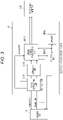
Fig. 3 is a diagram illustrating an internal configuration example of ascope connector circuit 401 included in ascope connector 400. -
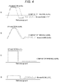
Fig. 4 is a diagram illustrating an example of a signal handled by thescope connector circuit 401.Fig. 4A illustrates an example of an output signal (MIPI D-PHY signal: video signal) of animaging unit 103.Fig. 4B illustrates an example of a signal (before separation) that is transmitted through a signal cable and input to thescope connector circuit 401.Fig. 4C illustrates an example of a signal (LP mode signal) after separation.Fig. 4D illustrates an example of a signal (HS mode signal) after separation and equalizer processing. -
Fig. 5 is a diagram illustrating an internal configuration example 1 of asignal separation unit 4011. -
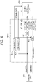
Fig. 6 is a diagram illustrating an internal configuration example 2 of thesignal separation unit 4011. -
Fig. 7 is a diagram illustrating an internal configuration example 3 of thesignal separation unit 4011. -
Fig. 8 is a diagram illustrating an internal configuration example 4 of thesignal separation unit 4011. -
Fig. 9 is a diagram illustrating detailed configurations oftransistors signal separation unit 4011. - Hereinafter, embodiments of the present disclosure will be described with reference to the drawings. In the following, an endoscope system will be described as an embodiment of the present disclosure.
- An observation target site in the endoscope system is, for example, respiratory organs or digestive organs. Examples of the respiratory organs include the lungs, the bronchus, the ears, the nose, and the throat. Examples of the digestive organs include the large intestine, the small intestine, the stomach, the esophagus, the duodenum, the uterus, and the bladder. In a case of observing the target sites as described above, it is more effective to utilize an image in which a specific biological structure is emphasized.
-
Fig. 1 is a diagram illustrating an example of an overall appearance of an endoscope system of the present embodiment, andFig. 2 is a diagram illustrating a schematic internal configuration example of the endoscope system of the present embodiment. Anendoscope system 1 includes an endoscope device (electronic scope) 100, aprocessor 200, and amonitor 300. Note that a scope connector (which may hereinafter be simply referred to as a "connector") 400 including a connector circuit according to a feature of the present embodiment is provided at a processor-side end portion of theendoscope device 100. - The
endoscope device 100 includes an elongatedtubular insertion portion 11 configured to be inserted into a subject. Theendoscope device 100 includes a light carrying bundle (LCB) 101 for guiding irradiation light from alight source device 201 to be described later, alight distribution lens 102 provided at an emission end of theLCB 101, animaging unit 103 that receives return light from an irradiated portion (observation site) via an objective lens (not illustrated), a driver signal processing circuit 105 that drives theimaging unit 103, and a first memory 106. - The irradiation light from the
light source device 201 enters the LCB 101 and propagates by repeating total reflection in the LCB 101. The irradiation light propagating in theLCB 101 is emitted from the emission end of theLCB 101 disposed in adistal end portion 12 of theinsertion portion 11, and irradiates the observation site through thelight distribution lens 102. The return light from the irradiated portion forms an optical image by each pixel on a light receiving surface of theimaging unit 103 via the objective lens. - The
imaging unit 103 is disposed in thedistal end portion 12 of theinsertion portion 11 and is, for example, a charge coupled device (CCD) image sensor. Theimaging unit 103 accumulates an optical image (return light from a living tissue) formed by each pixel on the light receiving surface, as charges corresponding to the amount of light, and generates and outputs image signals of R, G, and B. Note that theimaging unit 103 is not limited to a CCD image sensor, and may be replaced with a Complementary Metal Oxide Semiconductor (CMOS) image sensor or other types of imaging devices. A signal output from theimaging unit 103 is processed by ascope connector circuit 401 provided in thescope connector 400 as described later. - The
processor 200 is a device that integrally includes a signal processing device that processes a signal from theendoscope device 100 and a light source device that irradiates, via theendoscope device 100, a body cavity having difficulty in receiving natural light. In another embodiment, the signal processing device and the light source device may be provided separately. Theprocessor 200 includes thelight source device 201, asystem controller 202, anoptical filter 203, anoptical filter driver 204, a pre-stagesignal processing circuit 205, acolor conversion circuit 206, a post-stagesignal processing circuit 207, and a second memory 208. - The
processor 200 may include an operation panel (not illustrated). The operation panel may have various configurations. Examples of a specific configuration of the operation panel include a hardware key for each function mounted on a front surface of theprocessor 200, a touch panel type graphical user interface (GUI), a combination of a hardware key and a GUI, and the like. An operator can perform a mode switching operation described later with the operation panel. - The
system controller 202 executes various programs stored in a memory (not illustrated) and integrally controls theentire endoscope system 1. Thesystem controller 202 controls the operations and timings of various circuits in theprocessor 200 by using a control signal so as to perform processing suitable for theendoscope device 100 connected to theprocessor 200. Further, thesystem controller 202 may be connected to the above-described operation panel. Thesystem controller 202 changes each operation of theendoscope system 1 and a parameter for each operation in accordance with an operator's instruction input to the operation panel. - As the
light source device 201, for example, a high-brightness lamp such as a xenon lamp, a halogen lamp, a mercury lamp, or a metal halide lamp, or a light emitting diode (LED) can be used. The irradiation light from thelight source device 201 is light having a spectrum mainly spreading from a visible light range to an invisible infrared range (or light including at least the visible light range). The irradiation light from thelight source device 201 is incident on theoptical filter 203. - Data communication between the
endoscope device 100 and theprocessor 200 may use a wired electric communication scheme or an optical wireless communication scheme. - As illustrated in
Fig. 2 , theendoscope device 100 and theprocessor 200 are connected via thescope connector 400. Theconnector 400 includes an LCB constituting a part of theLCB 101 continuing from theprocessor 200 to theendoscope device 100, and thescope connector circuit 401. Thescope connector circuit 401 separates a low power (LP) mode signal and a high speed (HS) mode signal included in a MIPI D-PHY signal (video signal) output from theimaging unit 103, corrects (amplification by an equalizer and sensor-specific noise correction) the video signal attenuated by cable transmission in theendoscope device 100, multiplexes again the LP mode signal and the corrected HS mode signal, and supplies the multiplexed signal to theprocessor 200, which will be described in detail later. Further, thescope connector circuit 401 is provided in thescope connector 400 in the present embodiment, but is not necessarily provided in thescope connector 400. For example, a circuit corresponding to thescope connector circuit 401 may be provided in a connector unit on theprocessor 200 side or inside theprocessor 200. -
Fig. 3 is a diagram illustrating an internal configuration example of thescope connector circuit 401 included in thescope connector 400.Fig. 4 is a diagram illustrating an example of a signal handled by thescope connector circuit 401.Fig. 4A illustrates an example of an output signal (MIPI D-PHY signal: video signal) of theimaging unit 103.Fig. 4B illustrates an example of a signal (before separation) that is transmitted through a signal cable and input to thescope connector circuit 401.Fig. 4C illustrates an example of a signal (LP mode signal) after separation.Fig. 4D illustrates an example of a signal (HS mode signal) after separation and equalizer processing. - The
scope connector circuit 401 includes asignal separation unit 4011 that separates the MIPI D-PHY signal output from theimaging unit 103 and transmitted through the signal cable into the LP mode signal and the HS mode signal, anequalizer unit 4012 that amplifies the HS mode signal obtained by the separation to correct a distorted gain, a driversignal processing unit 4013 that is implemented by, for example, an FPGA and corrects noise (point damage) unique to theimaging unit 103 or multiplexes the LP mode signal and the corrected HS mode signal and outputs the multiplexed signal to theprocessor 200, acontrol unit 4014 that performs register setting or the like (for example, setting for changing a shutter speed and a gain according to brightness and darkness in the body into which the scope is inserted) of theimaging unit 103, and amemory 4015 that stores an initial setting value of theimaging unit 103, configuration data of the driversignal processing unit 4013, and the like. Note that the number of video lanes (the number of chs) from theimaging unit 103 is determined by the resolution of the image sensor. Further, the driversignal processing unit 4013 may be caused to perform the processing performed by thecontrol unit 4014. - The signal (MIPI D-PHY signal) output from the
imaging unit 103 is, for example, a signal in a form in which the high speed mode (HS mode) signal is transmitted after the low power mode (LP mode) signal is transmitted. As illustrated inFig. 4A , the low power mode (LP mode) signal has a higher larger level (voltage amplitude) and a lower transmission rate than the high speed mode (HS mode) signal. Since the transmission rate is low, it can be said that degradation of the signal level of the low power mode (LP mode) signal due to cable transmission is less likely to occur than the high speed mode (HS mode) signal. - In a case where the MIPI D-PHY signal is transmitted through the signal cable of the endoscope device 100 (over a distance longer than a distance recommended by the MIPI D-PHY standard), the low power mode (LP mode) signal and the high speed mode (HS mode) signal are distorted as illustrated in
Fig. 4B . The signal level of the low power mode (LP mode) signal is higher than a comparator threshold level (a threshold for distinguishing and extracting the LP mode signal) even if the signal is somewhat blurred, and thus it can be seen that the low power mode (LP mode) signal is hardly affected by cable transmission. On the other hand, since the signal level of the high speed mode (HS mode) signal itself is low, the signal is distorted by cable transmission, and it is difficult for the processor at the subsequent stage to perform signal processing as it is. Therefore, in the present embodiment, theequalizer unit 4012 amplifies the distorted high speed mode (HS mode) signal to perform level correction so as not to affect signal processing in the subsequent stage. - The low power mode (LP mode) signal obtained by being separated by the
signal separation unit 4011 can be extracted as a clean square wave as illustrated inFig. 4C by setting an appropriate comparator threshold level even if the signal is somewhat distorted by cable transmission (Fig. 4B ). - As illustrated in
Fig. 4D , the level of the high speed mode (HS mode) signal separated by thesignal separation unit 4011 and corrected by theequalizer unit 4012 is corrected to implement a clear differential signal like the HS mode signal portion of the MIPI D-PHY signal (Fig. 4A ) before separation. -
Figs. 5 to 9 are diagrams related to an internal configuration example of thesignal separation unit 4011. - The
signal separation unit 4011 according to the internal configuration example illustrated inFig. 5 includes a plurality ofLP resistors comparators HS resistors equalizer 506 that is connected in parallel with the video chs between theHS resistors - Resistance values of the
LP resistors HS resistors HS resistors equalizer 506 and the impedance on an output side (an input side of the driver signal processing unit (for example, FPGA) 4013) can be matched by arranging theHS resistors - The comparator threshold of the
comparators Fig. 4C is supplied to the driversignal processing unit 4013. - The
signal separation unit 4011 according to the internal configuration example illustrated inFig. 6 includes a plurality ofcomparators switches comparators HS resistors switches equalizer 506 that is connected in parallel with the video chs between theHS resistors - The
switches Fig. 4C after the extraction of the LP mode signal is completed by thecomparators switches Fig. 4B ) is supplied to the equalizer, and attenuation is corrected (amplified). - Note that the comparator threshold and the
HS resistors - The
signal separation unit 4011 according to the internal configuration example illustrated inFig. 7 includes a plurality of LP mode switches (SW_LPs) 701 and 702 connected in series with video chs (DataO-Pch, DataO-Nch, ..., DataN-Pch, and DataN-Nch), a plurality ofcomparators HS resistors SW_HSs equalizer 506 that is connected in parallel with the video chs between theHS resistors - The driver signal processing unit 4013 (or a control unit (not illustrated) such as a separately provided central processing unit (CPU)) controls the
SW LPs SW_HSs imaging unit 103. Then, the driversignal processing unit 4013 acquires an appearance timing (appearance position) of the LP mode signal from the video signals acquired in the initial operation period. Since the period of one cycle of the video signal (MIPI D-PHY signal) is known in advance, in an operation period after the initial operation period, the driversignal processing unit 4013 controls theSW_LPs SW HSs SW LPs SW HSs - The LP mode signal of the LP mode path acquired by the switching operation is shaped by the
comparators signal processing unit 4013. On the other hand, the attenuation of the HS mode signal of the HS mode path acquired by the switching operation is corrected by theequalizer 506 and supplied to the driversignal processing unit 4013. - Note that the comparator threshold and the
HS resistors - The
signal separation unit 4011 according to the internal configuration example illustrated inFig. 8 includestransistors 801 and 802 (transistors are used instead of the LP mode switches (SW_LPs) 701 and 702 of the configuration example 3 (Fig. 7 )) connected in series with video chs (DataO-Pch, DataO-Nch, ..., DataN-Pch, and DataN-Nch), field effect transistors (FETs) 803 and 804 (FETs are used instead of thecomparators 503 and 504) connected in series with thetransistors HS resistors SW HSs equalizer 506 that is connected in parallel with the video chs between theHS resistors - The driver signal processing unit 4013 (or a control unit (not illustrated) such as a separately provided CPU) controls the
SW_HSs imaging unit 103. Then, the driversignal processing unit 4013 acquires an appearance timing (appearance position) of the LP mode signal from the video signals acquired in the initial operation period. Since the period of one cycle of the video signal (MIPI D-PHY signal) is known in advance, in an operation period after the initial operation period, the driversignal processing unit 4013 controls theSW_HSs 85 and 806 to be turned off in a period in which the LP mode signal arrives, and controls theSW_HSs - The LP mode signal of the LP mode path acquired by the switching operation is shaped by the
FETs signal processing unit 4013. On the other hand, the attenuation of the HS mode signal of the HS mode path acquired by the switching operation is corrected by theequalizer 506 and supplied to the driversignal processing unit 4013. - Note that the comparator threshold and the
HS resistors -
Fig. 9 is a diagram illustrating detailed configurations of thetransistors FETs transistors FETs - According to the present embodiment, the
scope connector circuit 401 is provided in thescope connector 400 of theendoscope device 100, and a video signal (a signal based on the MIPI D-PHY standard) from the imaging unit (image sensor) 103 is subjected to signal processing. Specifically, the scope connector circuit (attenuation correction unit) 401 separates the LP mode signal and the HS mode signal included in the MIPI D-PHY signal, corrects the attenuation of the HS mode signal (attenuation caused by cable transmission), multiplexes the separated LP mode signal and the HS mode signal subjected to the attenuation correction (returning to a signal format according to the MIPI D-PHY standard), and outputs the multiplexed signal to theprocessor 200. By doing so, theprocessor 200 can process the signal based on the MIPI D-PHY standard as it is without converting the signal into another format. - Furthermore, in the present embodiment, since the attenuation correction unit is provided in the
scope connector 400 at a place other than the insertion portion of the endoscope device (scope) 100 and the endoscope operation unit (the attenuation correction unit is provided in thescope connector 400 in the embodiment, but the attenuation correction unit may be provided in other places, for example, a connector unit on the processor side or inside the processor 200), there is no need to increase the size of the insertion portion and the operation unit of the endoscope device. - An endoscope system including:
- an endoscope device that includes an endoscope-side connector unit;
- a processor that includes a processor-side connector unit; and
- an attenuation correction unit that corrects attenuation of a video signal from an image sensor disposed at a distal end portion of the endoscope device.
- The endoscope system according to Specified
Matter 1, in which the attenuation correction unit is provided in the endoscope-side connector unit. - The endoscope system according to Specified
Matter 1 or 2, in which the video signal from the image sensor includes a signal conforming to an MIPI D-PHY standard, and
the attenuation correction unit includes: - a separation unit that separates the video signal into a low power mode signal and a high speed mode signal;
- an equalizer unit that corrects attenuation of the high speed mode signal; and
- a driver signal processing unit that multiplexes the low power mode signal extracted from the video signal and the high speed mode signal subjected to the attenuation correction and outputs the multiplexed signal to the processor.
- The endoscope system according to Specified Matter 3, in which the processor processes the video signal as a signal based on the MIPI D-PHY standard.
- The endoscope system according to Specified Matter 3 or 4, in which the separation unit includes a first path for processing the low power mode signal and a second path for processing the high speed mode signal,
- a first type resistor and a comparator are provided in the first path, the first type resistor being connected in series with a signal line of the image sensor, the comparator being connected in series with the first type resistor and extracting a signal whose level is equal to or higher than a predetermined threshold level from signals passing through the first type resistor, and
- an equalizer that is connected in parallel with the signal line of the image sensor is provided in the second path.
- The endoscope system according to Specified Matter 3 or 4, in which the separation unit includes a first path for processing the low power mode signal and a second path for processing the high speed mode signal,
- a comparator that is connected in series with a signal line of the image sensor and extracts a signal whose level is equal to or higher than a predetermined threshold level from the video signal is provided in the first path, and
- a switch and an equalizer are provided in the second path, the switch being connected in series with the signal line of the image sensor and being closed at a timing of extraction of the low power mode signal from the comparator, the equalizer being connected in parallel with the signal line of the image sensor.
- The endoscope system according to Specified Matter 3 or 4, in which the separation unit includes a first path for processing the low power mode signal and a second path for processing the high speed mode signal,
- a first type switch and a comparator are provided in the first path, the first type switch being connected in series with a signal line of the image sensor, the comparator being connected in series with the signal line of the image sensor and extracting a signal whose level is equal to or higher than a predetermined threshold level from the video signal,
- a second type switch and an equalizer are provided in the second path, the second type switch being connected in series with the signal line of the image sensor, the equalizer being connected in parallel with the signal line of the image sensor, and
- the driver signal processing unit controls the first type switch to be turned on and controls the second type switch to be turned off so as to recognize, from the video signal input from the image sensor, a period of the low power mode signal and a period of the high speed mode signal, and, after recognizing the periods, the driver signal processing unit controls the first type switch to be turned on and controls the second type switch to be turned off during the period of the low power mode signal, and controls the first type switch to be turned off and controls the second type switch to be turned on during the period of the high speed mode signal.
- The endoscope system according to Specified Matter 3 or 4, in which the separation unit includes a first path for processing the low power mode signal and a second path for processing the high speed mode signal,
- a transistor and a field effect transistor (FET) are provided in the first path, the transistor being connected in series with a signal line of the image sensor, the FET being connected in series with the signal line of the image sensor and extracting a signal whose level is equal to or higher than a predetermined threshold level from the video signal,
- a switch and an equalizer are provided in the second path, the switch being connected in series with the signal line of the image sensor, the equalizer being connected in parallel with the signal line of the image sensor, and
- the driver signal processing unit controls the switch to be turned off so as to recognize, from the video signal input from the image sensor, a period of the low power mode signal and a period of the high speed mode signal, and, after recognizing the periods, the driver signal processing unit controls the switch to be turned off during the period of the low power mode signal, and controls the switch to be turned on during the period of the high speed mode signal.
-
- 1
- Endoscope system
- 100
- Endoscope device
- 110
- Connector unit of endoscope device
- 200
- Processor
- 210
- Connector unit of processor
- 300
- Monitor
- 400
- Scope connector
- 401
- Scope connector circuit
- 4011
- Signal separation unit
- 4012
- Equalizer unit
- 4013
- Driver signal processing unit
- 4014
- Control unit
- 4015
- Memory
Claims (8)
- An endoscope system comprising:an endoscope device that includes an endoscope-side connector unit;a processor that includes a processor-side connector unit; andan attenuation correction unit that corrects attenuation of a video signal from an image sensor disposed at a distal end portion of the endoscope device.
- The endoscope system according to claim 1, wherein
the attenuation correction unit is provided in the endoscope-side connector unit. - The endoscope system according to claim 1 or 2, whereinthe video signal from the image sensor includes a signal conforming to the MIPI D-PHY standard, andthe attenuation correction unit includes:a separation unit that separates the video signal into a low power mode signal and a high speed mode signal;an equalizer unit that corrects attenuation of the high speed mode signal; anda driver signal processing unit that multiplexes the low power mode signal extracted from the video signal and the high speed mode signal subjected to attenuation correction and outputs the multiplexed signal to the processor.
- The endoscope system according to claim 3, wherein
the processor processes the video signal as a signal based on the MIPI D-PHY standard. - The endoscope system according to claim 3 or 4, whereinthe separation unit includes a first path for processing the low power mode signal and a second path for processing the high speed mode signal,a first type resistor and a comparator are provided in the first path, the first type resistor being connected in series with a signal line of the image sensor, the comparator being connected in series with the first type resistor and extracting a signal whose level is equal to or higher than a predetermined threshold level from signals passing through the first type resistor, andan equalizer that is connected in parallel with the signal line of the image sensor is provided in the second path.
- The endoscope system according to claim 3 or 4, whereinthe separation unit includes a first path for processing the low power mode signal and a second path for processing the high speed mode signal,a comparator that is connected in series with a signal line of the image sensor and extracts a signal whose level is equal to or higher than a predetermined threshold level from the video signal is provided in the first path, anda switch and an equalizer are provided in the second path, the switch being connected in series with the signal line of the image sensor and being closed at a timing of extraction of the low power mode signal from the comparator, the equalizer being connected in parallel with the signal line of the image sensor.
- The endoscope system according to claim 3 or 4, whereinthe separation unit includes a first path for processing the low power mode signal and a second path for processing the high speed mode signal,a first type switch and a comparator are provided in the first path, the first type switch being connected in series with a signal line of the image sensor, the comparator being connected in series with the signal line of the image sensor and extracting a signal whose level is equal to or higher than a predetermined threshold level from the video signal,a second type switch and an equalizer are provided in the second path, the second type switch being connected in series with the signal line of the image sensor, the equalizer being connected in parallel with the signal line of the image sensor, andthe driver signal processing unit controls the first type switch to be turned on and controls the second type switch to be turned off so as to recognize, from the video signal input from the image sensor, a period of the low power mode signal and a period of the high speed mode signal, and, after recognizing the periods, the driver signal processing unit controls the first type switch to be turned on and controls the second type switch to be turned off during the period of the low power mode signal, and controls the first type switch to be turned off and controls the second type switch to be turned on during the period of the high speed mode signal.
- The endoscope system according to claim 3 or 4, whereinthe separation unit includes a first path for processing the low power mode signal and a second path for processing the high speed mode signal,a transistor and a field effect transistor (FET) are provided in the first path, the transistor being connected in series with a signal line of the image sensor, the FET being connected in series with the signal line of the image sensor and extracting a signal whose level is equal to or higher than a predetermined threshold level from the video signal,a switch and an equalizer are provided in the second path, the switch being connected in series with the signal line of the image sensor, the equalizer being connected in parallel with the signal line of the image sensor, andthe driver signal processing unit controls the switch to be turned off so as to recognize, from the video signal input from the image sensor, a period of the low power mode signal and a period of the high speed mode signal, and, after recognizing the periods, the driver signal processing unit controls the switch to be turned off during the period of the low power mode signal, and controls the switch to be turned on during the period of the high speed mode signal.
Applications Claiming Priority (2)
| Application Number | Priority Date | Filing Date | Title |
|---|---|---|---|
| JP2020035625A JP7536472B2 (en) | 2020-03-03 | 2020-03-03 | Endoscope System |
| PCT/JP2021/007247 WO2021177148A1 (en) | 2020-03-03 | 2021-02-26 | Endoscope system |
Publications (3)
| Publication Number | Publication Date |
|---|---|
| EP4115790A1 true EP4115790A1 (en) | 2023-01-11 |
| EP4115790A4 EP4115790A4 (en) | 2024-04-10 |
| EP4115790B1 EP4115790B1 (en) | 2026-04-15 |
Family
ID=77614286
Family Applications (1)
| Application Number | Title | Priority Date | Filing Date |
|---|---|---|---|
| EP21763646.3A Active EP4115790B1 (en) | 2020-03-03 | 2021-02-26 | Endoscope system |
Country Status (5)
| Country | Link |
|---|---|
| US (1) | US12016521B2 (en) |
| EP (1) | EP4115790B1 (en) |
| JP (1) | JP7536472B2 (en) |
| CN (1) | CN115279248A (en) |
| WO (1) | WO2021177148A1 (en) |
Families Citing this family (1)
| Publication number | Priority date | Publication date | Assignee | Title |
|---|---|---|---|---|
| CN117215982B (en) * | 2023-09-06 | 2024-11-29 | 北京科加触控技术有限公司 | MIPI signal transmission distance extension module for optical touch devices |
Family Cites Families (31)
| Publication number | Priority date | Publication date | Assignee | Title |
|---|---|---|---|---|
| JP3262893B2 (en) * | 1993-05-20 | 2002-03-04 | オリンパス光学工業株式会社 | Endoscope image display device |
| EP2064629B1 (en) * | 2006-09-18 | 2010-02-24 | Nxp B.V. | Improved mode switching of a data communications link |
| JP2008264252A (en) * | 2007-04-20 | 2008-11-06 | Olympus Medical Systems Corp | Electronic endoscope device |
| DE102010027400B4 (en) * | 2010-07-15 | 2020-06-25 | Karl Storz Se & Co. Kg | Endoscopic instrument and use of a star quad |
| JP2012115531A (en) * | 2010-12-02 | 2012-06-21 | Hoya Corp | Electronic endoscope and electronic endoscope system |
| US20120310045A1 (en) * | 2011-06-06 | 2012-12-06 | Fujikura Ltd. | Electronic endoscope |
| DE102011106386A1 (en) * | 2011-07-04 | 2013-01-10 | Karl Storz Gmbh & Co. Kg | Endoscopic arrangement |
| US9020418B2 (en) | 2012-02-29 | 2015-04-28 | Fairchild Semiconductor Corporation | Methods and apparatus related to a repeater |
| JP6005989B2 (en) * | 2012-05-16 | 2016-10-12 | オリンパス株式会社 | Endoscope device |
| EP3103379A4 (en) * | 2014-05-08 | 2017-11-22 | Olympus Corporation | Electronic endoscope |
| WO2016035829A1 (en) * | 2014-09-05 | 2016-03-10 | オリンパス株式会社 | Imaging device and processing device |
| JP5861071B1 (en) | 2014-10-14 | 2016-02-16 | パナソニックIpマネジメント株式会社 | Endoscope |
| WO2016088421A1 (en) * | 2014-12-04 | 2016-06-09 | オリンパス株式会社 | Endoscope |
| US9491495B2 (en) * | 2015-01-16 | 2016-11-08 | Analog Devices Global | Method and apparatus for providing input to a camera serial interface transmitter |
| KR102186742B1 (en) * | 2015-06-25 | 2020-12-04 | 인더스마트 주식회사 | Multi image processing apparatus and multi image processing method of android system for high speed and short distance interface |
| JPWO2017104190A1 (en) | 2015-12-14 | 2018-10-04 | オリンパス株式会社 | Endoscope system |
| US10078211B2 (en) * | 2015-12-29 | 2018-09-18 | INTHESMART Inc. | Apparatus for transferring image data and endoscopy system including the same |
| JPWO2017122586A1 (en) | 2016-01-12 | 2018-11-01 | オリンパス株式会社 | Endoscope device |
| CN109310281B (en) * | 2016-08-02 | 2021-03-12 | 奥林巴斯株式会社 | Endoscope system and signal processing device |
| JP6360988B1 (en) * | 2016-09-05 | 2018-07-18 | オリンパス株式会社 | Endoscope and endoscope system |
| CN110089108B (en) * | 2016-12-21 | 2021-07-09 | 奥林巴斯株式会社 | Imaging element, imaging device, and endoscope |
| KR102293580B1 (en) * | 2017-06-08 | 2021-08-26 | 현대모비스 주식회사 | Curtain airbag apparatus |
| KR102171940B1 (en) * | 2018-08-24 | 2020-11-02 | 인더스마트 주식회사 | Endoscope apparatus |
| JP6608022B2 (en) * | 2018-10-02 | 2019-11-20 | パナソニック株式会社 | Endoscope |
| WO2020144755A1 (en) * | 2019-01-09 | 2020-07-16 | オリンパス株式会社 | Imaging system |
| JP7272632B2 (en) * | 2019-03-14 | 2023-05-12 | i-PRO株式会社 | Endoscope |
| US11023409B2 (en) * | 2019-10-03 | 2021-06-01 | Qualcomm Incorporated | MIPI D-PHY receiver auto rate detection and high-speed settle time control |
| US10902572B1 (en) * | 2019-10-09 | 2021-01-26 | Karl Storz Imaging, Inc. | Enhanced fluorescence imaging for imaging system |
| WO2021124546A1 (en) * | 2019-12-20 | 2021-06-24 | オリンパス株式会社 | Endoscope system |
| DE102021134433B4 (en) * | 2021-12-22 | 2024-05-02 | Karl Storz Se & Co. Kg | Medical observation device |
| US12032509B2 (en) * | 2022-03-31 | 2024-07-09 | e-con Systems India Private Limited | System and method for camera serial interface lane implementation between camera sensor and host processor |
-
2020
- 2020-03-03 JP JP2020035625A patent/JP7536472B2/en active Active
-
2021
- 2021-02-26 US US17/799,174 patent/US12016521B2/en active Active
- 2021-02-26 CN CN202180018620.6A patent/CN115279248A/en active Pending
- 2021-02-26 EP EP21763646.3A patent/EP4115790B1/en active Active
- 2021-02-26 WO PCT/JP2021/007247 patent/WO2021177148A1/en not_active Ceased
Also Published As
| Publication number | Publication date |
|---|---|
| EP4115790A4 (en) | 2024-04-10 |
| US20230102158A1 (en) | 2023-03-30 |
| JP7536472B2 (en) | 2024-08-20 |
| WO2021177148A1 (en) | 2021-09-10 |
| JP2021137150A (en) | 2021-09-16 |
| EP4115790B1 (en) | 2026-04-15 |
| US12016521B2 (en) | 2024-06-25 |
| CN115279248A (en) | 2022-11-01 |
Similar Documents
| Publication | Publication Date | Title |
|---|---|---|
| US9826891B2 (en) | Endoscope apparatus and image pickup control method thereof | |
| US8749625B2 (en) | Method for resetting CMOS imaging element in endoscope apparatus | |
| US20130300849A1 (en) | Imaging apparatus | |
| EP2689718A1 (en) | Imaging system | |
| CN105934942B (en) | Photographic device and processing unit | |
| CN112788978A (en) | Processor for endoscope, information processing device, endoscope system, program, and information processing method | |
| WO2014002732A1 (en) | Imaging device and imaging system | |
| EP2735261B1 (en) | Imaging system | |
| US20140171738A1 (en) | Endoscope apparatus and image pickup control method thereof | |
| CN107072506B (en) | Camera and Processing Unit | |
| US20170172387A1 (en) | Endoscope system | |
| US12016521B2 (en) | Endoscope system | |
| CN113271838A (en) | Endoscope system and image processing apparatus | |
| JP5926980B2 (en) | Imaging apparatus and imaging system | |
| JPWO2015198659A1 (en) | Imaging apparatus and endoscope apparatus | |
| US9526404B2 (en) | Endoscope illumination system | |
| JP6489644B2 (en) | Imaging system | |
| US8723921B2 (en) | Image pickup system | |
| JP5336410B2 (en) | Endoscope system and operating method thereof | |
| US11297257B2 (en) | Image pickup system | |
| JP5885617B2 (en) | Imaging system | |
| JP2011235021A (en) | Electronic endoscope system | |
| JP5826977B1 (en) | Imaging device, endoscope, endoscope system, and driving method of imaging device | |
| US20160323531A1 (en) | Transmission system and processing device | |
| WO2016006302A1 (en) | Imaging element, imaging device, endoscope, endoscope system, and method for driving imaging element |
Legal Events
| Date | Code | Title | Description |
|---|---|---|---|
| STAA | Information on the status of an ep patent application or granted ep patent |
Free format text: STATUS: THE INTERNATIONAL PUBLICATION HAS BEEN MADE |
|
| PUAI | Public reference made under article 153(3) epc to a published international application that has entered the european phase |
Free format text: ORIGINAL CODE: 0009012 |
|
| STAA | Information on the status of an ep patent application or granted ep patent |
Free format text: STATUS: REQUEST FOR EXAMINATION WAS MADE |
|
| 17P | Request for examination filed |
Effective date: 20220922 |
|
| AK | Designated contracting states |
Kind code of ref document: A1 Designated state(s): AL AT BE BG CH CY CZ DE DK EE ES FI FR GB GR HR HU IE IS IT LI LT LU LV MC MK MT NL NO PL PT RO RS SE SI SK SM TR |
|
| DAV | Request for validation of the european patent (deleted) | ||
| DAX | Request for extension of the european patent (deleted) | ||
| A4 | Supplementary search report drawn up and despatched |
Effective date: 20240307 |
|
| RIC1 | Information provided on ipc code assigned before grant |
Ipc: A61B 1/05 20060101ALI20240301BHEP Ipc: H04L 25/03 20060101ALI20240301BHEP Ipc: H04L 25/02 20060101ALI20240301BHEP Ipc: A61B 1/045 20060101ALI20240301BHEP Ipc: A61B 1/00 20060101AFI20240301BHEP |
|
| GRAP | Despatch of communication of intention to grant a patent |
Free format text: ORIGINAL CODE: EPIDOSNIGR1 |
|
| STAA | Information on the status of an ep patent application or granted ep patent |
Free format text: STATUS: GRANT OF PATENT IS INTENDED |
|
| RIC1 | Information provided on ipc code assigned before grant |
Ipc: A61B 1/00 20060101AFI20251205BHEP Ipc: A61B 1/045 20060101ALI20251205BHEP Ipc: H04L 25/02 20060101ALI20251205BHEP Ipc: H04L 25/03 20060101ALI20251205BHEP Ipc: A61B 1/05 20060101ALI20251205BHEP |
|
| INTG | Intention to grant announced |
Effective date: 20251223 |
|
| GRAS | Grant fee paid |
Free format text: ORIGINAL CODE: EPIDOSNIGR3 |
|
| GRAA | (expected) grant |
Free format text: ORIGINAL CODE: 0009210 |
|
| STAA | Information on the status of an ep patent application or granted ep patent |
Free format text: STATUS: THE PATENT HAS BEEN GRANTED |
|
| AK | Designated contracting states |
Kind code of ref document: B1 Designated state(s): AL AT BE BG CH CY CZ DE DK EE ES FI FR GB GR HR HU IE IS IT LI LT LU LV MC MK MT NL NO PL PT RO RS SE SI SK SM TR |
|
| REG | Reference to a national code |
Ref country code: CH Ref legal event code: F10 Free format text: ST27 STATUS EVENT CODE: U-0-0-F10-F00 (AS PROVIDED BY THE NATIONAL OFFICE) Effective date: 20260415 |
|
| REG | Reference to a national code |
Ref country code: DE Ref legal event code: R096 Ref document number: 602021052139 Country of ref document: DE |