EP4113819B1 - Switching conversion circuit and control method - Google Patents
Switching conversion circuit and control method Download PDFInfo
- Publication number
- EP4113819B1 EP4113819B1 EP22181881.8A EP22181881A EP4113819B1 EP 4113819 B1 EP4113819 B1 EP 4113819B1 EP 22181881 A EP22181881 A EP 22181881A EP 4113819 B1 EP4113819 B1 EP 4113819B1
- Authority
- EP
- European Patent Office
- Prior art keywords
- value
- voltage
- switching
- switching transistor
- controller
- Prior art date
- Legal status (The legal status is an assumption and is not a legal conclusion. Google has not performed a legal analysis and makes no representation as to the accuracy of the status listed.)
- Active
Links
Images



Classifications
-
- H—ELECTRICITY
- H02—GENERATION; CONVERSION OR DISTRIBUTION OF ELECTRIC POWER
- H02M—APPARATUS FOR CONVERSION BETWEEN AC AND AC, BETWEEN AC AND DC, OR BETWEEN DC AND DC, AND FOR USE WITH MAINS OR SIMILAR POWER SUPPLY SYSTEMS; CONVERSION OF DC OR AC INPUT POWER INTO SURGE OUTPUT POWER; CONTROL OR REGULATION THEREOF
- H02M1/00—Details of apparatus for conversion
- H02M1/0003—Details of control, feedback or regulation circuits
- H02M1/0006—Arrangements for supplying an adequate voltage to the control circuit of converters
-
- H—ELECTRICITY
- H02—GENERATION; CONVERSION OR DISTRIBUTION OF ELECTRIC POWER
- H02M—APPARATUS FOR CONVERSION BETWEEN AC AND AC, BETWEEN AC AND DC, OR BETWEEN DC AND DC, AND FOR USE WITH MAINS OR SIMILAR POWER SUPPLY SYSTEMS; CONVERSION OF DC OR AC INPUT POWER INTO SURGE OUTPUT POWER; CONTROL OR REGULATION THEREOF
- H02M1/00—Details of apparatus for conversion
- H02M1/0048—Circuits or arrangements for reducing losses
- H02M1/0054—Transistor switching losses
- H02M1/0058—Transistor switching losses by employing soft switching techniques, i.e. commutation of transistors when applied voltage is zero or when current flow is zero
-
- H—ELECTRICITY
- H02—GENERATION; CONVERSION OR DISTRIBUTION OF ELECTRIC POWER
- H02M—APPARATUS FOR CONVERSION BETWEEN AC AND AC, BETWEEN AC AND DC, OR BETWEEN DC AND DC, AND FOR USE WITH MAINS OR SIMILAR POWER SUPPLY SYSTEMS; CONVERSION OF DC OR AC INPUT POWER INTO SURGE OUTPUT POWER; CONTROL OR REGULATION THEREOF
- H02M1/00—Details of apparatus for conversion
- H02M1/08—Circuits specially adapted for the generation of control voltages for semiconductor devices incorporated in static converters
- H02M1/083—Circuits specially adapted for the generation of control voltages for semiconductor devices incorporated in static converters for the ignition at the zero crossing of the voltage or the current
-
- H—ELECTRICITY
- H02—GENERATION; CONVERSION OR DISTRIBUTION OF ELECTRIC POWER
- H02M—APPARATUS FOR CONVERSION BETWEEN AC AND AC, BETWEEN AC AND DC, OR BETWEEN DC AND DC, AND FOR USE WITH MAINS OR SIMILAR POWER SUPPLY SYSTEMS; CONVERSION OF DC OR AC INPUT POWER INTO SURGE OUTPUT POWER; CONTROL OR REGULATION THEREOF
- H02M1/00—Details of apparatus for conversion
- H02M1/32—Means for protecting converters other than automatic disconnection
-
- H—ELECTRICITY
- H02—GENERATION; CONVERSION OR DISTRIBUTION OF ELECTRIC POWER
- H02M—APPARATUS FOR CONVERSION BETWEEN AC AND AC, BETWEEN AC AND DC, OR BETWEEN DC AND DC, AND FOR USE WITH MAINS OR SIMILAR POWER SUPPLY SYSTEMS; CONVERSION OF DC OR AC INPUT POWER INTO SURGE OUTPUT POWER; CONTROL OR REGULATION THEREOF
- H02M1/00—Details of apparatus for conversion
- H02M1/36—Means for starting or stopping converters
-
- H—ELECTRICITY
- H02—GENERATION; CONVERSION OR DISTRIBUTION OF ELECTRIC POWER
- H02M—APPARATUS FOR CONVERSION BETWEEN AC AND AC, BETWEEN AC AND DC, OR BETWEEN DC AND DC, AND FOR USE WITH MAINS OR SIMILAR POWER SUPPLY SYSTEMS; CONVERSION OF DC OR AC INPUT POWER INTO SURGE OUTPUT POWER; CONTROL OR REGULATION THEREOF
- H02M3/00—Conversion of DC power input into DC power output
- H02M3/01—Resonant DC/DC converters
-
- H—ELECTRICITY
- H02—GENERATION; CONVERSION OR DISTRIBUTION OF ELECTRIC POWER
- H02M—APPARATUS FOR CONVERSION BETWEEN AC AND AC, BETWEEN AC AND DC, OR BETWEEN DC AND DC, AND FOR USE WITH MAINS OR SIMILAR POWER SUPPLY SYSTEMS; CONVERSION OF DC OR AC INPUT POWER INTO SURGE OUTPUT POWER; CONTROL OR REGULATION THEREOF
- H02M3/00—Conversion of DC power input into DC power output
- H02M3/22—Conversion of DC power input into DC power output with intermediate conversion into AC
- H02M3/24—Conversion of DC power input into DC power output with intermediate conversion into AC by static converters
- H02M3/28—Conversion of DC power input into DC power output with intermediate conversion into AC by static converters using discharge tubes with control electrode or semiconductor devices with control electrode to produce the intermediate AC
- H02M3/325—Conversion of DC power input into DC power output with intermediate conversion into AC by static converters using discharge tubes with control electrode or semiconductor devices with control electrode to produce the intermediate AC using devices of a triode or a transistor type requiring continuous application of a control signal
- H02M3/335—Conversion of DC power input into DC power output with intermediate conversion into AC by static converters using discharge tubes with control electrode or semiconductor devices with control electrode to produce the intermediate AC using devices of a triode or a transistor type requiring continuous application of a control signal using semiconductor devices only
- H02M3/33569—Conversion of DC power input into DC power output with intermediate conversion into AC by static converters using discharge tubes with control electrode or semiconductor devices with control electrode to produce the intermediate AC using devices of a triode or a transistor type requiring continuous application of a control signal using semiconductor devices only having several active switching elements
-
- H—ELECTRICITY
- H02—GENERATION; CONVERSION OR DISTRIBUTION OF ELECTRIC POWER
- H02M—APPARATUS FOR CONVERSION BETWEEN AC AND AC, BETWEEN AC AND DC, OR BETWEEN DC AND DC, AND FOR USE WITH MAINS OR SIMILAR POWER SUPPLY SYSTEMS; CONVERSION OF DC OR AC INPUT POWER INTO SURGE OUTPUT POWER; CONTROL OR REGULATION THEREOF
- H02M3/00—Conversion of DC power input into DC power output
- H02M3/22—Conversion of DC power input into DC power output with intermediate conversion into AC
- H02M3/24—Conversion of DC power input into DC power output with intermediate conversion into AC by static converters
- H02M3/28—Conversion of DC power input into DC power output with intermediate conversion into AC by static converters using discharge tubes with control electrode or semiconductor devices with control electrode to produce the intermediate AC
- H02M3/325—Conversion of DC power input into DC power output with intermediate conversion into AC by static converters using discharge tubes with control electrode or semiconductor devices with control electrode to produce the intermediate AC using devices of a triode or a transistor type requiring continuous application of a control signal
- H02M3/335—Conversion of DC power input into DC power output with intermediate conversion into AC by static converters using discharge tubes with control electrode or semiconductor devices with control electrode to produce the intermediate AC using devices of a triode or a transistor type requiring continuous application of a control signal using semiconductor devices only
- H02M3/33569—Conversion of DC power input into DC power output with intermediate conversion into AC by static converters using discharge tubes with control electrode or semiconductor devices with control electrode to produce the intermediate AC using devices of a triode or a transistor type requiring continuous application of a control signal using semiconductor devices only having several active switching elements
- H02M3/33571—Half-bridge at primary side of an isolation transformer
-
- H—ELECTRICITY
- H02—GENERATION; CONVERSION OR DISTRIBUTION OF ELECTRIC POWER
- H02M—APPARATUS FOR CONVERSION BETWEEN AC AND AC, BETWEEN AC AND DC, OR BETWEEN DC AND DC, AND FOR USE WITH MAINS OR SIMILAR POWER SUPPLY SYSTEMS; CONVERSION OF DC OR AC INPUT POWER INTO SURGE OUTPUT POWER; CONTROL OR REGULATION THEREOF
- H02M3/00—Conversion of DC power input into DC power output
- H02M3/22—Conversion of DC power input into DC power output with intermediate conversion into AC
- H02M3/24—Conversion of DC power input into DC power output with intermediate conversion into AC by static converters
- H02M3/28—Conversion of DC power input into DC power output with intermediate conversion into AC by static converters using discharge tubes with control electrode or semiconductor devices with control electrode to produce the intermediate AC
- H02M3/325—Conversion of DC power input into DC power output with intermediate conversion into AC by static converters using discharge tubes with control electrode or semiconductor devices with control electrode to produce the intermediate AC using devices of a triode or a transistor type requiring continuous application of a control signal
- H02M3/335—Conversion of DC power input into DC power output with intermediate conversion into AC by static converters using discharge tubes with control electrode or semiconductor devices with control electrode to produce the intermediate AC using devices of a triode or a transistor type requiring continuous application of a control signal using semiconductor devices only
- H02M3/33569—Conversion of DC power input into DC power output with intermediate conversion into AC by static converters using discharge tubes with control electrode or semiconductor devices with control electrode to produce the intermediate AC using devices of a triode or a transistor type requiring continuous application of a control signal using semiconductor devices only having several active switching elements
- H02M3/33576—Conversion of DC power input into DC power output with intermediate conversion into AC by static converters using discharge tubes with control electrode or semiconductor devices with control electrode to produce the intermediate AC using devices of a triode or a transistor type requiring continuous application of a control signal using semiconductor devices only having several active switching elements having at least one active switching element at the secondary side of an isolation transformer
-
- H—ELECTRICITY
- H02—GENERATION; CONVERSION OR DISTRIBUTION OF ELECTRIC POWER
- H02M—APPARATUS FOR CONVERSION BETWEEN AC AND AC, BETWEEN AC AND DC, OR BETWEEN DC AND DC, AND FOR USE WITH MAINS OR SIMILAR POWER SUPPLY SYSTEMS; CONVERSION OF DC OR AC INPUT POWER INTO SURGE OUTPUT POWER; CONTROL OR REGULATION THEREOF
- H02M7/00—Conversion of AC power input into DC power output; Conversion of DC power input into AC power output
- H02M7/02—Conversion of AC power input into DC power output without possibility of reversal
- H02M7/04—Conversion of AC power input into DC power output without possibility of reversal by static converters
- H02M7/06—Conversion of AC power input into DC power output without possibility of reversal by static converters using discharge tubes without control electrode or semiconductor devices without control electrode
-
- Y—GENERAL TAGGING OF NEW TECHNOLOGICAL DEVELOPMENTS; GENERAL TAGGING OF CROSS-SECTIONAL TECHNOLOGIES SPANNING OVER SEVERAL SECTIONS OF THE IPC; TECHNICAL SUBJECTS COVERED BY FORMER USPC CROSS-REFERENCE ART COLLECTIONS [XRACs] AND DIGESTS
- Y02—TECHNOLOGIES OR APPLICATIONS FOR MITIGATION OR ADAPTATION AGAINST CLIMATE CHANGE
- Y02B—CLIMATE CHANGE MITIGATION TECHNOLOGIES RELATED TO BUILDINGS, e.g. HOUSING, HOUSE APPLIANCES OR RELATED END-USER APPLICATIONS
- Y02B70/00—Technologies for an efficient end-user side electric power management and consumption
- Y02B70/10—Technologies improving the efficiency by using switched-mode power supplies [SMPS], i.e. efficient power electronics conversion e.g. power factor correction or reduction of losses in power supplies or efficient standby modes
Definitions
- This application relates to the field of power supply technologies, and in particular to a switching conversion circuit and a control method.
- a switch mode power supply usually needs to determine an operating state of the power supply based on a voltage on an input side, that is, a brown in/out function.
- Brown in refers to turning on a circuit when the voltage on the input side of the power supply reaches a specified operable voltage threshold.
- Brown out refers to turning off the circuit when the voltage on the input side of the power supply is lower than the specified operable voltage threshold.
- Brown in/out is actually used to control the circuit to turn on and off, which can protect the circuit when the input voltage is extremely low.
- An effective and fast implementation of the brown in/out function is a basic feature of the switch mode power supply.
- embodiments of this application provide a switching conversion circuit and a control method.
- Appended claim 1 defines a switching conversion circuit.
- Appended claim 12 defines a control method implemented based on a switching conversion circuit.
- connection means a direct or indirect connection.
- a connection between A and B may be a direct connection between A and B, or may be an indirect connection between A and B by using one or more other electrical components.
- A is directly connected to C
- C is directly connected to B, so that a connection between A and B is implemented by using C.
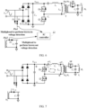
- FIG. 1 is a schematic diagram of a power switching converter for detecting a working voltage of a direct current bus to perform brown in/out control according to a first solution.
- the power switching converter includes an AC/DC conversion circuit 11, a switching conversion module 12, an IC controller 13, and a load RL.
- the AC/DC conversion circuit 11 is a full-wave rectifier structure, including a capacitor C in , a diode D 4 , a diode D 5 , a diode D 6 , and a diode D 7 .
- the capacitor C in is denoted as a first capacitor
- the diode D 4 , the diode D 5 , the diode D 6 , and the diode D 7 are respectively denoted as a fourth diode, a fifth diode, a sixth diode, and a seventh diode.
- An anode of the diode D 6 is connected in series to a cathode of the diode D 4 , and a first common node after the series connection is connected to a first input terminal of an alternating current power supply.
- An anode of the diode D 5 is connected in series to a cathode of the diode D 7 , and a second common node after the series connection is connected to a second input terminal of the alternating current power supply.
- a cathode of the diode D 6 is coupled to a cathode of the capacitor C in after being connected in parallel to a cathode of the diode D 5 .
- An anode of the diode D 7 is coupled to an anode of the capacitor C in and is grounded after being connected in parallel to an anode of the diode D 4 .
- the first input terminal of the alternating current power supply may be a live wire L, and the second input terminal may be a neutral wire N.
- the first input terminal of the alternating current power supply may be a neutral wire N, and the second input terminal may be a live wire L. This is not specifically limited herein.
- the AC/DC conversion circuit 11 converts a negative voltage component of an input alternating current voltage V in into a positive voltage by using the full-wave rectifier structure, and then rectifies the input alternating current voltage into a direct current pulse voltage, and then smoothens a waveform by using charging and discharging functions of the capacitor C in , to rectify the alternating current voltage into a direct current voltage.
- the switching conversion module 12 is an asymmetrical half-bridge (asymmetrical half-bridge, AHB) flyback structure, including a switching transistor Q L , a switching transistor Q H , a capacitor C r , and a transformer T .
- AHB asymmetrical half-bridge
- the switching transistor Q L and the switching transistor are connected in series and coupled at both terminals of the AC/DC conversion circuit 11.
- a primary-side winding of the transformer T is connected in parallel at both terminals of the switching transistor Q L by using the capacitor C r .
- the transformer T may be equivalent to an excitation inductor L m , a leakage inductor L r , and an ideal transformer T '.
- the transformer T includes two secondary-side windings. In the figure, ".” is used to indicate a dotted terminal of the primary-side winding Z p , the first secondary-side winding Z s , and the second secondary-side winding Z a .
- a first terminal of the secondary-side winding Z s is coupled to a source of the switching transistor SR, and a drain of the switching transistor SR is coupled to a first terminal of the capacitor C 0 and a first terminal of the load R L .
- a diode may be used instead of the switching transistor SR.
- a second terminal of the capacitor C 0 and a second terminal of the load R L are coupled to a second terminal of the secondary-side winding Z s and are grounded.
- the capacitor C 0 may reduce a ripple of a first output voltage V 0 of the transformer T.
- a first terminal of the alternating current power supply is connected to an anode of a diode D 1
- a second terminal of the alternating current power supply is connected to an anode of a diode D 2
- a common output terminal after a cathode of the diode D 1 and a cathode of the diode D 2 are connected in parallel, is a pin Pin1.
- the pin Pin1 is connected to the IC controller 13, and may supply power to the IC controller 13. After the alternating current power supply is started, the IC controller 13 is powered on.
- the switching conversion module 12 further includes a monitoring circuit 122 and an auxiliary circuit 121.
- the IC controller 13 is connected to a pin Pin3 of the monitoring circuit 122, and the IC controller 13 may detect a direct current bus voltage V bus in the monitoring circuit 122, to output a control instruction to implement brown in/out function control.
- a voltage on the pin Pin3 detected by the IC controller 13 is the direct current bus voltage V bus of the switching conversion module 12.
- a control instruction is output, so that the switching transistor Q H is turned on, and a current increases in a clockwise direction indicated by an arrow in FIG. 1 , and the switching conversion module 12 enters an operating state.
- a second control instruction is output, to turn off the switching transistor Q H and the switching transistor Q L , to shut down operation of the circuit and implement a brown in/out function.
- a function performed by the auxiliary circuit 121 may be auxiliary power supplying and implementation of a zero voltage switch (zero voltage switch, ZVS) function.
- the auxiliary circuit 121 includes the secondary-side winding Z a of the transformer T .
- a first terminal of the secondary-side winding Z a is coupled to an anode of the diode D 3 .
- a cathode of the diode D 3 is coupled to a first terminal of the capacitor C 1 .
- a second terminal of the capacitor C 1 is coupled to a second terminal of the secondary-side winding Z a and is grounded.
- a pin Pin2 is disposed at a common node between the anode of the diode D 3 and the first terminal of the secondary-side winding Z a .
- Pin2 is connected to the IC controller 13 to provide auxiliary voltage detection and the zero voltage switch (zero voltage switch, ZVS) function for the IC controller 13.
- the ZVS function is to turn on a switching transistor when a voltage at both terminals of the switching transistor drops to 0 V Through the ZVS function, turn-on loss of the switching transistor can be minimized.
- a disadvantage of the first solution is that the additional monitoring circuit 122 needs to be added to implement brown in/out for an asymmetrical half-bridge flyback topological structure, to obtain the direct current bus voltage V bus of the switching conversion module 12.
- the IC controller 13 needs to detect the voltage on the pin Pin3 to obtain the direct current bus voltage V bus , to output the control instruction to turn on or off the operation of the switching conversion module 12.
- the solution can implement the brown in/out function, system costs are increased.
- An embodiment of this application provides a switching conversion circuit.
- the pin Pin1 is used as a first detection terminal, and the IC controller 13 is connected to the pin Pin1.
- a first control instruction is output, to implement a control function of brown in.
- the pin Pin2 is used as a second detection terminal.
- a second control instruction is output, to implement a control function of brown out.
- the voltage value for exiting normal operation is less than the lowest input voltage value for entering normal operation, and a voltage difference between the two is not less than a specified threshold.
- the switching conversion circuit provided in this embodiment of this application does not need to add the additional monitoring circuit 122 to detect the working voltage of the direct current bus in the switching conversion module 12, but time-division multiplexes the pin Pin1 as the first detection terminal and time-division multiplexes the pin Pin2 as the second detection terminal, to implement the control function of brown in/out while performing functions such as power supplying and ZVS.
- FIG. 2 is a schematic diagram of a switching conversion circuit according to this embodiment of this application.
- a voltage value V bus of the direct current bus is equal to a value of an alternating current voltage V in input on an alternating current power supply side. Therefore, the value of the alternating current voltage V in may be used as a voltage required for entering normal operation by the switching conversion module 12.
- the pin Pin1 may be used as the first detection terminal.
- the IC controller 13 detects a value of a voltage output by the pin Pin1, outputs the first control instruction when the value of the voltage output by the pin Pin1 reaches a preset lowest voltage required for entering normal operation, to turn on Q L and enable the switching conversion module 12 to enter the operating state, to implement the control function of brown in.
- the preset lowest input voltage value required for entering normal operation may be denoted as a first threshold.
- a voltage output by the pin Pin1 is denoted as a first voltage
- a value of the first voltage is the value of the alternating current voltage V in input on the alternating current power supply side.
- the IC controller 13 When the switching conversion module 12 has entered the operating state, the IC controller 13 performs zero voltage switch (zero voltage switch, ZVS) control on the switching conversion module by detecting a value of a second voltage output by the second detection terminal of the second secondary-side winding of the transformer.
- ZVS zero voltage switch
- the IC controller may turn off a first switching transistor and a second switching transistor based on the value of the voltage output by the first detection terminal, so that the switching conversion module 12 stops supplying power to the load. For example, the IC controller detects the value of the voltage output by the first detection terminal. When the value of the voltage output by the first detection terminal is less than the preset voltage value for exiting normal operation, the IC controller outputs the second control instruction, to turn off the first switching transistor and the second switching transistor. In this way, the control function of brown out is implemented.
- the preset voltage value for exiting normal operation may be denoted as a second threshold.
- the voltage output by the first detection terminal after the switching conversion module 12 enters the operating state is denoted as a third voltage.
- the switching conversion circuit provided in this embodiment of this application may perform precise brown out control by monitoring a voltage output by the second secondary-side winding Z a of the transformer T.
- the IC controller performs, based on a voltage output by the second detection terminal Pin2, brown out control while implementing the ZVS function, where the output voltage of the pin Pin2 may be used as a detection reference voltage for overvoltage and undervoltage protection, and after the voltage passes through a diode and a capacitor, low-voltage direct current power supplying may be further performed on a chip such as the IC controller.
- the IC controller 13 In a process in which the IC controller 13 detects the value of the second voltage output by the pin PIN2, the IC controller 13 periodically turns on/off the switching transistor based on a switching period, so that the switching transistor Q H and the switching transistor Q L operate alternately. Therefore, in this process, the IC controller 13 can detect voltages V 2 _ H and V 2 _ L that are alternately changed and output by the pin Pin2, so that the value of the direct current bus voltage V bus can be obtained in each switching period.
- the IC controller 13 detects the value of the voltage output by the pin Pin2, and obtains the value V bus of the direct current bus voltage in the switching conversion module 12 based on a first value V 2 _ L and a second value V 2_H that are output by the pin Pin2 in different states of the switching transistor and a ratio of a quantity of turns of the primary-side winding to a quantity of turns of the second secondary-side winding in the transformer T, to perform brown out control and stop the switching conversion module 12 from operating.
- the following analyzes a brown out control principle by using FIG. 3 and FIG. 4 .
- FIG. 3 is a state diagram of a switching conversion circuit according to an embodiment of this application when Q H is turned off and Q L is turned on.
- a quantity of turns of a primary-side winding Z p of the transformer T is N p
- a quantity of turns of a secondary-side winding Z s is N S
- a quantity of turns of a secondary-side winding Z a is N a
- a rating working voltage of a load R L is V 0 .
- FIG. 4 is a state diagram of a switching conversion circuit according to an embodiment of this application when Q H is turned on and Q L is turned off.
- the direct current bus voltage of the switching conversion module 12 is V bus
- a voltage at both terminals of the resonance capacitor C r is nV 0
- the voltage at both terminals of the primary-side winding Z p of the transformer T is ( V bus - nV 0 )
- V bus V 2 _ L ⁇ V 2 _ H * N p / N a
- the IC controller 13 separately detects the voltage value V 2_H output by the pin Pin2 when Q H is turned on and Q L is turned off, and the voltage value V 2 _ L output by the pin Pin2 when Q H is turned off and Q L is turned on. Based on the values V 2_H and V 2_L as well as the ratio of the quantity of turns of the primary-side winding to the quantity of turns of the second secondary-side winding, the IC controller 13 determines the value of the direct current bus voltage V bus in the switching conversion module 12, and when the value of V bus is lower than the specified voltage value for exiting normal operation, outputs a second control instruction, to shut down operation of the circuit and implement the brown out control function.
- the direct current bus voltage V bus of the switching conversion module 12 is obtained by time-division multiplexing the pin Pin2 as a brown out voltage detection terminal, which is a hysteresis process.
- FIG. 5 is a schematic diagram of a hysteresis of a switching conversion circuit according to an embodiment of this application.
- V th_brownin is the lowest input voltage value for entering normal operation, that is, the first threshold.
- V th_brownout is the voltage value for exiting normal operation, that is, the second threshold.
- V 1 is the voltage value of the pin Pin1.
- V bus is the direct current bus voltage value.
- a value of the second threshold V th_brownout is less than a value of the first threshold V th _ browmin , and a voltage difference between the value of the second threshold V th_brownout and the value of the first threshold V th_brownin is not less than a specified voltage difference threshold.
- the switching conversion circuit includes a power module 21 and the switching conversion module 12.
- An output terminal of the power module 21 is coupled to the switching conversion module 12, and the power module 21 provides a direct current voltage to supply power to the switching conversion module 12.
- the output terminal of the power module 21 is coupled to the power module 14, and the power module 14 is used as a first detection unit.
- An output terminal Pin1 of the power module 14 is connected to the IC controller 13 to supply power to the IC controller 13.
- the switching transistor Q L is denoted as a first switching transistor
- the switching transistor Q H is denoted as a second switching transistor.
- the switching transistor Q L and the switching transistor Q H are connected in series and coupled at both terminals of the power module 21.
- the primary-side winding Z p of the transformer T is coupled at both terminals of the switching transistor Q L by using the first capacitor C r , which may be denoted as an AHB topological structure of a lower half-bridge arm.
- the secondary-side winding Z s of the transformer is coupled at both terminals of the load by using the switching transistor SR.
- the auxiliary circuit 121 disposed based on the second secondary-side winding Z a of the transformer is used as a second detection unit.
- An output terminal Pin2 of the auxiliary circuit 121 is connected to the IC controller 13.
- the IC controller 13 performs brown in control on the switching conversion module 12 based on a voltage output by Pin1, so that the switching converter enters the operating state.
- the IC controller 13 performs brown out control on the switching conversion module 12 based on a voltage output by Pin2, so that the switching converter stops operating.
- Pin1 is denoted as a first detection terminal
- Pin2 is denoted as a second detection terminal.
- the voltage output by Pin1 is denoted as a first voltage
- the voltage output by Pin2 is denoted as a second voltage.
- a capacitor C in is denoted as a first capacitor
- a capacitor C r is denoted as a second capacitor
- a capacitor C 1 is denoted as a third capacitor
- a capacitor C 0 is denoted as a fourth capacitor.
- the power module 21 may be an AC/DC converter, to rectify an alternating current voltage output by the alternating current power supply into a direct current voltage to supply power.
- the power module may alternatively be a direct current power supply, and includes at least one of the following apparatuses: an energy storage battery (such as a nickel-cadmium battery, a nickel-metal hydride battery, a lithium ion battery, and a lithium polymer battery), a solar cell, another direct current/direct current converter (direct-current/direct-current converter, DC/DC), such as a buck converter, a boost converter, and a buck-boost converter, to directly output a direct current voltage to supply power.
- an energy storage battery such as a nickel-cadmium battery, a nickel-metal hydride battery, a lithium ion battery, and a lithium polymer battery
- DC/DC direct current/direct current converter
- buck converter buck converter
- boost converter boost converter
- buck-boost converter buck-boost
- the IC controller 13 detects a value of the first voltage output by Pin1 before the switching conversion module enters the operating state; and when the value of the first voltage reaches a first threshold, outputs a first control instruction, to turn on the switching transistor Q L , so that the switching conversion module 12 enters the operating state to supply power to the load.
- the first threshold is a preset lowest input voltage value for entering normal operation.
- the value of the first voltage is a value of an alternating current input voltage, and a peak value of the first voltage may be used as a reference value.
- the IC controller 13 detects, in an operating state in which the switching transistor Q L is turned on and the switching transistor Q H is turned off, a value of the second voltage output by Pin2 to obtain a first value; detects, in an operating state in which the switching transistor Q L is turned off and the switching transistor Q H is turned on, a value of the second voltage output by Pin2 to obtain a second value; obtains a value of a direct current bus voltage in an asymmetrical half-bridge flyback circuit based on the first value, the second value, and a ratio of a quantity of turns of the primary-side winding to a quantity of turns of the second secondary-side winding; and when the value of the direct current bus voltage is less than a second threshold, outputs a second control instruction, to turn off the switching transistor Q L and the switching transistor Q H , where the second threshold is a specified voltage value for exiting normal operation.
- the switching conversion circuit provided in this embodiment of this application is not limited to an AHB topological structure in which the transformer and the switching transistor Q L are coupled in parallel, and is also applicable to an AHB topological structure in which the transformer and the switching transistor Q H are coupled in parallel.
- the AHB structure in which the transformer and the switching transistor Q H are coupled in parallel may be denoted as an AHB topological structure of an upper half-bridge arm.
- FIG. 6 is a circuit diagram of an AHB topological structure of an upper half-bridge arm in a switching conversion circuit according to an embodiment of this application.
- the primary-side winding of the transformer is coupled at both terminals of the switching transistor Q H by using the capacitor C r .
- the IC controller 13 detects a value of the first voltage output by Pin1 before the switching conversion module enters the operating state; and when the value of the first voltage reaches the first threshold, outputs a first control instruction, to turn on the switching transistor Q H , so that the switching conversion module 12 enters the operating state to supply power to the load.
- the IC controller 13 detects, in an operating state in which the switching transistor Q L is turned off and the switching transistor Q H is turned on, a value of the second voltage output by Pin2 to obtain a first value; detects, in an operating state in which the switching transistor Q L is turned on and the switching transistor Q H is turned off, a value of the second voltage output by Pin2 to obtain a second value; obtains a value of the direct current bus voltage in the asymmetrical half-bridge flyback circuit based on the first value, the second value, and the ratio of the quantity of turns of the primary-side winding to the quantity of turns of the second secondary-side winding; and when the value of the direct current bus voltage is less than the second threshold, outputs a second control instruction, to turn off the switching transistor Q L and the switching transistor Q H .
- FIG. 7 is a state diagram of a detection circuit of an AHB structure of an upper half-bridge arm when Q H is turned on and Q L is turned off.
- FIG. 8 is a state diagram of a detection circuit of an AHB structure of an upper half-bridge arm when Q H is turned off and Q L is turned on.
- the direct current bus voltage of the main circuit of the switching conversion module 12 is V bus
- a voltage at both terminals of the resonance capacitor C r is nV 0
- the voltage at both terminals of the primary-side winding Z p of the transformer T is ( V bus - nV 0 )
- V bus V 2 _ H ⁇ V 2 _ L * N p / N a
- the IC controller 13 detects the voltage value V 2_H of the pin Pin2 when Q H is turned on and Q L is turned off, and the voltage value V 2 _ L of the pin Pin2 when Q H is turned off and Q L is turned on; determines a value of the direct current bus voltage V bus of the main circuit of the switching conversion module 12 based on a difference between V 2_H and V 2 _ L ; and when a value of V bus is less than the second threshold, turns off Q H and Q L , to stop supplying power to the load and implement the control function of brown out.
- the AC/DC conversion circuit 11 may alternatively be a half-wave rectifier structure.
- FIG. 9 is a half-wave rectifier structure of an alternating current power supply in a switching conversion circuit according to an embodiment of this application.
- the half-wave rectifier structure of the AC/DC conversion circuit 11 includes a first capacitor C in and a diode D 8 .
- An anode of the diode D 8 is coupled to a first input terminal of the alternating current power supply, and a cathode of the diode D 8 is coupled to a cathode of the capacitor C in .
- An anode of the capacitor C in is coupled to a second input terminal of the alternating current power supply and grounded.
- the AC/DC conversion circuit 11 rectifies an input alternating current voltage V in into a direct current pulse voltage by using the half-wave rectifier circuit of the diode, and smoothens a waveform by using charging and discharging functions of the capacitor C in , to rectify the alternating current voltage into a direct current voltage.
- the IC controller 13 detects a value of the first voltage output by Pin1 before the switching conversion module enters the operating state; and when the value of the first voltage reaches the first threshold, outputs a first control instruction, to turn on the switching transistor Q L , so that the switching conversion module 12 enters the operating state to supply power to the load.
- the IC controller 13 detects, in an operating state in which the switching transistor Q L is turned off and the switching transistor Q H is turned on, a value of the second voltage output by Pin2 to obtain a first value; detects, in an operating state in which the switching transistor Q L is turned on and the switching transistor Q H is turned off, a value of the second voltage output by Pin2 to obtain a second value; obtains a value of the direct current bus voltage in the asymmetrical half-bridge flyback circuit based on the first value, the second value, and the ratio of the quantity of turns of the primary-side winding to the quantity of turns of the second secondary-side winding; and when the value of the direct current bus voltage is less than the second threshold, outputs a second control instruction, to turn off the switching transistor Q L and the switching transistor Q H .
- Control principles of the switching conversion module 12 and brown in/out are the same as those in the foregoing implementations, and are not repeated herein.
- An embodiment of this application provides a control method for a switching conversion circuit. The method is implemented based on the switching conversion circuit in one of the foregoing embodiments, and is performed by an IC controller 13.
- the IC controller 13 When a primary-side winding of a transformer is coupled to both terminals of a switching transistor Q L by using a first capacitor, the IC controller 13 turns on the switching transistor Q L or a switching transistor Q H based on a value of a first voltage output by a first detection terminal, so that a switching conversion module 12 enters an operating state to supply power to a load; and turns off the switching transistor Q L and the switching transistor Q H based on a value of a second voltage output by a second detection terminal, so that the switching conversion module 12 stops supplying power to the load.
- the IC controller 13 detects a value of the first voltage output by the first detection terminal; when the value of the first voltage reaches a first threshold, outputs a first control instruction, so that the switching converter enters the operating state to supply power to the load.
- the first threshold is a preset lowest input voltage value for entering normal operation.
- the first voltage is a value of an alternating current input voltage.
- the IC controller 13 detects, in an operating state in which the switching transistor Q L is turned on and the switching transistor Q H is turned off, a value of the second voltage output by the second detection terminal, to obtain a first value; detects, in an operating state in which the switching transistor Q L is turned off and the switching transistor Q H is turned on, a value of the second voltage output by the second detection terminal, to obtain a second value; obtains a value of a direct current bus voltage in an asymmetrical half-bridge flyback circuit based on the first value, the second value, and a ratio of a quantity of turns of the primary-side winding to a quantity of turns of a second secondary-side winding; when the value of the direct current bus voltage is less than a second threshold, outputs a second control instruction, to turn off the switching transistor Q L and the switching transistor Q H , where the second threshold is a specified voltage value for exiting normal operation.
- the IC controller 13 detects a value of the first voltage output by the first detection terminal; when the value of the first voltage reaches a first threshold, outputs a first control instruction, to turn on the switching transistor Q H , so that the switching conversion module 12 enters the operating state to supply power to the load.
- the IC controller 13 detects, in an operating state in which the switching transistor Q L is turned off and the switching transistor Q H is turned on, a value of the second voltage output by the second detection terminal, to obtain a first value; detects, in an operating state in which the switching transistor Q L is turned on and the switching transistor Q H is turned off, a value of the second voltage output by the second detection terminal, to obtain a second value; obtains a value of a direct current bus voltage in an asymmetrical half-bridge flyback circuit based on the first value, the second value, and a ratio of a quantity of turns of the primary-side winding to a quantity of turns of the second secondary-side winding; and when the value of the direct current bus voltage is less than a second threshold, outputs a second control instruction, to turn off the switching transistor Q L and the switching transistor Q H .
- the method further includes performing zero voltage switch control on the switching conversion module by using the value of the second voltage output by the second detection terminal.
- the alternating current power supply described in embodiments of this application may be a singlephase alternating current voltage of a power grid or an alternating current voltage output by another alternating current power supply.
- the load described in embodiments of this application may be a mobile phone terminal, an energy storage battery, another DC/DC converter, a DC/AC converter, and/or the like.
- a switching transistor Q H and a switching transistor Q L are metal-oxide-semiconductor field-effect transistors (metal-oxide-semiconductor field-effect transistor, MOSFET) is used as an example for description. It should be understood that each switching transistor may alternatively be another semiconductor device, such as an insulated gate bipolar transistor (insulated gate bipolar transistor, IGBT).
- MOSFET metal-oxide-semiconductor field-effect transistor
- the IC controller described in this application may be a central processing unit (central processing unit, CPU), another general purpose processor, a digital signal processor (digital signal processor, DSP), an applicationspecific integrated circuit (application specific integrated circuited circuit, ASIC), a field-programmable gate array (field-programmable gate array, FPGA) or another programmable logic device, a discrete gate or transistor logic device, a discrete hardware component, or the like.
- CPU central processing unit
- DSP digital signal processor
- ASIC application specific integrated circuited circuit
- FPGA field-programmable gate array
- FPGA field-programmable gate array
- the load may be a mobile phone terminal
- the alternating current power supply may be a power grid alternating current voltage.
- the AC/DC converter (including an uncontrolled rectifier and a DC/DC converter) converts an input alternating current voltage of the power grid into a direct current voltage.
- the IC controller monitors a working voltage in the circuit to output a control instruction, and performs brown in/out control on a power switch controller, to convert the direct current voltage output by the AC/DC converter into a specified direct current voltage value, for example, 5 V and 10 V
- the AC/DC converter (including an uncontrolled rectifier and a DC/DC converter) and the IC controller may be disposed in a power adapter.
Landscapes
- Engineering & Computer Science (AREA)
- Power Engineering (AREA)
- Dc-Dc Converters (AREA)
Description
- This application relates to the field of power supply technologies, and in particular to a switching conversion circuit and a control method.
- A. Medina-Garcia et al, "Advanced Control Methods for Asymmetrical Half-Bridge Flyback", IEEE Transactions on Power Electronics Vol. 36, No. 11, November 2021, pages 13139-13148, describes that in the article, a power converter based on an asymmetrical half-bridge flyback topology is analyzed and optimized for small form factor and fast-charging power adaptors. It is described that two resonant control methods, taking advantage of the forward and flyback characteristics of the converter, as well as the benefits of each of them depending of the operation point are discussed. It is described that the analysis is nourished with the equivalent circuits in each phase of operation and the equations that define them. It is described that a proposed zero voltage resonant valley switching control method for the mentioned converter; in this case, it is operated similarly to a flyback converter, allowing safe output voltage ramp up, which is one of the challenges that has limited the usage of this topology up to now. The manuscript also describes how to achieve high efficiency and power density using zero-voltage switching and zero-current switching techniques over the full range of the input voltage and the output load.
- With deepening of energy saving, requirements of international standards for features such as efficiency of power supply products are becoming increasingly higher. A switch mode power supply usually needs to determine an operating state of the power supply based on a voltage on an input side, that is, a brown in/out function. Brown in refers to turning on a circuit when the voltage on the input side of the power supply reaches a specified operable voltage threshold. Brown out refers to turning off the circuit when the voltage on the input side of the power supply is lower than the specified operable voltage threshold.
- Brown in/out is actually used to control the circuit to turn on and off, which can protect the circuit when the input voltage is extremely low. An effective and fast implementation of the brown in/out function is a basic feature of the switch mode power supply.
- It is very easy to implement the brown in/out function after a specific value of the voltage on the input side is known. However, for a power controller, when a working voltage is detected to output a control instruction to perform brown in/out control, it is expected to reduce a quantity of pins and peripheral circuits as much as possible. Therefore, a switching conversion circuit and a control method are urgently needed, so that the brown in/out function can still be implemented without adding an additional input voltage detection pin.
- To resolve the foregoing problem, embodiments of this application provide a switching conversion circuit and a control method.
- Appended
claim 1 defines a switching conversion circuit. Appendedclaim 12 defines a control method implemented based on a switching conversion circuit. The invention and its scope of protection is defined by these independent claims. advantageous aspects of the present invention are given by the dependent claims. - The following briefly describes the accompanying drawings used to describe embodiments or the conventional technology.
-
FIG. 1 is a schematic diagram of a power switching converter for detecting a working voltage of a direct current bus to perform brown in/out control according to a first solution; -
FIG. 2 is a schematic diagram of an AHB topological structure in which a transformer and a switching transistor QL in a switching conversion circuit are connected in parallel according to an embodiment of this application; -
FIG. 3 is a state diagram of the AHB topological structure shown inFIG. 2 of this application when a switching transistor QH is turned off and a switching transistor QL is turned on; -
FIG. 4 is a state diagram of the AHB topological structure shown inFIG. 2 of this application when a switching transistor QH is turned on and a switching transistor QL is turned off; -
FIG. 5 is a schematic diagram of a hysteresis of a switching conversion circuit according to an embodiment of this application; -
FIG. 6 is a schematic diagram of an AHB topological structure in which a transformer and a switching transistor QH in a switching conversion circuit are connected in parallel according to an embodiment of this application; -
FIG. 7 is a state diagram of a detection circuit with the AHB topological structure inFIG. 6 when a switching transistor QH is turned on and a switching transistor QL is turned off; -
FIG. 8 is a state diagram of a detection circuit with the AHB topological structure inFIG. 6 when a switching transistor QH is turned off and a switching transistor QL is turned on; and -
FIG. 9 is a half-wave rectifier structure of an alternating current power supply in a switching conversion circuit according to an embodiment of this application. - The following describes the technical solutions in embodiments of this application with reference to the accompanying drawings in embodiments of this application.
- It should be noted that "coupling" described in this application means a direct or indirect connection. For example, a connection between A and B may be a direct connection between A and B, or may be an indirect connection between A and B by using one or more other electrical components. For example, A is directly connected to C, and C is directly connected to B, so that a connection between A and B is implemented by using C.
- The foregoing is an example description of a use scenario of the embodiment of this application, and is not exhaustive. It should be understood that a switching conversion circuit and a control method for brown in/out control performed by an IC controller in the embodiment of this application can be applied to any scenario in which a supply voltage needs to be converted.
-
FIG. 1 is a schematic diagram of a power switching converter for detecting a working voltage of a direct current bus to perform brown in/out control according to a first solution. As shown inFIG. 1 , the power switching converter includes an AC/DC conversion circuit 11, aswitching conversion module 12, anIC controller 13, and a load RL. - The AC/
DC conversion circuit 11 is a full-wave rectifier structure, including a capacitor Cin , a diode D 4, a diode D 5 , a diode D 6, and a diode D 7. The capacitor Cin is denoted as a first capacitor, the diode D 4, the diode D 5, the diode D 6, and the diode D 7 are respectively denoted as a fourth diode, a fifth diode, a sixth diode, and a seventh diode. An anode of the diode D 6 is connected in series to a cathode of the diode D 4, and a first common node after the series connection is connected to a first input terminal of an alternating current power supply. An anode of the diode D 5 is connected in series to a cathode of the diode D 7, and a second common node after the series connection is connected to a second input terminal of the alternating current power supply. A cathode of the diode D 6 is coupled to a cathode of the capacitor Cin after being connected in parallel to a cathode of the diode D 5 . An anode of the diode D 7 is coupled to an anode of the capacitor Cin and is grounded after being connected in parallel to an anode of the diode D 4. The first input terminal of the alternating current power supply may be a live wire L, and the second input terminal may be a neutral wire N. Alternatively, the first input terminal of the alternating current power supply may be a neutral wire N, and the second input terminal may be a live wire L. This is not specifically limited herein. - The AC/
DC conversion circuit 11 converts a negative voltage component of an input alternating current voltage Vin into a positive voltage by using the full-wave rectifier structure, and then rectifies the input alternating current voltage into a direct current pulse voltage, and then smoothens a waveform by using charging and discharging functions of the capacitor Cin, to rectify the alternating current voltage into a direct current voltage. - The
switching conversion module 12 is an asymmetrical half-bridge (asymmetrical half-bridge, AHB) flyback structure, including a switching transistor QL , a switching transistor QH , a capacitor Cr , and a transformer T. InFIG. 1 , the switching transistor QL and the switching transistor are connected in series and coupled at both terminals of the AC/DC conversion circuit 11. A primary-side winding of the transformer T is connected in parallel at both terminals of the switching transistor QL by using the capacitor Cr . - The transformer T may be equivalent to an excitation inductor Lm , a leakage inductor Lr, and an ideal transformer T'. The transformer T includes two secondary-side windings. In the figure, "." is used to indicate a dotted terminal of the primary-side winding Zp , the first secondary-side winding Zs , and the second secondary-side winding Za .
- A first terminal of the secondary-side winding Zs is coupled to a source of the switching transistor SR, and a drain of the switching transistor SR is coupled to a first terminal of the capacitor C 0 and a first terminal of the load RL . Alternatively, a diode may be used instead of the switching transistor SR. A second terminal of the capacitor C 0 and a second terminal of the load RL are coupled to a second terminal of the secondary-side winding Zs and are grounded. The capacitor C 0 may reduce a ripple of a first output voltage V 0 of the transformer T.
- In a
power module 14, a first terminal of the alternating current power supply is connected to an anode of a diode D 1, a second terminal of the alternating current power supply is connected to an anode of a diode D 2, and a common output terminal after a cathode of the diode D 1 and a cathode of the diode D 2 are connected in parallel, is a pin Pin1. - The pin Pin1 is connected to the
IC controller 13, and may supply power to theIC controller 13. After the alternating current power supply is started, theIC controller 13 is powered on. - In the circuit shown in
FIG. 1 , theswitching conversion module 12 further includes amonitoring circuit 122 and anauxiliary circuit 121. TheIC controller 13 is connected to a pin Pin3 of themonitoring circuit 122, and theIC controller 13 may detect a direct current bus voltage Vbus in themonitoring circuit 122, to output a control instruction to implement brown in/out function control. - For example, after the
IC controller 13 is powered on, and when theswitching conversion module 12 is still in a non-operating state, a voltage on the pin Pin3 detected by theIC controller 13 is the direct current bus voltage Vbus of theswitching conversion module 12. When the voltage on the pin PIN3 reaches or exceeds a voltage for normal operation, a control instruction is output, so that the switching transistor QH is turned on, and a current increases in a clockwise direction indicated by an arrow inFIG. 1 , and theswitching conversion module 12 enters an operating state. When theIC controller 13 detects that the voltage Vbus on the pin Pin3 is lower than the voltage for normal operation, a second control instruction is output, to turn off the switching transistor QH and the switching transistor QL, to shut down operation of the circuit and implement a brown in/out function. - In the operating state, a function performed by the
auxiliary circuit 121 may be auxiliary power supplying and implementation of a zero voltage switch (zero voltage switch, ZVS) function. Theauxiliary circuit 121 includes the secondary-side winding Za of the transformer T . A first terminal of the secondary-side winding Za is coupled to an anode of the diode D 3. A cathode of the diode D 3 is coupled to a first terminal of the capacitor C 1 . A second terminal of the capacitor C 1 is coupled to a second terminal of the secondary-side winding Za and is grounded. A pin Pin2 is disposed at a common node between the anode of the diode D 3 and the first terminal of the secondary-side winding Za . Pin2 is connected to theIC controller 13 to provide auxiliary voltage detection and the zero voltage switch (zero voltage switch, ZVS) function for theIC controller 13. The ZVS function is to turn on a switching transistor when a voltage at both terminals of the switching transistor drops to 0 V Through the ZVS function, turn-on loss of the switching transistor can be minimized. - A disadvantage of the first solution is that the
additional monitoring circuit 122 needs to be added to implement brown in/out for an asymmetrical half-bridge flyback topological structure, to obtain the direct current bus voltage Vbus of theswitching conversion module 12. TheIC controller 13 needs to detect the voltage on the pin Pin3 to obtain the direct current bus voltage Vbus, to output the control instruction to turn on or off the operation of theswitching conversion module 12. Although the solution can implement the brown in/out function, system costs are increased. - An embodiment of this application provides a switching conversion circuit. For the asymmetrical half-bridge flyback topological structure of the
switching conversion module 12, the pin Pin1 is used as a first detection terminal, and theIC controller 13 is connected to the pin Pin1. When it is determined, by detecting a voltage value of the pin Pin1, that a current voltage reaches or exceeds a preset lowest input voltage value for entering normal operation, a first control instruction is output, to implement a control function of brown in. The pin Pin2 is used as a second detection terminal. When it is determined, by detecting a voltage value of the pin Pin2, that the current voltage is lower than a preset voltage value for exiting normal operation, a second control instruction is output, to implement a control function of brown out. The voltage value for exiting normal operation is less than the lowest input voltage value for entering normal operation, and a voltage difference between the two is not less than a specified threshold. - The switching conversion circuit provided in this embodiment of this application does not need to add the
additional monitoring circuit 122 to detect the working voltage of the direct current bus in theswitching conversion module 12, but time-division multiplexes the pin Pin1 as the first detection terminal and time-division multiplexes the pin Pin2 as the second detection terminal, to implement the control function of brown in/out while performing functions such as power supplying and ZVS. This reduces a quantity of peripheral circuits and output terminals of theswitching conversion module 12, reduces a quantity of pins detected by theIC controller 13, and reduces the system costs. - The following describes a detection principle of a switching converter provided in this embodiment of this application with reference to
FIG. 2 . -
FIG. 2 is a schematic diagram of a switching conversion circuit according to this embodiment of this application. As shown inFIG. 2 , when detection is performed when theswitching conversion module 12 stops operating, because there is basically no loss of theswitching conversion module 12, it may be considered that a voltage value Vbus of the direct current bus is equal to a value of an alternating current voltage Vin input on an alternating current power supply side. Therefore, the value of the alternating current voltage Vin may be used as a voltage required for entering normal operation by theswitching conversion module 12. - For example, the pin Pin1 may be used as the first detection terminal. The
IC controller 13 detects a value of a voltage output by the pin Pin1, outputs the first control instruction when the value of the voltage output by the pin Pin1 reaches a preset lowest voltage required for entering normal operation, to turn on QL and enable theswitching conversion module 12 to enter the operating state, to implement the control function of brown in. The preset lowest input voltage value required for entering normal operation may be denoted as a first threshold. When theswitching conversion module 12 stops operating, a voltage output by the pin Pin1 is denoted as a first voltage, and a value of the first voltage is the value of the alternating current voltage Vin input on the alternating current power supply side. - When the
switching conversion module 12 has entered the operating state, theIC controller 13 performs zero voltage switch (zero voltage switch, ZVS) control on the switching conversion module by detecting a value of a second voltage output by the second detection terminal of the second secondary-side winding of the transformer. An implementation process of the ZVS is not significantly related to the patent of this application, and is not discussed herein. - After the
switching conversion module 12 enters the operating state, the IC controller may turn off a first switching transistor and a second switching transistor based on the value of the voltage output by the first detection terminal, so that theswitching conversion module 12 stops supplying power to the load. For example, the IC controller detects the value of the voltage output by the first detection terminal. When the value of the voltage output by the first detection terminal is less than the preset voltage value for exiting normal operation, the IC controller outputs the second control instruction, to turn off the first switching transistor and the second switching transistor. In this way, the control function of brown out is implemented. The preset voltage value for exiting normal operation may be denoted as a second threshold. The voltage output by the first detection terminal after theswitching conversion module 12 enters the operating state is denoted as a third voltage. - However, after the
switching conversion module 12 enters the operating state, because a main circuit of theswitching conversion module 12 already operates, brown out control performed by using the value of the voltage output by the first detection terminal as a detection voltage is not accurate, and does not meet power supply requirements of some loads or chips with high safety or accuracy requirements. - The switching conversion circuit provided in this embodiment of this application may perform precise brown out control by monitoring a voltage output by the second secondary-side winding Za of the transformer T.
- In a possible implementation, the IC controller performs, based on a voltage output by the second detection terminal Pin2, brown out control while implementing the ZVS function, where the output voltage of the pin Pin2 may be used as a detection reference voltage for overvoltage and undervoltage protection, and after the voltage passes through a diode and a capacitor, low-voltage direct current power supplying may be further performed on a chip such as the IC controller.
- In a process in which the
IC controller 13 detects the value of the second voltage output by the pin PIN2, theIC controller 13 periodically turns on/off the switching transistor based on a switching period, so that the switching transistor QH and the switching transistor QL operate alternately. Therefore, in this process, theIC controller 13 can detect voltages V 2_H and V 2_L that are alternately changed and output by the pin Pin2, so that the value of the direct current bus voltage Vbus can be obtained in each switching period. - In a possible implementation, the
IC controller 13 detects the value of the voltage output by the pin Pin2, and obtains the value Vbus of the direct current bus voltage in theswitching conversion module 12 based on a first value V 2_L and a second value V2_H that are output by the pin Pin2 in different states of the switching transistor and a ratio of a quantity of turns of the primary-side winding to a quantity of turns of the second secondary-side winding in the transformer T, to perform brown out control and stop theswitching conversion module 12 from operating. The following analyzes a brown out control principle by usingFIG. 3 andFIG. 4 . -
FIG. 3 is a state diagram of a switching conversion circuit according to an embodiment of this application when QH is turned off and QL is turned on. As shown inFIG. 3 , a quantity of turns of a primary-side winding Zp of the transformer T is Np, a quantity of turns of a secondary-side winding Zs is NS, a quantity of turns of a secondary-side winding Za is Na, and a rating working voltage of a load RL is V 0. When QH is turned off and QL is turned on, after the circuit is stabilized, the capacitor Cr is an equivalent voltage source, and a voltage at both terminals is nVo, where n is a ratio of the quantity of turns of the primary-side winding Zp to the quantity of turns of the secondary-side winding Zs , a voltage at both terminals of the primary-side winding Zp of the transformer T is - nVo , and the voltage V 2_L output by the pin PIN2 is:
-
FIG. 4 is a state diagram of a switching conversion circuit according to an embodiment of this application when QH is turned on and QL is turned off. As shown inFIG. 4 , when QH is turned on and QL is turned off, after the circuit is stabilized, the direct current bus voltage of theswitching conversion module 12 is Vbus, a voltage at both terminals of the resonance capacitor Cr is nV 0 , the voltage at both terminals of the primary-side winding Zp of the transformer T is (Vbus - nV 0), and the voltage V2_H output by the pin Pin2 is:
- The direct current bus voltage Vbus of the main circuit of the
switching conversion module 12 may be solved by combining formula (1) and formula (2) as follows:
- In conclusion, the
IC controller 13 separately detects the voltage value V2_H output by the pin Pin2 when QH is turned on and QL is turned off, and the voltage value V 2_L output by the pin Pin2 when QH is turned off and QL is turned on. Based on the values V2_H and V2_L as well as the ratio of the quantity of turns of the primary-side winding to the quantity of turns of the second secondary-side winding, theIC controller 13 determines the value of the direct current bus voltage Vbus in theswitching conversion module 12, and when the value of Vbus is lower than the specified voltage value for exiting normal operation, outputs a second control instruction, to shut down operation of the circuit and implement the brown out control function. - The direct current bus voltage Vbus of the
switching conversion module 12 is obtained by time-division multiplexing the pin Pin2 as a brown out voltage detection terminal, which is a hysteresis process. -
FIG. 5 is a schematic diagram of a hysteresis of a switching conversion circuit according to an embodiment of this application. As shown inFIG. 5 , Vth_brownin is the lowest input voltage value for entering normal operation, that is, the first threshold. Vth_brownout is the voltage value for exiting normal operation, that is, the second threshold. V 1 is the voltage value of the pin Pin1. Vbus is the direct current bus voltage value. A value of the second threshold Vth_brownout is less than a value of the first threshold V th_browmin , and a voltage difference between the value of the second threshold Vth_brownout and the value of the first threshold Vth_brownin is not less than a specified voltage difference threshold. - It can be learned from
FIG. 5 that when a value of V 1 is greater than a value of Vth_brownin for normal operation, a normal operating state is entered, and when the value of Vbus is less than the value of Vth_brownout , the normal operating state is exited. Therefore, the switching conversion circuit provided in this embodiment of this application implements a control function of brown in/out, which is a hysteresis process. - In conclusion, the switching conversion circuit provided in this embodiment of this application includes a
power module 21 and theswitching conversion module 12. An output terminal of thepower module 21 is coupled to theswitching conversion module 12, and thepower module 21 provides a direct current voltage to supply power to theswitching conversion module 12. The output terminal of thepower module 21 is coupled to thepower module 14, and thepower module 14 is used as a first detection unit. An output terminal Pin1 of thepower module 14 is connected to theIC controller 13 to supply power to theIC controller 13. In theswitching conversion module 12, the switching transistor QL is denoted as a first switching transistor, and the switching transistor QH is denoted as a second switching transistor. The switching transistor QL and the switching transistor QH are connected in series and coupled at both terminals of thepower module 21. The primary-side winding Zp of the transformer T is coupled at both terminals of the switching transistor QL by using the first capacitor Cr , which may be denoted as an AHB topological structure of a lower half-bridge arm. The secondary-side winding Zs of the transformer is coupled at both terminals of the load by using the switching transistor SR. Theauxiliary circuit 121 disposed based on the second secondary-side winding Za of the transformer is used as a second detection unit. An output terminal Pin2 of theauxiliary circuit 121 is connected to theIC controller 13. TheIC controller 13 performs brown in control on theswitching conversion module 12 based on a voltage output by Pin1, so that the switching converter enters the operating state. TheIC controller 13 performs brown out control on theswitching conversion module 12 based on a voltage output by Pin2, so that the switching converter stops operating. Pin1 is denoted as a first detection terminal, and Pin2 is denoted as a second detection terminal. The voltage output by Pin1 is denoted as a first voltage, and the voltage output by Pin2 is denoted as a second voltage. A capacitor Cin is denoted as a first capacitor, a capacitor Cr is denoted as a second capacitor, a capacitor C 1 is denoted as a third capacitor, and a capacitor C 0 is denoted as a fourth capacitor. - In a possible implementation, the
power module 21 may be an AC/DC converter, to rectify an alternating current voltage output by the alternating current power supply into a direct current voltage to supply power. The power module may alternatively be a direct current power supply, and includes at least one of the following apparatuses: an energy storage battery (such as a nickel-cadmium battery, a nickel-metal hydride battery, a lithium ion battery, and a lithium polymer battery), a solar cell, another direct current/direct current converter (direct-current/direct-current converter, DC/DC), such as a buck converter, a boost converter, and a buck-boost converter, to directly output a direct current voltage to supply power. - In a possible implementation, the
IC controller 13 detects a value of the first voltage output by Pin1 before the switching conversion module enters the operating state; and when the value of the first voltage reaches a first threshold, outputs a first control instruction, to turn on the switching transistor QL, so that theswitching conversion module 12 enters the operating state to supply power to the load. The first threshold is a preset lowest input voltage value for entering normal operation. The value of the first voltage is a value of an alternating current input voltage, and a peak value of the first voltage may be used as a reference value. - In a possible implementation, the
IC controller 13 detects, in an operating state in which the switching transistor QL is turned on and the switching transistor QH is turned off, a value of the second voltage output by Pin2 to obtain a first value; detects, in an operating state in which the switching transistor QL is turned off and the switching transistor QH is turned on, a value of the second voltage output by Pin2 to obtain a second value; obtains a value of a direct current bus voltage in an asymmetrical half-bridge flyback circuit based on the first value, the second value, and a ratio of a quantity of turns of the primary-side winding to a quantity of turns of the second secondary-side winding; and when the value of the direct current bus voltage is less than a second threshold, outputs a second control instruction, to turn off the switching transistor QL and the switching transistor QH, where the second threshold is a specified voltage value for exiting normal operation. - The switching conversion circuit provided in this embodiment of this application is not limited to an AHB topological structure in which the transformer and the switching transistor QL are coupled in parallel, and is also applicable to an AHB topological structure in which the transformer and the switching transistor QH are coupled in parallel. The AHB structure in which the transformer and the switching transistor QH are coupled in parallel may be denoted as an AHB topological structure of an upper half-bridge arm.
-
FIG. 6 is a circuit diagram of an AHB topological structure of an upper half-bridge arm in a switching conversion circuit according to an embodiment of this application. As shown inFIG. 6 , the primary-side winding of the transformer is coupled at both terminals of the switching transistor QH by using the capacitor Cr . TheIC controller 13 detects a value of the first voltage output by Pin1 before the switching conversion module enters the operating state; and when the value of the first voltage reaches the first threshold, outputs a first control instruction, to turn on the switching transistor QH, so that theswitching conversion module 12 enters the operating state to supply power to the load. TheIC controller 13 detects, in an operating state in which the switching transistor QL is turned off and the switching transistor QH is turned on, a value of the second voltage output by Pin2 to obtain a first value; detects, in an operating state in which the switching transistor QL is turned on and the switching transistor QH is turned off, a value of the second voltage output by Pin2 to obtain a second value; obtains a value of the direct current bus voltage in the asymmetrical half-bridge flyback circuit based on the first value, the second value, and the ratio of the quantity of turns of the primary-side winding to the quantity of turns of the second secondary-side winding; and when the value of the direct current bus voltage is less than the second threshold, outputs a second control instruction, to turn off the switching transistor QL and the switching transistor QH . -
FIG. 7 is a state diagram of a detection circuit of an AHB structure of an upper half-bridge arm when QH is turned on and QL is turned off. As shown inFIG. 7 , when QH is turned on and QL is turned off, after the circuit is stabilized, the capacitor Cr is an equivalent power supply, and a voltage at both terminals is nVo, a voltage at both terminals of the primary -side winding Zp of the transformer T is -nVo , and the voltage V 2_H of the pin PIN2 at this time is:
-
FIG. 8 is a state diagram of a detection circuit of an AHB structure of an upper half-bridge arm when QH is turned off and QL is turned on. As shown inFIG. 8 , when QH is turned off and QL is turned on, after the circuit is stabilized, the direct current bus voltage of the main circuit of theswitching conversion module 12 is Vbus , a voltage at both terminals of the resonance capacitor Cr is nV 0, the voltage at both terminals of the primary-side winding Zp of the transformer T is (Vbus - nV 0), and the voltage V 2_L of the pin PIN2 is:
- The direct current bus Vbus of the main circuit of the
switching conversion module 12 may be solved by combining formula (4) and formula (5) as follows:
- In conclusion, in the detection circuit with the AHB structure of the upper half-bridge arm, the
IC controller 13 detects the voltage value V2_H of the pin Pin2 when QH is turned on and QL is turned off, and the voltage value V 2_L of the pin Pin2 when QH is turned off and QL is turned on; determines a value of the direct current bus voltage Vbus of the main circuit of theswitching conversion module 12 based on a difference between V2_H and V 2_L ; and when a value of Vbus is less than the second threshold, turns off QH and QL , to stop supplying power to the load and implement the control function of brown out. - In a power switching conversion circuit according to embodiments of this application, the AC/
DC conversion circuit 11 may alternatively be a half-wave rectifier structure.FIG. 9 is a half-wave rectifier structure of an alternating current power supply in a switching conversion circuit according to an embodiment of this application. As shown inFIG. 9 , the half-wave rectifier structure of the AC/DC conversion circuit 11 includes a first capacitor Cin and a diode D 8. An anode of the diode D 8 is coupled to a first input terminal of the alternating current power supply, and a cathode of the diode D 8 is coupled to a cathode of the capacitor Cin . An anode of the capacitor Cin is coupled to a second input terminal of the alternating current power supply and grounded. The AC/DC conversion circuit 11 rectifies an input alternating current voltage Vin into a direct current pulse voltage by using the half-wave rectifier circuit of the diode, and smoothens a waveform by using charging and discharging functions of the capacitor Cin, to rectify the alternating current voltage into a direct current voltage. TheIC controller 13 detects a value of the first voltage output by Pin1 before the switching conversion module enters the operating state; and when the value of the first voltage reaches the first threshold, outputs a first control instruction, to turn on the switching transistor QL, so that theswitching conversion module 12 enters the operating state to supply power to the load. TheIC controller 13 detects, in an operating state in which the switching transistor QL is turned off and the switching transistor QH is turned on, a value of the second voltage output by Pin2 to obtain a first value; detects, in an operating state in which the switching transistor QL is turned on and the switching transistor QH is turned off, a value of the second voltage output by Pin2 to obtain a second value; obtains a value of the direct current bus voltage in the asymmetrical half-bridge flyback circuit based on the first value, the second value, and the ratio of the quantity of turns of the primary-side winding to the quantity of turns of the second secondary-side winding; and when the value of the direct current bus voltage is less than the second threshold, outputs a second control instruction, to turn off the switching transistor QL and the switching transistor QH . Control principles of theswitching conversion module 12 and brown in/out are the same as those in the foregoing implementations, and are not repeated herein. - An embodiment of this application provides a control method for a switching conversion circuit. The method is implemented based on the switching conversion circuit in one of the foregoing embodiments, and is performed by an
IC controller 13. - When a primary-side winding of a transformer is coupled to both terminals of a switching transistor QL by using a first capacitor, the
IC controller 13 turns on the switching transistor QL or a switching transistor QH based on a value of a first voltage output by a first detection terminal, so that aswitching conversion module 12 enters an operating state to supply power to a load; and turns off the switching transistor QL and the switching transistor QH based on a value of a second voltage output by a second detection terminal, so that theswitching conversion module 12 stops supplying power to the load. - In a possible implementation, before a switching converter enters the operating state, the
IC controller 13 detects a value of the first voltage output by the first detection terminal; when the value of the first voltage reaches a first threshold, outputs a first control instruction, so that the switching converter enters the operating state to supply power to the load. The first threshold is a preset lowest input voltage value for entering normal operation. The first voltage is a value of an alternating current input voltage. - In a possible implementation, the
IC controller 13 detects, in an operating state in which the switching transistor QL is turned on and the switching transistor QH is turned off, a value of the second voltage output by the second detection terminal, to obtain a first value; detects, in an operating state in which the switching transistor QL is turned off and the switching transistor QH is turned on, a value of the second voltage output by the second detection terminal, to obtain a second value; obtains a value of a direct current bus voltage in an asymmetrical half-bridge flyback circuit based on the first value, the second value, and a ratio of a quantity of turns of the primary-side winding to a quantity of turns of a second secondary-side winding; when the value of the direct current bus voltage is less than a second threshold, outputs a second control instruction, to turn off the switching transistor QL and the switching transistor QH , where the second threshold is a specified voltage value for exiting normal operation. - In a possible implementation, when the primary-side winding of the transformer in the
switching conversion module 12 is coupled at both terminals of the switching transistor QH by using the first capacitor, before theswitching conversion module 12 enters the operating state, theIC controller 13 detects a value of the first voltage output by the first detection terminal; when the value of the first voltage reaches a first threshold, outputs a first control instruction, to turn on the switching transistor QH , so that theswitching conversion module 12 enters the operating state to supply power to the load. - In a possible implementation, when the primary-side winding of the transformer in the
switching conversion module 12 is coupled at both terminals of the switching transistor QH by using the first capacitor, theIC controller 13 detects, in an operating state in which the switching transistor QL is turned off and the switching transistor QH is turned on, a value of the second voltage output by the second detection terminal, to obtain a first value; detects, in an operating state in which the switching transistor QL is turned on and the switching transistor QH is turned off, a value of the second voltage output by the second detection terminal, to obtain a second value; obtains a value of a direct current bus voltage in an asymmetrical half-bridge flyback circuit based on the first value, the second value, and a ratio of a quantity of turns of the primary-side winding to a quantity of turns of the second secondary-side winding; and when the value of the direct current bus voltage is less than a second threshold, outputs a second control instruction, to turn off the switching transistor QL and the switching transistor QH . - In a possible implementation, the method further includes performing zero voltage switch control on the switching conversion module by using the value of the second voltage output by the second detection terminal.
- The alternating current power supply described in embodiments of this application may be a singlephase alternating current voltage of a power grid or an alternating current voltage output by another alternating current power supply.
- The load described in embodiments of this application may be a mobile phone terminal, an energy storage battery, another DC/DC converter, a DC/AC converter, and/or the like.
- In a switching conversion circuit according to embodiments of this application, that a switching transistor QH and a switching transistor QL are metal-oxide-semiconductor field-effect transistors (metal-oxide-semiconductor field-effect transistor, MOSFET) is used as an example for description. It should be understood that each switching transistor may alternatively be another semiconductor device, such as an insulated gate bipolar transistor (insulated gate bipolar transistor, IGBT).
- The IC controller described in this application may be a central processing unit (central processing unit, CPU), another general purpose processor, a digital signal processor (digital signal processor, DSP), an applicationspecific integrated circuit (application specific integrated circuited circuit, ASIC), a field-programmable gate array (field-programmable gate array, FPGA) or another programmable logic device, a discrete gate or transistor logic device, a discrete hardware component, or the like.
- For example, the load may be a mobile phone terminal, and the alternating current power supply may be a power grid alternating current voltage. The AC/DC converter (including an uncontrolled rectifier and a DC/DC converter) converts an input alternating current voltage of the power grid into a direct current voltage. The IC controller monitors a working voltage in the circuit to output a control instruction, and performs brown in/out control on a power switch controller, to convert the direct current voltage output by the AC/DC converter into a specified direct current voltage value, for example, 5 V and 10 V
- For example, the AC/DC converter (including an uncontrolled rectifier and a DC/DC converter) and the IC controller may be disposed in a power adapter.
Claims (12)
- A switching conversion circuit, comprising a power module (21) and a switching conversion module (12) and an IC controller (13), wherein:the power module (21) is configured to supply power to the switching conversion module (12) and to the IC controller (13); whereinthe switching conversion module is an asymmetrical half-bridge flyback, AHB Flyback, structure, and comprises at least a direct current bus, a first switching transistor (QL), a second switching transistor (QH), a first capacitor (Cr), and a transformer (T);the first switching transistor and the second switching transistor are connected in series between a first output terminal and a second output terminal of the power module;a primary-side winding (Zp) of the transformer is coupled at both terminals of the first switching transistor by using the first capacitor;the transformer comprises a first secondary-side winding (Zs) and a second secondary-side winding (Za), and the first secondary-side winding of the transformer is couplable to a load (RL); andwherein the IC controller is configured to turn on the first switching transistor or the second switching transistor based on a value of a first voltage, so that the switching conversion module enters an operating state to supply power to the load; andwherein the IC controller is configured to turn off the first switching transistor and the second switching transistor based on a value of a second voltage, so that the switching conversion module stops supplying power to the load, wherein the value of the first voltage is a value of a voltage input from an alternating current power supply side, and the value of the second voltage is a value of a voltage output by the second secondary-side winding of the transformer;further comprising:a first detection unit (14), coupled between a first input terminal and a second input terminal of the power module, wherein a first detection terminal of the first detection unit is coupled to the IC controller, and is configured to detect the first voltage and a third voltage; anda second detection unit (121), coupled at both terminals of the second secondary-side winding of the transformer, wherein a second detection terminal of the second detection unit is coupled to the IC controller, and is configured to detect the second voltage; andwherein the value of the second voltage comprises a first value and a second value, and the IC controller is configured to detect, in an operating state in which the first switching transistor is turned on and the second switching transistor is turned off, a value of the second voltage output by the second detection terminal to obtain the first value; detect, in an operating state in which the first switching transistor is turned off and the second switching transistor is turned on, a value of the second voltage output by the second detection terminal to obtain the second value; obtain a value of a direct current bus voltage in the asymmetrical half-bridge flyback circuit based on the first value, the second value, and a ratio of a quantity of turns of the primary-side winding to a quantity of turns of the second secondary-side winding; and when the value of the direct current bus voltage is less than a second threshold, output a second control instruction, to turn off the first switching transistor and the second switching transistor, wherein the second threshold is a specified voltage value for exiting normal operation.
- The switching conversion circuit according to claim 1, wherein the IC controller is configured to: before the switching conversion module enters the operating state, detect a value of the first voltage output by the first detection terminal; and when the value of the first voltage reaches a first threshold, output a first control instruction, to turn on the first switching transistor or the second switching transistor, so that the switching conversion module enters the operating state to supply power to the load, wherein the first threshold is a specified lowest input voltage value for entering normal operation.
- The switching conversion circuit according to claim 1, wherein after the switching conversion module enters the operating state, the IC controller is configured to turn off the first switching transistor and the second switching transistor based on a value of the third voltage, so that the switching conversion module stops supplying power to the load.
- The switching conversion circuit according to claim 3, wherein the IC controller is configured to detect a value of the third voltage output by the first detection terminal; and when the value of the third voltage is less than a second threshold, output a second control instruction, to turn off the first switching transistor and the second switching transistor, wherein the second threshold is a specified voltage value for exiting normal operation.
- The switching conversion circuit according to claim 1, wherein the primary-side winding of the transformer in the switching conversion module is coupled at both terminals of the second switching transistor by using the first capacitor.
- The switching conversion circuit according to claim 5, wherein the IC controller is configured to: before the switching conversion module enters the operating state, detect a value of the first voltage output by the first detection terminal; and when the value of the first voltage reaches a first threshold, output a first control instruction, to turn on the second switching transistor or the first switching transistor, so that the switching conversion module enters the operating state to supply power to the load, wherein the first threshold is a specified lowest input voltage value for entering normal operation.
- The switching conversion circuit according to any one of claims 1 to 6, wherein the second detection unit comprises:the second secondary-side winding of the transformer;a first terminal of the second secondary-side winding is coupled to an anode of a third diode;a cathode of the third diode is coupled to a first terminal of a third capacitor, and a second terminal of the third capacitor is coupled to a second terminal of the second secondary-side winding and is grounded; andthe IC controller is coupled at the second detection terminal between the first terminal of the second secondary-side winding and the anode of the third diode.
- The switching conversion circuit according to any one of claims 1 to 6, wherein the IC controller is further configured to perform zero voltage switch, ZVS, control on the switching conversion module by detecting the value of the second voltage output by the second detection terminal.
- The switching conversion circuit according to any one of claims 1 to 6, wherein the power module comprises an AC/DC conversion circuit (11), and the AC/DC conversion circuit is a full-wave rectifier structure or a half-wave rectifier structure.
- The switching conversion circuit according to claim 9, wherein the AC/DC conversion circuit is a full-wave rectifier structure, and comprises a first capacitor, a fourth diode, a fifth diode, a sixth diode, and a seventh diode;a cathode of the fourth diode is connected in series to an anode of the sixth diode, and a first common node after the series connection is connected to a first input terminal of an alternating current power supply;a cathode of the seventh diode is connected in series to an anode of the fifth diode, and a second common node after the series connection is connected to a second input terminal of the alternating current power supply;a cathode of the fifth diode is coupled to a cathode of the first capacitor after being connected in parallel to a cathode of the sixth diode; andan anode of the fourth diode is coupled to an anode of the first capacitor and is grounded after being connected in parallel to an anode of the seventh diode.
- The switching conversion circuit according to claim 10, wherein the first detection unit comprises a first diode and a second diode;an anode of the first diode is coupled to the first input terminal of the power module;an anode of the second diode is coupled to the second input terminal of the power module; anda first detection terminal after a cathode of the first diode and a cathode of the second diode are connected in parallel is coupled to the IC controller.
- A control method implemented based on a switching conversion circuit, wherein the switching conversion circuit comprises at least: a power module (21) and a switching conversion module (12) and an IC controller (13), wherein the power module supplies power to the switching conversion module and the IC controller; and the switching conversion module is an asymmetrical half-bridge flyback structure, and comprises at least a first switching transistor (QL), a second switching transistor (QH), a first capacitor (Cr), and a transformer (T), wherein the first switching transistor and the second switching transistor are connected in series at both terminals of the power module; a primary-side winding (Zp) of the transformer is coupled at both terminals of the first switching transistor by using the first capacitor; the transformer comprises a first secondary-side winding (Zs) and a second secondary-side winding (Za), and the first secondary-side winding of the transformer is coupled to a load (RL); and the method comprises:turning on the first switching transistor or the second switching transistor based on a value of a first voltage, so that the switching conversion module enters an operating state to supply power to the load, wherein the value of the first voltage is a value of a voltage input from an alternating current power supply side; andturning off the first switching transistor and the second switching transistor based on a value of a second voltage, so that the switching conversion module stops supplying power to the load, wherein the value of the second voltage is a value of a voltage output by the second secondary-side winding of the transformer;wherein the switching conversion circuit further comprises:a first detection unit (14), coupled between a first input terminal and a second input terminal of the power module, wherein a first detection terminal of the first detection unit is coupled to the IC controller, and wherein the method comprises detecting by the first detection unit the first voltage and a third voltage;a second detection unit (121), coupled at both terminals of the second secondary-side winding of the transformer, wherein a second detection terminal of the second detection unit is coupled to the IC controller, and wherein the method comprises detecting by the second detection unit the second voltage; andwherein the value of the second voltage comprises a first value and a second value, and the method comprises detecting by the IC controller, in an operating state in which the first switching transistor is turned on and the second switching transistor is turned off, a value of the second voltage output by the second detection terminal to obtain the first value; detecting by the IC controller, in an operating state in which the first switching transistor is turned off and the second switching transistor is turned on, a value of the second voltage output by the second detection terminal to obtain the second value; obtaining by the IC controller a value of a direct current bus voltage in the asymmetrical half-bridge flyback circuit based on the first value, the second value, and a ratio of a quantity of turns of the primary-side winding to a quantity of turns of the second secondary-side winding; and when the value of the direct current bus voltage is less than a second threshold, outputting by the IC controller a second control instruction, to turn off the first switching transistor and the second switching transistor, wherein the second threshold is a specified voltage value for exiting normal operation.
Applications Claiming Priority (1)
| Application Number | Priority Date | Filing Date | Title |
|---|---|---|---|
| CN202110741316.6A CN115549478A (en) | 2021-06-30 | 2021-06-30 | A switch conversion circuit and control method |
Publications (2)
| Publication Number | Publication Date |
|---|---|
| EP4113819A1 EP4113819A1 (en) | 2023-01-04 |
| EP4113819B1 true EP4113819B1 (en) | 2024-08-28 |
Family
ID=82458415
Family Applications (1)
| Application Number | Title | Priority Date | Filing Date |
|---|---|---|---|
| EP22181881.8A Active EP4113819B1 (en) | 2021-06-30 | 2022-06-29 | Switching conversion circuit and control method |
Country Status (4)
| Country | Link |
|---|---|
| US (1) | US12101033B2 (en) |
| EP (1) | EP4113819B1 (en) |
| CN (1) | CN115549478A (en) |
| WO (1) | WO2023273002A1 (en) |
Families Citing this family (3)
| Publication number | Priority date | Publication date | Assignee | Title |
|---|---|---|---|---|
| CN115940660B (en) * | 2023-03-13 | 2023-06-30 | 艾科微电子(深圳)有限公司 | Asymmetric half-bridge power supply and control method thereof |
| US12614977B2 (en) | 2023-12-04 | 2026-04-28 | Nxp Usa, Inc. | Adaptive transition time measurement in an asymmetrical half bridge |
| CN121529473A (en) * | 2024-08-05 | 2026-02-13 | 华为技术有限公司 | Controllers, power modules and electronic devices of the power supply circuit |
Citations (1)
| Publication number | Priority date | Publication date | Assignee | Title |
|---|---|---|---|---|
| US20200127571A1 (en) * | 2018-10-23 | 2020-04-23 | Mitsumi Electric Co., Ltd. | Semiconductor device for switching power supply control and ac-dc converter |
Family Cites Families (16)
| Publication number | Priority date | Publication date | Assignee | Title |
|---|---|---|---|---|
| CN103856079B (en) * | 2012-11-28 | 2017-02-08 | 台达电子企业管理(上海)有限公司 | Switching power-conversion circuit and power supply device for the same |
| TW201218596A (en) * | 2010-10-27 | 2012-05-01 | Power Forest Technology Corp | Power conversion apparatus and brown-out protection method thereof |
| JP6069957B2 (en) * | 2012-08-27 | 2017-02-01 | 富士電機株式会社 | Switching power supply |
| US9112419B2 (en) * | 2013-07-16 | 2015-08-18 | Rohm Co., Ltd. | AC/DC converter with control circuit that receives rectified voltage at input detection terminal |
| JP2015070696A (en) * | 2013-09-27 | 2015-04-13 | 東芝ライテック株式会社 | Power supply circuit and lighting device |
| US9112418B2 (en) * | 2013-12-02 | 2015-08-18 | Grenergy Opto Inc. | Controller for a switched mode power supply having an integrated circuit with multifunction pin |
| CN107979264B (en) * | 2016-10-21 | 2019-10-11 | 通嘉科技股份有限公司 | Line voltage detection circuit and related detection method |
| DE102017110927A1 (en) * | 2017-05-19 | 2018-11-22 | Infineon Technologies Austria Ag | Flyback converter control, flyback converter and method of operating the flyback converter |
| CN107370387B (en) * | 2017-08-09 | 2023-10-20 | 广州金升阳科技有限公司 | Power conversion module and power supply system formed by serial-parallel connection of power conversion modules |
| TWI672894B (en) * | 2018-07-25 | 2019-09-21 | 通嘉科技股份有限公司 | Power controllers and control methods thereof |
| CN109547721B (en) * | 2018-12-25 | 2021-06-01 | 深圳创维-Rgb电子有限公司 | Television power supply driving device and television |
| KR102739569B1 (en) * | 2019-08-20 | 2024-12-09 | 삼성전자주식회사 | Display apparatus and electronic apparatus |
| CN110620888B (en) * | 2019-09-06 | 2021-07-20 | 深圳创维-Rgb电子有限公司 | Power control circuit and display device |
| IT201900017312A1 (en) * | 2019-09-27 | 2021-03-27 | St Microelectronics Srl | BROWN-OUT PROTECTION CIRCUIT FOR A SWITCHING CONVERTER AND METHOD TO CONTROL A SWITCHING CONVERTER |
| CN111835205B (en) * | 2020-07-30 | 2021-06-08 | 广州金升阳科技有限公司 | Sampling control circuit |
| US11942871B2 (en) * | 2020-12-18 | 2024-03-26 | Cypress Semiconductor Corporation | Startup of secondary controller for primary controller powered from AC line |
-
2021
- 2021-06-30 CN CN202110741316.6A patent/CN115549478A/en active Pending
- 2021-10-08 WO PCT/CN2021/122694 patent/WO2023273002A1/en not_active Ceased
-
2022
- 2022-06-29 US US17/853,479 patent/US12101033B2/en active Active
- 2022-06-29 EP EP22181881.8A patent/EP4113819B1/en active Active
Patent Citations (1)
| Publication number | Priority date | Publication date | Assignee | Title |
|---|---|---|---|---|
| US20200127571A1 (en) * | 2018-10-23 | 2020-04-23 | Mitsumi Electric Co., Ltd. | Semiconductor device for switching power supply control and ac-dc converter |
Also Published As
| Publication number | Publication date |
|---|---|
| CN115549478A (en) | 2022-12-30 |
| EP4113819A1 (en) | 2023-01-04 |
| WO2023273002A1 (en) | 2023-01-05 |
| US20230020390A1 (en) | 2023-01-19 |
| US12101033B2 (en) | 2024-09-24 |
Similar Documents
| Publication | Publication Date | Title |
|---|---|---|
| Karshenas et al. | Bidirectional dc-dc converters for energy storage systems | |
| US9490709B2 (en) | Hybrid DC-DC converter with LLC converter and full-bridge converter | |
| Kim et al. | Integrated dual full-bridge converter with current-doubler rectifier for EV charger | |
| US9979227B2 (en) | Line interactive UPS | |
| EP4057491B1 (en) | Asymmetrical half-bridge flyback converter and power supply system | |
| CN104158400A (en) | Modularized high-pressure power supply circuit | |
| CN107658955B (en) | Energy-saving and power-saving control device and control method for vehicle-mounted charger | |
| CN204334330U (en) | A kind of modularization high-voltage power supply circuit | |
| EP4047805B1 (en) | Controller and control system for dc/dc converter | |
| US11518246B2 (en) | Electric drive system, powertrain, and electric vehicle | |
| US12463545B2 (en) | Isolated bi-directional DC conversion circuit and method for controlling the same | |
| CN101499675A (en) | Charging circuit and power supply system | |
| CN102281006A (en) | Novel three-level soft switching converter | |
| EP4113819A1 (en) | Switching conversion circuit and control method | |
| CN101316047B (en) | Emergency power supply with charger | |
| Burlaka et al. | Bidirectional single stage isolated DC-AC converter | |
| CN113938001B (en) | Three-level converter, control method thereof, and power supply system | |
| Karshenas et al. | Basic families of medium-power soft-switched isolated bidirectional dc-dc converters | |
| CN104134991A (en) | Three-port direct-current bus voltage stabilization module for direct-current microgrid | |
| Jiang et al. | A single-stage 6.78 MHz transmitter with the improved light load efficiency for wireless power transfer applications | |
| CN114844380B (en) | An auxiliary power supply, a control method, and a photovoltaic system | |
| CN115133792B (en) | Self-coupling DC fast charging converter with DC short circuit fault blocking capability | |
| CN207819531U (en) | A kind of Vehicular charger energy saving control device | |
| Iwata et al. | Isolated bidirectional single-phase AC/DC converter using a soft-switching technique | |
| CN208904757U (en) | One kind three into three goes out ups power |
Legal Events
| Date | Code | Title | Description |
|---|---|---|---|
| PUAI | Public reference made under article 153(3) epc to a published international application that has entered the european phase |
Free format text: ORIGINAL CODE: 0009012 |
|
| STAA | Information on the status of an ep patent application or granted ep patent |
Free format text: STATUS: REQUEST FOR EXAMINATION WAS MADE |
|
| 17P | Request for examination filed |
Effective date: 20220629 |
|
| AK | Designated contracting states |
Kind code of ref document: A1 Designated state(s): AL AT BE BG CH CY CZ DE DK EE ES FI FR GB GR HR HU IE IS IT LI LT LU LV MC MK MT NL NO PL PT RO RS SE SI SK SM TR |
|
| STAA | Information on the status of an ep patent application or granted ep patent |
Free format text: STATUS: EXAMINATION IS IN PROGRESS |
|
| 17Q | First examination report despatched |
Effective date: 20231121 |
|
| GRAP | Despatch of communication of intention to grant a patent |
Free format text: ORIGINAL CODE: EPIDOSNIGR1 |
|
| STAA | Information on the status of an ep patent application or granted ep patent |
Free format text: STATUS: GRANT OF PATENT IS INTENDED |
|
| INTG | Intention to grant announced |
Effective date: 20240409 |
|
| GRAS | Grant fee paid |
Free format text: ORIGINAL CODE: EPIDOSNIGR3 |
|
| GRAA | (expected) grant |
Free format text: ORIGINAL CODE: 0009210 |
|
| STAA | Information on the status of an ep patent application or granted ep patent |
Free format text: STATUS: THE PATENT HAS BEEN GRANTED |
|
| P01 | Opt-out of the competence of the unified patent court (upc) registered |
Free format text: CASE NUMBER: APP_36996/2024 Effective date: 20240620 |
|
| AK | Designated contracting states |
Kind code of ref document: B1 Designated state(s): AL AT BE BG CH CY CZ DE DK EE ES FI FR GB GR HR HU IE IS IT LI LT LU LV MC MK MT NL NO PL PT RO RS SE SI SK SM TR |
|
| REG | Reference to a national code |
Ref country code: CH Ref legal event code: EP |
|
| REG | Reference to a national code |
Ref country code: DE Ref legal event code: R096 Ref document number: 602022005617 Country of ref document: DE |
|
| REG | Reference to a national code |
Ref country code: IE Ref legal event code: FG4D |
|
| REG | Reference to a national code |
Ref country code: LT Ref legal event code: MG9D |
|
| PG25 | Lapsed in a contracting state [announced via postgrant information from national office to epo] |
Ref country code: NO Free format text: LAPSE BECAUSE OF FAILURE TO SUBMIT A TRANSLATION OF THE DESCRIPTION OR TO PAY THE FEE WITHIN THE PRESCRIBED TIME-LIMIT Effective date: 20241128 |
|
| REG | Reference to a national code |
Ref country code: AT Ref legal event code: MK05 Ref document number: 1719073 Country of ref document: AT Kind code of ref document: T Effective date: 20240828 |
|
| PG25 | Lapsed in a contracting state [announced via postgrant information from national office to epo] |
Ref country code: FI Free format text: LAPSE BECAUSE OF FAILURE TO SUBMIT A TRANSLATION OF THE DESCRIPTION OR TO PAY THE FEE WITHIN THE PRESCRIBED TIME-LIMIT Effective date: 20240828 Ref country code: NL Free format text: LAPSE BECAUSE OF FAILURE TO SUBMIT A TRANSLATION OF THE DESCRIPTION OR TO PAY THE FEE WITHIN THE PRESCRIBED TIME-LIMIT Effective date: 20240828 Ref country code: GR Free format text: LAPSE BECAUSE OF FAILURE TO SUBMIT A TRANSLATION OF THE DESCRIPTION OR TO PAY THE FEE WITHIN THE PRESCRIBED TIME-LIMIT Effective date: 20241129 Ref country code: PL Free format text: LAPSE BECAUSE OF FAILURE TO SUBMIT A TRANSLATION OF THE DESCRIPTION OR TO PAY THE FEE WITHIN THE PRESCRIBED TIME-LIMIT Effective date: 20240828 Ref country code: PT Free format text: LAPSE BECAUSE OF FAILURE TO SUBMIT A TRANSLATION OF THE DESCRIPTION OR TO PAY THE FEE WITHIN THE PRESCRIBED TIME-LIMIT Effective date: 20241230 |
|
| PG25 | Lapsed in a contracting state [announced via postgrant information from national office to epo] |
Ref country code: BG Free format text: LAPSE BECAUSE OF FAILURE TO SUBMIT A TRANSLATION OF THE DESCRIPTION OR TO PAY THE FEE WITHIN THE PRESCRIBED TIME-LIMIT Effective date: 20240828 |
|
| PG25 | Lapsed in a contracting state [announced via postgrant information from national office to epo] |
Ref country code: LV Free format text: LAPSE BECAUSE OF FAILURE TO SUBMIT A TRANSLATION OF THE DESCRIPTION OR TO PAY THE FEE WITHIN THE PRESCRIBED TIME-LIMIT Effective date: 20240828 |
|
| REG | Reference to a national code |
Ref country code: NL Ref legal event code: MP Effective date: 20240828 |
|
| PG25 | Lapsed in a contracting state [announced via postgrant information from national office to epo] |
Ref country code: IS Free format text: LAPSE BECAUSE OF FAILURE TO SUBMIT A TRANSLATION OF THE DESCRIPTION OR TO PAY THE FEE WITHIN THE PRESCRIBED TIME-LIMIT Effective date: 20241228 Ref country code: AT Free format text: LAPSE BECAUSE OF FAILURE TO SUBMIT A TRANSLATION OF THE DESCRIPTION OR TO PAY THE FEE WITHIN THE PRESCRIBED TIME-LIMIT Effective date: 20240828 |
|
| PG25 | Lapsed in a contracting state [announced via postgrant information from national office to epo] |
Ref country code: HR Free format text: LAPSE BECAUSE OF FAILURE TO SUBMIT A TRANSLATION OF THE DESCRIPTION OR TO PAY THE FEE WITHIN THE PRESCRIBED TIME-LIMIT Effective date: 20240828 |
|
| PG25 | Lapsed in a contracting state [announced via postgrant information from national office to epo] |
Ref country code: RS Free format text: LAPSE BECAUSE OF FAILURE TO SUBMIT A TRANSLATION OF THE DESCRIPTION OR TO PAY THE FEE WITHIN THE PRESCRIBED TIME-LIMIT Effective date: 20241128 Ref country code: ES Free format text: LAPSE BECAUSE OF FAILURE TO SUBMIT A TRANSLATION OF THE DESCRIPTION OR TO PAY THE FEE WITHIN THE PRESCRIBED TIME-LIMIT Effective date: 20240828 |
|
| PG25 | Lapsed in a contracting state [announced via postgrant information from national office to epo] |
Ref country code: RS Free format text: LAPSE BECAUSE OF FAILURE TO SUBMIT A TRANSLATION OF THE DESCRIPTION OR TO PAY THE FEE WITHIN THE PRESCRIBED TIME-LIMIT Effective date: 20241128 Ref country code: PT Free format text: LAPSE BECAUSE OF FAILURE TO SUBMIT A TRANSLATION OF THE DESCRIPTION OR TO PAY THE FEE WITHIN THE PRESCRIBED TIME-LIMIT Effective date: 20241230 Ref country code: PL Free format text: LAPSE BECAUSE OF FAILURE TO SUBMIT A TRANSLATION OF THE DESCRIPTION OR TO PAY THE FEE WITHIN THE PRESCRIBED TIME-LIMIT Effective date: 20240828 Ref country code: NO Free format text: LAPSE BECAUSE OF FAILURE TO SUBMIT A TRANSLATION OF THE DESCRIPTION OR TO PAY THE FEE WITHIN THE PRESCRIBED TIME-LIMIT Effective date: 20241128 Ref country code: NL Free format text: LAPSE BECAUSE OF FAILURE TO SUBMIT A TRANSLATION OF THE DESCRIPTION OR TO PAY THE FEE WITHIN THE PRESCRIBED TIME-LIMIT Effective date: 20240828 Ref country code: LV Free format text: LAPSE BECAUSE OF FAILURE TO SUBMIT A TRANSLATION OF THE DESCRIPTION OR TO PAY THE FEE WITHIN THE PRESCRIBED TIME-LIMIT Effective date: 20240828 Ref country code: IS Free format text: LAPSE BECAUSE OF FAILURE TO SUBMIT A TRANSLATION OF THE DESCRIPTION OR TO PAY THE FEE WITHIN THE PRESCRIBED TIME-LIMIT Effective date: 20241228 Ref country code: HR Free format text: LAPSE BECAUSE OF FAILURE TO SUBMIT A TRANSLATION OF THE DESCRIPTION OR TO PAY THE FEE WITHIN THE PRESCRIBED TIME-LIMIT Effective date: 20240828 Ref country code: GR Free format text: LAPSE BECAUSE OF FAILURE TO SUBMIT A TRANSLATION OF THE DESCRIPTION OR TO PAY THE FEE WITHIN THE PRESCRIBED TIME-LIMIT Effective date: 20241129 Ref country code: FI Free format text: LAPSE BECAUSE OF FAILURE TO SUBMIT A TRANSLATION OF THE DESCRIPTION OR TO PAY THE FEE WITHIN THE PRESCRIBED TIME-LIMIT Effective date: 20240828 Ref country code: ES Free format text: LAPSE BECAUSE OF FAILURE TO SUBMIT A TRANSLATION OF THE DESCRIPTION OR TO PAY THE FEE WITHIN THE PRESCRIBED TIME-LIMIT Effective date: 20240828 Ref country code: BG Free format text: LAPSE BECAUSE OF FAILURE TO SUBMIT A TRANSLATION OF THE DESCRIPTION OR TO PAY THE FEE WITHIN THE PRESCRIBED TIME-LIMIT Effective date: 20240828 Ref country code: AT Free format text: LAPSE BECAUSE OF FAILURE TO SUBMIT A TRANSLATION OF THE DESCRIPTION OR TO PAY THE FEE WITHIN THE PRESCRIBED TIME-LIMIT Effective date: 20240828 |
|
| PG25 | Lapsed in a contracting state [announced via postgrant information from national office to epo] |
Ref country code: RO Free format text: LAPSE BECAUSE OF FAILURE TO SUBMIT A TRANSLATION OF THE DESCRIPTION OR TO PAY THE FEE WITHIN THE PRESCRIBED TIME-LIMIT Effective date: 20240828 Ref country code: SM Free format text: LAPSE BECAUSE OF FAILURE TO SUBMIT A TRANSLATION OF THE DESCRIPTION OR TO PAY THE FEE WITHIN THE PRESCRIBED TIME-LIMIT Effective date: 20240828 Ref country code: DK Free format text: LAPSE BECAUSE OF FAILURE TO SUBMIT A TRANSLATION OF THE DESCRIPTION OR TO PAY THE FEE WITHIN THE PRESCRIBED TIME-LIMIT Effective date: 20240828 |
|
| PG25 | Lapsed in a contracting state [announced via postgrant information from national office to epo] |
Ref country code: EE Free format text: LAPSE BECAUSE OF FAILURE TO SUBMIT A TRANSLATION OF THE DESCRIPTION OR TO PAY THE FEE WITHIN THE PRESCRIBED TIME-LIMIT Effective date: 20240828 |
|
| PG25 | Lapsed in a contracting state [announced via postgrant information from national office to epo] |
Ref country code: CZ Free format text: LAPSE BECAUSE OF FAILURE TO SUBMIT A TRANSLATION OF THE DESCRIPTION OR TO PAY THE FEE WITHIN THE PRESCRIBED TIME-LIMIT Effective date: 20240828 |
|
| PG25 | Lapsed in a contracting state [announced via postgrant information from national office to epo] |
Ref country code: SK Free format text: LAPSE BECAUSE OF FAILURE TO SUBMIT A TRANSLATION OF THE DESCRIPTION OR TO PAY THE FEE WITHIN THE PRESCRIBED TIME-LIMIT Effective date: 20240828 Ref country code: IT Free format text: LAPSE BECAUSE OF FAILURE TO SUBMIT A TRANSLATION OF THE DESCRIPTION OR TO PAY THE FEE WITHIN THE PRESCRIBED TIME-LIMIT Effective date: 20240828 |
|
| REG | Reference to a national code |
Ref country code: DE Ref legal event code: R097 Ref document number: 602022005617 Country of ref document: DE |
|
| PLBE | No opposition filed within time limit |
Free format text: ORIGINAL CODE: 0009261 |
|
| STAA | Information on the status of an ep patent application or granted ep patent |
Free format text: STATUS: NO OPPOSITION FILED WITHIN TIME LIMIT |
|
| PGFP | Annual fee paid to national office [announced via postgrant information from national office to epo] |
Ref country code: DE Payment date: 20250507 Year of fee payment: 4 |
|
| PGFP | Annual fee paid to national office [announced via postgrant information from national office to epo] |
Ref country code: FR Payment date: 20250508 Year of fee payment: 4 |
|
| 26N | No opposition filed |
Effective date: 20250530 |
|
| PG25 | Lapsed in a contracting state [announced via postgrant information from national office to epo] |
Ref country code: SE Free format text: LAPSE BECAUSE OF FAILURE TO SUBMIT A TRANSLATION OF THE DESCRIPTION OR TO PAY THE FEE WITHIN THE PRESCRIBED TIME-LIMIT Effective date: 20240828 |
|
| REG | Reference to a national code |
Ref country code: CH Ref legal event code: H13 Free format text: ST27 STATUS EVENT CODE: U-0-0-H10-H13 (AS PROVIDED BY THE NATIONAL OFFICE) Effective date: 20260127 |
|
| PG25 | Lapsed in a contracting state [announced via postgrant information from national office to epo] |
Ref country code: MC Free format text: LAPSE BECAUSE OF FAILURE TO SUBMIT A TRANSLATION OF THE DESCRIPTION OR TO PAY THE FEE WITHIN THE PRESCRIBED TIME-LIMIT Effective date: 20240828 |
|
| PG25 | Lapsed in a contracting state [announced via postgrant information from national office to epo] |
Ref country code: LU Free format text: LAPSE BECAUSE OF NON-PAYMENT OF DUE FEES Effective date: 20250629 |
|
| REG | Reference to a national code |
Ref country code: BE Ref legal event code: MM Effective date: 20250630 |
|
| PG25 | Lapsed in a contracting state [announced via postgrant information from national office to epo] |
Ref country code: IE Free format text: LAPSE BECAUSE OF NON-PAYMENT OF DUE FEES Effective date: 20250629 |
|
| PG25 | Lapsed in a contracting state [announced via postgrant information from national office to epo] |
Ref country code: BE Free format text: LAPSE BECAUSE OF NON-PAYMENT OF DUE FEES Effective date: 20250630 |
|
| PG25 | Lapsed in a contracting state [announced via postgrant information from national office to epo] |
Ref country code: CH Free format text: LAPSE BECAUSE OF NON-PAYMENT OF DUE FEES Effective date: 20250630 |