EP4113581A1 - Process for manufacturing a vertical conduction silicon carbide electronic device and vertical conduction silicon carbide electronic device - Google Patents
Process for manufacturing a vertical conduction silicon carbide electronic device and vertical conduction silicon carbide electronic device Download PDFInfo
- Publication number
- EP4113581A1 EP4113581A1 EP22181471.8A EP22181471A EP4113581A1 EP 4113581 A1 EP4113581 A1 EP 4113581A1 EP 22181471 A EP22181471 A EP 22181471A EP 4113581 A1 EP4113581 A1 EP 4113581A1
- Authority
- EP
- European Patent Office
- Prior art keywords
- region
- footprint
- layer
- process according
- contact face
- Prior art date
- Legal status (The legal status is an assumption and is not a legal conclusion. Google has not performed a legal analysis and makes no representation as to the accuracy of the status listed.)
- Pending
Links
Images
Classifications
-
- H—ELECTRICITY
- H10—SEMICONDUCTOR DEVICES; ELECTRIC SOLID-STATE DEVICES NOT OTHERWISE PROVIDED FOR
- H10P—GENERIC PROCESSES OR APPARATUS FOR THE MANUFACTURE OR TREATMENT OF DEVICES COVERED BY CLASS H10
- H10P34/00—Irradiation with electromagnetic or particle radiation of wafers, substrates or parts of devices
- H10P34/40—Irradiation with electromagnetic or particle radiation of wafers, substrates or parts of devices with high-energy radiation
- H10P34/42—Irradiation with electromagnetic or particle radiation of wafers, substrates or parts of devices with high-energy radiation with electromagnetic radiation, e.g. laser annealing
-
- H—ELECTRICITY
- H10—SEMICONDUCTOR DEVICES; ELECTRIC SOLID-STATE DEVICES NOT OTHERWISE PROVIDED FOR
- H10D—INORGANIC ELECTRIC SEMICONDUCTOR DEVICES
- H10D64/00—Electrodes of devices having potential barriers
- H10D64/01—Manufacture or treatment
- H10D64/012—Manufacture or treatment of electrodes comprising a Schottky barrier to a semiconductor
- H10D64/0121—Manufacture or treatment of electrodes comprising a Schottky barrier to a semiconductor to Group IV semiconductors
- H10D64/0123—Manufacture or treatment of electrodes comprising a Schottky barrier to a semiconductor to Group IV semiconductors to silicon carbide
-
- H—ELECTRICITY
- H10—SEMICONDUCTOR DEVICES; ELECTRIC SOLID-STATE DEVICES NOT OTHERWISE PROVIDED FOR
- H10D—INORGANIC ELECTRIC SEMICONDUCTOR DEVICES
- H10D30/00—Field-effect transistors [FET]
- H10D30/60—Insulated-gate field-effect transistors [IGFET]
- H10D30/64—Double-diffused metal-oxide semiconductor [DMOS] FETs
- H10D30/66—Vertical DMOS [VDMOS] FETs
-
- H—ELECTRICITY
- H10—SEMICONDUCTOR DEVICES; ELECTRIC SOLID-STATE DEVICES NOT OTHERWISE PROVIDED FOR
- H10D—INORGANIC ELECTRIC SEMICONDUCTOR DEVICES
- H10D62/00—Semiconductor bodies, or regions thereof, of devices having potential barriers
- H10D62/80—Semiconductor bodies, or regions thereof, of devices having potential barriers characterised by the materials
- H10D62/83—Semiconductor bodies, or regions thereof, of devices having potential barriers characterised by the materials being Group IV materials, e.g. B-doped Si or undoped Ge
- H10D62/832—Semiconductor bodies, or regions thereof, of devices having potential barriers characterised by the materials being Group IV materials, e.g. B-doped Si or undoped Ge being Group IV materials comprising two or more elements, e.g. SiGe
- H10D62/8325—Silicon carbide
-
- H—ELECTRICITY
- H10—SEMICONDUCTOR DEVICES; ELECTRIC SOLID-STATE DEVICES NOT OTHERWISE PROVIDED FOR
- H10D—INORGANIC ELECTRIC SEMICONDUCTOR DEVICES
- H10D64/00—Electrodes of devices having potential barriers
- H10D64/01—Manufacture or treatment
- H10D64/011—Manufacture or treatment of electrodes ohmically coupled to a semiconductor
- H10D64/0111—Manufacture or treatment of electrodes ohmically coupled to a semiconductor to Group IV semiconductors
- H10D64/0115—Manufacture or treatment of electrodes ohmically coupled to a semiconductor to Group IV semiconductors to silicon carbide
-
- H—ELECTRICITY
- H10—SEMICONDUCTOR DEVICES; ELECTRIC SOLID-STATE DEVICES NOT OTHERWISE PROVIDED FOR
- H10D—INORGANIC ELECTRIC SEMICONDUCTOR DEVICES
- H10D64/00—Electrodes of devices having potential barriers
- H10D64/20—Electrodes characterised by their shapes, relative sizes or dispositions
- H10D64/23—Electrodes carrying the current to be rectified, amplified, oscillated or switched, e.g. sources, drains, anodes or cathodes
- H10D64/251—Source or drain electrodes for field-effect devices
- H10D64/252—Source or drain electrodes for field-effect devices for vertical or pseudo-vertical devices
-
- H—ELECTRICITY
- H10—SEMICONDUCTOR DEVICES; ELECTRIC SOLID-STATE DEVICES NOT OTHERWISE PROVIDED FOR
- H10D—INORGANIC ELECTRIC SEMICONDUCTOR DEVICES
- H10D8/00—Diodes
- H10D8/60—Schottky-barrier diodes
-
- H—ELECTRICITY
- H10—SEMICONDUCTOR DEVICES; ELECTRIC SOLID-STATE DEVICES NOT OTHERWISE PROVIDED FOR
- H10D—INORGANIC ELECTRIC SEMICONDUCTOR DEVICES
- H10D12/00—Bipolar devices controlled by the field effect, e.g. insulated-gate bipolar transistors [IGBT]
- H10D12/01—Manufacture or treatment
- H10D12/031—Manufacture or treatment of IGBTs
-
- H—ELECTRICITY
- H10—SEMICONDUCTOR DEVICES; ELECTRIC SOLID-STATE DEVICES NOT OTHERWISE PROVIDED FOR
- H10D—INORGANIC ELECTRIC SEMICONDUCTOR DEVICES
- H10D62/00—Semiconductor bodies, or regions thereof, of devices having potential barriers
- H10D62/10—Shapes, relative sizes or dispositions of the regions of the semiconductor bodies; Shapes of the semiconductor bodies
- H10D62/102—Constructional design considerations for preventing surface leakage or controlling electric field concentration
- H10D62/103—Constructional design considerations for preventing surface leakage or controlling electric field concentration for increasing or controlling the breakdown voltage of reverse-biased devices
- H10D62/105—Constructional design considerations for preventing surface leakage or controlling electric field concentration for increasing or controlling the breakdown voltage of reverse-biased devices by having particular doping profiles, shapes or arrangements of PN junctions; by having supplementary regions, e.g. junction termination extension [JTE]
- H10D62/106—Constructional design considerations for preventing surface leakage or controlling electric field concentration for increasing or controlling the breakdown voltage of reverse-biased devices by having particular doping profiles, shapes or arrangements of PN junctions; by having supplementary regions, e.g. junction termination extension [JTE] having supplementary regions doped oppositely to or in rectifying contact with regions of the semiconductor bodies, e.g. guard rings with PN or Schottky junctions
-
- H—ELECTRICITY
- H10—SEMICONDUCTOR DEVICES; ELECTRIC SOLID-STATE DEVICES NOT OTHERWISE PROVIDED FOR
- H10D—INORGANIC ELECTRIC SEMICONDUCTOR DEVICES
- H10D8/00—Diodes
- H10D8/01—Manufacture or treatment
- H10D8/051—Manufacture or treatment of Schottky diodes
Definitions
- the present invention is relative to a process for manufacturing a vertical conduction silicon carbide electronic device and to a vertical conduction silicon carbide electronic device.
- silicon carbide (SiC) electronic devices such as Junction Barrier Schottky (JBS) diodes, Merged PiN Schottky (MPS) diodes and MOSFET transistors, have better performances than silicon electronic devices, in particular for power applications, wherein high operating voltages or other specific operating conditions, such as high temperature, are employed.
- JBS Junction Barrier Schottky
- MPS Merged PiN Schottky
- MOSFET transistors have better performances than silicon electronic devices, in particular for power applications, wherein high operating voltages or other specific operating conditions, such as high temperature, are employed.
- a silicon carbide electronic device for power applications hereinafter indicated as power device, comprises a silicon carbide body, a front metal region and a back metal region. In use, a current may flow through the silicon carbide body between the front metal region and the back metal region.
- devices like transistors, diodes, resistors, etc. are generally formed in the silicon carbide body from the front surface. Then, the front metal region is formed on the front surface to mutually interconnect the integrated devices as well as to allow connection of the power device with external circuit components and/or stages.
- the back surface of the wafer is processed, so as to form the back metal region.
- a metal layer e.g. nickel or titanium, is deposited on the back surface.
- a laser beam is used to heat the metal layer and cause the metal layer to fully react with the silicon carbide atoms of the wafer, thereby forming a silicide layer, e.g. titanium or nickel silicide.
- the used laser beam has a spot having an area that is much smaller than the area of the back surface of the wafer. Therefore, in order to entirely expose the back surface, a step-and-repeat approach is used, wherein a first laser shot exposes a first portion of the back surface, the laser beam (or the wafer) is moved, and a second laser shot exposes a second portion of the back surface.
- the laser beam In order to maximize the throughput of the manufacturing process, it is known to move the laser beam so that the spots of adjacent laser shots have possibly no overlap on the back surface. In practice, the laser beam is moved, between two consecutive shots, by a quantity that is approximately equal to the size of the spot.
- a metallization layer is deposited on the silicide layer.
- the power device is obtained.
- the Applicant has verified that, in some cases, the silicide layer of such known power devices has a low mechanical stability. In fact, during some reliability tests, it has been observed that the silicide layer has a high probability of delamination from the silicon carbide body or mechanical fracture, thereby causing failure of the power device.
- the aim of the present invention is to overcome the disadvantages of the prior art.
- a process for manufacturing a vertical conduction silicon carbide electronic device and a vertical conduction silicon carbide electronic device are provided, as defined in the attached claims.
- Figures 1 and 2 show a work body 1 in a Cartesian reference system XYZ comprising a first axis X, a second axis Y and a third axis Z.
- the work body 1 has already been subject to first manufacturing steps.
- the work body 1 is formed by a wafer 5 of silicon carbide (SiC) in one of its polytypes, such as 3C-SiC, 4H-SiC and 6H-SiC, having a first surface 5A and a second surface 5B, and by a connection structure layer 8 extending on the first surface 5A of the wafer 5.
- SiC silicon carbide
- the wafer 5 comprises a work substrate 12, which forms the second surface 5B of the wafer 5, and a device layer 15, which forms the first surface 5A of the wafer 5 and extends directly on the work substrate 12.
- the device layer 15 may be a portion of the work substrate 12 or may be an epitaxial layer grown on the work substrate 12.
- the device layer 15 comprises current conduction zones, here not shown, whose structure, number and configuration depend on the specific application.
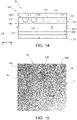
- the device layer 15 may comprise a drift layer and one or more implanted regions which may form, for example, source regions and body regions, depending on the specific application, examples whereof are shown for illustrative purposes in figure 14 .
- the device layer 15 may also comprise gate structures. In another embodiment, the device layer 15 may be a multilayer, with different device structures integrated in the various layers.
- connection structure layer 8 comprises one or more metal layers that form an electrical interconnect structure for the device layer 15.
- connection structure layer 8 may also comprise one or more layers of insulating materials, forming passivation structures.
- the device layer 15 and the connection structure layer 8 form at least one die portion, here a plurality of die portions 18.
- Each die portion 18 is intended to form a respective electronic device, after dicing the work body 1.
- Each die portion 18 has a die area, which occupies a respective portion of the area of the first surface 5A of the wafer 5.
- die portions 18 are schematically indicated by dashed lines.
- each die portion 18 has a rectangular shape in top plan view.
- the die area may be approximately of few millimeters squared, for example approximately 4 mm by 5 mm.
- the contact layer 20 is a metal material such as nickel, titanium or an alloy of nickel and silicon, and has a thickness, measured parallel to the third axis Z, comprised for example between 20 nm and 150 nm, in particular of about 100 nm.
- figure 4 the work body 1, in particular the contact layer 20, undergoes a laser annealing step.
- a laser source 30 is used to generate a light beam 33 and focus the light beam 33 on the contact surface 22.
- the light beam 33 has an energy density higher than 3 J/cm 2 , for example comprised between 3.4 J/cm 2 and 4.8 J/cm 2 , in particular of 4.0 J/cm 2 .
- the light beam 33 has a wavelength comprised, for example, between 290 nm and 370 nm, in particular of 310 nm.
- the light beam 33 may be a pulsed light beam having a duration comprised, for example, between 100 ns and 300 ns, in particular of 160 ns.
- the light beam 33 has a beam footprint 35 on the contact surface 22.
- Figures 5 and 6 show an energy profile of the beam footprint 35, parallel to the first axis X and, respectively, to the second axis Y.
- the beam footprint 35 has a first width W x parallel to the first axis X and comprises a first plateau region 36 having a first energy E max,x and a first plateau length L p,x , and two first sloped regions 37, each having a first slope length L s,x , wherein the beam energy decreases from the first energy E max,x to zero.
- the beam energy may decrease linearly in the first sloped regions 37, from the first energy E max,x to zero.
- the first energy E max,x is constant.
- the first width W x may be comprised, for example, between 8 mm and 36 mm, in particular may be about 10 mm.
- the first slope length L s,x is much smaller than the first plateau length L p,x .
- the first slope length L s,x is comprised between 0,5% and 5% of the first plateau length L p,x , in particular about 3% of the first plateau length L p,x .
- the first slope length L s,x may be comprised between 50 ⁇ m and 500 ⁇ m, in particular may be 300 ⁇ m.
- the first plateau length L p,x is about the same as the first width W x of the beam footprint 35.
- the beam footprint 35 has a second width Wy parallel to the second axis Y and comprises a second plateau region 38 having a second energy E max,Y and a second plateau length L p,Y , and two second sloped regions 39, each having a second slope length L s,Y , wherein the beam energy decreases from the second energy E max,Y to zero.
- the beam energy may decrease linearly in the second sloped regions 39, from the second energy E max,Y to zero.
- the second energy E max,Y is constant and equal to the first energy E max,X .
- the second width Wy may be comprised, for example, between 8 mm and 36 mm, in particular may be about 10 mm.
- the second slope length L s,Y is much smaller than the second plateau length L p,Y .
- the second slope length L s,Y is comprised between 0,5% and 5% of the second plateau length L p,Y , in particular about 3% of the second plateau length L p,Y .
- the second slope length L s,Y may be comprised between 50 ⁇ m and 500 ⁇ m, in particular may be 300 ⁇ m.
- the second plateau length L p,Y is about the same as the second width Wy of the beam footprint 35.
- the beam footprint 35 has the same energy profile as the ones shown in figures 5 and 6 for every section parallel to the first axis X and, respectively, to the second axis Y.
- the energy profile of the beam footprint 35 along any direction parallel to the first axis X is equal to the energy profile along any direction parallel to the second axis Y. Therefore, a 3-dimesional representation of the energy profile of the beam footprint 35 is a truncated pyramid, as shown in the perspective view of figure 7 .
- the footprint 35 may be obtained for example using the laser LT-3100 manufactured by SCREEN Semiconductor Solutions Co., Ltd.
- the beam footprint 35 forms a polygonal shape on the contact surface 22, in particular a squared shape, as shown in figure 8 , whose sides have the first width Wx along the first axis X and the second width Wy along the second axis Y.
- the beam footprint 35 forms a central region 42, which is irradiated with a constant energy and corresponds to the first plateau region 36 and the second plateau region 38, and a gradient region 44, which is irradiated with a non-constant energy and corresponds to the first sloped regions 37 and the second sloped regions 39, wherein the gradient region 44 surrounds the central region 42.
- the laser source 30 focuses the laser beam 33 on a first portion 47 of the contact surface 22 ( figure 9 ).
- the laser beam 33 is absorbed by the contact layer 20 and by part of the work substrate 12.
- the absorbed light generates heat locally, i.e. immediately under the first portion 47 of the contact surface 22, for example to a depth of few microns from the contact surface 22.
- the generated heat makes the contact layer 20 and the work substrate 12 to react locally, at a respective portion of the second surface 5B of the wafer 5, forming a silicide, for example nickel silicide or titanium silicide.
- a silicide for example nickel silicide or titanium silicide.
- the contact surface 22 is scanned using a step-and-repeat approach.
- the work body 1 is moved with respect to the laser beam 33 so that the laser beam 33 is focused on a second portion 48 of the contact surface 22 ( figure 9 ).
- the second portion 48 of the contact surface 22 partially overlaps the first portion 47 of the contact surface 22 and partially extends next to the first portion 47 of the contact surface 22 along a first scanning line A parallel to the first axis X.
- the relative movement of the work body 1 with respect to the laser source 30 causes the beam footprint 35 to move by a first shift step D X along the first scanning line A. Therefore, also the second portion 48 of the contact surface 22 is shifted with respect to the first portion 47 of the contact surface 22 along the first scanning line A, on the right in figure 9 , by the first shift step Dx.
- the first shift step D X is smaller than the first width W X of the beam footprint 35.
- the first shift step Dx is a fraction of the first width W X , for example comprised between one tenth and one half of the first width Wx, in particular about one fourth of the first width W X .
- the first width Wx may be 10 mm and the first shift step D X may be smaller than 2.5 mm.
- the laser source 30 focuses the laser beam 33 on subsequent portions of the contact surface 22 along the first scanning line A throughout the entire length of the contact surface 22 along the first scanning line A.
- the laser beam 33 scans the contact surface 22 along a second scanning line, here not shown, parallel to the first scanning line A and shifted along the second axis Y to expose a third portion 49 of the contact surface 22, as shown for example in figure 10 , where the third portion 49 of the contact surface 22, for clarity, is drawn with a dashed line.
- the third portion 49 of the contact surface 22 partially overlaps the first portion 47 of the contact surface 22 and partially extends next to the first portion 47 of the contact surface 22 along a direction parallel to the second axis Y.
- the relative movement of the work body 1 with respect to the laser source 30 causes the beam footprint to move by a second shift step Dy in a direction parallel to the second axis Y with respect to the position of the first portion 47. Therefore, the third portion 49 of the contact surface 22 is shifted by the second shift step Dy, parallel to the second axis Y, from the first portion 47.
- the second shift step Dy is smaller than the second width W Y .
- the second shift step Dy is a fraction of the second width Wy, for example comprised between one tenth and one half of the second width Wy, in particular about one fourth of the second width Wy.
- the second width Wy may be 10 mm and the second shift step Dy may be smaller than 2.5 mm.
- the entire contact surface 22 is scanned by the laser beam 33.
- adjacent irradiated portions of the contact surface 22 may be shifted by steps different from the first shift step D X and the second shift step Dy.
- the first shift step Dx may be different from the second shift step Dy.
- first shift step Dx or the second shift step D Y may be varied along a same scan line or among different scan lines. This may allow to tune the distance between adjacent gradient regions 44, for example to increase (or decrease) the density of gradient regions 44 in specific portions of the contact surface 22.
- Figure 11 shows the work body 1 after the contact surface 22 has been completely exposed by the laser beam 33, thereby causing the complete reaction of the contact layer 20 with the work substrate 12 and formation of an ohmic layer 50.
- the ohmic layer 50 is of silicide and extends between a first surface 50A, which corresponds to the second surface 5B of the wafer 5, and a second surface 50B, which corresponds to the contact surface 22.
- the ohmic layer 50 is thicker than the contact layer 20, since also part of the work substrate 12 has reacted to form the ohmic layer 50.
- Figure 12 shows a top plan view of the second surface 50B of the ohmic layer 50, according to an idealized representation.
- the ohmic layer 50 comprises a rough region 55 and a plurality of smooth regions 57.
- the smooth regions 57 correspond to the portions of the contact surface 22 that have been exposed only to the first plateau region 36 and the second plateau region 38 of the beam footprint 35, i.e. that have received a spatially uniform energy.
- the rough region 55 corresponds to the gradient portions 44 of the contact surface 22, i.e. to the portions of the contact surface 22 that have received a spatially non-uniform energy.
- the gradient of energy of the gradient regions 44 generates in fact also a thermal gradient during the laser annealing step of figure 4 , which in turn causes the rough region to have an increased roughness with respect to the smooth regions 57, as also discussed below with reference to figure 15 .
- the rough region 55 is a grid formed by a plurality of horizontal stripes 58, parallel to the first axis X, and a plurality of vertical stripes 59, parallel to the second axis Y.
- Each horizontal stripe 58 has a width Lx, parallel to the first axis X, which approximately corresponds to the first slope length L s,X of the beam footprint 35 and extends at a distance from an adjacent horizontal stripe 58 that is approximately equal to the first shift step Dx.
- Each vertical stripe 59 has a width Ly, parallel to the second axis Y, which approximately corresponds to the second slope length L s,Y of the beam footprint 35 and extends at a distance from an adjacent vertical stripe 59 that is approximately equal to the second shift step Dy.
- the number of horizontal stripes 58 and vertical stripes 59 may be changed.
- the first shift step D X and the second shift step Dy have been chosen so that each die portion 18 has two horizontal stripes 58 and two vertical stripes 59.
- a metallization layer 60 is deposited on the second surface 50B of the ohmic layer 50.
- the metallization layer 60 may be a single metal layer or a stack of different metal layers, for example Ti/NiV/Ag.
- the metallization layer 60 is useful for subsequent manufacturing steps, for example assembling processes such as sintering and diffusion soldering.
- the work body 1 is then subject to known final manufacturing steps, such as dicing, thereby forming an electronic device 100 ( figure 14 ) for each die portion 18.
- the electronic device 100 comprises a die 103 including a body 105 having a first surface 105A, which corresponds to the first surface 5A of the wafer 5, and a second surface 105B, which corresponds to the first surface 50A of the ohmic layer 50.
- the body 105 comprises a substrate 107 (corresponding to the work substrate 12 and forming the second surface 105B) and a device region 109 (corresponding to the device layer 15 and forming the first surface 105A).
- the device region 109 accommodates functional regions of various kind and dimensions, according to the specific type of the electronic device 100 and the specific application.
- the electronic device 100 may be a JBS or an MPS diode.
- the device region 109 forms a drift region 111 of a first conductivity type, e.g. N-type, accommodating two implanted regions 113 of a second conductivity type, e.g. P-type.
- the electronic device 100 may be a MOSFET device.
- the drift region 111 accommodates body regions 115 of the second conductivity type, source regions 117 of the first conductivity type and insulated gate regions 120 of dielectric material (represented with dashed lines in figure 14 ).
- the die 103 comprises an ohmic connection region 123, corresponding to the ohmic layer 50, extending on the second surface 105B of the body 105 and forming a metallization contact surface, which corresponds to the second surface 50B of the ohmic layer 50 and therefore it is indicated by the same reference number.
- the die 103 also comprises a back metallization region 125 corresponding to the metallization layer 60 and extending on the metallization contact surface 50B.
- the die 103 further comprises a connection structure region 127 corresponding to the connection structure layer 8, extending on the first surface 105A of the body 105.
- the device region 109 and the connection structure region 127 correspond to a respective die portion 18 ( figure 2 ).
- the electronic device 100 has a current path 128, schematically represented by a dashed arrow in figure 14 , which extends between the connection structure region 111 and the back metallization region 125, through the body 105.
- a current may flow through the current path 128, depending on the specific structure of the device region 109, i.e. on the type of the electronic device 100.
- the ohmic connection region 123 shows a high mechanical stability.
- the ohmic connection region 123 comprises a rough region and one or more smooth regions.
- the rough region and the smooth regions correspond to the portion of the rough region 55 and, respectively, to the smooth regions 57 within the respective die portion 18 of figure 12 . Therefore, hereinafter, the rough region of the ohmic connection region 123 is indicated by the same reference number as the rough region 55 of figure 12 and the smooth regions of the ohmic connection region 123 are indicated by the same reference number as the smooth regions 57 of figure 12 .
- the shape of the rough region 55 of the ohmic connection region 123 depends on the first and the second shift step Dx, Dy, and on the first width W X , the second width Wy, the first slope length L s,X and the second slope length L s,Y of the beam footprint 35. Accordingly, the rough region 55 of the ohmic connection region 123 is formed by portions of the horizontal stripes 58 and portions of the vertical stripes 59.
- the rough region 55 of the ohmic connection region 123 is formed by portions of two adjacent horizontal stripes 58 and portions of two adjacent vertical stripes 59.
- the percentage of the ohmic connection region 123 that is formed by the smooth regions 57 (and accordingly by the rough region 55) may be varied.
- the rough region 55 of the ohmic connection region 123 has a non-uniform thickness along the third axis Z.
- the rough region 55 of the ohmic connection region 123 has, at the second surface 105B of the body 105 and at the second surface 50B of the ohmic connection region 123, a higher roughness than the smooth regions 57 of the ohmic connection region 123.
- Figure 15 is an exemplificative zoomed-in micrograph of a portion of the second surface 50B of the ohmic connection region 123, showing the effect of the gradient regions 44 during the laser annealing of figure 4 .
- the micrograph of figure 15 shows a portion 130 of the rough region 55 of the ohmic connection region and two portions 135 of the smooth region 57.
- the portion 130 of the rough region 55 which corresponds for example to a portion of an horizontal stripe 58 or of a vertical stripe 59, is formed by a plurality of protrusions 140 of silicide, each having a diameter comprised for example between 0.5 ⁇ m and 2 ⁇ m.
- the Applicant has verified that the protrusions 140 increase the mechanical robustness of the ohmic connection region 123.
- the electronic device 100 is therefore less subject to mechanical defects such as fracture and delamination of the ohmic connection region 123.
- a shear test of the electronic device 100 shows an average increase of the shear strength of the electronic device 100 even up to 156% with respect to a case wherein the electronic device 100 has no overlap portions.
- the ohmic connection region 123 ensures a good electrical contact, in particular an ohmic contact, with the substrate 107. Therefore, the electronic device 100 also maintains good electrical properties.
- the beam footprint 35 may have a different shape such as rectangular, circular or any other shape.
- the energy profile along the first axis may be different from the energy profile along the second axis Y.
- the spatial trend of the first and the second sloped regions 37, 39 may be different, such as non-linear.
- a higher number of laser shots or pulses may be used to expose each irradiated portion of the contact surface 22. For example, two to five laser shots or pulses may be used.
- the step-and-repeat type of scanning may be achieved either by moving the work body 1, by moving the laser source 30, by deflecting the laser beam 33 or a combination thereof, depending on the specific application.
- the shape of the rough region 55 of figure 12 (and accordingly also of the rough region 55 of the ohmic connection layer 123 of the electronic device 100) may be different.
- a different number of horizontal and vertical stripes 58, 59 may be comprised in a die portion 18.
- the density of horizontal and vertical stripes 58, 59 may be so high that the ohmic layer 50 (and therefore also the ohmic connection region 123 of the electronic device 100) is approximately entirely formed by a rough region.
- the rough region 55 may have a shape different from a grid, for example the rough region 55 may form a non-regular pattern such as a plurality of separated portions with increased roughness.
Landscapes
- Electrodes Of Semiconductors (AREA)
- Carbon And Carbon Compounds (AREA)
- Crystals, And After-Treatments Of Crystals (AREA)
Abstract
Description
- The present invention is relative to a process for manufacturing a vertical conduction silicon carbide electronic device and to a vertical conduction silicon carbide electronic device.
- As known, silicon carbide (SiC) electronic devices such as Junction Barrier Schottky (JBS) diodes, Merged PiN Schottky (MPS) diodes and MOSFET transistors, have better performances than silicon electronic devices, in particular for power applications, wherein high operating voltages or other specific operating conditions, such as high temperature, are employed.
- A silicon carbide electronic device for power applications, hereinafter indicated as power device, comprises a silicon carbide body, a front metal region and a back metal region. In use, a current may flow through the silicon carbide body between the front metal region and the back metal region.
- It is known to obtain the power device from a silicon carbide wafer having a front surface and a back surface, in one of its polytypes, such as 3C-SiC, 4H-SiC and 6H-SiC.
- During initial manufacturing steps, devices like transistors, diodes, resistors, etc. are generally formed in the silicon carbide body from the front surface. Then, the front metal region is formed on the front surface to mutually interconnect the integrated devices as well as to allow connection of the power device with external circuit components and/or stages.
- In addition, the back surface of the wafer is processed, so as to form the back metal region.
- To this end, a metal layer, e.g. nickel or titanium, is deposited on the back surface.
- Then, a laser beam is used to heat the metal layer and cause the metal layer to fully react with the silicon carbide atoms of the wafer, thereby forming a silicide layer, e.g. titanium or nickel silicide.
- In detail, the used laser beam has a spot having an area that is much smaller than the area of the back surface of the wafer. Therefore, in order to entirely expose the back surface, a step-and-repeat approach is used, wherein a first laser shot exposes a first portion of the back surface, the laser beam (or the wafer) is moved, and a second laser shot exposes a second portion of the back surface.
- In order to maximize the throughput of the manufacturing process, it is known to move the laser beam so that the spots of adjacent laser shots have possibly no overlap on the back surface. In practice, the laser beam is moved, between two consecutive shots, by a quantity that is approximately equal to the size of the spot.
- Subsequently, a metallization layer is deposited on the silicide layer.
- After final manufacturing steps including dicing, the power device is obtained.
- The Applicant has verified that, in some cases, the silicide layer of such known power devices has a low mechanical stability. In fact, during some reliability tests, it has been observed that the silicide layer has a high probability of delamination from the silicon carbide body or mechanical fracture, thereby causing failure of the power device.
- The aim of the present invention is to overcome the disadvantages of the prior art.
- According to the present invention, a process for manufacturing a vertical conduction silicon carbide electronic device and a vertical conduction silicon carbide electronic device are provided, as defined in the attached claims.
- For a better understanding of the present invention, a non-limiting embodiment is now described, with reference to the attached drawings, wherein:
-
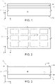
figure 1 shows a cross-section of a work body comprising a silicon carbide wafer, according to the present manufacturing process; -
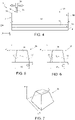
figure 2 is a top plan view of the work body offigure 1 ; -
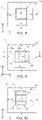
figure 3 is a cross-section of the work body offigure 1 in a subsequent manufacturing step; -
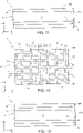
figure 4 is a cross-section of the work body offigure 3 in a subsequent manufacturing step comprising a laser annealing step; -
figures 5 and 6 show an energy profile of a footprint of a laser beam along two different directions; -
figure 7 shows a perspective view of the energy profile of the footprint offigures 5 and 6 ; -
figure 8 shows a top-plan view of the footprint of the laser beam offigures 5-7 formed on the work body, during the laser annealing step offigure 4 ; -
figures 9 and 10 are schematic representations of a scanning method of the laser annealing step offigure 4 ; -
figures 11 and 12 are respectively a cross-section and a top plan view of the work body offigure 4 after the laser annealing step; -
figure 13 shows a cross-section of the work body offigures 11 and 12 in a subsequent manufacturing step; -
figure 14 is a cross-section of the present electronic device; and -
figure 15 is an exemplificative micrograph of a surface of the present electronic device. -
Figures 1 and 2 show awork body 1 in a Cartesian reference system XYZ comprising a first axis X, a second axis Y and a third axis Z. - The
work body 1 has already been subject to first manufacturing steps. - The
work body 1 is formed by awafer 5 of silicon carbide (SiC) in one of its polytypes, such as 3C-SiC, 4H-SiC and 6H-SiC, having afirst surface 5A and asecond surface 5B, and by aconnection structure layer 8 extending on thefirst surface 5A of thewafer 5. - The
wafer 5 comprises awork substrate 12, which forms thesecond surface 5B of thewafer 5, and adevice layer 15, which forms thefirst surface 5A of thewafer 5 and extends directly on thework substrate 12. - The
device layer 15 may be a portion of thework substrate 12 or may be an epitaxial layer grown on thework substrate 12. - The
device layer 15 comprises current conduction zones, here not shown, whose structure, number and configuration depend on the specific application. - For example, the
device layer 15 may comprise a drift layer and one or more implanted regions which may form, for example, source regions and body regions, depending on the specific application, examples whereof are shown for illustrative purposes infigure 14 . - In an embodiment, the
device layer 15 may also comprise gate structures. In another embodiment, thedevice layer 15 may be a multilayer, with different device structures integrated in the various layers. - The
connection structure layer 8 comprises one or more metal layers that form an electrical interconnect structure for thedevice layer 15. - According to an embodiment, the
connection structure layer 8 may also comprise one or more layers of insulating materials, forming passivation structures. - The
device layer 15 and theconnection structure layer 8 form at least one die portion, here a plurality of dieportions 18. - Each
die portion 18 is intended to form a respective electronic device, after dicing thework body 1. - Each
die portion 18 has a die area, which occupies a respective portion of the area of thefirst surface 5A of thewafer 5. - In
figure 2 , for simplicity, the dieportions 18 are schematically indicated by dashed lines. - In detail, in this embodiment, each
die portion 18 has a rectangular shape in top plan view. By way of example only, the die area may be approximately of few millimeters squared, for example approximately 4 mm by 5 mm. - Subsequently,
figure 3 , thework body 1 is flipped upside down and acontact layer 20 is deposited on thesecond surface 5B of thewafer 5, forming acontact surface 22 of thework body 1. - The
contact layer 20 is a metal material such as nickel, titanium or an alloy of nickel and silicon, and has a thickness, measured parallel to the third axis Z, comprised for example between 20 nm and 150 nm, in particular of about 100 nm. - Then,
figure 4 , thework body 1, in particular thecontact layer 20, undergoes a laser annealing step. - In detail, a
laser source 30 is used to generate alight beam 33 and focus thelight beam 33 on thecontact surface 22. - The
light beam 33 has an energy density higher than 3 J/cm2, for example comprised between 3.4 J/cm2 and 4.8 J/cm2, in particular of 4.0 J/cm2. - The
light beam 33 has a wavelength comprised, for example, between 290 nm and 370 nm, in particular of 310 nm. - The
light beam 33 may be a pulsed light beam having a duration comprised, for example, between 100 ns and 300 ns, in particular of 160 ns. - The
light beam 33 has abeam footprint 35 on thecontact surface 22. -
Figures 5 and 6 show an energy profile of thebeam footprint 35, parallel to the first axis X and, respectively, to the second axis Y. - In detail (
figure 5 ), thebeam footprint 35 has a first width Wx parallel to the first axis X and comprises afirst plateau region 36 having a first energy Emax,x and a first plateau length Lp,x, and two first slopedregions 37, each having a first slope length Ls,x, wherein the beam energy decreases from the first energy Emax,x to zero. - In particular, the beam energy may decrease linearly in the first sloped
regions 37, from the first energy Emax,x to zero. - Moreover, in this embodiment, the first energy Emax,x is constant.
- The first width Wx may be comprised, for example, between 8 mm and 36 mm, in particular may be about 10 mm.
- In this embodiment, the first slope length Ls,x is much smaller than the first plateau length Lp,x. For example, the first slope length Ls,x is comprised between 0,5% and 5% of the first plateau length Lp,x, in particular about 3% of the first plateau length Lp,x.
- For example, the first slope length Ls,x may be comprised between 50 µm and 500 µm, in particular may be 300 µm.
- Accordingly, in a first approximation, the first plateau length Lp,x is about the same as the first width Wx of the
beam footprint 35. - In addition (
figure 6 ), thebeam footprint 35 has a second width Wy parallel to the second axis Y and comprises asecond plateau region 38 having a second energy Emax,Y and a second plateau length Lp,Y, and two secondsloped regions 39, each having a second slope length Ls,Y, wherein the beam energy decreases from the second energy Emax,Y to zero. - In particular, here, the beam energy may decrease linearly in the second
sloped regions 39, from the second energy Emax,Y to zero. - Moreover, in this embodiment, the second energy Emax,Y is constant and equal to the first energy Emax,X.
- The second width Wy may be comprised, for example, between 8 mm and 36 mm, in particular may be about 10 mm.
- In this embodiment, also the second slope length Ls,Y is much smaller than the second plateau length Lp,Y. For example, the second slope length Ls,Y is comprised between 0,5% and 5% of the second plateau length Lp,Y, in particular about 3% of the second plateau length Lp,Y.
- For example, the second slope length Ls,Y may be comprised between 50 µm and 500 µm, in particular may be 300 µm.
- Accordingly, in a first approximation, the second plateau length Lp,Y is about the same as the second width Wy of the
beam footprint 35. - In this embodiment, the
beam footprint 35 has the same energy profile as the ones shown infigures 5 and 6 for every section parallel to the first axis X and, respectively, to the second axis Y. - Moreover, in this embodiment, the energy profile of the
beam footprint 35 along any direction parallel to the first axis X is equal to the energy profile along any direction parallel to the second axis Y. Therefore, a 3-dimesional representation of the energy profile of thebeam footprint 35 is a truncated pyramid, as shown in the perspective view offigure 7 . - The
footprint 35 may be obtained for example using the laser LT-3100 manufactured by SCREEN Semiconductor Solutions Co., Ltd. - The
beam footprint 35 forms a polygonal shape on thecontact surface 22, in particular a squared shape, as shown infigure 8 , whose sides have the first width Wx along the first axis X and the second width Wy along the second axis Y. - In practice, for each portion of the
contact surface 22 that is exposed by thelaser beam 33, thebeam footprint 35 forms acentral region 42, which is irradiated with a constant energy and corresponds to thefirst plateau region 36 and thesecond plateau region 38, and agradient region 44, which is irradiated with a non-constant energy and corresponds to the firstsloped regions 37 and the secondsloped regions 39, wherein thegradient region 44 surrounds thecentral region 42. - In
figures 8-10 , for clarity, thegradient region 44 is indicated with oblique lines. - During the annealing step of
figure 4 , thelaser source 30 focuses thelaser beam 33 on afirst portion 47 of the contact surface 22 (figure 9 ). - The
laser beam 33 is absorbed by thecontact layer 20 and by part of thework substrate 12. The absorbed light generates heat locally, i.e. immediately under thefirst portion 47 of thecontact surface 22, for example to a depth of few microns from thecontact surface 22. - The generated heat makes the
contact layer 20 and thework substrate 12 to react locally, at a respective portion of thesecond surface 5B of thewafer 5, forming a silicide, for example nickel silicide or titanium silicide. - In order to cause the reaction of the
entire contact layer 20 with thework substrate 12, thecontact surface 22 is scanned using a step-and-repeat approach. - In detail, the
work body 1 is moved with respect to thelaser beam 33 so that thelaser beam 33 is focused on asecond portion 48 of the contact surface 22 (figure 9 ). - For clarity, in
figure 9 , thesecond portion 48 of thecontact surface 22 is drawn by a dashed line. - The
second portion 48 of thecontact surface 22 partially overlaps thefirst portion 47 of thecontact surface 22 and partially extends next to thefirst portion 47 of thecontact surface 22 along a first scanning line A parallel to the first axis X. - In detail, the relative movement of the
work body 1 with respect to thelaser source 30 causes thebeam footprint 35 to move by a first shift step DX along the first scanning line A. Therefore, also thesecond portion 48 of thecontact surface 22 is shifted with respect to thefirst portion 47 of thecontact surface 22 along the first scanning line A, on the right infigure 9 , by the first shift step Dx. - The first shift step DX is smaller than the first width WX of the
beam footprint 35. - In detail, the first shift step Dx is a fraction of the first width WX, for example comprised between one tenth and one half of the first width Wx, in particular about one fourth of the first width WX.
- For example, in one embodiment, the first width Wx may be 10 mm and the first shift step DX may be smaller than 2.5 mm.
- Subsequently, the
laser source 30 focuses thelaser beam 33 on subsequent portions of thecontact surface 22 along the first scanning line A throughout the entire length of thecontact surface 22 along the first scanning line A. - Subsequently, the
laser beam 33 scans thecontact surface 22 along a second scanning line, here not shown, parallel to the first scanning line A and shifted along the second axis Y to expose athird portion 49 of thecontact surface 22, as shown for example infigure 10 , where thethird portion 49 of thecontact surface 22, for clarity, is drawn with a dashed line. - The
third portion 49 of thecontact surface 22 partially overlaps thefirst portion 47 of thecontact surface 22 and partially extends next to thefirst portion 47 of thecontact surface 22 along a direction parallel to the second axis Y. - In detail, the relative movement of the
work body 1 with respect to thelaser source 30 causes the beam footprint to move by a second shift step Dy in a direction parallel to the second axis Y with respect to the position of thefirst portion 47. Therefore, thethird portion 49 of thecontact surface 22 is shifted by the second shift step Dy, parallel to the second axis Y, from thefirst portion 47. - The second shift step Dy is smaller than the second width WY. In detail, the second shift step Dy is a fraction of the second width Wy, for example comprised between one tenth and one half of the second width Wy, in particular about one fourth of the second width Wy.
- For example, in one embodiment, the second width Wy may be 10 mm and the second shift step Dy may be smaller than 2.5 mm.
- By repeating the steps discussed above, the
entire contact surface 22 is scanned by thelaser beam 33. - In general, adjacent irradiated portions of the
contact surface 22 may be shifted by steps different from the first shift step DX and the second shift step Dy. - For example, the first shift step Dx may be different from the second shift step Dy.
- In addition, the first shift step Dx or the second shift step DY may be varied along a same scan line or among different scan lines. This may allow to tune the distance between
adjacent gradient regions 44, for example to increase (or decrease) the density ofgradient regions 44 in specific portions of thecontact surface 22. -
Figure 11 shows thework body 1 after thecontact surface 22 has been completely exposed by thelaser beam 33, thereby causing the complete reaction of thecontact layer 20 with thework substrate 12 and formation of anohmic layer 50. - The
ohmic layer 50 is of silicide and extends between afirst surface 50A, which corresponds to thesecond surface 5B of thewafer 5, and asecond surface 50B, which corresponds to thecontact surface 22. - Generally, the
ohmic layer 50 is thicker than thecontact layer 20, since also part of thework substrate 12 has reacted to form theohmic layer 50. -
Figure 12 shows a top plan view of thesecond surface 50B of theohmic layer 50, according to an idealized representation. By virtue of the laser annealing step offigure 4 , theohmic layer 50 comprises arough region 55 and a plurality ofsmooth regions 57. - The
smooth regions 57 correspond to the portions of thecontact surface 22 that have been exposed only to thefirst plateau region 36 and thesecond plateau region 38 of thebeam footprint 35, i.e. that have received a spatially uniform energy. - The
rough region 55 corresponds to thegradient portions 44 of thecontact surface 22, i.e. to the portions of thecontact surface 22 that have received a spatially non-uniform energy. - The gradient of energy of the
gradient regions 44 generates in fact also a thermal gradient during the laser annealing step offigure 4 , which in turn causes the rough region to have an increased roughness with respect to thesmooth regions 57, as also discussed below with reference tofigure 15 . - Again with reference to
figure 12 , in this embodiment, therough region 55 is a grid formed by a plurality ofhorizontal stripes 58, parallel to the first axis X, and a plurality ofvertical stripes 59, parallel to the second axis Y. - Each
horizontal stripe 58 has a width Lx, parallel to the first axis X, which approximately corresponds to the first slope length Ls,X of thebeam footprint 35 and extends at a distance from an adjacenthorizontal stripe 58 that is approximately equal to the first shift step Dx. - Each
vertical stripe 59 has a width Ly, parallel to the second axis Y, which approximately corresponds to the second slope length Ls,Y of thebeam footprint 35 and extends at a distance from an adjacentvertical stripe 59 that is approximately equal to the second shift step Dy. - By changing the first shift step Dx and the second shift step Dy, the number of
horizontal stripes 58 andvertical stripes 59 may be changed. - In this embodiment, as visible in
figure 12 , the first shift step DX and the second shift step Dy have been chosen so that each dieportion 18 has twohorizontal stripes 58 and twovertical stripes 59. - In
figure 13 , ametallization layer 60 is deposited on thesecond surface 50B of theohmic layer 50. Themetallization layer 60 may be a single metal layer or a stack of different metal layers, for example Ti/NiV/Ag. - The
metallization layer 60 is useful for subsequent manufacturing steps, for example assembling processes such as sintering and diffusion soldering. - The
work body 1 is then subject to known final manufacturing steps, such as dicing, thereby forming an electronic device 100 (figure 14 ) for each dieportion 18. - The
electronic device 100 comprises a die 103 including abody 105 having afirst surface 105A, which corresponds to thefirst surface 5A of thewafer 5, and asecond surface 105B, which corresponds to thefirst surface 50A of theohmic layer 50. - The
body 105 comprises a substrate 107 (corresponding to thework substrate 12 and forming thesecond surface 105B) and a device region 109 (corresponding to thedevice layer 15 and forming thefirst surface 105A). - The
device region 109, as discussed above for thedevice layer 15, accommodates functional regions of various kind and dimensions, according to the specific type of theelectronic device 100 and the specific application. - By way of example, the
electronic device 100 may be a JBS or an MPS diode. In this case, as shown infigure 14 by way of example, thedevice region 109 forms adrift region 111 of a first conductivity type, e.g. N-type, accommodating two implantedregions 113 of a second conductivity type, e.g. P-type. - As an alternative, as also shown as an example in
figure 14 , theelectronic device 100 may be a MOSFET device. In this case, thedrift region 111 accommodatesbody regions 115 of the second conductivity type,source regions 117 of the first conductivity type andinsulated gate regions 120 of dielectric material (represented with dashed lines infigure 14 ). - The
die 103 comprises anohmic connection region 123, corresponding to theohmic layer 50, extending on thesecond surface 105B of thebody 105 and forming a metallization contact surface, which corresponds to thesecond surface 50B of theohmic layer 50 and therefore it is indicated by the same reference number. - The
die 103 also comprises aback metallization region 125 corresponding to themetallization layer 60 and extending on themetallization contact surface 50B. - The die 103 further comprises a
connection structure region 127 corresponding to theconnection structure layer 8, extending on thefirst surface 105A of thebody 105. - In detail, the
device region 109 and theconnection structure region 127 correspond to a respective die portion 18 (figure 2 ). - In use, the
electronic device 100 has acurrent path 128, schematically represented by a dashed arrow infigure 14 , which extends between theconnection structure region 111 and theback metallization region 125, through thebody 105. - In use, a current may flow through the
current path 128, depending on the specific structure of thedevice region 109, i.e. on the type of theelectronic device 100. - The
ohmic connection region 123 shows a high mechanical stability. - The
ohmic connection region 123 comprises a rough region and one or more smooth regions. The rough region and the smooth regions correspond to the portion of therough region 55 and, respectively, to thesmooth regions 57 within therespective die portion 18 offigure 12 . Therefore, hereinafter, the rough region of theohmic connection region 123 is indicated by the same reference number as therough region 55 offigure 12 and the smooth regions of theohmic connection region 123 are indicated by the same reference number as thesmooth regions 57 offigure 12 . - The shape of the
rough region 55 of theohmic connection region 123 depends on the first and the second shift step Dx, Dy, and on the first width WX, the second width Wy, the first slope length Ls,X and the second slope length Ls,Y of thebeam footprint 35. Accordingly, therough region 55 of theohmic connection region 123 is formed by portions of thehorizontal stripes 58 and portions of thevertical stripes 59. - In detail, in this embodiment, the
rough region 55 of theohmic connection region 123 is formed by portions of two adjacenthorizontal stripes 58 and portions of two adjacentvertical stripes 59. - Depending on the first and the second shift step DX, Dy, and on the first width WX, the second width WY, the first slope length Ls,X and the second slope length Ls,Y of the
beam footprint 35, the percentage of theohmic connection region 123 that is formed by the smooth regions 57 (and accordingly by the rough region 55) may be varied. - The
rough region 55 of theohmic connection region 123 has a non-uniform thickness along the third axis Z. - The
rough region 55 of theohmic connection region 123 has, at thesecond surface 105B of thebody 105 and at thesecond surface 50B of theohmic connection region 123, a higher roughness than thesmooth regions 57 of theohmic connection region 123. -
Figure 15 is an exemplificative zoomed-in micrograph of a portion of thesecond surface 50B of theohmic connection region 123, showing the effect of thegradient regions 44 during the laser annealing offigure 4 . - The micrograph of
figure 15 shows aportion 130 of therough region 55 of the ohmic connection region and twoportions 135 of thesmooth region 57. Theportion 130 of therough region 55, which corresponds for example to a portion of anhorizontal stripe 58 or of avertical stripe 59, is formed by a plurality ofprotrusions 140 of silicide, each having a diameter comprised for example between 0.5 µm and 2 µm. - The Applicant has verified that the
protrusions 140 increase the mechanical robustness of theohmic connection region 123. Theelectronic device 100 is therefore less subject to mechanical defects such as fracture and delamination of theohmic connection region 123. - In particular, a shear test of the
electronic device 100, performed by the Applicant after subjecting test devices to one hundred thermal cycles, shows an average increase of the shear strength of theelectronic device 100 even up to 156% with respect to a case wherein theelectronic device 100 has no overlap portions. - At the same time, the
ohmic connection region 123 ensures a good electrical contact, in particular an ohmic contact, with thesubstrate 107. Therefore, theelectronic device 100 also maintains good electrical properties. - It is clear that the present manufacturing method and the corresponding electronic device may be subject to modifications and variations without departing the scope of the present invention, as defined in the attached claims.
- For example, the
beam footprint 35 may have a different shape such as rectangular, circular or any other shape. - In addition, the energy profile along the first axis may be different from the energy profile along the second axis Y. For example, the spatial trend of the first and the second
sloped regions - Moreover, a higher number of laser shots or pulses may be used to expose each irradiated portion of the
contact surface 22. For example, two to five laser shots or pulses may be used. - In the annealing step of
figure 4 , the step-and-repeat type of scanning may be achieved either by moving thework body 1, by moving thelaser source 30, by deflecting thelaser beam 33 or a combination thereof, depending on the specific application. - Moreover, the shape of the
rough region 55 offigure 12 (and accordingly also of therough region 55 of theohmic connection layer 123 of the electronic device 100) may be different. A different number of horizontal andvertical stripes die portion 18. For example, the density of horizontal andvertical stripes ohmic connection region 123 of the electronic device 100) is approximately entirely formed by a rough region. - Alternatively, the
rough region 55 may have a shape different from a grid, for example therough region 55 may form a non-regular pattern such as a plurality of separated portions with increased roughness.
Claims (16)
- A process for manufacturing a vertical conduction silicon carbide electronic device, the process comprising:- depositing, on a wafer (5) comprising silicon carbide, a metal layer (20), the metal layer forming a contact face (22); and- laser annealing the contact face (22) with a laser beam (33), the laser beam having a footprint (35) having a size (Lp,X, Lp,Y, WX, WY), thereby causing the metal layer to react with the wafer, forming a silicide layer (50);wherein laser annealing the contact face comprises irradiating a first portion (47) of the contact face, moving the footprint (35) of the laser beam by a step (DX, Dy) smaller than the size of the footprint and irradiating a second portion (48, 49) of the contact face, thereby causing the first portion and the second portion of the contact face to overlap, wherein the footprint (35) forms, on the contact face (22), a gradient region (37, 39, 42) having a spatially varying energy, wherein the gradient region causes the formation of a rough region (55, 58, 59) of the silicide layer (50) .
- The process according to the preceding claim, wherein the rough region comprises a plurality of irregularly arranged protrusions (140) having a diameter in the range 0.5 µm-2 µm.
- The process according to claim 1 or 2, wherein the gradient region has a size (Ls,X, Ls,Y ) smaller than the size (Lp,X, Lp,Y, WX, Wy) of the footprint (35) .
- The process according to the preceding claim, wherein the size (Ls,X, Ls,Y ) of the gradient region (37, 39, 42) is comprised between 0.5% and 5% of the size (Lp,X, Lp,Y, WX, WY) of the footprint (35) .
- The process according to any of the preceding claims, wherein the step (DX, DY) is comprised between one tenth and one half of the size (Lp,X, Lp,Y, WX, WY) of the footprint (35) .
- The process according to any of the preceding claims, wherein the footprint (35) has a polygonal shape having a side comprised between 8 mm and 36 mm.
- The process according to any of the preceding claims, wherein the laser beam has an energy density comprised between 3.4 J/cm2 and 4.8 J/cm2.
- The process according to any of the preceding claims, wherein the laser beam is a pulsed beam having a duration comprised between 100 ns and 300 ns.
- The process according to any of the preceding claims, wherein the laser beam has a wavelength comprised between 290 nm and 370 nm.
- The process according to any of the preceding claims, wherein laser annealing comprises scanning the entire contact face (22) with the laser beam (33) using a step-and-repeat type of scanning.
- The process according to any of the preceding claims, further comprising depositing a metallization layer (60) on the silicide layer.
- The process according to any of the preceding claims, wherein the silicide layer is formed on a first conduction terminal surface (5B) of the wafer, the wafer also having a second conduction terminal surface (5A) and comprising a device layer (15) that forms the second conduction terminal surface, the process further comprising forming electrically conductive device regions (113, 115, 117) in the device layer, and forming a connection structure layer (8) on the second conduction terminal surface.
- A vertical conduction silicon carbide electronic device formed in a die (103) comprising:- a body (105) of silicon carbide; and- a contact region (123) of silicide extending on the body and forming a connection surface (50B),wherein the contact region comprises a first rough portion (58, 59, 130) and a second rough portion (58, 59, 130), the first rough portion extending at a distance from the second rough portion, the first rough portion and the second rough portion including a plurality of irregularly arranged protrusions (140) of silicide.
- The device according to the preceding claim, wherein the first rough portion and the second rough portion each have a width comprised between 50 µm and 500 µm, and wherein the distance between the first rough portion and the second rough portion is smaller than 2.5 mm.
- The device according to claim 13 or 14, wherein each protrusion has a diameter comprised between 0.5 µm and 2 µm.
- The device according to any of claims 13-15, wherein the contact region extends on a first conduction terminal surface (105B) of the body and the body (105) also has a second conduction terminal surface (105A), the device further comprising a device region (109) extending in the body and forming the second conduction terminal surface, and a connection structure region (111) extending on the second conduction terminal surface.
Applications Claiming Priority (1)
| Application Number | Priority Date | Filing Date | Title |
|---|---|---|---|
| IT102021000017060A IT202100017060A1 (en) | 2021-06-29 | 2021-06-29 | MANUFACTURING PROCEDURE OF A VERTICALLY CONDUCTED SILICON CARBIDE ELECTRONIC DEVICE AND VERTICALLY CONDUCTED SILICON CARBIDE ELECTRONIC DEVICE |
Publications (1)
| Publication Number | Publication Date |
|---|---|
| EP4113581A1 true EP4113581A1 (en) | 2023-01-04 |
Family
ID=77802116
Family Applications (1)
| Application Number | Title | Priority Date | Filing Date |
|---|---|---|---|
| EP22181471.8A Pending EP4113581A1 (en) | 2021-06-29 | 2022-06-28 | Process for manufacturing a vertical conduction silicon carbide electronic device and vertical conduction silicon carbide electronic device |
Country Status (3)
| Country | Link |
|---|---|
| US (1) | US20220415655A1 (en) |
| EP (1) | EP4113581A1 (en) |
| IT (1) | IT202100017060A1 (en) |
Families Citing this family (1)
| Publication number | Priority date | Publication date | Assignee | Title |
|---|---|---|---|---|
| IT202100027101A1 (en) | 2021-10-21 | 2023-04-21 | St Microelectronics Srl | PROCEDURE FOR MANUFACTURING A SILICON CARBIDE ELECTRONIC DEVICE AND SILICON CARBIDE ELECTRONIC DEVICE |
Citations (4)
| Publication number | Priority date | Publication date | Assignee | Title |
|---|---|---|---|---|
| RU188684U1 (en) * | 2019-01-10 | 2019-04-22 | Закрытое акционерное общество "ГРУППА КРЕМНИЙ ЭЛ" | POWER SEMICONDUCTOR DEVICE BASED ON SILICON CARBIDE |
| JP2021027113A (en) * | 2019-08-02 | 2021-02-22 | 株式会社豊田中央研究所 | Semiconductor device |
| JP2021027114A (en) * | 2019-08-02 | 2021-02-22 | 株式会社豊田中央研究所 | Semiconductor element and method for manufacturing the same |
| US20210111251A1 (en) * | 2019-10-11 | 2021-04-15 | Denso Corporation | Silicon carbide semiconductor device and method for manufacturing the same |
Family Cites Families (6)
| Publication number | Priority date | Publication date | Assignee | Title |
|---|---|---|---|---|
| US9646831B2 (en) * | 2009-11-03 | 2017-05-09 | The Trustees Of Columbia University In The City Of New York | Advanced excimer laser annealing for thin films |
| JP2019057682A (en) * | 2017-09-22 | 2019-04-11 | ルネサスエレクトロニクス株式会社 | Manufacturing method of semiconductor device |
| JP7024433B2 (en) * | 2018-01-19 | 2022-02-24 | 富士電機株式会社 | Impurity introduction device, impurity introduction method and silicon carbide semiconductor device manufacturing method |
| US20190229252A1 (en) * | 2018-01-24 | 2019-07-25 | The George Washington University | Semiconductor and thermoelectric materials and methods of making the same using selective laser melting |
| JP7434908B2 (en) * | 2020-01-09 | 2024-02-21 | 富士電機株式会社 | silicon carbide semiconductor device |
| US11929334B2 (en) * | 2020-03-17 | 2024-03-12 | STATS ChipPAC Pte. Ltd. | Die-beam alignment for laser-assisted bonding |
-
2021
- 2021-06-29 IT IT102021000017060A patent/IT202100017060A1/en unknown
-
2022
- 2022-06-23 US US17/847,679 patent/US20220415655A1/en active Pending
- 2022-06-28 EP EP22181471.8A patent/EP4113581A1/en active Pending
Patent Citations (4)
| Publication number | Priority date | Publication date | Assignee | Title |
|---|---|---|---|---|
| RU188684U1 (en) * | 2019-01-10 | 2019-04-22 | Закрытое акционерное общество "ГРУППА КРЕМНИЙ ЭЛ" | POWER SEMICONDUCTOR DEVICE BASED ON SILICON CARBIDE |
| JP2021027113A (en) * | 2019-08-02 | 2021-02-22 | 株式会社豊田中央研究所 | Semiconductor device |
| JP2021027114A (en) * | 2019-08-02 | 2021-02-22 | 株式会社豊田中央研究所 | Semiconductor element and method for manufacturing the same |
| US20210111251A1 (en) * | 2019-10-11 | 2021-04-15 | Denso Corporation | Silicon carbide semiconductor device and method for manufacturing the same |
Also Published As
| Publication number | Publication date |
|---|---|
| IT202100017060A1 (en) | 2022-12-29 |
| US20220415655A1 (en) | 2022-12-29 |
Similar Documents
| Publication | Publication Date | Title |
|---|---|---|
| KR101706888B1 (en) | LASER SPIKE ANNEALING FOR GaN LEDs | |
| EP4160655A1 (en) | Process for manufacturing a vertical conduction silicon carbide electronic device and vertical conduction silicon carbide electronic device having improved mechanical stability | |
| JP6053968B2 (en) | Silicon carbide semiconductor device and manufacturing method thereof | |
| US12051725B2 (en) | Doping activation and ohmic contact formation in a SiC electronic device, and SiC electronic device | |
| EP3939090B1 (en) | POWER SEMICONDUCTOR ELEMENTS WITH SURFACE METALIZATION STRUCTURES WITH BURIED BRAIN BOUNDARY LAYERS | |
| US20220415655A1 (en) | Process for manufacturing a vertical conduction silicon carbide electronic device and vertical conduction silicon carbide electronic device | |
| US9887086B2 (en) | Method for manufacturing a wide bandgap junction barrier schottky diode | |
| US6475876B2 (en) | Process for fabricating a semiconductor component | |
| CN112652655B (en) | Silicon carbide semiconductor device and method for manufacturing the same | |
| JP2743883B2 (en) | Series structure of photosensitive elements | |
| US11469303B2 (en) | Silicon carbide semiconductor device and method of manufacturing silicon carbide semiconductor device | |
| DE102016110790B4 (en) | semiconductor laser diode | |
| US11282927B2 (en) | Contact structures for semiconductor devices | |
| US20260114011A1 (en) | Semiconductor device and method for manufacturing the same | |
| CN119817184A (en) | Semiconductor devices | |
| JP2011023680A (en) | Method of manufacturing silicon carbide semiconductor device, and silicon carbide semiconductor device | |
| CN119742229A (en) | Forming Schottky contact in electronic device and electronic device having the same | |
| JP2019145784A (en) | Silicon carbide semiconductor device and manufacturing method thereof |
Legal Events
| Date | Code | Title | Description |
|---|---|---|---|
| PUAI | Public reference made under article 153(3) epc to a published international application that has entered the european phase |
Free format text: ORIGINAL CODE: 0009012 |
|
| STAA | Information on the status of an ep patent application or granted ep patent |
Free format text: STATUS: THE APPLICATION HAS BEEN PUBLISHED |
|
| AK | Designated contracting states |
Kind code of ref document: A1 Designated state(s): AL AT BE BG CH CY CZ DE DK EE ES FI FR GB GR HR HU IE IS IT LI LT LU LV MC MK MT NL NO PL PT RO RS SE SI SK SM TR |
|
| STAA | Information on the status of an ep patent application or granted ep patent |
Free format text: STATUS: REQUEST FOR EXAMINATION WAS MADE |
|
| 17P | Request for examination filed |
Effective date: 20230704 |
|
| RBV | Designated contracting states (corrected) |
Designated state(s): AL AT BE BG CH CY CZ DE DK EE ES FI FR GB GR HR HU IE IS IT LI LT LU LV MC MK MT NL NO PL PT RO RS SE SI SK SM TR |
|
| STAA | Information on the status of an ep patent application or granted ep patent |
Free format text: STATUS: EXAMINATION IS IN PROGRESS |
|
| 17Q | First examination report despatched |
Effective date: 20241220 |