EP4113572A1 - Defective pixel management in charged particle microscopy - Google Patents
Defective pixel management in charged particle microscopy Download PDFInfo
- Publication number
- EP4113572A1 EP4113572A1 EP22182148.1A EP22182148A EP4113572A1 EP 4113572 A1 EP4113572 A1 EP 4113572A1 EP 22182148 A EP22182148 A EP 22182148A EP 4113572 A1 EP4113572 A1 EP 4113572A1
- Authority
- EP
- European Patent Office
- Prior art keywords
- charged particle
- logic
- defective pixel
- pixel region
- particle event
- Prior art date
- Legal status (The legal status is an assumption and is not a legal conclusion. Google has not performed a legal analysis and makes no representation as to the accuracy of the status listed.)
- Pending
Links
Images


Classifications
-
- H—ELECTRICITY
- H01—ELECTRIC ELEMENTS
- H01J—ELECTRIC DISCHARGE TUBES OR DISCHARGE LAMPS
- H01J37/00—Discharge tubes with provision for introducing objects or material to be exposed to the discharge, e.g. for the purpose of examination or processing thereof
- H01J37/02—Details
- H01J37/22—Optical, image processing or photographic arrangements associated with the tube
- H01J37/222—Image processing arrangements associated with the tube
-
- G—PHYSICS
- G06—COMPUTING OR CALCULATING; COUNTING
- G06T—IMAGE DATA PROCESSING OR GENERATION, IN GENERAL
- G06T7/00—Image analysis
- G06T7/0002—Inspection of images, e.g. flaw detection
-
- G—PHYSICS
- G06—COMPUTING OR CALCULATING; COUNTING
- G06V—IMAGE OR VIDEO RECOGNITION OR UNDERSTANDING
- G06V30/00—Character recognition; Recognising digital ink; Document-oriented image-based pattern recognition
- G06V30/10—Character recognition
-
- G—PHYSICS
- G06—COMPUTING OR CALCULATING; COUNTING
- G06V—IMAGE OR VIDEO RECOGNITION OR UNDERSTANDING
- G06V30/00—Character recognition; Recognising digital ink; Document-oriented image-based pattern recognition
- G06V30/10—Character recognition
- G06V30/14—Image acquisition
- G06V30/146—Aligning or centring of the image pick-up or image-field
- G06V30/147—Determination of region of interest
-
- H—ELECTRICITY
- H01—ELECTRIC ELEMENTS
- H01J—ELECTRIC DISCHARGE TUBES OR DISCHARGE LAMPS
- H01J37/00—Discharge tubes with provision for introducing objects or material to be exposed to the discharge, e.g. for the purpose of examination or processing thereof
- H01J37/02—Details
- H01J37/20—Means for supporting or positioning the object or the material; Means for adjusting diaphragms or lenses associated with the support
-
- H—ELECTRICITY
- H01—ELECTRIC ELEMENTS
- H01J—ELECTRIC DISCHARGE TUBES OR DISCHARGE LAMPS
- H01J37/00—Discharge tubes with provision for introducing objects or material to be exposed to the discharge, e.g. for the purpose of examination or processing thereof
- H01J37/02—Details
- H01J37/244—Detectors; Associated components or circuits therefor
-
- H—ELECTRICITY
- H01—ELECTRIC ELEMENTS
- H01J—ELECTRIC DISCHARGE TUBES OR DISCHARGE LAMPS
- H01J37/00—Discharge tubes with provision for introducing objects or material to be exposed to the discharge, e.g. for the purpose of examination or processing thereof
- H01J37/26—Electron or ion microscopes; Electron or ion diffraction tubes
- H01J37/261—Details
- H01J37/265—Controlling the tube; circuit arrangements adapted to a particular application not otherwise provided, e.g. bright-field-dark-field illumination
-
- H—ELECTRICITY
- H04—ELECTRIC COMMUNICATION TECHNIQUE
- H04N—PICTORIAL COMMUNICATION, e.g. TELEVISION
- H04N25/00—Circuitry of solid-state image sensors [SSIS]; Control thereof
- H04N25/60—Noise processing, e.g. detecting, correcting, reducing or removing noise
- H04N25/68—Noise processing, e.g. detecting, correcting, reducing or removing noise applied to defects
- H04N25/683—Noise processing, e.g. detecting, correcting, reducing or removing noise applied to defects by defect estimation performed on the scene signal, e.g. real time or on the fly detection
-
- G—PHYSICS
- G06—COMPUTING OR CALCULATING; COUNTING
- G06T—IMAGE DATA PROCESSING OR GENERATION, IN GENERAL
- G06T2207/00—Indexing scheme for image analysis or image enhancement
- G06T2207/10—Image acquisition modality
- G06T2207/10056—Microscopic image
- G06T2207/10061—Microscopic image from scanning electron microscope
-
- H—ELECTRICITY
- H01—ELECTRIC ELEMENTS
- H01J—ELECTRIC DISCHARGE TUBES OR DISCHARGE LAMPS
- H01J2237/00—Discharge tubes exposing object to beam, e.g. for analysis treatment, etching, imaging
- H01J2237/22—Treatment of data
- H01J2237/226—Image reconstruction
-
- H—ELECTRICITY
- H01—ELECTRIC ELEMENTS
- H01J—ELECTRIC DISCHARGE TUBES OR DISCHARGE LAMPS
- H01J2237/00—Discharge tubes exposing object to beam, e.g. for analysis treatment, etching, imaging
- H01J2237/244—Detection characterized by the detecting means
-
- H—ELECTRICITY
- H01—ELECTRIC ELEMENTS
- H01J—ELECTRIC DISCHARGE TUBES OR DISCHARGE LAMPS
- H01J2237/00—Discharge tubes exposing object to beam, e.g. for analysis treatment, etching, imaging
- H01J2237/244—Detection characterized by the detecting means
- H01J2237/2446—Position sensitive detectors
Definitions
- Microscopy is the technical field of using microscopes to better view objects that are difficult to see with the naked eye.
- Different branches of microscopy include, for example, optical microscopy, charged particle (e.g., electron and/or ion) microscopy, and scanning probe microscopy.
- Charged particle microscopy involves using a beam of accelerated charged particles as a source of illumination.
- Types of charged particle microscopy include, for example, transmission electron microscopy, scanning electron microscopy, scanning transmission electron microscopy, and ion beam microscopy.
- a charged particle microscope (CPM) support apparatus may include: first logic to identify a defective pixel region of a charged particle camera, wherein the charged particle camera cannot detect charged particle events in the defective pixel region; second logic to generate a first charged particle event indicator that identifies a first time and a first location of a first charged particle event outside the defective pixel region, wherein the first charged particle event is detected by the charged particle camera; third logic to generate a second charged particle event indicator that identifies a second time and a second location in the defective pixel region; and fourth logic to output data representative of the charged particle event indicators.
- the CPM support embodiments disclosed herein may achieve improved performance relative to conventional approaches.
- camera defects e.g., pixel defects, area defects row and/or: defects, etc.
- image interpolation are typically performed after transforming the stream of charged particle positions into an image representation, and thus defect information must be provided to the (typically third-party) software that performs the decoding and subsequent reconstruction.
- defect information must be provided to the (typically third-party) software that performs the decoding and subsequent reconstruction.
- no such interpolation could be performed on data that is still in the "raw" charged particle position form (e.g., electron event representation (EER) data).
- EER electron event representation
- the CPM support embodiments disclosed herein may mask defects in a charged particle camera by generating "mask" charged particle event indicators associated with defect pixel locations. Such a procedure may be implemented in the hardware of the charged particle camera itself, if desired, and allows the resulting data stream to be processed by third-party or other reconstruction software as if the data were defect-free.
- Various ones of the embodiments disclosed herein permit defect information to be provided separately to downstream software, when desired, and achieve improved reconstruction by mitigating the presence of defects (e.g., by reducing the likelihood that shift detection, multi-image alignment, or other processes will be undesirably influenced by defects).
- the embodiments disclosed herein thus provide improvements to CPM technology (e.g., improvements in the computer technology supporting such CPMs, among other improvements).
- the phrases “A and/or B” and “A or B” mean (A), (B), or (A and B).
- the phrases “A, B, and/or C” and “A, B, or C” mean (A), (B), (C), (A and B), (A and C), (B and C), or (A, B, and C).
- a processing device any appropriate elements may be represented by multiple instances of that element, and vice versa.
- a set of operations described as performed by a processing device may be implemented with different ones of the operations performed by different processing devices.
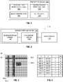
- FIG. 1 is a block diagram of a CPM support module 1000 for performing support operations, in accordance with various embodiments.
- the CPM support module 1000 may be implemented by circuitry (e.g., including electrical and/or optical components), such as a programmed computing device.
- the logic of the CPM support module 1000 may be included in a single computing device, or may be distributed across multiple computing devices that are in communication with each other as appropriate. Examples of computing devices that may, singly or in combination, implement the CPM support module 1000 are discussed herein with reference to the computing device 4000 of FIG. 7 , and examples of systems of interconnected computing devices, in which the CPM support module 1000 may be implemented across one or more of the computing devices, is discussed herein with reference to the CPM support system 5000 of FIG. 8 .
- the CPM whose operations are supported by the CPM support module 1000 may include any suitable type of CPM, such as a scanning electron microscope (SEM), a transmission electron microscope (TEM), a scanning transmission electron microscope (STEM), or an ion beam
- the CPM support module 1000 may include defective pixel identification logic 1002, charged particle detection logic 1004, defect masking logic 1006, and output logic 1008.
- the term "logic" may include an apparatus that is to perform a set of operations associated with the logic.
- any of the logic elements included in the CPM support module 1000 may be implemented by one or more computing devices programmed with instructions to cause one or more processing devices of the computing devices to perform the associated set of operations.
- a logic element may include one or more non-transitory computer-readable media having instructions thereon that, when executed by one or more processing devices of one or more computing devices, cause the one or more computing devices to perform the associated set of operations.
- module may refer to a collection of one or more logic elements that, together, perform a function associated with the module. Different ones of the logic elements in a module may take the same form or may take different forms. For example, some logic in a module may be implemented by a programmed general-purpose processing device, while other logic in a module may be implemented by an application-specific integrated circuit (ASIC). In another example, different ones of the logic elements in a module may be associated with different sets of instructions executed by one or more processing devices.
- ASIC application-specific integrated circuit
- a module may not include all of the logic elements depicted in the associated drawing; for example, a module may include a subset of the logic elements depicted in the associated drawing when that module is to perform a subset of the operations discussed herein with reference to that module.
- the CPM support module 1000 may be implemented by programmed field programmable gate arrays (FPGAs) that may be part of a charged particle camera.
- the defective pixel identification logic 1002 may be configured to identify a defective pixel region 104 of a charged particle camera 1102 (e.g., a charged particle counting camera, such as an electron counting camera).
- a "defective pixel region" of a charged particle camera 1102 may include one or more pixels that, unlike other "non-defective" pixel regions of the charged particle camera, are unable to properly detect charged particle events.
- FIG. 2 is a block diagram of a CPM system 1110 that includes a charged particle camera 1102 communicatively coupled to a data storage 1106 (e.g., multiple hard drives).
- the charged particle camera 1102 may be used as part of a CPM (e.g., the CPM 5010 discussed below with reference to FIG. 8 ) to image a specimen, and the CPM support module 1000 may generate data (to be stored in the data storage 1106) representative of charged particle events in this imaging. Data stored in the data storage 1106 may be accessible by reconstruction logic that may perform single particle analysis (SPA), tomographic reconstruction, or any other suitable reconstruction technique using the data generated by the charged particle camera 1102 to reconstruct the microscopic structure of the specimen.
- the charged particle camera 1102 may include a charged particle sensor 1104 communicatively coupled to a CPM support module 1000 (e.g., any of the CPM support modules 1000 disclosed herein).
- the charged particle sensor 1104 may take any suitable form for detecting appropriate charged particles.
- the charged particle sensor 1104 may include complementing metal oxide semiconductor (CMOS) sensor pixels for electron detection.
- CMOS complementary metal oxide semiconductor
- the defective pixel identification logic 1002 of a CPM support module 1000 may identify one or more defective pixel regions 104 of the charged particle sensor 1104 of a charged particle camera 1102, and may store the identification of the one or more defective pixel regions 104 in a memory accessible by the defective pixel identification logic 1002 (e.g., the defective pixel identification logic 1002 may store identifiers of which pixels 102 in a pixel array 100, as discussed below with reference to FIG. 3 , are defective).
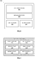
- FIG. 3 illustrates example defective pixel regions 104 of a pixel array 100 (made up of individual pixels 102) of a charged particle sensor 1104 that may be identified by the defective pixel identification logic 1002, in accordance with various embodiments.
- FIG. 3 illustrates three particular example defective pixel regions 104: a defective region 104-1 that includes a row of defective pixels 102 (also referred to as a "row defect," an example of a "line defect"), a defective pixel region 104-2 that includes a column of defective pixels 102 (also referred to as a "column defect," another example of a "line defect”), a defective region 104-3 that includes two adjacent columns of defective pixels 102 (also referred to as a "double column defect”), and a defective region 104-4 that includes a rectangular 3 ⁇ 4 array of defective pixels 102 (also referred to as an "area defect").
- a defective pixel region 104 may include a single pixel 102, and/or one or more non-rectangular areas of pixels.
- the defective pixel identification logic 1002 may store the identification of defective pixel regions 104 of a charged particle camera 1102 when the charged particle camera 1102 is manufactured or initially sold. For example, during manufacturing or test, defective pixel regions 104 of a charged particle sensor 1104 may be identified, and the defective pixel identification logic 1002 may store information regarding these defective pixel regions 104. In some embodiments, the defective pixel identification logic 1002 may "update" or otherwise store new information about defective pixel regions 104 of a charged particle camera 1102 after commencement of operation of the charged particle camera 1102.
- the defective pixel identification logic 1002 may perform periodic tests of the pixels 102 of a pixel array 100 of a charged particle sensor 1104, and when pixels 102 are newly identified (or confirmed) as defective (e.g., due to radiation damage or other deterioration), the defective pixel identification logic 1002 may update the stored list or other identification of the defective pixel regions 104 accordingly. In this manner, the defective pixel identification logic 1002 may continue to monitor the pixels 102 for defects during the lifetime of the charged particle camera 1102.
- the charged particle detection logic 1004 may be configured to generate charged particle event indicators based on charged particle events detected by the non-defective pixels 102 of the pixel array 100 of a charged particle sensor 1104.
- the charged particle detection logic 1004 may receive information about this charged particle event from the charged particle sensor 1104 (e.g., via a fiber-optic cable or other communication link), and in response, the charged particle detection logic 1004 may generate a charged particle event indicator representative of this charged particle event.
- the charged particle event indicator may identify a time and a location of the charged particle event.
- the time of a charged particle event indicator may be a frame interval N, representative of the associated charged particle event happening during the frame interval associated with the capture of the Nth frame of pixel array data; combining the frame number N with the frame rate may allow a time (e.g., in the unit of seconds) to be identified.
- the location of a charged particle event indicator may reflect the particular pixel 102 (and/or subpixels, or other locations) at which the associated charged particle event was detected.
- Charged particle event indicators generated by the charged particle detection logic 1004 may include other charged particle event information in addition to time and location, as desired.
- the defect masking logic 1006 may also be configured to generate charged particle event indicators, but these charged particle event indicators may not correspond to "detected” charged particle events detected by a charged particle camera 1102. Instead, the defect masking logic 1006 may generate "mask” (or “fake”) charged particle event indicators associated with locations within one or more of the defective pixel regions 104.
- the defect masking logic 1006 may generate the charged particle event indicators for a defective pixel 102 based on an estimate of the local charged particle radiation dose rate at the defective pixel 102, and such an estimate may rely on the "detected" charged particle events occurring at non-defective pixels 102 of a charged particle camera 1102. Thus, the defect masking logic 1006 may generate charged particle event indicators based on the charged particle events occurring at the non-defective pixels 102. In some embodiments, the defect masking logic 1006 may apply deterministic criteria to generate charged particle event indicators based on the charged particle events occurring at the non-defective pixels 102 of a charged particle camera 1102.
- the defect masking logic 1006 may generate a "mask" charged particle event indicator whose location corresponds to a defective pixel 102 when a majority of the non-defective pixels 102 closest to the defective pixel 102 detect a charged particle event (e.g., within a single frame interval or other time period).
- the deterministic criteria that may be applied by the defect masking logic 1006 may be chosen in any desired manner.
- the defect masking logic 1006 may apply probabilistic criteria to generate charged particle event indicators based on the charged particle events occurring (and not occurring) at the non-defective pixels 102 of the charged particle camera 1102. For example, the defect masking logic 1006 may generate a "mask" charged particle event indicator whose location corresponds to a defective pixel 102 with a probability that increases with the number of neighboring (e.g., one or more spatially neighboring or otherwise proximate and/or temporally neighboring or otherwise proximate) non-defective pixels 102 that detected a charged particle event (e.g., within a single frame interval or other time).
- neighboring e.g., one or more spatially neighboring or otherwise proximate and/or temporally neighboring or otherwise proximate
- a defective pixel 102 X in a "column defect" defective pixel region 104 may have "left-right" neighboring pixels 102 A and B (such that the defective pixel 102 X is between neighboring pixel 102 A and neighboring pixel 102 B), and the defect masking logic 1006 may generate a charged particle event indicator corresponding to the defective pixel 102 X in a frame interval N with probability zero when no charged particle events are detected by pixels 102 A and B in the frame interval N, with probability 0.5 when a charged particle event is detected by pixel 102 A in the frame interval N but not by the pixel 102 B (and vice versa), and with probability 1 when a charged particle event is detected by both pixels 102 A and B in the frame interval N.
- This probabilistic rule may be represented as shown in Table 1 below, wherein a "0" in the A and B columns indicates no charged particle event is detected by the associated pixel 102, and a "1" in the A and B columns indicates that a charged particle event is detected by the associated pixel 102.
- the parameter d in the embodiments disclosed herein may represent an average or expected dose rate in charged particles (e.g., electrons) per pixel per frame, and may be estimated based on past frames.
- the parameter d may be static or dynamic (e.g., may change over time as a function of imaging performance, such as a running estimate of dose rate).
- Table 2 A B P(X) 0 0 ⁇ 0 1 1 2 ⁇ + 1 2 1 ⁇ ⁇ 1 0 1 2 ⁇ + 1 2 1 ⁇ ⁇ 1 1 (1 - ⁇ )
- the parameters g A and g B in the embodiments disclosed herein may be "gain factors" that are to be applied to the neighboring pixels 102 A and 102 B. Table 3.
- the defect masking logic 1006 may generate a charged particle event indicator corresponding to defective pixels 102 X1 and X2 in a "double column defect" defective pixel region 104 (like the defective pixel region 104-3 of FIG. 3 ) when the defective pixel 102 X1 has "left-right” closest neighboring pixels 102 A and X2 (such that the defective pixel 102 X1 is between neighboring pixel 102 A and neighboring pixel 102 X2) and the defective pixel 102 X2 has "left-right” closest neighboring pixels 102 X1 and B (such that the defective pixel 102 X2 is between neighboring pixel 102 X1 and neighboring pixel 102 B), in accordance with the probabilistic rule of Table 4.
- the defect masking logic 1006 may implement any suitable deterministic criteria, probabilistic criteria, and/or combination of deterministic criteria and probabilistic criteria for generating the "mask" charged particle event indicators.
- the defect masking logic 1006 may apply a probabilistic rule for the generation of a charged particle event indicator for a defective pixel 102 in which the "influence" of charged particle events happening at non-defective pixels 102 decreases as the distance between the defective pixel 102 and the non-defective pixel 102 increases.
- the defect masking logic 1006 may similarly generate “mask” charged particle event indicators for defective pixel regions 104 in one frame interval or other time period based on "detected” charged particle events in a different frame interval or other time period (e.g., temporally "adjacent" frame intervals or other time periods).
- the defect masking logic 1006 may apply a probabilistic rule for the generation of a charged particle event indicator for a defective pixel 102 at a particular time in which the "influence" of charged particle events happening at non-defective pixels 102 at different times decreases as the temporal distance between the particular time and the different times increases.
- the defect masking logic 1006 may generate "mask" charged particle event indicators (including location and time information) for defective pixel regions 104 based on deterministic and/or probabilistic criteria relating to the location of "detected” charged particle events and/or based on deterministic and/or probabilistic criteria relating to the time of "detected” charged particle events.
- the output logic 1008 may be configured to output data representative of the charged particle event indicators generated by the charged particle detection logic 1004 (i.e., representing "detected” charged particle events) and the defect masking logic 1006 (i.e., representing "mask” charged particle events).
- FIG. 4 is a table of example charged particle event indicators (corresponding to the rows of the table) that may be output by the output logic 1008, in accordance with various embodiments.
- Each of the charged particle event indicators depicted in FIG. 4 includes location information (i.e., the x and y coordinates) and time information (i.e., a frame number).
- the charged particle event indicators provided by the output logic 1008 may also include an indicator of whether the charged particle event indicator corresponds to a "detected” charged particle event (and was therefore generated by the charged particle detection logic 1004) or to a "mask” charged particle event (was therefore generated by the defect masking logic 1006).
- the charged particle event indicators of FIG. 4 also include a "d(etected)/m(ask") indicator, with a "d” indicating that the charged particle event indicator corresponds to a "detected” charged particle event and an "m” indicating that the charged particle event indicator corresponds to a "mask” charged particle event.
- the charged particle event indicators provided by the output logic 1008 may not include an indicator of whether the charged particle event indicator corresponds to a "detected” or a "mask” charged particle event.
- the output logic 1008 may output the charged particle event indicators to reconstruction logic (e.g., via the data storage 1106) that is to use the data to perform SPA, tomographic reconstruction, or other reconstruction techniques and thereby obtain information about the specimen imaged by the charged particle camera 1102.
- Charged particle event indicators may be output by the output logic 1008 (e.g., to the data storage 1106 of the CPM system 1110 via an ethernet cable or any other suitable communication link) in any of a number of ways.
- the data output by the output logic 1008 may include a charged particle event representation data (e.g., electron event representation (EER) data).
- EER electron event representation
- the output logic 1008 may stream the charged particle event indicators as they are generated by the charged particle detection logic 1004 and the defect masking logic 1006.
- the output logic 1008 may queue or buffer the charged particle event indicators (e.g., so the defect masking logic 1006 can generate "mask” charged particle event indicators for a particular time based on "detected” charged particle events happening after that time).
- the output logic 1008 may encode the charged particle event indicators and any desired manner; for example, the output logic 1008 may output the charged particle event indicators as a stream of packets.
- the output logic 1008 may provide a first data stream that includes charged particle event indicators generated by the charged particle detection logic 1004 (i.e., associated with "detected” charged particle events) and a second, different data stream that includes charged particle event indicators generated by the defect masking logic 1006 (i.e., associated with "mask” charged particle events).
- Data representative of charged particle event indicators, output by the output logic 1008, may not include the charged particle event indicators themselves.
- the output logic 1008 may output an image or other summary of charged particle event indicators; such an image or other summary may represent a collection of charged particle event indicators (detected and/or masked), and may be collected over time such that the particular times associated with the charged particle event indicators is not represented in the image or other summary.
- the output logic 1008 may output information about the defective pixel regions 104 (e.g., to the data storage 1106 of the CPM system 1110) in addition to the charged particle event indicators.
- the output logic 1008 may include identification information about the defective pixel regions 104 (e.g., the locations of defective pixel regions 104 as identified by the defective pixel identification logic 1002) in headers of data streams that include charged particle event indicators.
- the output logic 1008 may provide a first data stream that includes charged particle event indicators and a second, different data stream that includes information about the defective pixel regions 104.
- the defective pixel identification logic 1002 and/or the output logic 1008 may include identification information about the defective pixel regions 104 as separate files that can be stored alongside the charged particle event indicators (e.g., in the data storage 1106) or may be otherwise accessed.
- Such files be provided in any suitable format, such as Extensible Markup Language (XML), JavaScript Object Notation (JSON), or Comma-Separated Value (CSV).
- XML Extensible Markup Language
- JSON JavaScript Object Notation
- CSV Comma-Separated Value
- FIG. 5 is a flow diagram of a method 2000 of performing CPM support operations, in accordance with various embodiments.
- the operations of the method 2000 may be illustrated with reference to particular embodiments disclosed herein (e.g., the CPM support modules 1000 discussed herein with reference to FIG. 1 , the GUI 3000 discussed herein with reference to FIG. 6 , the computing devices 4000 discussed herein with reference to FIG. 7 , and/or the CPM support system 5000 discussed herein with reference to FIG. 8 ), the method 2000 may be used in any suitable setting to perform any suitable CPM support operations. Operations are illustrated once each and in a particular order in FIG. 5 , but the operations may be reordered and/or repeated as desired and appropriate (e.g., different operations performed may be performed in parallel, as suitable).
- a defective pixel region of a charged particle camera may be identified, wherein the charged particle camera cannot detect charged particle events in the defective pixel region.
- the defective pixel identification logic 1002 of a CPM support module 1000 may perform the operations of 2002 in accordance with any of the embodiments disclosed herein.
- a first charged particle event indicator that identifies a first time and a first location of a first charged particle event outside the defective pixel region may be generated, wherein the first charged particle event is detected by the charged particle camera.
- the charged particle detection logic 1004 of a CPM support module 1000 may perform the operations of 2004 in accordance with any of the embodiments disclosed herein.
- a second charged particle event indicator that identifies a second time and a second location in the defective pixel region may be generated.
- the defect masking logic 1006 of a CPM support module 1000 may perform the operations of 2006 in accordance with any of the embodiments disclosed herein.
- data representative of the charged particle event indicators may be output.
- the output logic 1008 of a CMP support module 1000 may perform the operations of 2008 in accordance with any of the embodiments disclosed herein.
- the CPM support methods disclosed herein may include interactions with a human user (e.g., via the user local computing device 5020 discussed herein with reference to FIG. 8 ). These interactions may include providing information to the user (e.g., information regarding the operation of a CPM such as the CPM 5010 of FIG. 8 , information regarding a sample being analyzed or other test or measurement performed by a CPM, information retrieved from a local or remote database, or other information) or providing an option for a user to input commands (e.g., to control the operation of a CPM such as the CPM 5010 of FIG. 8 , or to control the analysis of data generated by a CPM), queries (e.g., to a local or remote database), or other information.
- information to the user e.g., information regarding the operation of a CPM such as the CPM 5010 of FIG. 8 , information regarding a sample being analyzed or other test or measurement performed by a CPM, information retrieved from a local or remote database, or other information
- these interactions may be performed through a graphical user interface (GUI) that includes a visual display on a display device (e.g., the display device 4010 discussed herein with reference to FIG. 7 ) that provides outputs to the user and/or prompts the user to provide inputs (e.g., via one or more input devices, such as a keyboard, mouse, trackpad, or touchscreen, included in the other I/O devices 4012 discussed herein with reference to FIG. 7 ).
- GUI graphical user interface
- the CPM support systems disclosed herein may include any suitable GUIs for interaction with a user.
- FIG. 6 depicts an example GUI 3000 that may be used in the performance of some or all of the support methods disclosed herein, in accordance with various embodiments.
- the GUI 3000 may be provided on a display device (e.g., the display device 4010 discussed herein with reference to FIG. 7 ) of a computing device (e.g., the computing device 4000 discussed herein with reference to FIG. 7 ) of a CPM support system (e.g., the CPM support system 5000 discussed herein with reference to FIG. 8 ), and a user may interact with the GUI 3000 using any suitable input device (e.g., any of the input devices included in the other I/O devices 4012 discussed herein with reference to FIG. 7 ) and input technique (e.g., movement of a cursor, motion capture, facial recognition, gesture detection, voice recognition, actuation of buttons, etc.).
- input technique e.g., movement of a cursor, motion capture, facial recognition, gesture detection, voice recognition, actuation of buttons, etc.
- the GUI 3000 may include a data display region 3002, a data analysis region 3004, a CPM control region 3006, and a settings region 3008.
- the particular number and arrangement of regions depicted in FIG. 6 is simply illustrative, and any number and arrangement of regions, including any desired features, may be included in a GUI 3000.
- the data display region 3002 may display data generated by a CPM (e.g., the CPM 5010 discussed herein with reference to FIG. 8 ).
- the data display region 3002 may display charged particle event indicators output by the output logic 1008 of a CPM support module 1000.
- the data analysis region 3004 may display the results of data analysis (e.g., the results of analyzing the data illustrated in the data display region 3002 and/or other data).
- the data analysis region 3004 may display a reconstruction or other representation of a specimen imaged in accordance with any of the techniques disclosed herein.
- the data display region 3002 and the data analysis region 3004 may be combined in the GUI 3000 (e.g., to include data output from a CPM, and some analysis of the data, in a common graph or region).
- the CPM control region 3006 may include options that allow the user to control a CPM (e.g., the CPM 5010 discussed herein with reference to FIG. 8 ).
- the CPM control region 3006 may include control options to program, start, or stop imaging operations.
- the settings region 3008 may include options that allow the user to control the features and functions of the GUI 3000 (and/or other GUIs) and/or perform common computing operations with respect to the data display region 3002 and data analysis region 3004 (e.g., saving data on a storage device, such as the storage device 4004 discussed herein with reference to FIG. 7 , sending data to another user, labeling data, etc.).
- the settings region 3008 may include information about defective pixel regions 104 of the charged particle camera 1102 (e.g., as identified by the defective pixel identification logic 1002) or controls to allow a user to view and/or change the criteria used by the defect masking logic 1006 when generating "mask" charged particle event indicators).
- the CPM support module 1000 may be implemented by one or more computing devices.
- FIG. 7 is a block diagram of a computing device 4000 that may perform some or all of the CPM support methods disclosed herein, in accordance with various embodiments.
- the CPM support module 1000 may be implemented by a single computing device 4000 or by multiple computing devices 4000.
- a computing device 4000 (or multiple computing devices 4000) that implements the CPM support module 1000 may be part of one or more of the CPM 5010, the user local computing device 5020, the service local computing device 5030, or the remote computing device 5040 of FIG. 8 .
- the computing device 4000 of FIG. 7 is illustrated as having a number of components, but any one or more of these components may be omitted or duplicated, as suitable for the application and setting.
- some or all of the components included in the computing device 4000 may be attached to one or more motherboards and enclosed in a housing (e.g., including plastic, metal, and/or other materials).
- some these components may be fabricated onto a single system-on-a-chip (SoC) (e.g., an SoC may include one or more processing devices 4002 and one or more storage devices 4004).
- SoC system-on-a-chip
- the computing device 4000 may not include one or more of the components illustrated in FIG.
- the computing device 4000 may not include a display device 4010, but may include display device interface circuitry (e.g., a connector and driver circuitry) to which a display device 4010 may be coupled.
- a display device 4010 may include display device interface circuitry (e.g., a connector and driver circuitry) to which a display device 4010 may be coupled.
- the computing device 4000 may include a processing device 4002 (e.g., one or more processing devices).
- processing device may refer to any device or portion of a device that processes electronic data from registers and/or memory to transform that electronic data into other electronic data that may be stored in registers and/or memory.
- the processing device 4002 may include one or more digital signal processors (DSPs), application-specific integrated circuits (ASICs), central processing units (CPUs), graphics processing units (GPUs), cryptoprocessors (specialized processors that execute cryptographic algorithms within hardware), server processors, or any other suitable processing devices.
- DSPs digital signal processors
- ASICs application-specific integrated circuits
- CPUs central processing units
- GPUs graphics processing units
- cryptoprocessors specialized processors that execute cryptographic algorithms within hardware
- server processors or any other suitable processing devices.
- the computing device 4000 may include a storage device 4004 (e.g., one or more storage devices).
- the storage device 4004 may include one or more memory devices such as random access memory (RAM) (e.g., static RAM (SRAM) devices, magnetic RAM (MRAM) devices, dynamic RAM (DRAM) devices, resistive RAM (RRAM) devices, or conductive-bridging RAM (CBRAM) devices), hard drive-based memory devices, solid-state memory devices, networked drives, cloud drives, or any combination of memory devices.
- RAM random access memory
- SRAM static RAM
- MRAM magnetic RAM
- DRAM dynamic RAM
- RRAM resistive RAM
- CBRAM conductive-bridging RAM
- the storage device 4004 may include memory that shares a die with a processing device 4002.
- the memory may be used as cache memory and may include embedded dynamic random-access memory (eDRAM) or spin transfer torque magnetic random-access memory (STT-MRAM), for example.
- the storage device 4004 may include non-transitory computer readable media having instructions thereon that, when executed by one or more processing devices (e.g., the processing device 4002), cause the computing device 4000 to perform any appropriate ones of or portions of the methods disclosed herein.
- the computing device 4000 may include an interface device 4006 (e.g., one or more interface devices 4006).
- the interface device 4006 may include one or more communication chips, connectors, and/or other hardware and software to govern communications between the computing device 4000 and other computing devices.
- the interface device 4006 may include circuitry for managing wireless communications for the transfer of data to and from the computing device 4000.
- wireless and its derivatives may be used to describe circuits, devices, systems, methods, techniques, communications channels, etc., that may communicate data through the use of modulated electromagnetic radiation through a nonsolid medium. The term does not imply that the associated devices do not contain any wires, although in some embodiments they might not.
- Circuitry included in the interface device 4006 for managing wireless communications may implement any of a number of wireless standards or protocols, including but not limited to Institute for Electrical and Electronic Engineers (IEEE) standards including Wi-Fi (IEEE 802.11 family), IEEE 802.16 standards (e.g., IEEE 802.16-2005 Amendment), Long-Term Evolution (LTE) project along with any amendments, updates, and/or revisions (e.g., advanced LTE project, ultra-mobile broadband (UMB) project (also referred to as "3GPP2”), etc.).
- IEEE Institute for Electrical and Electronic Engineers
- Wi-Fi IEEE 802.11 family
- IEEE 802.16 standards e.g., IEEE 802.16-2005 Amendment
- LTE Long-Term Evolution
- LTE Long-Term Evolution
- UMB ultra-mobile broadband
- circuitry included in the interface device 4006 for managing wireless communications may operate in accordance with a Global System for Mobile Communication (GSM), General Packet Radio Service (GPRS), Universal Mobile Telecommunications System (UMTS), High Speed Packet Access (HSPA), Evolved HSPA (E-HSPA), or LTE network.
- GSM Global System for Mobile Communication
- GPRS General Packet Radio Service
- UMTS Universal Mobile Telecommunications System
- E-HSPA Evolved HSPA
- LTE LTE network.
- circuitry included in the interface device 4006 for managing wireless communications may operate in accordance with Enhanced Data for GSM Evolution (EDGE), GSM EDGE Radio Access Network (GERAN), Universal Terrestrial Radio Access Network (UTRAN), or Evolved UTRAN (E-UTRAN).
- EDGE Enhanced Data for GSM Evolution
- GERAN GSM EDGE Radio Access Network
- UTRAN Universal Terrestrial Radio Access Network
- E-UTRAN Evolved UTRAN
- circuitry included in the interface device 4006 for managing wireless communications may operate in accordance with Code Division Multiple Access (CDMA), Time Division Multiple Access (TDMA), Digital Enhanced Cordless Telecommunications (DECT), Evolution-Data Optimized (EV-DO), and derivatives thereof, as well as any other wireless protocols that are designated as 3G, 4G, 5G, and beyond.
- the interface device 4006 may include one or more antennas (e.g., one or more antenna arrays) to receipt and/or transmission of wireless communications.
- the interface device 4006 may include circuitry for managing wired communications, such as electrical, optical, or any other suitable communication protocols.
- the interface device 4006 may include circuitry to support communications in accordance with Ethernet technologies.
- the interface device 4006 may support both wireless and wired communication, and/or may support multiple wired communication protocols and/or multiple wireless communication protocols.
- a first set of circuitry of the interface device 4006 may be dedicated to shorter-range wireless communications such as Wi-Fi or Bluetooth
- a second set of circuitry of the interface device 4006 may be dedicated to longer-range wireless communications such as global positioning system (GPS), EDGE, GPRS, CDMA, WiMAX, LTE, EV-DO, or others.
- GPS global positioning system
- EDGE EDGE
- GPRS CDMA
- WiMAX Long Term Evolution
- LTE Long Term Evolution
- EV-DO or others.
- a first set of circuitry of the interface device 4006 may be dedicated to wireless communications
- the computing device 4000 may include battery/power circuitry 4008.
- the battery/power circuitry 4008 may include one or more energy storage devices (e.g., batteries or capacitors) and/or circuitry for coupling components of the computing device 4000 to an energy source separate from the computing device 4000 (e.g., AC line power).
- the computing device 4000 may include a display device 4010 (e.g., multiple display devices).
- the display device 4010 may include any visual indicators, such as a heads-up display, a computer monitor, a projector, a touchscreen display, a liquid crystal display (LCD), a light-emitting diode display, or a flat panel display.
- a display device 4010 may include any visual indicators, such as a heads-up display, a computer monitor, a projector, a touchscreen display, a liquid crystal display (LCD), a light-emitting diode display, or a flat panel display.
- the computing device 4000 may include other input/output (I/O) devices 4012.
- the other I/O devices 4012 may include one or more audio output devices (e.g., speakers, headsets, earbuds, alarms, etc.), one or more audio input devices (e.g., microphones or microphone arrays), location devices (e.g., GPS devices in communication with a satellite-based system to receive a location of the computing device 4000, as known in the art), audio codecs, video codecs, printers, sensors (e.g., thermocouples or other temperature sensors, humidity sensors, pressure sensors, vibration sensors, accelerometers, gyroscopes, etc.), image capture devices such as cameras, keyboards, cursor control devices such as a mouse, a stylus, a trackball, or a touchpad, bar code readers, Quick Response (QR) code readers, or radio frequency identification (RFID) readers, for example.
- audio output devices e.g., speakers, headsets, earbuds, alarms,
- the computing device 4000 may have any suitable form factor for its application and setting, such as a handheld or mobile computing device (e.g., a cell phone, a smart phone, a mobile internet device, a tablet computer, a laptop computer, a netbook computer, an ultrabook computer, a personal digital assistant (PDA), an ultra-mobile personal computer, etc.), a desktop computing device, or a server computing device or other networked computing component.
- a handheld or mobile computing device e.g., a cell phone, a smart phone, a mobile internet device, a tablet computer, a laptop computer, a netbook computer, an ultrabook computer, a personal digital assistant (PDA), an ultra-mobile personal computer, etc.
- PDA personal digital assistant
- FIG. 8 is a block diagram of an example CPM support system 5000 in which some or all of the CPM support methods disclosed herein may be performed, in accordance with various embodiments.
- the CPM support modules and methods disclosed herein e.g., the CPM support module 1000 of FIG. 1 and the method 2000 of FIG. 5
- any of the CPM 5010, the user local computing device 5020, the service local computing device 5030, or the remote computing device 5040 may include any of the embodiments of the computing device 4000 discussed herein with reference to FIG. 7 , and any of the CPM 5010, the user local computing device 5020, the service local computing device 5030, or the remote computing device 5040 may take the form of any appropriate ones of the embodiments of the computing device 4000 discussed herein with reference to FIG. 7 .
- the CPM 5010, the user local computing device 5020, the service local computing device 5030, or the remote computing device 5040 may each include a processing device 5002, a storage device 5004, and an interface device 5006.
- the processing device 5002 may take any suitable form, including the form of any of the processing devices 4002 discussed herein with reference to FIG. 4 , and the processing devices 5002 included in different ones of the CPM 5010, the user local computing device 5020, the service local computing device 5030, or the remote computing device 5040 may take the same form or different forms.
- the storage device 5004 may take any suitable form, including the form of any of the storage devices 5004 discussed herein with reference to FIG.
- the interface device 5006 may take any suitable form, including the form of any of the interface devices 4006 discussed herein with reference to FIG. 4 , and the interface devices 5006 included in different ones of the CPM 5010, the user local computing device 5020, the service local computing device 5030, or the remote computing device 5040 may take the same form or different forms.
- the CPM 5010, the user local computing device 5020, the service local computing device 5030, and the remote computing device 5040 may be in communication with other elements of the CPM support system 5000 via communication pathways 5008.
- the communication pathways 5008 may communicatively couple the interface devices 5006 of different ones of the elements of the CPM support system 5000, as shown, and may be wired or wireless communication pathways (e.g., in accordance with any of the communication techniques discussed herein with reference to the interface devices 4006 of the computing device 4000 of FIG. 7 ).
- a service local computing device 5030 may not have a direct communication pathway 5008 between its interface device 5006 and the interface device 5006 of the CPM 5010, but may instead communicate with the CPM 5010 via the communication pathway 5008 between the service local computing device 5030 and the user local computing device 5020 and the communication pathway 5008 between the user local computing device 5020 and the CPM 5010.
- the user local computing device 5020 may be a computing device (e.g., in accordance with any of the embodiments of the computing device 4000 discussed herein) that is local to a user of the CPM 5010. In some embodiments, the user local computing device 5020 may also be local to the CPM 5010, but this need not be the case; for example, a user local computing device 5020 that is in a user's home or office may be remote from, but in communication with, the CPM 5010 so that the user may use the user local computing device 5020 to control and/or access data from the CPM 5010. In some embodiments, the user local computing device 5020 may be a laptop, smartphone, or tablet device. In some embodiments the user local computing device 5020 may be a portable computing device.
- the service local computing device 5030 may be a computing device (e.g., in accordance with any of the embodiments of the computing device 4000 discussed herein) that is local to an entity that services the CPM 5010.
- the service local computing device 5030 may be local to a manufacturer of the CPM 5010 or to a third-party service company.
- the service local computing device 5030 may communicate with the CPM 5010, the user local computing device 5020, and/or the remote computing device 5040 (e.g., via a direct communication pathway 5008 or via multiple "indirect” communication pathways 5008, as discussed above) to receive data regarding the operation of the CPM 5010, the user local computing device 5020, and/or the remote computing device 5040 (e.g., the results of self-tests of the CPM 5010, calibration coefficients used by the CPM 5010, the measurements of sensors associated with the CPM 5010, etc.).
- the service local computing device 5030 may communicate with the CPM 5010, the user local computing device 5020, and/or the remote computing device 5040 (e.g., via a direct communication pathway 5008 or via multiple "indirect” communication pathways 5008, as discussed above) to transmit data to the CPM 5010, the user local computing device 5020, and/or the remote computing device 5040 (e.g., to update programmed instructions, such as firmware, in the CPM 5010, to initiate the performance of test or calibration sequences in the CPM 5010, to update programmed instructions, such as software, in the user local computing device 5020 or the remote computing device 5040, etc.).
- programmed instructions such as firmware, in the CPM 5010
- the remote computing device 5040 e.g., to update programmed instructions, such as software, in the user local computing device 5020 or the remote computing device 5040, etc.
- a user of the CPM 5010 may utilize the CPM 5010 or the user local computing device 5020 to communicate with the service local computing device 5030 to report a problem with the CPM 5010 or the user local computing device 5020, to request a visit from a technician to improve the operation of the CPM 5010, to order consumables or replacement parts associated with the CPM 5010, or for other purposes.
- the remote computing device 5040 may be a computing device (e.g., in accordance with any of the embodiments of the computing device 4000 discussed herein) that is remote from the CPM 5010 and/or from the user local computing device 5020.
- the remote computing device 5040 may be included in a datacenter or other large-scale server environment.
- the remote computing device 5040 may include network-attached storage (e.g., as part of the storage device 5004).
- the remote computing device 5040 may store data generated by the CPM 5010, perform analyses of the data generated by the CPM 5010 (e.g., in accordance with programmed instructions), facilitate communication between the user local computing device 5020 and the CPM 5010, and/or facilitate communication between the service local computing device 5030 and the CPM 5010.
- a CPM support system 5000 may include multiple user local computing devices 5020 (e.g., different user local computing devices 5020 associated with different users or in different locations).
- a CPM support system 5000 may include multiple CPMs 5010, all in communication with service local computing device 5030 and/or a remote computing device 5040; in such an embodiment, the service local computing device 5030 may monitor these multiple CPMs 5010, and the service local computing device 5030 may cause updates or other information may be "broadcast" to multiple CPMs 5010 at the same time.
- Different ones of the CPMs 5010 in a CPM support system 5000 may be located close to one another (e.g., in the same room) or farther from one another (e.g., on different floors of a building, in different buildings, in different cities, etc.).
- a CPM 5010 may be connected to an Internet-of-Things (loT) stack that allows for command and control of the CPM 5010 through a web-based application, a virtual or augmented reality application, a mobile application, and/or a desktop application. Any of these applications may be accessed by a user operating the user local computing device 5020 in communication with the CPM 5010 by the intervening remote computing device 5040.
- a CPM 5010 may be sold by the manufacturer along with one or more associated user local computing devices 5020 as part of a local CPM computing unit 5012.
- Example 1 is a charged particle microscope support apparatus, including: first logic to identify a defective pixel region of a charged particle camera, wherein the charged particle camera cannot detect charged particle events in the defective pixel region; second logic to generate a first charged particle event indicator that identifies a first time and a first location of a first charged particle event outside the defective pixel region, wherein the first charged particle event is detected by the charged particle camera; third logic to generate a second charged particle event indicator that identifies a second time and a second location in the defective pixel region; and fourth logic to output data representative of the charged particle event indicators.
- Example 2 includes the subject matter of Example 1, and further specifies that the second charged particle event indicator is not representative of a charged particle event detected by the charged particle camera.
- Example 3 includes the subject matter of any of Examples 1-2, and further specifies that the third logic is to generate the second charged particle event indicator based at least in part on the first charged particle event.
- Example 4 includes the subject matter of any of Examples 1-3, and further specifies that the third logic is to generate the second charged particle event indicator based at least in part on the first time.
- Example 5 includes the subject matter of any of Examples 1-4, and further specifies that the third logic is to generate the second charged particle event indicator based at least in part on the first location.
- Example 6 includes the subject matter of any of Examples 1-5, and further specifies that the third logic is to generate the second charged particle event indicator probabilistically based at least in part on the first charged particle event.
- Example 7 includes the subject matter of any of Examples 1-6, and further specifies that the first location is adjacent to the second location.
- Example 8 includes the subject matter of any of Examples 1-7, and further specifies that the first time is equal to the second time.
- Example 9 includes the subject matter of any of Examples 1-8, and further specifies that the first time is associated with a same frame as the second time.
- Example 10 includes the subject matter of any of Examples 1-9, and further specifies that the data output by the fourth logic is representative of a charged particle event not occurring at a third time and third location, and the third logic is to generate the second charged particle event indicator probabilistically based at least in part on the charged particle event not occurring at the third time and third location.
- Example 11 includes the subject matter of Example 10, and further specifies that the second location is adjacent to the third location.
- Example 12 includes the subject matter of any of Examples 10-11, and further specifies that the second time is equal to the third time.
- Example 13 includes the subject matter of any of Examples 1-12, and further specifies that the second time is associated with a same frame as the third time.
- Example 14 includes the subject matter of any of Examples 1-13, and further specifies that the third logic is to generate the second charged particle event indicator probabilistically based at least in part on a distance between the first location and the second location.
- Example 15 includes the subject matter of Example 14, and further specifies that the data output by the fourth logic is representative of a charged particle event not occurring at a third time and third location, and the third logic is to generate the second charged particle event indicator probabilistically based at least in part on a distance between the second location and the third location.
- Example 16 includes the subject matter of any of Examples 1-15, and further specifies that the third logic is to generate the second charged particle event indicator probabilistically based at least in part on a difference between the first time and the second time.
- Example 17 includes the subject matter of any of Examples 1-16, and further specifies that the data output by the fourth logic is representative of a charged particle event not occurring at a third time and third location, and the third logic is to generate the second charged particle event indicator probabilistically based at least in part on a difference between the second time and the third time.
- Example 18 includes the subject matter of any of Examples 1-17, and further specifies that the third logic is to generate the second charged particle event indicator based on one or more charged particle events occurring at one or more locations proximate to the second location.
- Example 19 includes the subject matter of Example 18, and further specifies that the one or more locations proximate to the second location are one or more locations neighboring the second location.
- Example 20 includes the subject matter of Example 19, and further specifies that the second location includes a pixel, and the one or more locations neighboring the second location are one or more pixels neighboring the pixel.
- Example 21 includes the subject matter of any of Examples 18-19, and further specifies that the one or more locations proximate to the second location includes a first proximate location and a second proximate location, and the third logic is to generate the second charged particle event indicator probabilistically with greater probability based on a charged particle event at the first proximate location than a charged particle event at the second proximate location.
- Example 22 includes the subject matter of any of Examples 18-21, and further specifies that the third logic is to generate the second charged particle event indicator probabilistically with unequal probabilities of generating the second charged particle event indicator and not generating the second charged particle event indicator.
- Example 23 includes the subject matter of any of Examples 1-22, and further specifies that the defective pixel region includes a line of pixels.
- Example 24 includes the subject matter of any of Examples 1-22, and further specifies that the defective pixel region includes a single pixel.
- Example 25 includes the subject matter of any of Examples 1-22, and further specifies that the defective pixel region includes multiple adjacent lines of pixels.
- Example 26 includes the subject matter of any of Examples 1-22, and further specifies that the defective pixel region includes a rectangular area of pixels.
- Example 27 includes the subject matter of any of Examples 1-22, and further specifies that the defective pixel region includes a non-rectangular area of pixels.
- Example 28 includes the subject matter of any of Examples 1-27, and further specifies that the data output by the fourth logic includes electron event representation (EER) data.
- EER electron event representation
- Example 29 includes the subject matter of any of Examples 1-28, and further specifies that the second charged particle event indicator identifies that the second charged particle event indicator is not representative of a detected charged particle event.
- Example 30 includes the subject matter of any of Examples 1-28, and further specifies that the second charged particle event indicator does not identify that the second charged particle event indicator is not representative of a detected charged particle event.
- Example 31 includes the subject matter of any of Examples 1-30, and further specifies that the first logic is to provide data representative of the defective pixel region in an Extensible Markup Language (XML) file, a JavaScript Object Notation (JSON) file, or a Comma-Separated Value (CSV) file.
- XML Extensible Markup Language
- JSON JavaScript Object Notation
- CSV Comma-Separated Value
- Example 32 includes the subject matter of any of Examples 1-31, and further specifies that the fourth logic is to output data representative of the defective pixel region along with the data representative of the charged particle event indicators.
- Example 33 includes the subject matter of any of Examples 1-32, and further specifies that the fourth logic is to output the data to reconstruction logic.
- Example 34 includes the subject matter of Example 33, and further specifies that the reconstruction logic is to perform single particle analysis or tomographic reconstruction.
- Example 35 includes the subject matter of any of Examples 1-34, and further specifies that the first logic, second logic, third logic, and fourth logic are included in the charged particle camera.
- Example 36 includes the subject matter of any of Examples 1-35, and further specifies that the first logic is to identify a defective pixel region by generating a list of defective pixels.
- Example 37 includes the subject matter of any of Examples 1-36, and further specifies that the first logic is to store an initial identification of the defective pixel region and to update its identification of the defective pixel region after commencement of operation of the charged particle camera.
- Example 38 includes the subject matter of any of Examples 1-37, and further specifies that the fourth logic is to output the data representative of the charged particle event indicators by streaming the data representative of the charged particle event indicators.
- Example 39 includes the subject matter of any of Examples 1-38, and further specifies that the charged particle camera is included in a charged particle microscope.
- Example 40 includes the subject matter of Example 39, and further includes: a charged particle sensor, of the charged particle camera, to detect charged particle events.
- Example 41 includes the subject matter of any of Examples 1-40, and further specifies that the second charged particle event indicator is one of a plurality of charged particle event indicators, and the third logic is to generate the plurality of charged particle event indicators that individually identify an associated time and an associated location in the defective pixel region.
- Example 42 includes the subject matter of Example 41, and further specifies that the plurality of charged particle event indicators are not representative of charged particle events detected by the charged particle camera.
- Example 43 includes the subject matter of any of Examples 41-42, and further specifies that the third logic is to generate the plurality of charged particle event indicators based at least in part on the first charged particle event.
- Example 44 includes the subject matter of any of Examples 41-43, and further specifies that the third logic is to generate the plurality of charged particle event indicators based at least in part on the first time.
- Example 45 includes the subject matter of any of Examples 41-44, and further specifies that the third logic is to generate the plurality of charged particle event indicators based at least in part on the first location.
- Example 46 includes the subject matter of any of Examples 41-45, and further specifies that the third logic is to generate the plurality of charged particle event indicators probabilistically based at least in part on the first charged particle event.
- Example 47 includes the subject matter of any of Examples 41-46, and further specifies that the associated locations are adjacent to the second location.
- Example 48 includes the subject matter of any of Examples 41-47, and further specifies that the first time is equal to the associated times.
- Example 49 includes the subject matter of any of Examples 41-48, and further specifies that the first time is associated with a same frame as the associated times.
- Example 50 is a charged particle microscope support apparatus, including: first logic to identify a defective pixel region of a charged particle camera, wherein the charged particle camera cannot detect charged particle events in the defective pixel region; second logic to generate a charged particle event indicator for a location in the defective pixel region based at least in part on one or more charged particle events detected outside the defective pixel region; and third logic to output data representative of the charged particle event indicator.
- Example 51 includes the subject matter of Example 50, and further specifies that the charged particle event indicator is not representative of a charged particle event detected by the charged particle camera.
- Example 52 includes the subject matter of any of Examples 50-51, and further specifies that the second logic is to generate the charged particle event indicator probabilistically based at least in part on one or more charged particle events detected outside the defective pixel region.
- Example 53 includes the subject matter of any of Examples 50-52, and further specifies that the location is a first location, and the one or more charged particle events detected outside the defective pixel region includes a charged particle event at least one location adjacent to the first location.
- Example 54 includes the subject matter of any of Examples 50-53, and further specifies that the second logic is to generate the charged particle event indicator probabilistically based at least in part on one or more charged particle events detected outside the defective pixel region by generating the charged particle event with a first probability when a charged particle event occurs at a location outside the defective pixel region and by generating the charged particle event with a second probability when no charged particle event occurs at the location outside the defective pixel region.
- Example 55 includes the subject matter of Example 54, and further specifies that the location outside the defective pixel region is a location adjacent to the defective pixel region.
- Example 56 includes the subject matter of any of Examples 50-55, and further specifies that the second logic is to generate the charged particle event indicator for the location in the defective pixel region in a frame capture time interval based at least in part on one or more charged particle events detected outside the defective pixel region in the frame capture time interval.
- Example 57 includes the subject matter of any of Examples 50-56, and further specifies that the second logic is to generate the charged particle event indicator for the location in the defective pixel region in a frame capture time interval based at least in part on one or more charged particle events detected outside the defective pixel region outside the frame capture time interval.
- Example 58 includes the subject matter of any of Examples 50-57, and further specifies that the second logic is to generate the charged particle event indicator probabilistically based at least in part on one or more charged particle events detected outside the defective pixel region by generating the charged particle event with a first probability when a charged particle event occurs at a first location outside the defective pixel region and by generating the charged particle event with a second probability, different from the first probability, when a charged particle event occurs at a second location, different from the first location, outside the defective pixel region.
- Example 59 includes the subject matter of any of Examples 50-58, and further specifies that the defective pixel region includes a line of pixels.
- Example 60 includes the subject matter of any of Examples 50-58, and further specifies that the defective pixel region includes a single pixel.
- Example 61 includes the subject matter of any of Examples 50-58, and further specifies that the defective pixel region includes multiple adjacent lines of pixels.
- Example 62 includes the subject matter of any of Examples 50-58, and further specifies that the defective pixel region includes a rectangular area of pixels.
- Example 63 includes the subject matter of any of Examples 50-58, and further specifies that the defective pixel region includes a non-rectangular area of pixels.
- Example 64 includes the subject matter of any of Examples 50-63, and further specifies that the data output by the third logic includes electron event representation (EER) data.
- EER electron event representation
- Example 65 includes the subject matter of any of Examples 50-64, and further specifies that the charged particle event indicator identifies that the charged particle event indicator is not representative of a detected charged particle event.
- Example 66 includes the subject matter of any of Examples 50-64, and further specifies that the charged particle event indicator does not identify that the charged particle event indicator is not representative of a detected charged particle event.
- Example 67 includes the subject matter of any of Examples 50-66, and further specifies that the first logic is to provide data representative of the defective pixel region in an Extensible Markup Language (XML) file, a JavaScript Object Notation (JSON) file, or a Comma-Separated Value (CSV) file.
- XML Extensible Markup Language
- JSON JavaScript Object Notation
- CSV Comma-Separated Value
- Example 68 includes the subject matter of any of Examples 50-67, and further specifies that the third logic is to output data representative of the defective pixel region along with the data representative of the charged particle event indicator.
- Example 69 includes the subject matter of any of Examples 50-68, and further specifies that the third logic is to output the data to reconstruction logic.
- Example 70 includes the subject matter of Example 69, and further specifies that the reconstruction logic is to perform single particle analysis or tomographic reconstruction.
- Example 71 includes the subject matter of any of Examples 50-70, and further specifies that the first logic, second logic, and third logic are included in the charged particle camera.
- Example 72 includes the subject matter of any of Examples 50-71, and further specifies that the first logic is to identify a defective pixel region by generating a list of defective pixels.
- Example 73 includes the subject matter of any of Examples 50-72, and further specifies that the first logic is to store an initial identification of the defective pixel region and to update its identification of the defective pixel region after commencement of operation of the charged particle camera.
- Example 74 includes the subject matter of any of Examples 50-73, and further specifies that the third logic is to output data representative of a plurality of charged particle event indicators by streaming the data representative of the plurality of charged particle event indicators.
- Example 75 includes the subject matter of any of Examples 50-74, and further specifies that the charged particle camera is included in a charged particle microscope.
- Example 76 includes the subject matter of Example 75, and further includes: a charged particle sensor, of the charged particle camera, to detect charged particle events.
- Example 77 is a charged particle microscope support apparatus, including: first logic to generate a first charged particle event indicator that identifies a first time and a first location of a first charged particle event outside a defective pixel region of a charged particle camera, wherein the first charged particle event is detected by the charged particle camera; second logic to generate a second charged particle event indicator that identifies a second time and a second location in the defective pixel region; and third logic to output data representative of the charged particle event indicators.
- Example 78 includes the subject matter of Example 77, and further specifies that the second charged particle event indicator is not representative of a charged particle event detected by the charged particle camera.
- Example 79 includes the subject matter of any of Examples 77-78, and further specifies that the second logic is to generate the second charged particle event indicator based at least in part on the first charged particle event.
- Example 80 includes the subject matter of any of Examples 77-79, and further specifies that the second logic is to generate the second charged particle event indicator based at least in part on the first time.
- Example 81 includes the subject matter of any of Examples 77-80, and further specifies that the second logic is to generate the second charged particle event indicator based at least in part on the first location.
- Example 82 includes the subject matter of any of Examples 77-81, and further specifies that the second logic is to generate the second charged particle event indicator probabilistically based at least in part on the first charged particle event.
- Example 83 includes the subject matter of any of Examples 77-82, and further specifies that the first location is adjacent to the second location.
- Example 84 includes the subject matter of any of Examples 77-83, and further specifies that the first time is equal to the second time.
- Example 85 includes the subject matter of any of Examples 77-84, and further specifies that the first time is associated with a same frame as the second time.
- Example 86 includes the subject matter of any of Examples 77-85, and further specifies that the data output by the third logic is representative of a charged particle event not occurring at a third time and third location, and the second logic is to generate the second charged particle event indicator probabilistically based at least in part on the charged particle event not occurring at the third time and third location.
- Example 87 includes the subject matter of Example 86, and further specifies that the second location is adjacent to the third location.
- Example 88 includes the subject matter of any of Examples 86-87, and further specifies that the second time is equal to the third time.
- Example 89 includes the subject matter of any of Examples 77-88, and further specifies that the second time is associated with a same frame as the third time.
- Example 90 includes the subject matter of any of Examples 77-89, and further specifies that the second logic is to generate the second charged particle event indicator probabilistically based at least in part on a distance between the first location and the second location.
- Example 91 includes the subject matter of Example 90, and further specifies that the data output by the third logic is representative of a charged particle event not occurring at a third time and third location, and the second logic is to generate the second charged particle event indicator probabilistically based at least in part on a distance between the second location and the third location.
- Example 92 includes the subject matter of any of Examples 77-91, and further specifies that the second logic is to generate the second charged particle event indicator probabilistically based at least in part on a difference between the first time and the second time.
- Example 93 includes the subject matter of any of Examples 77-92, and further specifies that the data output by the third logic is representative of a charged particle event not occurring at a third time and third location, and the second logic is to generate the second charged particle event indicator probabilistically based at least in part on a difference between the second time and the third time.
- Example 94 includes the subject matter of any of Examples 77-93, and further specifies that the second logic is to generate the second charged particle event indicator based on one or more charged particle events occurring at one or more locations proximate to the second location.
- Example 95 includes the subject matter of Example 94, and further specifies that the one or more locations proximate to the second location are one or more locations neighboring the second location.
- Example 96 includes the subject matter of Example 95, and further specifies that the second location includes a pixel, and the one or more locations neighboring the second location are one or more pixels neighboring the pixel.
- Example 97 includes the subject matter of any of Examples 95-96, and further specifies that the one or more locations proximate to the second location includes a first proximate location and a second proximate location, and the second logic is to generate the second charged particle event indicator probabilistically with greater probability based on a charged particle event at the first proximate location than a charged particle event at the second proximate location.
- Example 98 includes the subject matter of any of Examples 95-97, and further specifies that the second logic is to generate the second charged particle event indicator probabilistically with unequal probabilities of generating the second charged particle event indicator and not generating the second charged particle event indicator.
- Example 99 includes the subject matter of any of Examples 77-98, and further specifies that the defective pixel region includes a line of pixels.
- Example 100 includes the subject matter of any of Examples 77-98, and further specifies that the defective pixel region includes a single pixel.
- Example 101 includes the subject matter of any of Examples 77-98, and further specifies that the defective pixel region includes multiple adjacent lines of pixels.
- Example 102 includes the subject matter of any of Examples 77-98, and further specifies that the defective pixel region includes a rectangular area of pixels.
- Example 103 includes the subject matter of any of Examples 77-98, and further specifies that the defective pixel region includes a non-rectangular area of pixels.
- Example 104 includes the subject matter of any of Examples 77-103, and further specifies that the data output by the third logic includes electron event representation (EER) data.
- EER electron event representation
- Example 105 includes the subject matter of any of Examples 77-104, and further specifies that the second charged particle event indicator identifies that the second charged particle event indicator is not representative of a detected charged particle event.
- Example 106 includes the subject matter of any of Examples 77-104, and further specifies that the second charged particle event indicator does not identify that the second charged particle event indicator is not representative of a detected charged particle event.
- Example 107 includes the subject matter of any of Examples 77-106, and further specifies that the third logic is to output data representative of the defective pixel region.
- Example 108 includes the subject matter of Example 107, and further specifies that the third logic is to output data representative of the defective pixel region in an Extensible Markup Language (XML) file, a JavaScript Object Notation (JSON) file, or a Comma-Separated Value (CSV) file.
- XML Extensible Markup Language
- JSON JavaScript Object Notation
- CSV Comma-Separated Value
- Example 109 includes the subject matter of any of Examples 77-107, and further specifies that the third logic is to output data representative of the defective pixel region along with the data representative of the charged particle event indicators.
- Example 110 includes the subject matter of any of Examples 77-109, and further specifies that the third logic is to output the data to reconstruction logic.
- Example 111 includes the subject matter of Example 110, and further specifies that the reconstruction logic is to perform single particle analysis or tomographic reconstruction.
- Example 112 includes the subject matter of any of Examples 77-111, and further specifies that the first logic, first logic, and third logic are included in the charged particle camera.
- Example 113 includes the subject matter of any of Examples 77-112, and further specifies that the third logic is to output a list of defective pixels of the defective pixel region.
- Example 114 includes the subject matter of any of Examples 77-113, and further specifies that the third logic is to store an initial identification of the defective pixel region and to update its identification of the defective pixel region after commencement of operation of the charged particle camera.
- Example 115 includes the subject matter of any of Examples 77-114, and further specifies that the third logic is to output the data representative of the charged particle event indicators by streaming the data representative of the charged particle event indicators.
- Example 116 includes the subject matter of any of Examples 77-115, and further specifies that the charged particle camera is included in a charged particle microscope.
- Example 117 includes the subject matter of Example 116, and further includes: a charged particle sensor, of the charged particle camera, to detect charged particle events.
- Example A includes any of the CPM support modules disclosed herein.
- Example B includes any of the methods disclosed herein.
- Example C includes any of the GUIs disclosed herein.
- Example D includes any of the CPM support computing devices and systems disclosed herein.
Landscapes
- Engineering & Computer Science (AREA)
- Chemical & Material Sciences (AREA)
- Analytical Chemistry (AREA)
- Computer Vision & Pattern Recognition (AREA)
- Multimedia (AREA)
- Physics & Mathematics (AREA)
- General Physics & Mathematics (AREA)
- Theoretical Computer Science (AREA)
- Signal Processing (AREA)
- Quality & Reliability (AREA)
- Analysing Materials By The Use Of Radiation (AREA)
Abstract
Description
- Microscopy is the technical field of using microscopes to better view objects that are difficult to see with the naked eye. Different branches of microscopy include, for example, optical microscopy, charged particle (e.g., electron and/or ion) microscopy, and scanning probe microscopy. Charged particle microscopy involves using a beam of accelerated charged particles as a source of illumination. Types of charged particle microscopy include, for example, transmission electron microscopy, scanning electron microscopy, scanning transmission electron microscopy, and ion beam microscopy.
- Embodiments will be readily understood by the following detailed description in conjunction with the accompanying drawings. To facilitate this description, like reference numerals designate like structural elements. Embodiments are illustrated by way of example, not by way of limitation, in the figures of the accompanying drawings.
-
FIG. 1 is a block diagram of an example charged particle microscope (CPM) support module for performing support operations, in accordance with various embodiments. -
FIG. 2 is a block diagram of a CPM system that may include the CPM support module ofFIG. 1 , in accordance with various embodiments. -
FIG. 3 illustrates example defective pixel regions of a pixel array of a charged particle sensor that may be identified by the CPM support module ofFIG. 1 , in accordance with various embodiments. -
FIG. 4 is a table of example charged particle event indicators that may be output by the CPM support module ofFIG. 1 , in accordance with various embodiments. -
FIG. 5 is a flow diagram of an example method of performing CPM support operations, in accordance with various embodiments. -
FIG. 6 is an example of a graphical user interface that may be used in the performance of some or all of the CPM support methods disclosed herein, in accordance with various embodiments. -
FIG. 7 is a block diagram of an example computing device that may perform some or all of the CPM support methods disclosed herein, in accordance with various embodiments. -
FIG. 8 is a block diagram of an example CPM support system in which some or all of the CPM support methods disclosed herein may be performed, in accordance with various embodiments. - Disclosed herein are methods, apparatuses, systems, and computer-readable media related to defective pixel management in charged particle microscopy. For example, in some embodiments, a charged particle microscope (CPM) support apparatus may include: first logic to identify a defective pixel region of a charged particle camera, wherein the charged particle camera cannot detect charged particle events in the defective pixel region; second logic to generate a first charged particle event indicator that identifies a first time and a first location of a first charged particle event outside the defective pixel region, wherein the first charged particle event is detected by the charged particle camera; third logic to generate a second charged particle event indicator that identifies a second time and a second location in the defective pixel region; and fourth logic to output data representative of the charged particle event indicators.
- The CPM support embodiments disclosed herein may achieve improved performance relative to conventional approaches. In conventional microscopy systems, camera defects (e.g., pixel defects, area defects row and/or: defects, etc.) are masked in camera firmware by applying image interpolation at the defect pixels using neighboring pixel value information. However, such interpolations are typically performed after transforming the stream of charged particle positions into an image representation, and thus defect information must be provided to the (typically third-party) software that performs the decoding and subsequent reconstruction. Further, because such interpolation typically requires processing the charged particle data into an image in advance, no such interpolation could be performed on data that is still in the "raw" charged particle position form (e.g., electron event representation (EER) data).
- The CPM support embodiments disclosed herein may mask defects in a charged particle camera by generating "mask" charged particle event indicators associated with defect pixel locations. Such a procedure may be implemented in the hardware of the charged particle camera itself, if desired, and allows the resulting data stream to be processed by third-party or other reconstruction software as if the data were defect-free. Various ones of the embodiments disclosed herein permit defect information to be provided separately to downstream software, when desired, and achieve improved reconstruction by mitigating the presence of defects (e.g., by reducing the likelihood that shift detection, multi-image alignment, or other processes will be undesirably influenced by defects). The embodiments disclosed herein thus provide improvements to CPM technology (e.g., improvements in the computer technology supporting such CPMs, among other improvements).
- In the following detailed description, reference is made to the accompanying drawings that form a part hereof wherein like numerals designate like parts throughout, and in which is shown, by way of illustration, embodiments that may be practiced. It is to be understood that other embodiments may be utilized, and structural or logical changes may be made, without departing from the scope of the present disclosure. Therefore, the following detailed description is not to be taken in a limiting sense.
- Various operations may be described as multiple discrete actions or operations in turn, in a manner that is most helpful in understanding the subject matter disclosed herein. However, the order of description should not be construed as to imply that these operations are necessarily order dependent. In particular, these operations may not be performed in the order of presentation. Operations described may be performed in a different order from the described embodiment. Various additional operations may be performed, and/or described operations may be omitted in additional embodiments.
- For the purposes of the present disclosure, the phrases "A and/or B" and "A or B" mean (A), (B), or (A and B). For the purposes of the present disclosure, the phrases "A, B, and/or C" and "A, B, or C" mean (A), (B), (C), (A and B), (A and C), (B and C), or (A, B, and C). Although some elements may be referred to in the singular (e.g., "a processing device"), any appropriate elements may be represented by multiple instances of that element, and vice versa. For example, a set of operations described as performed by a processing device may be implemented with different ones of the operations performed by different processing devices.
- The description uses the phrases "an embodiment," "various embodiments," and "some embodiments," each of which may refer to one or more of the same or different embodiments. Furthermore, the terms "comprising," "including," "having," and the like, as used with respect to embodiments of the present disclosure, are synonymous. When used to describe a range of dimensions, the phrase "between X and Y" represents a range that includes X and Y. As used herein, an "apparatus" may refer to any individual device, collection of devices, part of a device, or collections of parts of devices. The drawings are not necessarily to scale.
-
FIG. 1 is a block diagram of aCPM support module 1000 for performing support operations, in accordance with various embodiments. TheCPM support module 1000 may be implemented by circuitry (e.g., including electrical and/or optical components), such as a programmed computing device. The logic of theCPM support module 1000 may be included in a single computing device, or may be distributed across multiple computing devices that are in communication with each other as appropriate. Examples of computing devices that may, singly or in combination, implement theCPM support module 1000 are discussed herein with reference to thecomputing device 4000 ofFIG. 7 , and examples of systems of interconnected computing devices, in which theCPM support module 1000 may be implemented across one or more of the computing devices, is discussed herein with reference to theCPM support system 5000 ofFIG. 8 . The CPM whose operations are supported by theCPM support module 1000 may include any suitable type of CPM, such as a scanning electron microscope (SEM), a transmission electron microscope (TEM), a scanning transmission electron microscope (STEM), or an ion beam microscope. - The
CPM support module 1000 may include defectivepixel identification logic 1002, chargedparticle detection logic 1004,defect masking logic 1006, andoutput logic 1008. As used herein, the term "logic" may include an apparatus that is to perform a set of operations associated with the logic. For example, any of the logic elements included in theCPM support module 1000 may be implemented by one or more computing devices programmed with instructions to cause one or more processing devices of the computing devices to perform the associated set of operations. In a particular embodiment, a logic element may include one or more non-transitory computer-readable media having instructions thereon that, when executed by one or more processing devices of one or more computing devices, cause the one or more computing devices to perform the associated set of operations. As used herein, the term "module" may refer to a collection of one or more logic elements that, together, perform a function associated with the module. Different ones of the logic elements in a module may take the same form or may take different forms. For example, some logic in a module may be implemented by a programmed general-purpose processing device, while other logic in a module may be implemented by an application-specific integrated circuit (ASIC). In another example, different ones of the logic elements in a module may be associated with different sets of instructions executed by one or more processing devices. A module may not include all of the logic elements depicted in the associated drawing; for example, a module may include a subset of the logic elements depicted in the associated drawing when that module is to perform a subset of the operations discussed herein with reference to that module. In some particular embodiments, theCPM support module 1000 may be implemented by programmed field programmable gate arrays (FPGAs) that may be part of a charged particle camera. - The defective
pixel identification logic 1002 may be configured to identify a defective pixel region 104 of a charged particle camera 1102 (e.g., a charged particle counting camera, such as an electron counting camera). As used herein, a "defective pixel region" of acharged particle camera 1102 may include one or more pixels that, unlike other "non-defective" pixel regions of the charged particle camera, are unable to properly detect charged particle events.FIG. 2 is a block diagram of aCPM system 1110 that includes acharged particle camera 1102 communicatively coupled to a data storage 1106 (e.g., multiple hard drives). During use, thecharged particle camera 1102 may be used as part of a CPM (e.g., theCPM 5010 discussed below with reference toFIG. 8 ) to image a specimen, and theCPM support module 1000 may generate data (to be stored in the data storage 1106) representative of charged particle events in this imaging. Data stored in thedata storage 1106 may be accessible by reconstruction logic that may perform single particle analysis (SPA), tomographic reconstruction, or any other suitable reconstruction technique using the data generated by thecharged particle camera 1102 to reconstruct the microscopic structure of the specimen. In theCPM system 1110, the chargedparticle camera 1102 may include a chargedparticle sensor 1104 communicatively coupled to a CPM support module 1000 (e.g., any of theCPM support modules 1000 disclosed herein). The chargedparticle sensor 1104 may take any suitable form for detecting appropriate charged particles. For example, in some embodiments, the chargedparticle sensor 1104 may include complementing metal oxide semiconductor (CMOS) sensor pixels for electron detection. The defectivepixel identification logic 1002 of aCPM support module 1000 may identify one or more defective pixel regions 104 of the chargedparticle sensor 1104 of a chargedparticle camera 1102, and may store the identification of the one or more defective pixel regions 104 in a memory accessible by the defective pixel identification logic 1002 (e.g., the defectivepixel identification logic 1002 may store identifiers of whichpixels 102 in apixel array 100, as discussed below with reference toFIG. 3 , are defective). -
FIG. 3 illustrates example defective pixel regions 104 of a pixel array 100 (made up of individual pixels 102) of a chargedparticle sensor 1104 that may be identified by the defectivepixel identification logic 1002, in accordance with various embodiments.FIG. 3 illustrates three particular example defective pixel regions 104: a defective region 104-1 that includes a row of defective pixels 102 (also referred to as a "row defect," an example of a "line defect"), a defective pixel region 104-2 that includes a column of defective pixels 102 (also referred to as a "column defect," another example of a "line defect"), a defective region 104-3 that includes two adjacent columns of defective pixels 102 (also referred to as a "double column defect"), and a defective region 104-4 that includes a rectangular 3 × 4 array of defective pixels 102 (also referred to as an "area defect"). The particular number, arrangement, and sizes of the defective pixel regions 104 inFIG. 3 is simply illustrative, and a chargedparticle camera 1102 may include any number and arrangement of defective pixel regions 104. For example, in some embodiments, a defective pixel region 104 may include asingle pixel 102, and/or one or more non-rectangular areas of pixels. - In some embodiments, the defective
pixel identification logic 1002 may store the identification of defective pixel regions 104 of a chargedparticle camera 1102 when the chargedparticle camera 1102 is manufactured or initially sold. For example, during manufacturing or test, defective pixel regions 104 of a chargedparticle sensor 1104 may be identified, and the defectivepixel identification logic 1002 may store information regarding these defective pixel regions 104. In some embodiments, the defectivepixel identification logic 1002 may "update" or otherwise store new information about defective pixel regions 104 of a chargedparticle camera 1102 after commencement of operation of the chargedparticle camera 1102. For example, the defectivepixel identification logic 1002 may perform periodic tests of thepixels 102 of apixel array 100 of a chargedparticle sensor 1104, and whenpixels 102 are newly identified (or confirmed) as defective (e.g., due to radiation damage or other deterioration), the defectivepixel identification logic 1002 may update the stored list or other identification of the defective pixel regions 104 accordingly. In this manner, the defectivepixel identification logic 1002 may continue to monitor thepixels 102 for defects during the lifetime of the chargedparticle camera 1102. - The charged
particle detection logic 1004 may be configured to generate charged particle event indicators based on charged particle events detected by thenon-defective pixels 102 of thepixel array 100 of a chargedparticle sensor 1104. When a charged particle event is detected by anon-defective pixel 102, the chargedparticle detection logic 1004 may receive information about this charged particle event from the charged particle sensor 1104 (e.g., via a fiber-optic cable or other communication link), and in response, the chargedparticle detection logic 1004 may generate a charged particle event indicator representative of this charged particle event. In particular, the charged particle event indicator may identify a time and a location of the charged particle event. In some embodiments, the time of a charged particle event indicator may be a frame interval N, representative of the associated charged particle event happening during the frame interval associated with the capture of the Nth frame of pixel array data; combining the frame number N with the frame rate may allow a time (e.g., in the unit of seconds) to be identified. In some embodiments, the location of a charged particle event indicator may reflect the particular pixel 102 (and/or subpixels, or other locations) at which the associated charged particle event was detected. Charged particle event indicators generated by the chargedparticle detection logic 1004 may include other charged particle event information in addition to time and location, as desired. - The
defect masking logic 1006 may also be configured to generate charged particle event indicators, but these charged particle event indicators may not correspond to "detected" charged particle events detected by a chargedparticle camera 1102. Instead, thedefect masking logic 1006 may generate "mask" (or "fake") charged particle event indicators associated with locations within one or more of the defective pixel regions 104. - The
defect masking logic 1006 may generate the charged particle event indicators for adefective pixel 102 based on an estimate of the local charged particle radiation dose rate at thedefective pixel 102, and such an estimate may rely on the "detected" charged particle events occurring atnon-defective pixels 102 of a chargedparticle camera 1102. Thus, thedefect masking logic 1006 may generate charged particle event indicators based on the charged particle events occurring at thenon-defective pixels 102. In some embodiments, thedefect masking logic 1006 may apply deterministic criteria to generate charged particle event indicators based on the charged particle events occurring at thenon-defective pixels 102 of a chargedparticle camera 1102. For example, thedefect masking logic 1006 may generate a "mask" charged particle event indicator whose location corresponds to adefective pixel 102 when a majority of thenon-defective pixels 102 closest to thedefective pixel 102 detect a charged particle event (e.g., within a single frame interval or other time period). The deterministic criteria that may be applied by thedefect masking logic 1006 may be chosen in any desired manner. - In some embodiments, the
defect masking logic 1006 may apply probabilistic criteria to generate charged particle event indicators based on the charged particle events occurring (and not occurring) at thenon-defective pixels 102 of the chargedparticle camera 1102. For example, thedefect masking logic 1006 may generate a "mask" charged particle event indicator whose location corresponds to adefective pixel 102 with a probability that increases with the number of neighboring (e.g., one or more spatially neighboring or otherwise proximate and/or temporally neighboring or otherwise proximate)non-defective pixels 102 that detected a charged particle event (e.g., within a single frame interval or other time). In one particular example, a defective pixel 102 X in a "column defect" defective pixel region 104 (like the defective pixel region 104-2 ofFIG. 3 ) may have "left-right" neighboring pixels 102 A and B (such that the defective pixel 102 X is between neighboring pixel 102 A and neighboring pixel 102 B), and thedefect masking logic 1006 may generate a charged particle event indicator corresponding to the defective pixel 102 X in a frame interval N with probability zero when no charged particle events are detected by pixels 102 A and B in the frame interval N, with probability 0.5 when a charged particle event is detected by pixel 102 A in the frame interval N but not by the pixel 102 B (and vice versa), and withprobability 1 when a charged particle event is detected by both pixels 102 A and B in the frame interval N. This probabilistic rule may be represented as shown in Table 1 below, wherein a "0" in the A and B columns indicates no charged particle event is detected by the associatedpixel 102, and a "1" in the A and B columns indicates that a charged particle event is detected by the associatedpixel 102.A B P(X) 0 0 0 0 1 1/2 1 0 1/2 1 1 1 Table 1. - In a related example, the
defect masking logic 1006 may generate a charged particle event indicator corresponding to a defective pixel 102 X in a "column defect" defective pixel region 104 (like that discussed above with reference to Table 1) in accordance with the probabilistic rule of Table 2, in which
defect masking logic 1006 to generate charged particle event indicators, may be static or dynamic (e.g., may change over time as a function of imaging performance, such as a running estimate of dose rate).Table 2. A B P(X) 0 0 α 0 1 
1 0 
1 1 (1 - β) - In another related example, the
defect masking logic 1006 may generate a charged particle event indicator corresponding to a defective pixel 102 X in a "column defect" defective pixel region 104 (like that discussed above with reference to Table 1) in accordance with the probabilistic rule of Table 3, in which
pixels 102 A and 102 B.Table 3. A B P(X) 0 0 
0 1 
1 0 
1 1 
- In another example, the
defect masking logic 1006 may generate a charged particle event indicator corresponding todefective pixels 102 X1 and X2 in a "double column defect" defective pixel region 104 (like the defective pixel region 104-3 ofFIG. 3 ) when thedefective pixel 102 X1 has "left-right" closest neighboring pixels 102 A and X2 (such that thedefective pixel 102 X1 is between neighboring pixel 102 A and neighboringpixel 102 X2) and thedefective pixel 102 X2 has "left-right" closest neighboringpixels 102 X1 and B (such that thedefective pixel 102 X2 is betweenneighboring pixel 102 X1 and neighboring pixel 102 B), in accordance with the probabilistic rule of Table 4.Table 4. A B P(X1) P(X2) 0 0 0 0 0 1 1/3 2/3 1 0 2/3 1/3 1 1 1 1 - These particular examples are simply illustrative, and the
defect masking logic 1006 may implement any suitable deterministic criteria, probabilistic criteria, and/or combination of deterministic criteria and probabilistic criteria for generating the "mask" charged particle event indicators. For example, thedefect masking logic 1006 may apply a probabilistic rule for the generation of a charged particle event indicator for adefective pixel 102 in which the "influence" of charged particle events happening atnon-defective pixels 102 decreases as the distance between thedefective pixel 102 and thenon-defective pixel 102 increases. Similarly, although the examples given above are examples in which thedefect masking logic 1006 generates "mask" charged particle event indicators for defective pixel regions 104 based on "detected" charged particle events in a same frame interval or other time period, thedefect masking logic 1006 may similarly generate "mask" charged particle event indicators for defective pixel regions 104 in one frame interval or other time period based on "detected" charged particle events in a different frame interval or other time period (e.g., temporally "adjacent" frame intervals or other time periods). For example, thedefect masking logic 1006 may apply a probabilistic rule for the generation of a charged particle event indicator for adefective pixel 102 at a particular time in which the "influence" of charged particle events happening atnon-defective pixels 102 at different times decreases as the temporal distance between the particular time and the different times increases. In this way, thedefect masking logic 1006 may generate "mask" charged particle event indicators (including location and time information) for defective pixel regions 104 based on deterministic and/or probabilistic criteria relating to the location of "detected" charged particle events and/or based on deterministic and/or probabilistic criteria relating to the time of "detected" charged particle events. - The
output logic 1008 may be configured to output data representative of the charged particle event indicators generated by the charged particle detection logic 1004 (i.e., representing "detected" charged particle events) and the defect masking logic 1006 (i.e., representing "mask" charged particle events). For example,FIG. 4 is a table of example charged particle event indicators (corresponding to the rows of the table) that may be output by theoutput logic 1008, in accordance with various embodiments. Each of the charged particle event indicators depicted inFIG. 4 includes location information (i.e., the x and y coordinates) and time information (i.e., a frame number). In some embodiments, the charged particle event indicators provided by theoutput logic 1008 may also include an indicator of whether the charged particle event indicator corresponds to a "detected" charged particle event (and was therefore generated by the charged particle detection logic 1004) or to a "mask" charged particle event (was therefore generated by the defect masking logic 1006). For example, the charged particle event indicators ofFIG. 4 also include a "d(etected)/m(ask") indicator, with a "d" indicating that the charged particle event indicator corresponds to a "detected" charged particle event and an "m" indicating that the charged particle event indicator corresponds to a "mask" charged particle event. In other embodiments, the charged particle event indicators provided by theoutput logic 1008 may not include an indicator of whether the charged particle event indicator corresponds to a "detected" or a "mask" charged particle event. As noted above, in some embodiments, theoutput logic 1008 may output the charged particle event indicators to reconstruction logic (e.g., via the data storage 1106) that is to use the data to perform SPA, tomographic reconstruction, or other reconstruction techniques and thereby obtain information about the specimen imaged by the chargedparticle camera 1102. - Charged particle event indicators may be output by the output logic 1008 (e.g., to the
data storage 1106 of theCPM system 1110 via an ethernet cable or any other suitable communication link) in any of a number of ways. In some embodiments, the data output by theoutput logic 1008 may include a charged particle event representation data (e.g., electron event representation (EER) data). In some embodiments, theoutput logic 1008 may stream the charged particle event indicators as they are generated by the chargedparticle detection logic 1004 and thedefect masking logic 1006. In some embodiments, theoutput logic 1008 may queue or buffer the charged particle event indicators (e.g., so thedefect masking logic 1006 can generate "mask" charged particle event indicators for a particular time based on "detected" charged particle events happening after that time). Theoutput logic 1008 may encode the charged particle event indicators and any desired manner; for example, theoutput logic 1008 may output the charged particle event indicators as a stream of packets. In some embodiments, theoutput logic 1008 may provide a first data stream that includes charged particle event indicators generated by the charged particle detection logic 1004 (i.e., associated with "detected" charged particle events) and a second, different data stream that includes charged particle event indicators generated by the defect masking logic 1006 (i.e., associated with "mask" charged particle events). - Data representative of charged particle event indicators, output by the
output logic 1008, may not include the charged particle event indicators themselves. For example, in some embodiments, theoutput logic 1008 may output an image or other summary of charged particle event indicators; such an image or other summary may represent a collection of charged particle event indicators (detected and/or masked), and may be collected over time such that the particular times associated with the charged particle event indicators is not represented in the image or other summary. - In some embodiments, the
output logic 1008 may output information about the defective pixel regions 104 (e.g., to thedata storage 1106 of the CPM system 1110) in addition to the charged particle event indicators. For example, theoutput logic 1008 may include identification information about the defective pixel regions 104 (e.g., the locations of defective pixel regions 104 as identified by the defective pixel identification logic 1002) in headers of data streams that include charged particle event indicators. In another example, theoutput logic 1008 may provide a first data stream that includes charged particle event indicators and a second, different data stream that includes information about the defective pixel regions 104. In another example, the defectivepixel identification logic 1002 and/or theoutput logic 1008 may include identification information about the defective pixel regions 104 as separate files that can be stored alongside the charged particle event indicators (e.g., in the data storage 1106) or may be otherwise accessed. Such files be provided in any suitable format, such as Extensible Markup Language (XML), JavaScript Object Notation (JSON), or Comma-Separated Value (CSV). -
FIG. 5 is a flow diagram of amethod 2000 of performing CPM support operations, in accordance with various embodiments. Although the operations of themethod 2000 may be illustrated with reference to particular embodiments disclosed herein (e.g., theCPM support modules 1000 discussed herein with reference toFIG. 1 , theGUI 3000 discussed herein with reference toFIG. 6 , thecomputing devices 4000 discussed herein with reference toFIG. 7 , and/or theCPM support system 5000 discussed herein with reference toFIG. 8 ), themethod 2000 may be used in any suitable setting to perform any suitable CPM support operations. Operations are illustrated once each and in a particular order inFIG. 5 , but the operations may be reordered and/or repeated as desired and appropriate (e.g., different operations performed may be performed in parallel, as suitable). - At 2002, a defective pixel region of a charged particle camera may be identified, wherein the charged particle camera cannot detect charged particle events in the defective pixel region. For example, the defective
pixel identification logic 1002 of aCPM support module 1000 may perform the operations of 2002 in accordance with any of the embodiments disclosed herein. - At 2004, a first charged particle event indicator that identifies a first time and a first location of a first charged particle event outside the defective pixel region may be generated, wherein the first charged particle event is detected by the charged particle camera. For example, the charged
particle detection logic 1004 of aCPM support module 1000 may perform the operations of 2004 in accordance with any of the embodiments disclosed herein. - At 2006, a second charged particle event indicator that identifies a second time and a second location in the defective pixel region may be generated. For example, the
defect masking logic 1006 of aCPM support module 1000 may perform the operations of 2006 in accordance with any of the embodiments disclosed herein. - At 2008, data representative of the charged particle event indicators may be output. For example, the
output logic 1008 of aCMP support module 1000 may perform the operations of 2008 in accordance with any of the embodiments disclosed herein. - The CPM support methods disclosed herein may include interactions with a human user (e.g., via the user local computing device 5020 discussed herein with reference to
FIG. 8 ). These interactions may include providing information to the user (e.g., information regarding the operation of a CPM such as theCPM 5010 ofFIG. 8 , information regarding a sample being analyzed or other test or measurement performed by a CPM, information retrieved from a local or remote database, or other information) or providing an option for a user to input commands (e.g., to control the operation of a CPM such as theCPM 5010 ofFIG. 8 , or to control the analysis of data generated by a CPM), queries (e.g., to a local or remote database), or other information. In some embodiments, these interactions may be performed through a graphical user interface (GUI) that includes a visual display on a display device (e.g., thedisplay device 4010 discussed herein with reference toFIG. 7 ) that provides outputs to the user and/or prompts the user to provide inputs (e.g., via one or more input devices, such as a keyboard, mouse, trackpad, or touchscreen, included in the other I/O devices 4012 discussed herein with reference toFIG. 7 ). The CPM support systems disclosed herein may include any suitable GUIs for interaction with a user. -
FIG. 6 depicts anexample GUI 3000 that may be used in the performance of some or all of the support methods disclosed herein, in accordance with various embodiments. As noted above, theGUI 3000 may be provided on a display device (e.g., thedisplay device 4010 discussed herein with reference toFIG. 7 ) of a computing device (e.g., thecomputing device 4000 discussed herein with reference toFIG. 7 ) of a CPM support system (e.g., theCPM support system 5000 discussed herein with reference toFIG. 8 ), and a user may interact with theGUI 3000 using any suitable input device (e.g., any of the input devices included in the other I/O devices 4012 discussed herein with reference toFIG. 7 ) and input technique (e.g., movement of a cursor, motion capture, facial recognition, gesture detection, voice recognition, actuation of buttons, etc.). - The
GUI 3000 may include adata display region 3002, adata analysis region 3004, aCPM control region 3006, and asettings region 3008. The particular number and arrangement of regions depicted inFIG. 6 is simply illustrative, and any number and arrangement of regions, including any desired features, may be included in aGUI 3000. - The
data display region 3002 may display data generated by a CPM (e.g., theCPM 5010 discussed herein with reference toFIG. 8 ). For example, thedata display region 3002 may display charged particle event indicators output by theoutput logic 1008 of aCPM support module 1000. - The
data analysis region 3004 may display the results of data analysis (e.g., the results of analyzing the data illustrated in thedata display region 3002 and/or other data). For example, thedata analysis region 3004 may display a reconstruction or other representation of a specimen imaged in accordance with any of the techniques disclosed herein. In some embodiments, thedata display region 3002 and thedata analysis region 3004 may be combined in the GUI 3000 (e.g., to include data output from a CPM, and some analysis of the data, in a common graph or region). - The
CPM control region 3006 may include options that allow the user to control a CPM (e.g., theCPM 5010 discussed herein with reference toFIG. 8 ). For example, theCPM control region 3006 may include control options to program, start, or stop imaging operations. - The
settings region 3008 may include options that allow the user to control the features and functions of the GUI 3000 (and/or other GUIs) and/or perform common computing operations with respect to thedata display region 3002 and data analysis region 3004 (e.g., saving data on a storage device, such as thestorage device 4004 discussed herein with reference toFIG. 7 , sending data to another user, labeling data, etc.). For example, thesettings region 3008 may include information about defective pixel regions 104 of the charged particle camera 1102 (e.g., as identified by the defective pixel identification logic 1002) or controls to allow a user to view and/or change the criteria used by thedefect masking logic 1006 when generating "mask" charged particle event indicators). - As noted above, the
CPM support module 1000 may be implemented by one or more computing devices.FIG. 7 is a block diagram of acomputing device 4000 that may perform some or all of the CPM support methods disclosed herein, in accordance with various embodiments. In some embodiments, theCPM support module 1000 may be implemented by asingle computing device 4000 or bymultiple computing devices 4000. Further, as discussed below, a computing device 4000 (or multiple computing devices 4000) that implements theCPM support module 1000 may be part of one or more of theCPM 5010, the user local computing device 5020, the servicelocal computing device 5030, or theremote computing device 5040 ofFIG. 8 . - The
computing device 4000 ofFIG. 7 is illustrated as having a number of components, but any one or more of these components may be omitted or duplicated, as suitable for the application and setting. In some embodiments, some or all of the components included in thecomputing device 4000 may be attached to one or more motherboards and enclosed in a housing (e.g., including plastic, metal, and/or other materials). In some embodiments, some these components may be fabricated onto a single system-on-a-chip (SoC) (e.g., an SoC may include one ormore processing devices 4002 and one or more storage devices 4004). Additionally, in various embodiments, thecomputing device 4000 may not include one or more of the components illustrated inFIG. 7 , but may include interface circuitry (not shown) for coupling to the one or more components using any suitable interface (e.g., a Universal Serial Bus (USB) interface, a High-Definition Multimedia Interface (HDMI) interface, a Controller Area Network (CAN) interface, a Serial Peripheral Interface (SPI) interface, an Ethernet interface, a wireless interface, or any other appropriate interface). For example, thecomputing device 4000 may not include adisplay device 4010, but may include display device interface circuitry (e.g., a connector and driver circuitry) to which adisplay device 4010 may be coupled. - The
computing device 4000 may include a processing device 4002 (e.g., one or more processing devices). As used herein, the term "processing device" may refer to any device or portion of a device that processes electronic data from registers and/or memory to transform that electronic data into other electronic data that may be stored in registers and/or memory. Theprocessing device 4002 may include one or more digital signal processors (DSPs), application-specific integrated circuits (ASICs), central processing units (CPUs), graphics processing units (GPUs), cryptoprocessors (specialized processors that execute cryptographic algorithms within hardware), server processors, or any other suitable processing devices. - The
computing device 4000 may include a storage device 4004 (e.g., one or more storage devices). Thestorage device 4004 may include one or more memory devices such as random access memory (RAM) (e.g., static RAM (SRAM) devices, magnetic RAM (MRAM) devices, dynamic RAM (DRAM) devices, resistive RAM (RRAM) devices, or conductive-bridging RAM (CBRAM) devices), hard drive-based memory devices, solid-state memory devices, networked drives, cloud drives, or any combination of memory devices. In some embodiments, thestorage device 4004 may include memory that shares a die with aprocessing device 4002. In such an embodiment, the memory may be used as cache memory and may include embedded dynamic random-access memory (eDRAM) or spin transfer torque magnetic random-access memory (STT-MRAM), for example. In some embodiments, thestorage device 4004 may include non-transitory computer readable media having instructions thereon that, when executed by one or more processing devices (e.g., the processing device 4002), cause thecomputing device 4000 to perform any appropriate ones of or portions of the methods disclosed herein. - The
computing device 4000 may include an interface device 4006 (e.g., one or more interface devices 4006). Theinterface device 4006 may include one or more communication chips, connectors, and/or other hardware and software to govern communications between thecomputing device 4000 and other computing devices. For example, theinterface device 4006 may include circuitry for managing wireless communications for the transfer of data to and from thecomputing device 4000. The term "wireless" and its derivatives may be used to describe circuits, devices, systems, methods, techniques, communications channels, etc., that may communicate data through the use of modulated electromagnetic radiation through a nonsolid medium. The term does not imply that the associated devices do not contain any wires, although in some embodiments they might not. Circuitry included in theinterface device 4006 for managing wireless communications may implement any of a number of wireless standards or protocols, including but not limited to Institute for Electrical and Electronic Engineers (IEEE) standards including Wi-Fi (IEEE 802.11 family), IEEE 802.16 standards (e.g., IEEE 802.16-2005 Amendment), Long-Term Evolution (LTE) project along with any amendments, updates, and/or revisions (e.g., advanced LTE project, ultra-mobile broadband (UMB) project (also referred to as "3GPP2"), etc.). In some embodiments, circuitry included in theinterface device 4006 for managing wireless communications may operate in accordance with a Global System for Mobile Communication (GSM), General Packet Radio Service (GPRS), Universal Mobile Telecommunications System (UMTS), High Speed Packet Access (HSPA), Evolved HSPA (E-HSPA), or LTE network. In some embodiments, circuitry included in theinterface device 4006 for managing wireless communications may operate in accordance with Enhanced Data for GSM Evolution (EDGE), GSM EDGE Radio Access Network (GERAN), Universal Terrestrial Radio Access Network (UTRAN), or Evolved UTRAN (E-UTRAN). In some embodiments, circuitry included in theinterface device 4006 for managing wireless communications may operate in accordance with Code Division Multiple Access (CDMA), Time Division Multiple Access (TDMA), Digital Enhanced Cordless Telecommunications (DECT), Evolution-Data Optimized (EV-DO), and derivatives thereof, as well as any other wireless protocols that are designated as 3G, 4G, 5G, and beyond. In some embodiments, theinterface device 4006 may include one or more antennas (e.g., one or more antenna arrays) to receipt and/or transmission of wireless communications. - In some embodiments, the
interface device 4006 may include circuitry for managing wired communications, such as electrical, optical, or any other suitable communication protocols. For example, theinterface device 4006 may include circuitry to support communications in accordance with Ethernet technologies. In some embodiments, theinterface device 4006 may support both wireless and wired communication, and/or may support multiple wired communication protocols and/or multiple wireless communication protocols. For example, a first set of circuitry of theinterface device 4006 may be dedicated to shorter-range wireless communications such as Wi-Fi or Bluetooth, and a second set of circuitry of theinterface device 4006 may be dedicated to longer-range wireless communications such as global positioning system (GPS), EDGE, GPRS, CDMA, WiMAX, LTE, EV-DO, or others. In some embodiments, a first set of circuitry of theinterface device 4006 may be dedicated to wireless communications, and a second set of circuitry of theinterface device 4006 may be dedicated to wired communications. - The
computing device 4000 may include battery/power circuitry 4008. The battery/power circuitry 4008 may include one or more energy storage devices (e.g., batteries or capacitors) and/or circuitry for coupling components of thecomputing device 4000 to an energy source separate from the computing device 4000 (e.g., AC line power). - The
computing device 4000 may include a display device 4010 (e.g., multiple display devices). Thedisplay device 4010 may include any visual indicators, such as a heads-up display, a computer monitor, a projector, a touchscreen display, a liquid crystal display (LCD), a light-emitting diode display, or a flat panel display. - The
computing device 4000 may include other input/output (I/O)devices 4012. The other I/O devices 4012 may include one or more audio output devices (e.g., speakers, headsets, earbuds, alarms, etc.), one or more audio input devices (e.g., microphones or microphone arrays), location devices (e.g., GPS devices in communication with a satellite-based system to receive a location of thecomputing device 4000, as known in the art), audio codecs, video codecs, printers, sensors (e.g., thermocouples or other temperature sensors, humidity sensors, pressure sensors, vibration sensors, accelerometers, gyroscopes, etc.), image capture devices such as cameras, keyboards, cursor control devices such as a mouse, a stylus, a trackball, or a touchpad, bar code readers, Quick Response (QR) code readers, or radio frequency identification (RFID) readers, for example. - The
computing device 4000 may have any suitable form factor for its application and setting, such as a handheld or mobile computing device (e.g., a cell phone, a smart phone, a mobile internet device, a tablet computer, a laptop computer, a netbook computer, an ultrabook computer, a personal digital assistant (PDA), an ultra-mobile personal computer, etc.), a desktop computing device, or a server computing device or other networked computing component. - One or more computing devices implementing any of the CPM support modules or methods disclosed herein may be part of a CPM support system.
FIG. 8 is a block diagram of an exampleCPM support system 5000 in which some or all of the CPM support methods disclosed herein may be performed, in accordance with various embodiments. The CPM support modules and methods disclosed herein (e.g., theCPM support module 1000 ofFIG. 1 and themethod 2000 ofFIG. 5 ) may be implemented by one or more of theCPM 5010, the user local computing device 5020, the servicelocal computing device 5030, or theremote computing device 5040 of theCPM support system 5000. - Any of the
CPM 5010, the user local computing device 5020, the servicelocal computing device 5030, or theremote computing device 5040 may include any of the embodiments of thecomputing device 4000 discussed herein with reference toFIG. 7 , and any of theCPM 5010, the user local computing device 5020, the servicelocal computing device 5030, or theremote computing device 5040 may take the form of any appropriate ones of the embodiments of thecomputing device 4000 discussed herein with reference toFIG. 7 . - The
CPM 5010, the user local computing device 5020, the servicelocal computing device 5030, or theremote computing device 5040 may each include aprocessing device 5002, astorage device 5004, and aninterface device 5006. Theprocessing device 5002 may take any suitable form, including the form of any of theprocessing devices 4002 discussed herein with reference toFIG. 4 , and theprocessing devices 5002 included in different ones of theCPM 5010, the user local computing device 5020, the servicelocal computing device 5030, or theremote computing device 5040 may take the same form or different forms. Thestorage device 5004 may take any suitable form, including the form of any of thestorage devices 5004 discussed herein with reference toFIG. 4 , and thestorage devices 5004 included in different ones of theCPM 5010, the user local computing device 5020, the servicelocal computing device 5030, or theremote computing device 5040 may take the same form or different forms. Theinterface device 5006 may take any suitable form, including the form of any of theinterface devices 4006 discussed herein with reference toFIG. 4 , and theinterface devices 5006 included in different ones of theCPM 5010, the user local computing device 5020, the servicelocal computing device 5030, or theremote computing device 5040 may take the same form or different forms. - The
CPM 5010, the user local computing device 5020, the servicelocal computing device 5030, and theremote computing device 5040 may be in communication with other elements of theCPM support system 5000 viacommunication pathways 5008. Thecommunication pathways 5008 may communicatively couple theinterface devices 5006 of different ones of the elements of theCPM support system 5000, as shown, and may be wired or wireless communication pathways (e.g., in accordance with any of the communication techniques discussed herein with reference to theinterface devices 4006 of thecomputing device 4000 ofFIG. 7 ). The particularCPM support system 5000 depicted inFIG. 8 includes communication pathways between each pair of theCPM 5010, the user local computing device 5020, the servicelocal computing device 5030, and theremote computing device 5040, but this "fully connected" implementation is simply illustrative, and in various embodiments, various ones of thecommunication pathways 5008 may be absent. For example, in some embodiments, a servicelocal computing device 5030 may not have adirect communication pathway 5008 between itsinterface device 5006 and theinterface device 5006 of theCPM 5010, but may instead communicate with theCPM 5010 via thecommunication pathway 5008 between the servicelocal computing device 5030 and the user local computing device 5020 and thecommunication pathway 5008 between the user local computing device 5020 and theCPM 5010. - The user local computing device 5020 may be a computing device (e.g., in accordance with any of the embodiments of the
computing device 4000 discussed herein) that is local to a user of theCPM 5010. In some embodiments, the user local computing device 5020 may also be local to theCPM 5010, but this need not be the case; for example, a user local computing device 5020 that is in a user's home or office may be remote from, but in communication with, theCPM 5010 so that the user may use the user local computing device 5020 to control and/or access data from theCPM 5010. In some embodiments, the user local computing device 5020 may be a laptop, smartphone, or tablet device. In some embodiments the user local computing device 5020 may be a portable computing device. - The service
local computing device 5030 may be a computing device (e.g., in accordance with any of the embodiments of thecomputing device 4000 discussed herein) that is local to an entity that services theCPM 5010. For example, the servicelocal computing device 5030 may be local to a manufacturer of theCPM 5010 or to a third-party service company. In some embodiments, the servicelocal computing device 5030 may communicate with theCPM 5010, the user local computing device 5020, and/or the remote computing device 5040 (e.g., via adirect communication pathway 5008 or via multiple "indirect"communication pathways 5008, as discussed above) to receive data regarding the operation of theCPM 5010, the user local computing device 5020, and/or the remote computing device 5040 (e.g., the results of self-tests of theCPM 5010, calibration coefficients used by theCPM 5010, the measurements of sensors associated with theCPM 5010, etc.). In some embodiments, the servicelocal computing device 5030 may communicate with theCPM 5010, the user local computing device 5020, and/or the remote computing device 5040 (e.g., via adirect communication pathway 5008 or via multiple "indirect"communication pathways 5008, as discussed above) to transmit data to theCPM 5010, the user local computing device 5020, and/or the remote computing device 5040 (e.g., to update programmed instructions, such as firmware, in theCPM 5010, to initiate the performance of test or calibration sequences in theCPM 5010, to update programmed instructions, such as software, in the user local computing device 5020 or theremote computing device 5040, etc.). A user of theCPM 5010 may utilize theCPM 5010 or the user local computing device 5020 to communicate with the servicelocal computing device 5030 to report a problem with theCPM 5010 or the user local computing device 5020, to request a visit from a technician to improve the operation of theCPM 5010, to order consumables or replacement parts associated with theCPM 5010, or for other purposes. - The
remote computing device 5040 may be a computing device (e.g., in accordance with any of the embodiments of thecomputing device 4000 discussed herein) that is remote from theCPM 5010 and/or from the user local computing device 5020. In some embodiments, theremote computing device 5040 may be included in a datacenter or other large-scale server environment. In some embodiments, theremote computing device 5040 may include network-attached storage (e.g., as part of the storage device 5004). Theremote computing device 5040 may store data generated by theCPM 5010, perform analyses of the data generated by the CPM 5010 (e.g., in accordance with programmed instructions), facilitate communication between the user local computing device 5020 and theCPM 5010, and/or facilitate communication between the servicelocal computing device 5030 and theCPM 5010. - In some embodiments, one or more of the elements of the
CPM support system 5000 illustrated inFIG. 8 may not be present. Further, in some embodiments, multiple ones of various ones of the elements of theCPM support system 5000 ofFIG. 8 may be present. For example, aCPM support system 5000 may include multiple user local computing devices 5020 (e.g., different user local computing devices 5020 associated with different users or in different locations). In another example, aCPM support system 5000 may includemultiple CPMs 5010, all in communication with servicelocal computing device 5030 and/or aremote computing device 5040; in such an embodiment, the servicelocal computing device 5030 may monitor thesemultiple CPMs 5010, and the servicelocal computing device 5030 may cause updates or other information may be "broadcast" tomultiple CPMs 5010 at the same time. Different ones of theCPMs 5010 in aCPM support system 5000 may be located close to one another (e.g., in the same room) or farther from one another (e.g., on different floors of a building, in different buildings, in different cities, etc.). In some embodiments, aCPM 5010 may be connected to an Internet-of-Things (loT) stack that allows for command and control of theCPM 5010 through a web-based application, a virtual or augmented reality application, a mobile application, and/or a desktop application. Any of these applications may be accessed by a user operating the user local computing device 5020 in communication with theCPM 5010 by the interveningremote computing device 5040. In some embodiments, aCPM 5010 may be sold by the manufacturer along with one or more associated user local computing devices 5020 as part of a localCPM computing unit 5012. - The following paragraphs provide various examples of the embodiments disclosed herein.
- Example 1 is a charged particle microscope support apparatus, including: first logic to identify a defective pixel region of a charged particle camera, wherein the charged particle camera cannot detect charged particle events in the defective pixel region; second logic to generate a first charged particle event indicator that identifies a first time and a first location of a first charged particle event outside the defective pixel region, wherein the first charged particle event is detected by the charged particle camera; third logic to generate a second charged particle event indicator that identifies a second time and a second location in the defective pixel region; and fourth logic to output data representative of the charged particle event indicators.
- Example 2 includes the subject matter of Example 1, and further specifies that the second charged particle event indicator is not representative of a charged particle event detected by the charged particle camera.
- Example 3 includes the subject matter of any of Examples 1-2, and further specifies that the third logic is to generate the second charged particle event indicator based at least in part on the first charged particle event.
- Example 4 includes the subject matter of any of Examples 1-3, and further specifies that the third logic is to generate the second charged particle event indicator based at least in part on the first time.
- Example 5 includes the subject matter of any of Examples 1-4, and further specifies that the third logic is to generate the second charged particle event indicator based at least in part on the first location.
- Example 6 includes the subject matter of any of Examples 1-5, and further specifies that the third logic is to generate the second charged particle event indicator probabilistically based at least in part on the first charged particle event.
- Example 7 includes the subject matter of any of Examples 1-6, and further specifies that the first location is adjacent to the second location.
- Example 8 includes the subject matter of any of Examples 1-7, and further specifies that the first time is equal to the second time.
- Example 9 includes the subject matter of any of Examples 1-8, and further specifies that the first time is associated with a same frame as the second time.
- Example 10 includes the subject matter of any of Examples 1-9, and further specifies that the data output by the fourth logic is representative of a charged particle event not occurring at a third time and third location, and the third logic is to generate the second charged particle event indicator probabilistically based at least in part on the charged particle event not occurring at the third time and third location.
- Example 11 includes the subject matter of Example 10, and further specifies that the second location is adjacent to the third location.
- Example 12 includes the subject matter of any of Examples 10-11, and further specifies that the second time is equal to the third time.
- Example 13 includes the subject matter of any of Examples 1-12, and further specifies that the second time is associated with a same frame as the third time.
- Example 14 includes the subject matter of any of Examples 1-13, and further specifies that the third logic is to generate the second charged particle event indicator probabilistically based at least in part on a distance between the first location and the second location.
- Example 15 includes the subject matter of Example 14, and further specifies that the data output by the fourth logic is representative of a charged particle event not occurring at a third time and third location, and the third logic is to generate the second charged particle event indicator probabilistically based at least in part on a distance between the second location and the third location.
- Example 16 includes the subject matter of any of Examples 1-15, and further specifies that the third logic is to generate the second charged particle event indicator probabilistically based at least in part on a difference between the first time and the second time.
- Example 17 includes the subject matter of any of Examples 1-16, and further specifies that the data output by the fourth logic is representative of a charged particle event not occurring at a third time and third location, and the third logic is to generate the second charged particle event indicator probabilistically based at least in part on a difference between the second time and the third time.
- Example 18 includes the subject matter of any of Examples 1-17, and further specifies that the third logic is to generate the second charged particle event indicator based on one or more charged particle events occurring at one or more locations proximate to the second location.
- Example 19 includes the subject matter of Example 18, and further specifies that the one or more locations proximate to the second location are one or more locations neighboring the second location.
- Example 20 includes the subject matter of Example 19, and further specifies that the second location includes a pixel, and the one or more locations neighboring the second location are one or more pixels neighboring the pixel.
- Example 21 includes the subject matter of any of Examples 18-19, and further specifies that the one or more locations proximate to the second location includes a first proximate location and a second proximate location, and the third logic is to generate the second charged particle event indicator probabilistically with greater probability based on a charged particle event at the first proximate location than a charged particle event at the second proximate location.
- Example 22 includes the subject matter of any of Examples 18-21, and further specifies that the third logic is to generate the second charged particle event indicator probabilistically with unequal probabilities of generating the second charged particle event indicator and not generating the second charged particle event indicator.
- Example 23 includes the subject matter of any of Examples 1-22, and further specifies that the defective pixel region includes a line of pixels.
- Example 24 includes the subject matter of any of Examples 1-22, and further specifies that the defective pixel region includes a single pixel.
- Example 25 includes the subject matter of any of Examples 1-22, and further specifies that the defective pixel region includes multiple adjacent lines of pixels.
- Example 26 includes the subject matter of any of Examples 1-22, and further specifies that the defective pixel region includes a rectangular area of pixels.
- Example 27 includes the subject matter of any of Examples 1-22, and further specifies that the defective pixel region includes a non-rectangular area of pixels.
- Example 28 includes the subject matter of any of Examples 1-27, and further specifies that the data output by the fourth logic includes electron event representation (EER) data.
- Example 29 includes the subject matter of any of Examples 1-28, and further specifies that the second charged particle event indicator identifies that the second charged particle event indicator is not representative of a detected charged particle event.
- Example 30 includes the subject matter of any of Examples 1-28, and further specifies that the second charged particle event indicator does not identify that the second charged particle event indicator is not representative of a detected charged particle event.
- Example 31 includes the subject matter of any of Examples 1-30, and further specifies that the first logic is to provide data representative of the defective pixel region in an Extensible Markup Language (XML) file, a JavaScript Object Notation (JSON) file, or a Comma-Separated Value (CSV) file.
- Example 32 includes the subject matter of any of Examples 1-31, and further specifies that the fourth logic is to output data representative of the defective pixel region along with the data representative of the charged particle event indicators.
- Example 33 includes the subject matter of any of Examples 1-32, and further specifies that the fourth logic is to output the data to reconstruction logic.
- Example 34 includes the subject matter of Example 33, and further specifies that the reconstruction logic is to perform single particle analysis or tomographic reconstruction.
- Example 35 includes the subject matter of any of Examples 1-34, and further specifies that the first logic, second logic, third logic, and fourth logic are included in the charged particle camera.
- Example 36 includes the subject matter of any of Examples 1-35, and further specifies that the first logic is to identify a defective pixel region by generating a list of defective pixels.
- Example 37 includes the subject matter of any of Examples 1-36, and further specifies that the first logic is to store an initial identification of the defective pixel region and to update its identification of the defective pixel region after commencement of operation of the charged particle camera.
- Example 38 includes the subject matter of any of Examples 1-37, and further specifies that the fourth logic is to output the data representative of the charged particle event indicators by streaming the data representative of the charged particle event indicators.
- Example 39 includes the subject matter of any of Examples 1-38, and further specifies that the charged particle camera is included in a charged particle microscope.
- Example 40 includes the subject matter of Example 39, and further includes: a charged particle sensor, of the charged particle camera, to detect charged particle events.
- Example 41 includes the subject matter of any of Examples 1-40, and further specifies that the second charged particle event indicator is one of a plurality of charged particle event indicators, and the third logic is to generate the plurality of charged particle event indicators that individually identify an associated time and an associated location in the defective pixel region.
- Example 42 includes the subject matter of Example 41, and further specifies that the plurality of charged particle event indicators are not representative of charged particle events detected by the charged particle camera.
- Example 43 includes the subject matter of any of Examples 41-42, and further specifies that the third logic is to generate the plurality of charged particle event indicators based at least in part on the first charged particle event.
- Example 44 includes the subject matter of any of Examples 41-43, and further specifies that the third logic is to generate the plurality of charged particle event indicators based at least in part on the first time.
- Example 45 includes the subject matter of any of Examples 41-44, and further specifies that the third logic is to generate the plurality of charged particle event indicators based at least in part on the first location.
- Example 46 includes the subject matter of any of Examples 41-45, and further specifies that the third logic is to generate the plurality of charged particle event indicators probabilistically based at least in part on the first charged particle event.
- Example 47 includes the subject matter of any of Examples 41-46, and further specifies that the associated locations are adjacent to the second location.
- Example 48 includes the subject matter of any of Examples 41-47, and further specifies that the first time is equal to the associated times.
- Example 49 includes the subject matter of any of Examples 41-48, and further specifies that the first time is associated with a same frame as the associated times.
- Example 50 is a charged particle microscope support apparatus, including: first logic to identify a defective pixel region of a charged particle camera, wherein the charged particle camera cannot detect charged particle events in the defective pixel region; second logic to generate a charged particle event indicator for a location in the defective pixel region based at least in part on one or more charged particle events detected outside the defective pixel region; and third logic to output data representative of the charged particle event indicator.
- Example 51 includes the subject matter of Example 50, and further specifies that the charged particle event indicator is not representative of a charged particle event detected by the charged particle camera.
- Example 52 includes the subject matter of any of Examples 50-51, and further specifies that the second logic is to generate the charged particle event indicator probabilistically based at least in part on one or more charged particle events detected outside the defective pixel region.
- Example 53 includes the subject matter of any of Examples 50-52, and further specifies that the location is a first location, and the one or more charged particle events detected outside the defective pixel region includes a charged particle event at least one location adjacent to the first location.
- Example 54 includes the subject matter of any of Examples 50-53, and further specifies that the second logic is to generate the charged particle event indicator probabilistically based at least in part on one or more charged particle events detected outside the defective pixel region by generating the charged particle event with a first probability when a charged particle event occurs at a location outside the defective pixel region and by generating the charged particle event with a second probability when no charged particle event occurs at the location outside the defective pixel region.
- Example 55 includes the subject matter of Example 54, and further specifies that the location outside the defective pixel region is a location adjacent to the defective pixel region.
- Example 56 includes the subject matter of any of Examples 50-55, and further specifies that the second logic is to generate the charged particle event indicator for the location in the defective pixel region in a frame capture time interval based at least in part on one or more charged particle events detected outside the defective pixel region in the frame capture time interval.
- Example 57 includes the subject matter of any of Examples 50-56, and further specifies that the second logic is to generate the charged particle event indicator for the location in the defective pixel region in a frame capture time interval based at least in part on one or more charged particle events detected outside the defective pixel region outside the frame capture time interval.
- Example 58 includes the subject matter of any of Examples 50-57, and further specifies that the second logic is to generate the charged particle event indicator probabilistically based at least in part on one or more charged particle events detected outside the defective pixel region by generating the charged particle event with a first probability when a charged particle event occurs at a first location outside the defective pixel region and by generating the charged particle event with a second probability, different from the first probability, when a charged particle event occurs at a second location, different from the first location, outside the defective pixel region.
- Example 59 includes the subject matter of any of Examples 50-58, and further specifies that the defective pixel region includes a line of pixels.
- Example 60 includes the subject matter of any of Examples 50-58, and further specifies that the defective pixel region includes a single pixel.
- Example 61 includes the subject matter of any of Examples 50-58, and further specifies that the defective pixel region includes multiple adjacent lines of pixels.
- Example 62 includes the subject matter of any of Examples 50-58, and further specifies that the defective pixel region includes a rectangular area of pixels.
- Example 63 includes the subject matter of any of Examples 50-58, and further specifies that the defective pixel region includes a non-rectangular area of pixels.
- Example 64 includes the subject matter of any of Examples 50-63, and further specifies that the data output by the third logic includes electron event representation (EER) data.
- Example 65 includes the subject matter of any of Examples 50-64, and further specifies that the charged particle event indicator identifies that the charged particle event indicator is not representative of a detected charged particle event.
- Example 66 includes the subject matter of any of Examples 50-64, and further specifies that the charged particle event indicator does not identify that the charged particle event indicator is not representative of a detected charged particle event.
- Example 67 includes the subject matter of any of Examples 50-66, and further specifies that the first logic is to provide data representative of the defective pixel region in an Extensible Markup Language (XML) file, a JavaScript Object Notation (JSON) file, or a Comma-Separated Value (CSV) file.
- Example 68 includes the subject matter of any of Examples 50-67, and further specifies that the third logic is to output data representative of the defective pixel region along with the data representative of the charged particle event indicator.
- Example 69 includes the subject matter of any of Examples 50-68, and further specifies that the third logic is to output the data to reconstruction logic.
- Example 70 includes the subject matter of Example 69, and further specifies that the reconstruction logic is to perform single particle analysis or tomographic reconstruction.
- Example 71 includes the subject matter of any of Examples 50-70, and further specifies that the first logic, second logic, and third logic are included in the charged particle camera.
- Example 72 includes the subject matter of any of Examples 50-71, and further specifies that the first logic is to identify a defective pixel region by generating a list of defective pixels.
- Example 73 includes the subject matter of any of Examples 50-72, and further specifies that the first logic is to store an initial identification of the defective pixel region and to update its identification of the defective pixel region after commencement of operation of the charged particle camera.
- Example 74 includes the subject matter of any of Examples 50-73, and further specifies that the third logic is to output data representative of a plurality of charged particle event indicators by streaming the data representative of the plurality of charged particle event indicators.
- Example 75 includes the subject matter of any of Examples 50-74, and further specifies that the charged particle camera is included in a charged particle microscope.
- Example 76 includes the subject matter of Example 75, and further includes: a charged particle sensor, of the charged particle camera, to detect charged particle events.
- Example 77 is a charged particle microscope support apparatus, including: first logic to generate a first charged particle event indicator that identifies a first time and a first location of a first charged particle event outside a defective pixel region of a charged particle camera, wherein the first charged particle event is detected by the charged particle camera; second logic to generate a second charged particle event indicator that identifies a second time and a second location in the defective pixel region; and third logic to output data representative of the charged particle event indicators.
- Example 78 includes the subject matter of Example 77, and further specifies that the second charged particle event indicator is not representative of a charged particle event detected by the charged particle camera.
- Example 79 includes the subject matter of any of Examples 77-78, and further specifies that the second logic is to generate the second charged particle event indicator based at least in part on the first charged particle event.
- Example 80 includes the subject matter of any of Examples 77-79, and further specifies that the second logic is to generate the second charged particle event indicator based at least in part on the first time.
- Example 81 includes the subject matter of any of Examples 77-80, and further specifies that the second logic is to generate the second charged particle event indicator based at least in part on the first location.
- Example 82 includes the subject matter of any of Examples 77-81, and further specifies that the second logic is to generate the second charged particle event indicator probabilistically based at least in part on the first charged particle event.
- Example 83 includes the subject matter of any of Examples 77-82, and further specifies that the first location is adjacent to the second location.
- Example 84 includes the subject matter of any of Examples 77-83, and further specifies that the first time is equal to the second time.
- Example 85 includes the subject matter of any of Examples 77-84, and further specifies that the first time is associated with a same frame as the second time.
- Example 86 includes the subject matter of any of Examples 77-85, and further specifies that the data output by the third logic is representative of a charged particle event not occurring at a third time and third location, and the second logic is to generate the second charged particle event indicator probabilistically based at least in part on the charged particle event not occurring at the third time and third location.
- Example 87 includes the subject matter of Example 86, and further specifies that the second location is adjacent to the third location.
- Example 88 includes the subject matter of any of Examples 86-87, and further specifies that the second time is equal to the third time.
- Example 89 includes the subject matter of any of Examples 77-88, and further specifies that the second time is associated with a same frame as the third time.
- Example 90 includes the subject matter of any of Examples 77-89, and further specifies that the second logic is to generate the second charged particle event indicator probabilistically based at least in part on a distance between the first location and the second location.
- Example 91 includes the subject matter of Example 90, and further specifies that the data output by the third logic is representative of a charged particle event not occurring at a third time and third location, and the second logic is to generate the second charged particle event indicator probabilistically based at least in part on a distance between the second location and the third location.
- Example 92 includes the subject matter of any of Examples 77-91, and further specifies that the second logic is to generate the second charged particle event indicator probabilistically based at least in part on a difference between the first time and the second time.
- Example 93 includes the subject matter of any of Examples 77-92, and further specifies that the data output by the third logic is representative of a charged particle event not occurring at a third time and third location, and the second logic is to generate the second charged particle event indicator probabilistically based at least in part on a difference between the second time and the third time.
- Example 94 includes the subject matter of any of Examples 77-93, and further specifies that the second logic is to generate the second charged particle event indicator based on one or more charged particle events occurring at one or more locations proximate to the second location.
- Example 95 includes the subject matter of Example 94, and further specifies that the one or more locations proximate to the second location are one or more locations neighboring the second location.
- Example 96 includes the subject matter of Example 95, and further specifies that the second location includes a pixel, and the one or more locations neighboring the second location are one or more pixels neighboring the pixel.
- Example 97 includes the subject matter of any of Examples 95-96, and further specifies that the one or more locations proximate to the second location includes a first proximate location and a second proximate location, and the second logic is to generate the second charged particle event indicator probabilistically with greater probability based on a charged particle event at the first proximate location than a charged particle event at the second proximate location.
- Example 98 includes the subject matter of any of Examples 95-97, and further specifies that the second logic is to generate the second charged particle event indicator probabilistically with unequal probabilities of generating the second charged particle event indicator and not generating the second charged particle event indicator.
- Example 99 includes the subject matter of any of Examples 77-98, and further specifies that the defective pixel region includes a line of pixels.
- Example 100 includes the subject matter of any of Examples 77-98, and further specifies that the defective pixel region includes a single pixel.
- Example 101 includes the subject matter of any of Examples 77-98, and further specifies that the defective pixel region includes multiple adjacent lines of pixels.
- Example 102 includes the subject matter of any of Examples 77-98, and further specifies that the defective pixel region includes a rectangular area of pixels.
- Example 103 includes the subject matter of any of Examples 77-98, and further specifies that the defective pixel region includes a non-rectangular area of pixels.
- Example 104 includes the subject matter of any of Examples 77-103, and further specifies that the data output by the third logic includes electron event representation (EER) data.
- Example 105 includes the subject matter of any of Examples 77-104, and further specifies that the second charged particle event indicator identifies that the second charged particle event indicator is not representative of a detected charged particle event.
- Example 106 includes the subject matter of any of Examples 77-104, and further specifies that the second charged particle event indicator does not identify that the second charged particle event indicator is not representative of a detected charged particle event.
- Example 107 includes the subject matter of any of Examples 77-106, and further specifies that the third logic is to output data representative of the defective pixel region.
- Example 108 includes the subject matter of Example 107, and further specifies that the third logic is to output data representative of the defective pixel region in an Extensible Markup Language (XML) file, a JavaScript Object Notation (JSON) file, or a Comma-Separated Value (CSV) file.
- Example 109 includes the subject matter of any of Examples 77-107, and further specifies that the third logic is to output data representative of the defective pixel region along with the data representative of the charged particle event indicators.
- Example 110 includes the subject matter of any of Examples 77-109, and further specifies that the third logic is to output the data to reconstruction logic.
- Example 111 includes the subject matter of Example 110, and further specifies that the reconstruction logic is to perform single particle analysis or tomographic reconstruction.
- Example 112 includes the subject matter of any of Examples 77-111, and further specifies that the first logic, first logic, and third logic are included in the charged particle camera.
- Example 113 includes the subject matter of any of Examples 77-112, and further specifies that the third logic is to output a list of defective pixels of the defective pixel region.
- Example 114 includes the subject matter of any of Examples 77-113, and further specifies that the third logic is to store an initial identification of the defective pixel region and to update its identification of the defective pixel region after commencement of operation of the charged particle camera.
- Example 115 includes the subject matter of any of Examples 77-114, and further specifies that the third logic is to output the data representative of the charged particle event indicators by streaming the data representative of the charged particle event indicators.
- Example 116 includes the subject matter of any of Examples 77-115, and further specifies that the charged particle camera is included in a charged particle microscope.
- Example 117 includes the subject matter of Example 116, and further includes: a charged particle sensor, of the charged particle camera, to detect charged particle events.
- Example A includes any of the CPM support modules disclosed herein.
- Example B includes any of the methods disclosed herein.
- Example C includes any of the GUIs disclosed herein.
- Example D includes any of the CPM support computing devices and systems disclosed herein.
Claims (15)
- A charged particle microscope support apparatus, comprising:first logic to identify a defective pixel region of a charged particle camera, wherein the charged particle camera cannot detect charged particle events in the defective pixel region;second logic to generate a first charged particle event indicator that identifies a first time and a first location of a first charged particle event outside the defective pixel region, wherein the first charged particle event is detected by the charged particle camera;third logic to generate a second charged particle event indicator that identifies a second time and a second location in the defective pixel region; andfourth logic to output data representative of the charged particle event indicators.
- The charged particle microscope support apparatus of claim 1, wherein the second charged particle event indicator is not representative of a charged particle event detected by the charged particle camera.
- The charged particle microscope support apparatus of claim 1, wherein the third logic is to generate the second charged particle event indicator based at least in part on the first charged particle event.
- The charged particle microscope support apparatus of claim 1, wherein the third logic is to generate the second charged particle event indicator probabilistically based at least in part on the first charged particle event.
- The charged particle microscope support apparatus of any of claims 1-4, wherein the defective pixel region includes a line of pixels or a rectangular array of pixels.
- The charged particle microscope support apparatus of any of claims 1-4, wherein the data output by the fourth logic includes electron event representation (EER) data.
- The charged particle microscope support apparatus of any of claims 1-4, wherein the second charged particle event indicator identifies that the second charged particle event indicator is not representative of a detected charged particle event.
- The charged particle microscope support apparatus of any of claims 1-4, wherein the second charged particle event indicator does not identify that the second charged particle event indicator is not representative of a detected charged particle event.
- A charged particle microscope support apparatus, comprising:first logic to identify a defective pixel region of a charged particle camera, wherein the charged particle camera cannot detect charged particle events in the defective pixel region;second logic to generate a charged particle event indicator for a location in the defective pixel region based at least in part on one or more charged particle events detected outside the defective pixel region; andthird logic to output data representative of the charged particle event indicator.
- The charged particle microscope support apparatus of claim 9, wherein the second logic is to generate the charged particle event indicator probabilistically based at least in part on one or more charged particle events detected outside the defective pixel region by generating the charged particle event with a first probability when a charged particle event occurs at a location outside the defective pixel region and by generating the charged particle event with a second probability when no charged particle event occurs at the location outside the defective pixel region.
- The charged particle microscope support apparatus of claim 10, wherein the location outside the defective pixel region is a location adjacent to the defective pixel region.
- The charged particle microscope support apparatus of claim 9, wherein the second logic is to generate the charged particle event indicator for the location in the defective pixel region in a frame capture time interval based at least in part on one or more charged particle events detected outside the defective pixel region in the frame capture time interval.
- The charged particle microscope support apparatus of claim 9, wherein the second logic is to generate the charged particle event indicator for the location in the defective pixel region in a frame capture time interval based at least in part on one or more charged particle events detected outside the defective pixel region outside the frame capture time interval.
- The charged particle microscope support apparatus of any of claims 9-13, wherein the first logic is to store an initial identification of the defective pixel region and to update its identification of the defective pixel region after commencement of operation of the charged particle camera.
- The charged particle microscope support apparatus of any of claims 9-13, wherein the charged particle camera is included in a charged particle microscope.
Applications Claiming Priority (1)
| Application Number | Priority Date | Filing Date | Title |
|---|---|---|---|
| US17/364,802 US11742175B2 (en) | 2021-06-30 | 2021-06-30 | Defective pixel management in charged particle microscopy |
Publications (1)
| Publication Number | Publication Date |
|---|---|
| EP4113572A1 true EP4113572A1 (en) | 2023-01-04 |
Family
ID=82492542
Family Applications (1)
| Application Number | Title | Priority Date | Filing Date |
|---|---|---|---|
| EP22182148.1A Pending EP4113572A1 (en) | 2021-06-30 | 2022-06-30 | Defective pixel management in charged particle microscopy |
Country Status (4)
| Country | Link |
|---|---|
| US (1) | US11742175B2 (en) |
| EP (1) | EP4113572A1 (en) |
| JP (1) | JP2023008918A (en) |
| CN (1) | CN115546097A (en) |
Citations (5)
| Publication number | Priority date | Publication date | Assignee | Title |
|---|---|---|---|---|
| US20020080917A1 (en) * | 2000-12-22 | 2002-06-27 | Granfors Paul R. | Panel detector pixel replacement method and apparatus |
| JP2002185724A (en) * | 2000-12-13 | 2002-06-28 | Nikon Corp | An imaging device, an exposure device, a measuring device, and a driving method of the imaging device. |
| US20050238250A1 (en) * | 2004-04-27 | 2005-10-27 | Wan-Hee Jo | Method for concealing dark defect in image sensor |
| US20100214450A1 (en) * | 2006-05-01 | 2010-08-26 | Warner Bros. Entertainment Inc. | Detection and/or correction of suppressed signal defects in moving images |
| JP4617987B2 (en) * | 2005-04-26 | 2011-01-26 | 株式会社島津製作所 | Light or radiation imaging device |
Family Cites Families (9)
| Publication number | Priority date | Publication date | Assignee | Title |
|---|---|---|---|---|
| JP4486081B2 (en) * | 2003-01-06 | 2010-06-23 | コーニンクレッカ フィリップス エレクトロニクス エヌ ヴィ | Method and apparatus for recovering dead pixels in a digital imaging system |
| US7262411B2 (en) * | 2004-12-08 | 2007-08-28 | The Regents Of The University Of California | Direct collection transmission electron microscopy |
| JP2010010800A (en) * | 2008-06-24 | 2010-01-14 | Panasonic Corp | Moving image recording and reproducing device |
| JP5651563B2 (en) * | 2011-09-28 | 2015-01-14 | 富士フイルム株式会社 | Radiation image detection device |
| JP6338689B2 (en) * | 2014-03-28 | 2018-06-06 | コーニンクレッカ フィリップス エヌ ヴェKoninklijke Philips N.V. | Dead pixel identification in positron emission tomography |
| CN108574793B (en) * | 2017-03-08 | 2022-05-10 | 三星电子株式会社 | Image processing equipment and electronic equipment including the same configured to regenerate time stamps |
| EP3518270A1 (en) | 2018-01-25 | 2019-07-31 | FEI Company | Innovative imaging technique in transmission charged particle microscopy |
| EP3525229A1 (en) * | 2018-02-13 | 2019-08-14 | Universiteit Maastricht | Incident particle localization method and system |
| KR20260003862A (en) * | 2018-06-08 | 2026-01-07 | 에이에스엠엘 네델란즈 비.브이. | Semiconductor charged particle detector for microscopy |
-
2021
- 2021-06-30 US US17/364,802 patent/US11742175B2/en active Active
-
2022
- 2022-06-29 JP JP2022104399A patent/JP2023008918A/en active Pending
- 2022-06-29 CN CN202210747352.8A patent/CN115546097A/en active Pending
- 2022-06-30 EP EP22182148.1A patent/EP4113572A1/en active Pending
Patent Citations (5)
| Publication number | Priority date | Publication date | Assignee | Title |
|---|---|---|---|---|
| JP2002185724A (en) * | 2000-12-13 | 2002-06-28 | Nikon Corp | An imaging device, an exposure device, a measuring device, and a driving method of the imaging device. |
| US20020080917A1 (en) * | 2000-12-22 | 2002-06-27 | Granfors Paul R. | Panel detector pixel replacement method and apparatus |
| US20050238250A1 (en) * | 2004-04-27 | 2005-10-27 | Wan-Hee Jo | Method for concealing dark defect in image sensor |
| JP4617987B2 (en) * | 2005-04-26 | 2011-01-26 | 株式会社島津製作所 | Light or radiation imaging device |
| US20100214450A1 (en) * | 2006-05-01 | 2010-08-26 | Warner Bros. Entertainment Inc. | Detection and/or correction of suppressed signal defects in moving images |
Non-Patent Citations (2)
| Title |
|---|
| ETOH T ET AL: "In-situ storage image sensor of 1,000,000 pps with an elongated CCD strip under each photodetector", PROCEEDINGS OF SPIE, IEEE, US, vol. 2869, 1 January 1997 (1997-01-01), pages 448 - 452, XP002466477, ISBN: 978-1-62841-730-2, DOI: 10.1117/12.273350 * |
| PAVEL AFANASYEV ET AL: "A posteriori correction of camera characteristics from large image data sets", SCIENTIFIC REPORTS, vol. 5, no. 1, 11 June 2015 (2015-06-11), XP055516762, DOI: 10.1038/srep10317 * |
Also Published As
| Publication number | Publication date |
|---|---|
| JP2023008918A (en) | 2023-01-19 |
| US11742175B2 (en) | 2023-08-29 |
| CN115546097A (en) | 2022-12-30 |
| US20230005702A1 (en) | 2023-01-05 |
Similar Documents
| Publication | Publication Date | Title |
|---|---|---|
| CN113439227B (en) | Enlarged image capture and storage | |
| US20250322677A1 (en) | Data acquisition in charged particle microscopy | |
| EP4198576B1 (en) | Defective pixel management in charged particle microscopy | |
| US20240386074A1 (en) | System for configuring and gathering instrument telemetry data | |
| EP4109487A1 (en) | Charged particle microscope scan masking for three-dimensional reconstruction | |
| US11742175B2 (en) | Defective pixel management in charged particle microscopy | |
| CN118231208A (en) | Detecting charged particle events at high dose rates | |
| US20230108313A1 (en) | Data triage in microscopy systems | |
| US20240212974A1 (en) | Detecting charged particle events at high dose rates | |
| US11984307B2 (en) | Method for tuning with unresolved peaks on quadrupole mass spectrometers | |
| US12347083B2 (en) | Area selection in charged particle microscope imaging | |
| US20260142023A1 (en) | Instrument health data workflow | |
| US20240354924A1 (en) | Few-shot learning for processing microscopy images | |
| US20240371619A1 (en) | Parallel processing and horizontal scaling for peak detection | |
| EP4213177A1 (en) | Sparsity based data centroider | |
| WO2024144796A1 (en) | Trained neural network model for parameter-less peak detection | |
| WO2024175608A1 (en) | System for molecular fishing using bait-compounds for semi-targeted search within molecular networks | |
| EP4652462A1 (en) | Instrument optimization using analyte based mass spectrometer and algorithm parameters | |
| Reehl et al. | Event detection for undersampled electron microscopy experiments: A control chart case study | |
| WO2015144899A1 (en) | A method and system for reducing video resolution |
Legal Events
| Date | Code | Title | Description |
|---|---|---|---|
| PUAI | Public reference made under article 153(3) epc to a published international application that has entered the european phase |
Free format text: ORIGINAL CODE: 0009012 |
|
| STAA | Information on the status of an ep patent application or granted ep patent |
Free format text: STATUS: THE APPLICATION HAS BEEN PUBLISHED |
|
| AK | Designated contracting states |
Kind code of ref document: A1 Designated state(s): AL AT BE BG CH CY CZ DE DK EE ES FI FR GB GR HR HU IE IS IT LI LT LU LV MC MK MT NL NO PL PT RO RS SE SI SK SM TR |
|
| STAA | Information on the status of an ep patent application or granted ep patent |
Free format text: STATUS: REQUEST FOR EXAMINATION WAS MADE |
|
| 17P | Request for examination filed |
Effective date: 20230704 |
|
| RBV | Designated contracting states (corrected) |
Designated state(s): AL AT BE BG CH CY CZ DE DK EE ES FI FR GB GR HR HU IE IS IT LI LT LU LV MC MK MT NL NO PL PT RO RS SE SI SK SM TR |