EP4113520A1 - Storage device and method of producing the same - Google Patents
Storage device and method of producing the same Download PDFInfo
- Publication number
- EP4113520A1 EP4113520A1 EP21183406.4A EP21183406A EP4113520A1 EP 4113520 A1 EP4113520 A1 EP 4113520A1 EP 21183406 A EP21183406 A EP 21183406A EP 4113520 A1 EP4113520 A1 EP 4113520A1
- Authority
- EP
- European Patent Office
- Prior art keywords
- capacitor
- storage device
- pass device
- coupled
- transponder
- Prior art date
- Legal status (The legal status is an assumption and is not a legal conclusion. Google has not performed a legal analysis and makes no representation as to the accuracy of the status listed.)
- Pending
Links
Images


Classifications
-
- H—ELECTRICITY
- H02—GENERATION; CONVERSION OR DISTRIBUTION OF ELECTRIC POWER
- H02J—ELECTRIC POWER NETWORKS; CIRCUIT ARRANGEMENTS OR SYSTEMS FOR SUPPLYING OR DISTRIBUTING ELECTRIC POWER; SYSTEMS FOR STORING ELECTRIC ENERGY
- H02J7/00—Circuit arrangements for charging or discharging batteries or for supplying loads from batteries
- H02J7/90—Regulation of charging or discharging current or voltage
-
- G—PHYSICS
- G11—INFORMATION STORAGE
- G11C—STATIC STORES
- G11C11/00—Digital stores characterised by the use of particular electric or magnetic storage elements; Storage elements therefor
- G11C11/21—Digital stores characterised by the use of particular electric or magnetic storage elements; Storage elements therefor using electric elements
- G11C11/42—Digital stores characterised by the use of particular electric or magnetic storage elements; Storage elements therefor using electric elements using opto-electronic devices, i.e. light-emitting and photoelectric devices electrically- or optically- coupled or feedback-coupled
-
- G—PHYSICS
- G06—COMPUTING OR CALCULATING; COUNTING
- G06K—GRAPHICAL DATA READING; PRESENTATION OF DATA; RECORD CARRIERS; HANDLING RECORD CARRIERS
- G06K19/00—Record carriers for use with machines and with at least a part designed to carry digital markings
- G06K19/06—Record carriers for use with machines and with at least a part designed to carry digital markings characterised by the kind of the digital marking, e.g. shape, nature, code
- G06K19/067—Record carriers with conductive marks, printed circuits or semiconductor circuit elements, e.g. credit or identity cards also with resonating or responding marks without active components
- G06K19/07—Record carriers with conductive marks, printed circuits or semiconductor circuit elements, e.g. credit or identity cards also with resonating or responding marks without active components with integrated circuit chips
- G06K19/0701—Record carriers with conductive marks, printed circuits or semiconductor circuit elements, e.g. credit or identity cards also with resonating or responding marks without active components with integrated circuit chips at least one of the integrated circuit chips comprising an arrangement for power management
- G06K19/0715—Record carriers with conductive marks, printed circuits or semiconductor circuit elements, e.g. credit or identity cards also with resonating or responding marks without active components with integrated circuit chips at least one of the integrated circuit chips comprising an arrangement for power management the arrangement including means to regulate power transfer to the integrated circuit
-
- G—PHYSICS
- G06—COMPUTING OR CALCULATING; COUNTING
- G06K—GRAPHICAL DATA READING; PRESENTATION OF DATA; RECORD CARRIERS; HANDLING RECORD CARRIERS
- G06K19/00—Record carriers for use with machines and with at least a part designed to carry digital markings
- G06K19/06—Record carriers for use with machines and with at least a part designed to carry digital markings characterised by the kind of the digital marking, e.g. shape, nature, code
- G06K19/067—Record carriers with conductive marks, printed circuits or semiconductor circuit elements, e.g. credit or identity cards also with resonating or responding marks without active components
- G06K19/07—Record carriers with conductive marks, printed circuits or semiconductor circuit elements, e.g. credit or identity cards also with resonating or responding marks without active components with integrated circuit chips
- G06K19/0701—Record carriers with conductive marks, printed circuits or semiconductor circuit elements, e.g. credit or identity cards also with resonating or responding marks without active components with integrated circuit chips at least one of the integrated circuit chips comprising an arrangement for power management
- G06K19/0707—Record carriers with conductive marks, printed circuits or semiconductor circuit elements, e.g. credit or identity cards also with resonating or responding marks without active components with integrated circuit chips at least one of the integrated circuit chips comprising an arrangement for power management the arrangement being capable of collecting energy from external energy sources, e.g. thermocouples, vibration, electromagnetic radiation
- G06K19/0708—Record carriers with conductive marks, printed circuits or semiconductor circuit elements, e.g. credit or identity cards also with resonating or responding marks without active components with integrated circuit chips at least one of the integrated circuit chips comprising an arrangement for power management the arrangement being capable of collecting energy from external energy sources, e.g. thermocouples, vibration, electromagnetic radiation the source being electromagnetic or magnetic
-
- G—PHYSICS
- G06—COMPUTING OR CALCULATING; COUNTING
- G06K—GRAPHICAL DATA READING; PRESENTATION OF DATA; RECORD CARRIERS; HANDLING RECORD CARRIERS
- G06K19/00—Record carriers for use with machines and with at least a part designed to carry digital markings
- G06K19/06—Record carriers for use with machines and with at least a part designed to carry digital markings characterised by the kind of the digital marking, e.g. shape, nature, code
- G06K19/067—Record carriers with conductive marks, printed circuits or semiconductor circuit elements, e.g. credit or identity cards also with resonating or responding marks without active components
- G06K19/07—Record carriers with conductive marks, printed circuits or semiconductor circuit elements, e.g. credit or identity cards also with resonating or responding marks without active components with integrated circuit chips
- G06K19/077—Constructional details, e.g. mounting of circuits in the carrier
- G06K19/0772—Physical layout of the record carrier
- G06K19/07732—Physical layout of the record carrier the record carrier having a housing or construction similar to well-known portable memory devices, such as SD cards, USB or memory sticks
-
- G—PHYSICS
- G11—INFORMATION STORAGE
- G11C—STATIC STORES
- G11C11/00—Digital stores characterised by the use of particular electric or magnetic storage elements; Storage elements therefor
- G11C11/21—Digital stores characterised by the use of particular electric or magnetic storage elements; Storage elements therefor using electric elements
- G11C11/34—Digital stores characterised by the use of particular electric or magnetic storage elements; Storage elements therefor using electric elements using semiconductor devices
- G11C11/40—Digital stores characterised by the use of particular electric or magnetic storage elements; Storage elements therefor using electric elements using semiconductor devices using transistors
- G11C11/401—Digital stores characterised by the use of particular electric or magnetic storage elements; Storage elements therefor using electric elements using semiconductor devices using transistors forming cells needing refreshing or charge regeneration, i.e. dynamic cells
-
- G—PHYSICS
- G11—INFORMATION STORAGE
- G11C—STATIC STORES
- G11C13/00—Digital stores characterised by the use of storage elements not covered by groups G11C11/00, G11C23/00, or G11C25/00
- G11C13/04—Digital stores characterised by the use of storage elements not covered by groups G11C11/00, G11C23/00, or G11C25/00 using optical elements ; using other beam accessed elements, e.g. electron or ion beam
- G11C13/047—Digital stores characterised by the use of storage elements not covered by groups G11C11/00, G11C23/00, or G11C25/00 using optical elements ; using other beam accessed elements, e.g. electron or ion beam using electro-optical elements
-
- H—ELECTRICITY
- H02—GENERATION; CONVERSION OR DISTRIBUTION OF ELECTRIC POWER
- H02J—ELECTRIC POWER NETWORKS; CIRCUIT ARRANGEMENTS OR SYSTEMS FOR SUPPLYING OR DISTRIBUTING ELECTRIC POWER; SYSTEMS FOR STORING ELECTRIC ENERGY
- H02J7/00—Circuit arrangements for charging or discharging batteries or for supplying loads from batteries
- H02J7/90—Regulation of charging or discharging current or voltage
- H02J7/971—Regulation of charging or discharging current or voltage the charge cycle being controlled or terminated in response to non-electric parameters
-
- H—ELECTRICITY
- H02—GENERATION; CONVERSION OR DISTRIBUTION OF ELECTRIC POWER
- H02J—ELECTRIC POWER NETWORKS; CIRCUIT ARRANGEMENTS OR SYSTEMS FOR SUPPLYING OR DISTRIBUTING ELECTRIC POWER; SYSTEMS FOR STORING ELECTRIC ENERGY
- H02J2207/00—Details of circuit arrangements for charging or discharging batteries or supplying loads from batteries
- H02J2207/50—Charging of capacitors, supercapacitors, ultra-capacitors or double layer capacitors
Definitions
- the present disclosure relates to a storage device. Furthermore, the present disclosure relates to a corresponding method of producing a storage device.
- RFID transponders are widely used, in different areas of industry and commerce and for various purposes.
- RFID transponders may for example be embodied as so-called RFID tags or RFID cards.
- NFC near field communication
- a storage device comprising: a capacitor configured to be charged; a charge circuit configured to charge said capacitor; a pass device coupled between the charge circuit and the capacitor; a control circuit configured to control said pass device; a photosensitive diode coupled between the control circuit and the pass device, such that an input voltage provided by the control circuit to the pass device is reduced if the storage device is exposed to light.
- the pass device comprises a drain coupled to the charge circuit, a source coupled to the capacitor, and a gate coupled to the control circuit, and said input voltage is the gate voltage of the pass device.
- reducing the input voltage causes a layer of holes to be created around the source.
- the photosensitive diode contains a cathode terminal which is implemented as an n-well region connected to the gate and an anode terminal implemented as a p-substrate.
- the p-substrate is a p-substrate of a transponder in which the storage device is included.
- the transponder is a radio frequency identification transponder or a near field communication transponder.
- the device further comprises an output circuit coupled between the pass device and the capacitor, wherein the output circuit is configured to output a voltage present on the capacitor.
- a charging state of the capacitor represents information to be retained, in particular a bit.
- a transponder in particular a radio frequency identification transponder or a near field communication transponder, comprises a storage device of the kind set forth.
- a method of producing a storage device comprising providing the storage device with: a capacitor configured to be charged; a charge circuit configured to charge said capacitor; a pass device coupled between the charge circuit and the capacitor; a control circuit configured to control said pass device; a photosensitive diode coupled between the control circuit and the pass device, such that an input voltage provided by the control circuit to the pass device is reduced if the storage device is exposed to light.
- the pass device comprises a drain coupled to the charge circuit, a source coupled to the capacitor, and a gate coupled to the control circuit, and said input voltage is the gate voltage of the pass device.
- reducing the input voltage causes a layer of holes to be created around the source.
- the photosensitive diode contains a cathode terminal which is implemented as an n-well region connected to the gate and an anode terminal implemented as a p-substrate.
- the p-substrate is a p-substrate of a transponder in which the storage device is included.
- the transponder is a radio frequency identification transponder or a near field communication transponder.
- RFID transponders are widely used, in different areas of industry and commerce and for various purposes.
- RFID transponders may for example be embodied as so-called RFID tags or RFID cards.
- NFC near field communication
- Persistent flags are a feature related to the RFID technology.
- the persistent flags have the function to retain the inventory state information of a transponder for a predetermined or predefined time. This predetermined time is often referred to as the persistence time.
- the function and the time requirements of each persistent flag are specified in a protocol, which is an industry standard defining the communication between a reader and a transponder, and vice versa.
- a protocol is for example defined in the document EPCTM Radio-Frequency Identity Protocols Generation-2 UHF RFID, version 2.0.1, published in April 2015 . It is noted that reference is made to a tag in the examples and embodiments described herein. However, the presently disclosed storage device may also be used in other types of transponders or other devices.
- Fig. 1 shows an example of a storage device 100.
- Fig. 1 shows a possible implementation of a persistent flag, such as described in US 8,803,592 B2 .
- the implementation is formed by a capacitor 110, a pass device 120, a charge/discharge circuit 130, a control circuit 140 and an output circuit 150.
- the persistence flag can be set or reset.
- the set operation is performed by charging the capacitor 110 by enabling control through both the charge circuit 130 and the control circuit 140.
- the resulting charged voltage across the capacitor 110 is defined by the voltage applied at the gate and drain terminals of the pass device 120 and the threshold voltage of the pass device 120.
- the persistence time which is associated with the charged voltage across the capacitor 110, is counted from the time when the tag becomes unpowered to the time when the voltage across the capacitor 110 falls below the threshold of a comparison function of the output circuit 150.
- Fig. 2 shows an example of a persistence time 200 associated with the storage device 100 shown in Fig. 1 .
- the time diagram shows that at t0 the tag becomes unpowered 210 and that consequently the voltage across the previously charged capacitor starts to decrease 220.
- the voltage across the capacitor falls below the threshold 230 of the comparison function of the output circuit.
- the persistence time is defined as the difference t1 - t0.
- the parameters which influence the persistence time are the charge in the capacitor and the leakage current connected to the capacitor.
- the dominant current leakage source is the channel leakage of the pass device, which is an NMOS pass device.
- Storage devices of the kind set form may be sensitive to light. For instance, it has been reported in US 9,218,519 B2 that persistent flags are sensitive to light. This means that the persistence time can be decreased significantly when the tag is exposed to the light.
- energetic photons can create electron-hole pairs, which generate charge carriers.
- the photo generated charge carriers will diffuse through the semiconductor bulk and part of them will reach p-n junctions, resulting in a current flow (or photocurrent) which might perturb the operation of low power circuits.
- Another part of the of the photo-generated charge carriers may recombine with the semiconductor material before reaching the p-n junctions, in which case no photocurrent is generated.
- Fig. 3 shows another example of a storage device 300.
- a storage device 300 is shown whose persistence time is affected by light 390.
- the storage device 300 is implemented as a persistent flag, having a p-n junction 370 associated with the source terminal of the pass device 320. Since the tag is exposed to the light 390, an additional current flow, here denoted as photocurrent 380, is created through the p-n junction at the source terminal of the pass device 320.
- photocurrent could be the dominant one once compared with the leakage 360 of the pass device, and therefore, it would reduce the charge on the storage capacitor 310 rapidly, resulting in a decreased persistence time.
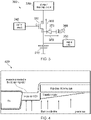
- Fig. 4 shows an example of a pass device 400 comprised in a storage device of the kind set forth.
- Fig. 4 shows the cross-sectional view of the pass device presented in schematic form in Fig. 1 . More specifically, it shown that in a situation in which the tag is unpowered, the gate voltage of the pass device is 0V and the storage voltage in the capacitor is 0.5V. Since the gate voltage of the pass device is 0V, a depletion region is formed under the gate. Once the tag is exposed to light, the depletion region contributes to increasing the electron collection area, causing an increased photocurrent and a decreased persistence time.
- the presently disclosed storage device and corresponding production method facilitate avoiding that a storage capacitor included in the storage device discharges too quickly when the storage device is exposed to light.
- a storage device comprising a capacitor configured to be charged, a charge circuit configured to charge said capacitor, a pass device coupled between the charge circuit and the capacitor, and a control circuit configured to control said pass device. Furthermore, the storage device comprises a photosensitive diode coupled between the control circuit and the pass device, such that an input voltage provided by the control circuit to the pass device is reduced if the storage device is exposed to light. By including the photosensitive diode, it may be avoided that the capacitor discharges too quickly when the storage device is exposed to light. This, in turn, facilitates maintaining the persistence time at an acceptable level.
- the pass device comprises a drain coupled to the charge circuit, a source coupled to the capacitor, and a gate coupled to the control circuit, and the input voltage is the gate voltage of the pass device.
- the input voltage is the gate voltage of the pass device.
- reducing the input voltage causes a layer of holes to be created around the source.
- said layer may be an accumulation layer. This further facilitates avoiding that the capacitor discharges too quickly when the storage device is exposed to light.
- the photosensitive diode contains a cathode terminal which is implemented as an n-well region connected to the gate and an anode terminal implemented as a p-substrate.
- the p-substrate may be a p-substrate of a transponder in which the storage device is included, such that a p-substrate that is already available may be reused for the purpose of reducing the light sensitivity of the storage device.
- the storage device comprises an output circuit coupled between the pass device and the capacitor, wherein the output circuit is configured to output a voltage present on the capacitor.
- the stored charge may easily be measurement and compared with the threshold, to output a value corresponding to, for example, a charged state or a discharged state.
- the charging state (i.e. charged or discharged) of the capacitor may represent information to be retained, in particular a bit.
- the measurement function and comparison function of the output circuit may be implemented in a conventional manner.
- Fig. 5 shows an illustrative embodiment of a storage device 500.
- Fig. 5 shows an example of an implementation of a storage device having a reduced sensitivity to light.
- the storage device 500 is implemented as a persistent flag, having a diode 591 placed at the gate of the pass device 520.
- One possible, non-limiting way to implement the diode is to connect the gate to an n-well region in such a way that the cathode terminal of the diode is the n-well region itself, while the anode terminal of the diode is the p-substrate of the tag.
- the n-well region of the diode can collect photo-generated electrons 593 and consequently a current flow 592 is created in order to pull the gate terminal of the pass device 520 negative.
- Fig. 6 shows an illustrative embodiment of a pass device 600 comprised in a storage device in accordance with the present disclosure.
- Fig. 6 illustrates a cross-sectional view of the pass device presented in schematic form in Fig. 5 . More specifically, it is shown that in a situation in which the tag is unpowered, the gate voltage of the pass device is -0.7V and the storage voltage in the capacitor is 0.5V. Since the gate voltage of the pass device is -0.7V, the depletion region present in the situation illustrated in Fig. 4 disappears, and an accumulation layer of holes is created around the source terminal of the pass device. Once the tag is exposed to light, the accumulation layer contributes to increasing the recombination electron-holes around the source terminal of the pass device, causing a decreased photocurrent and an increased persistence time.
- the presently disclosed storage device may have the following advantage.
- the magnitude of the photocurrent of the p-n junction associated with the source terminal of the pass device may be reduced, by decreasing the gate voltage of the pass device at light conditions, reducing therefore the light sensitivity of the persistence time.
- the insertion of a photosensitive diode at the gate of the pass device of a persistent flag decreases the gate voltage (i.e. pulls it below GND) of the pass device at light conditions, reducing in this way the light sensitivity of the persistence time.
Landscapes
- Engineering & Computer Science (AREA)
- Computer Hardware Design (AREA)
- Microelectronics & Electronic Packaging (AREA)
- Physics & Mathematics (AREA)
- General Physics & Mathematics (AREA)
- Theoretical Computer Science (AREA)
- Electromagnetism (AREA)
- Power Engineering (AREA)
- Charge And Discharge Circuits For Batteries Or The Like (AREA)
- Electronic Switches (AREA)
Abstract
Description
- The present disclosure relates to a storage device. Furthermore, the present disclosure relates to a corresponding method of producing a storage device.
- Storage devices based on the principle of maintaining a predefined charge on a capacitor are widely used. For instance, such storage devices may be used as so-called persistent flags in transponders. Nowadays, radio frequency identification (RFID) transponders are widely used, in different areas of industry and commerce and for various purposes. RFID transponders may for example be embodied as so-called RFID tags or RFID cards. It is noted that, in the present disclosure, near field communication (NFC) transponders are regarded as a specific type of RFID transponders. Thus, the principles described herein may also be applied to NFC transponders.
- In accordance with a first aspect of the present disclosure, a storage device is provided, comprising: a capacitor configured to be charged; a charge circuit configured to charge said capacitor; a pass device coupled between the charge circuit and the capacitor; a control circuit configured to control said pass device; a photosensitive diode coupled between the control circuit and the pass device, such that an input voltage provided by the control circuit to the pass device is reduced if the storage device is exposed to light.
- In one or more embodiments, the pass device comprises a drain coupled to the charge circuit, a source coupled to the capacitor, and a gate coupled to the control circuit, and said input voltage is the gate voltage of the pass device.
- In one or more embodiments, reducing the input voltage causes a layer of holes to be created around the source.
- In one or more embodiments, the photosensitive diode contains a cathode terminal which is implemented as an n-well region connected to the gate and an anode terminal implemented as a p-substrate.
- In one or more embodiments, the p-substrate is a p-substrate of a transponder in which the storage device is included.
- In one or more embodiments, the transponder is a radio frequency identification transponder or a near field communication transponder.
- In one or more embodiments, the device further comprises an output circuit coupled between the pass device and the capacitor, wherein the output circuit is configured to output a voltage present on the capacitor.
- In one or more embodiments, a charging state of the capacitor represents information to be retained, in particular a bit.
- In one or more embodiments, a transponder, in particular a radio frequency identification transponder or a near field communication transponder, comprises a storage device of the kind set forth.
- In accordance with a second aspect of the present disclosure, a method of producing a storage device is conceived, the method comprising providing the storage device with: a capacitor configured to be charged; a charge circuit configured to charge said capacitor; a pass device coupled between the charge circuit and the capacitor; a control circuit configured to control said pass device; a photosensitive diode coupled between the control circuit and the pass device, such that an input voltage provided by the control circuit to the pass device is reduced if the storage device is exposed to light.
- In one or more embodiments, the pass device comprises a drain coupled to the charge circuit, a source coupled to the capacitor, and a gate coupled to the control circuit, and said input voltage is the gate voltage of the pass device.
- In one or more embodiments, reducing the input voltage causes a layer of holes to be created around the source.
- In one or more embodiments, the photosensitive diode contains a cathode terminal which is implemented as an n-well region connected to the gate and an anode terminal implemented as a p-substrate.
- In one or more embodiments, the p-substrate is a p-substrate of a transponder in which the storage device is included.
- In one or more embodiments, the transponder is a radio frequency identification transponder or a near field communication transponder.
- Embodiments will be described in more detail with reference to the appended drawings, in which:
-
Fig. 1 shows an example of a storage device; -
Fig. 2 shows an example of a persistence time associated with a storage device; -
Fig. 3 shows another example of a storage device; -
Fig. 4 shows an example of a pass device comprised in a storage device; -
Fig. 5 shows an illustrative embodiment of a storage device; -
Fig. 6 shows an illustrative embodiment of a pass device comprised in a storage device. - As mentioned above, storage devices based on the principle of maintaining a predefined charge on a capacitor are widely used. For instance, such storage devices may be used as so-called persistent flags in transponders. Nowadays, radio frequency identification (RFID) transponders are widely used, in different areas of industry and commerce and for various purposes. RFID transponders may for example be embodied as so-called RFID tags or RFID cards. It is noted that, in the present disclosure, near field communication (NFC) transponders are regarded as a specific type of RFID transponders. Thus, the principles described herein may also be applied to NFC transponders.
- Persistent flags are a feature related to the RFID technology. The persistent flags have the function to retain the inventory state information of a transponder for a predetermined or predefined time. This predetermined time is often referred to as the persistence time. The function and the time requirements of each persistent flag are specified in a protocol, which is an industry standard defining the communication between a reader and a transponder, and vice versa. Such a protocol is for example defined in the document EPC™ Radio-Frequency Identity Protocols Generation-2 UHF RFID, version 2.0.1, published in April 2015. It is noted that reference is made to a tag in the examples and embodiments described herein. However, the presently disclosed storage device may also be used in other types of transponders or other devices.
-
Fig. 1 shows an example of astorage device 100. In particular,Fig. 1 shows a possible implementation of a persistent flag, such as described inUS 8,803,592 B2 . The implementation is formed by a capacitor 110, apass device 120, a charge/discharge circuit 130, acontrol circuit 140 and anoutput circuit 150. During the normal operation of a tag, in other words, when the tag is powered, the persistence flag can be set or reset. The set operation is performed by charging the capacitor 110 by enabling control through both thecharge circuit 130 and thecontrol circuit 140. The resulting charged voltage across the capacitor 110 is defined by the voltage applied at the gate and drain terminals of thepass device 120 and the threshold voltage of thepass device 120. The persistence time, which is associated with the charged voltage across the capacitor 110, is counted from the time when the tag becomes unpowered to the time when the voltage across the capacitor 110 falls below the threshold of a comparison function of theoutput circuit 150. -
Fig. 2 shows an example of apersistence time 200 associated with thestorage device 100 shown inFig. 1 . In particular, the time diagram shows that at t0 the tag becomes unpowered 210 and that consequently the voltage across the previously charged capacitor starts to decrease 220. At t1, the voltage across the capacitor falls below thethreshold 230 of the comparison function of the output circuit. The persistence time is defined as the difference t1 - t0. The parameters which influence the persistence time are the charge in the capacitor and the leakage current connected to the capacitor. In the circuit implementation illustrated inFig. 1 , the dominant current leakage source is the channel leakage of the pass device, which is an NMOS pass device. - Storage devices of the kind set form may be sensitive to light. For instance, it has been reported in
US 9,218,519 B2 -
Fig. 3 shows another example of astorage device 300. In particular, astorage device 300 is shown whose persistence time is affected bylight 390. Thestorage device 300 is implemented as a persistent flag, having ap-n junction 370 associated with the source terminal of thepass device 320. Since the tag is exposed to the light 390, an additional current flow, here denoted asphotocurrent 380, is created through the p-n junction at the source terminal of thepass device 320. Depending on the light intensity, the photocurrent could be the dominant one once compared with theleakage 360 of the pass device, and therefore, it would reduce the charge on the storage capacitor 310 rapidly, resulting in a decreased persistence time. -
Fig. 4 shows an example of apass device 400 comprised in a storage device of the kind set forth. In particular,Fig. 4 shows the cross-sectional view of the pass device presented in schematic form inFig. 1 . More specifically, it shown that in a situation in which the tag is unpowered, the gate voltage of the pass device is 0V and the storage voltage in the capacitor is 0.5V. Since the gate voltage of the pass device is 0V, a depletion region is formed under the gate. Once the tag is exposed to light, the depletion region contributes to increasing the electron collection area, causing an increased photocurrent and a decreased persistence time. - Now discussed are a storage device and a corresponding method of producing a storage device, which facilitate maintaining the persistence time at an acceptable level. In particular, the presently disclosed storage device and corresponding production method facilitate avoiding that a storage capacitor included in the storage device discharges too quickly when the storage device is exposed to light.
- According to a first aspect of the present disclosure, a storage device is provided. The storage device comprises a capacitor configured to be charged, a charge circuit configured to charge said capacitor, a pass device coupled between the charge circuit and the capacitor, and a control circuit configured to control said pass device. Furthermore, the storage device comprises a photosensitive diode coupled between the control circuit and the pass device, such that an input voltage provided by the control circuit to the pass device is reduced if the storage device is exposed to light. By including the photosensitive diode, it may be avoided that the capacitor discharges too quickly when the storage device is exposed to light. This, in turn, facilitates maintaining the persistence time at an acceptable level.
- In one or more embodiments, the pass device comprises a drain coupled to the charge circuit, a source coupled to the capacitor, and a gate coupled to the control circuit, and the input voltage is the gate voltage of the pass device. This results in a practical implementation of a storage device, whose persistence time less is affected by light. Furthermore, in one or more embodiments, reducing the input voltage causes a layer of holes to be created around the source. For instance, said layer may be an accumulation layer. This further facilitates avoiding that the capacitor discharges too quickly when the storage device is exposed to light. In a particularly efficient implementation, the photosensitive diode contains a cathode terminal which is implemented as an n-well region connected to the gate and an anode terminal implemented as a p-substrate. Furthermore, the p-substrate may be a p-substrate of a transponder in which the storage device is included, such that a p-substrate that is already available may be reused for the purpose of reducing the light sensitivity of the storage device.
- In one or more embodiments, the storage device comprises an output circuit coupled between the pass device and the capacitor, wherein the output circuit is configured to output a voltage present on the capacitor. In this way, the stored charge may easily be measurement and compared with the threshold, to output a value corresponding to, for example, a charged state or a discharged state. Accordingly, the charging state (i.e. charged or discharged) of the capacitor may represent information to be retained, in particular a bit. It is noted that the measurement function and comparison function of the output circuit may be implemented in a conventional manner.
-
Fig. 5 shows an illustrative embodiment of astorage device 500. In particular,Fig. 5 shows an example of an implementation of a storage device having a reduced sensitivity to light. Thestorage device 500 is implemented as a persistent flag, having adiode 591 placed at the gate of thepass device 520. One possible, non-limiting way to implement the diode, is to connect the gate to an n-well region in such a way that the cathode terminal of the diode is the n-well region itself, while the anode terminal of the diode is the p-substrate of the tag. The n-well region of the diode can collect photo-generatedelectrons 593 and consequently acurrent flow 592 is created in order to pull the gate terminal of thepass device 520 negative. -
Fig. 6 shows an illustrative embodiment of a pass device 600 comprised in a storage device in accordance with the present disclosure. In particular,Fig. 6 illustrates a cross-sectional view of the pass device presented in schematic form inFig. 5 . More specifically, it is shown that in a situation in which the tag is unpowered, the gate voltage of the pass device is -0.7V and the storage voltage in the capacitor is 0.5V. Since the gate voltage of the pass device is -0.7V, the depletion region present in the situation illustrated inFig. 4 disappears, and an accumulation layer of holes is created around the source terminal of the pass device. Once the tag is exposed to light, the accumulation layer contributes to increasing the recombination electron-holes around the source terminal of the pass device, causing a decreased photocurrent and an increased persistence time. - Thus, the presently disclosed storage device may have the following advantage. The magnitude of the photocurrent of the p-n junction associated with the source terminal of the pass device may be reduced, by decreasing the gate voltage of the pass device at light conditions, reducing therefore the light sensitivity of the persistence time. In a practical implementation, the insertion of a photosensitive diode at the gate of the pass device of a persistent flag decreases the gate voltage (i.e. pulls it below GND) of the pass device at light conditions, reducing in this way the light sensitivity of the persistence time.
- It is noted that the embodiments above have been described with reference to different subject-matters. In particular, some embodiments may have been described with reference to method-type claims whereas other embodiments may have been described with reference to apparatus-type claims. However, a person skilled in the art will gather from the above that, unless otherwise indicated, in addition to any combination of features belonging to one type of subject-matter also any combination of features relating to different subject-matters, in particular a combination of features of the method-type claims and features of the apparatus-type claims, is considered to be disclosed with this document.
- Furthermore, it is noted that the drawings are schematic. In different drawings, similar or identical elements are provided with the same reference signs. Furthermore, it is noted that in an effort to provide a concise description of the illustrative embodiments, implementation details which fall into the customary practice of the skilled person may not have been described. It should be appreciated that in the development of any such implementation, as in any engineering or design project, numerous implementation-specific decisions must be made in order to achieve the developers' specific goals, such as compliance with system-related and business-related constraints, which may vary from one implementation to another. Moreover, it should be appreciated that such a development effort might be complex and time consuming, but would nevertheless be a routine undertaking of design, fabrication, and manufacture for those of ordinary skill.
- Finally, it is noted that the skilled person will be able to design many alternative embodiments without departing from the scope of the appended claims. In the claims, any reference sign placed between parentheses shall not be construed as limiting the claim. The word "comprise(s)" or "comprising" does not exclude the presence of elements or steps other than those listed in a claim. The word "a" or "an" preceding an element does not exclude the presence of a plurality of such elements. Measures recited in the claims may be implemented by means of hardware comprising several distinct elements and/or by means of a suitably programmed processor. In a device claim enumerating several means, several of these means may be embodied by one and the same item of hardware. The mere fact that certain measures are recited in mutually different dependent claims does not indicate that a combination of these measures cannot be used to advantage.
-
- 100
- storage device
- 110
- capacitor
- 120
- pass device
- 130
- charge/discharge circuit
- 140
- control circuit
- 150
- output circuit
- 160
- channel leakage of the pass device
- 200
- persistence time
- 210
- input power
- 220
- voltage across the capacitor
- 230
- threshold of the output circuit
- 300
- storage device
- 310
- capacitor
- 320
- pass device
- 330
- charge/discharge circuit
- 340
- control circuit
- 350
- output circuit
- 360
- channel leakage of the pass device
- 370
- p-n junction
- 380
- photocurrent
- 390
- light
- 400
- cross-sectional view of the pass device
- 500
- storage device
- 510
- capacitor
- 520
- pass device
- 530
- charge/discharge circuit
- 540
- control circuit
- 550
- output circuit
- 560
- channel leakage of the pass device
- 570
- p-n junction
- 580
- photocurrent
- 590
- light
- 591
- photosensitive diode
- 592
- current flow
- 593
- photo-generated electrons
- 600
- cross-sectional view of the pass device
Claims (15)
- A storage device, comprising:- a capacitor configured to be charged;- a charge circuit configured to charge said capacitor;- a pass device coupled between the charge circuit and the capacitor;- a control circuit configured to control said pass device;- a photosensitive diode coupled between the control circuit and the pass device, such that an input voltage provided by the control circuit to the pass device is reduced if the storage device is exposed to light.
- The device of claim 1, wherein the pass device comprises a drain coupled to the charge circuit, a source coupled to the capacitor, and a gate coupled to the control circuit, and wherein said input voltage is the gate voltage of the pass device.
- The device of claim 2, wherein reducing the input voltage causes a layer of holes to be created around the source.
- The device of claim 2 or 3, wherein the photosensitive diode contains a cathode terminal which is implemented as an n-well region connected to the gate and an anode terminal implemented as a p-substrate.
- The device of claim 4, wherein the p-substrate is a p-substrate of a transponder in which the storage device is included.
- The device of claim 5, wherein the transponder is a radio frequency identification transponder or a near field communication transponder.
- The device of any preceding claim, further comprising an output circuit coupled between the pass device and the capacitor, wherein the output circuit is configured to output a voltage present on the capacitor.
- The device of any preceding claim, wherein a charging state of the capacitor represents information to be retained, in particular a bit.
- A transponder, in particular a radio frequency identification transponder or a near field communication transponder, comprising the storage device of any preceding claim.
- A method of producing a storage device, the method comprising providing the storage device with:- a capacitor configured to be charged;- a charge circuit configured to charge said capacitor;- a pass device coupled between the charge circuit and the capacitor;- a control circuit configured to control said pass device;- a photosensitive diode coupled between the control circuit and the pass device, such that an input voltage provided by the control circuit to the pass device is reduced if the storage device is exposed to light.
- The method of claim 10, wherein the pass device comprises a drain coupled to the charge circuit, a source coupled to the capacitor, and a gate coupled to the control circuit, and wherein said input voltage is the gate voltage of the pass device.
- The method of claim 11, wherein reducing the input voltage causes a layer of holes to be created around the source.
- The method of claim 11 or 12, wherein the photosensitive diode contains a cathode terminal which is implemented as an n-well region connected to the gate and an anode terminal implemented as a p-substrate.
- The method of claim 13, wherein the p-substrate is a p-substrate of a transponder in which the storage device is included.
- The method of claim 14, wherein the transponder is a radio frequency identification transponder or a near field communication transponder.
Priority Applications (3)
| Application Number | Priority Date | Filing Date | Title |
|---|---|---|---|
| EP21183406.4A EP4113520A1 (en) | 2021-07-02 | 2021-07-02 | Storage device and method of producing the same |
| CN202210720410.8A CN115566749A (en) | 2021-07-02 | 2022-06-16 | Memory device and method for generating the same |
| US17/808,125 US11922244B2 (en) | 2021-07-02 | 2022-06-22 | Storage device and method of producing the same |
Applications Claiming Priority (1)
| Application Number | Priority Date | Filing Date | Title |
|---|---|---|---|
| EP21183406.4A EP4113520A1 (en) | 2021-07-02 | 2021-07-02 | Storage device and method of producing the same |
Publications (1)
| Publication Number | Publication Date |
|---|---|
| EP4113520A1 true EP4113520A1 (en) | 2023-01-04 |
Family
ID=76764887
Family Applications (1)
| Application Number | Title | Priority Date | Filing Date |
|---|---|---|---|
| EP21183406.4A Pending EP4113520A1 (en) | 2021-07-02 | 2021-07-02 | Storage device and method of producing the same |
Country Status (3)
| Country | Link |
|---|---|
| US (1) | US11922244B2 (en) |
| EP (1) | EP4113520A1 (en) |
| CN (1) | CN115566749A (en) |
Citations (4)
| Publication number | Priority date | Publication date | Assignee | Title |
|---|---|---|---|---|
| WO1999030368A1 (en) * | 1997-12-08 | 1999-06-17 | Intel Corporation | High sensitivity active pixel with electronic shutter |
| US8803592B2 (en) | 2012-07-26 | 2014-08-12 | Lsis Co., Ltd. | Data persistence control apparatus for RFID tag |
| US9218519B2 (en) | 2008-04-07 | 2015-12-22 | Alien Technology Corporation | Subset selection of RFID tags using light |
| US20200346004A1 (en) * | 2017-10-25 | 2020-11-05 | École Centrale De Lille | Optical sensor |
Family Cites Families (7)
| Publication number | Priority date | Publication date | Assignee | Title |
|---|---|---|---|---|
| US3703669A (en) | 1971-08-12 | 1972-11-21 | Motorola Inc | Photocurrent cross talk isolation |
| US4876583A (en) | 1988-03-21 | 1989-10-24 | The United States Of America As Represented By The Secretary Of The Air Force | Radiation-induced substrate photo-current compensation apparatus |
| US6021063A (en) | 1997-01-13 | 2000-02-01 | Vanguard International Semiconductor Corporation | Method and structure for improving data retention in a DRAM |
| US6369426B2 (en) | 2000-04-27 | 2002-04-09 | Infineon Technologies North America Corp. | Transistor with integrated photodetector for conductivity modulation |
| TWI595637B (en) * | 2012-09-28 | 2017-08-11 | 新力股份有限公司 | Semiconductor devices and electronic devices |
| US20150221363A1 (en) | 2013-04-03 | 2015-08-06 | Goran Krilic | Method for cache sram data retention in switched off power supply mode generating extremely small power dissipation |
| US9755701B2 (en) * | 2015-03-31 | 2017-09-05 | International Business Machines Corporation | Hybrid tag for radio frequency identification system |
-
2021
- 2021-07-02 EP EP21183406.4A patent/EP4113520A1/en active Pending
-
2022
- 2022-06-16 CN CN202210720410.8A patent/CN115566749A/en active Pending
- 2022-06-22 US US17/808,125 patent/US11922244B2/en active Active
Patent Citations (4)
| Publication number | Priority date | Publication date | Assignee | Title |
|---|---|---|---|---|
| WO1999030368A1 (en) * | 1997-12-08 | 1999-06-17 | Intel Corporation | High sensitivity active pixel with electronic shutter |
| US9218519B2 (en) | 2008-04-07 | 2015-12-22 | Alien Technology Corporation | Subset selection of RFID tags using light |
| US8803592B2 (en) | 2012-07-26 | 2014-08-12 | Lsis Co., Ltd. | Data persistence control apparatus for RFID tag |
| US20200346004A1 (en) * | 2017-10-25 | 2020-11-05 | École Centrale De Lille | Optical sensor |
Also Published As
| Publication number | Publication date |
|---|---|
| US11922244B2 (en) | 2024-03-05 |
| CN115566749A (en) | 2023-01-03 |
| US20230004770A1 (en) | 2023-01-05 |
Similar Documents
| Publication | Publication Date | Title |
|---|---|---|
| CN102057383B (en) | Subset selection of RFID tags using light | |
| US6963269B2 (en) | Contactless IC card | |
| Yao et al. | A–$21.2 $-dBm dual-channel UHF passive CMOS RFID Tag design | |
| US20170244405A1 (en) | Power switching circuit | |
| KR101849000B1 (en) | Auxiliary charge pump for a rectifier of an rfid transponder | |
| US20090219079A1 (en) | Charge pump circuit for rfid integrated circuits | |
| US11922244B2 (en) | Storage device and method of producing the same | |
| US12476484B2 (en) | Energy harvesting unit and operating method thereof | |
| CN106026722B (en) | A kind of rectification circuit and the superfrequency label with the rectification circuit | |
| JP6347179B2 (en) | Semiconductor device | |
| JP2000299440A (en) | Field effect transistor and integrated voltage generation circuit using the same | |
| US11270177B2 (en) | RFID transponder and corresponding operating method | |
| EP1516363B1 (en) | Data carrier comprising an integrated circuit with an esd protection circuit | |
| US8159844B2 (en) | Full-wave rectifying device | |
| EP3742341A1 (en) | Rfid transponder and method of operating the same | |
| JP2002152080A (en) | Tag and semiconductor integrated circuit used therefor | |
| EP3905136A1 (en) | Rfid transponder and method of operating an rfid transponder | |
| US20250190736A1 (en) | Front-end circuit for an rfid transponder | |
| JPWO2007148401A1 (en) | Rectifier circuit and wireless communication device using the same | |
| CN100416831C (en) | Semiconductor devices, full-wave rectification circuits, and half-wave rectification circuits | |
| US11126906B2 (en) | Transponder and corresponding operating method | |
| CN110176266B (en) | NVM (non-volatile memory) quick coding system of ultrahigh frequency radio frequency chip |
Legal Events
| Date | Code | Title | Description |
|---|---|---|---|
| PUAI | Public reference made under article 153(3) epc to a published international application that has entered the european phase |
Free format text: ORIGINAL CODE: 0009012 |
|
| STAA | Information on the status of an ep patent application or granted ep patent |
Free format text: STATUS: THE APPLICATION HAS BEEN PUBLISHED |
|
| AK | Designated contracting states |
Kind code of ref document: A1 Designated state(s): AL AT BE BG CH CY CZ DE DK EE ES FI FR GB GR HR HU IE IS IT LI LT LU LV MC MK MT NL NO PL PT RO RS SE SI SK SM TR |
|
| STAA | Information on the status of an ep patent application or granted ep patent |
Free format text: STATUS: REQUEST FOR EXAMINATION WAS MADE |
|
| 17P | Request for examination filed |
Effective date: 20230704 |
|
| RBV | Designated contracting states (corrected) |
Designated state(s): AL AT BE BG CH CY CZ DE DK EE ES FI FR GB GR HR HU IE IS IT LI LT LU LV MC MK MT NL NO PL PT RO RS SE SI SK SM TR |