EP4109759A1 - Error-feedback sar adc - Google Patents
Error-feedback sar adc Download PDFInfo
- Publication number
- EP4109759A1 EP4109759A1 EP22178462.2A EP22178462A EP4109759A1 EP 4109759 A1 EP4109759 A1 EP 4109759A1 EP 22178462 A EP22178462 A EP 22178462A EP 4109759 A1 EP4109759 A1 EP 4109759A1
- Authority
- EP
- European Patent Office
- Prior art keywords
- capacitor
- analog
- adc
- input sampling
- gain
- Prior art date
- Legal status (The legal status is an assumption and is not a legal conclusion. Google has not performed a legal analysis and makes no representation as to the accuracy of the status listed.)
- Pending
Links
Images






Classifications
-
- H—ELECTRICITY
- H03—ELECTRONIC CIRCUITRY
- H03M—CODING; DECODING; CODE CONVERSION IN GENERAL
- H03M1/00—Analogue/digital conversion; Digital/analogue conversion
- H03M1/06—Continuously compensating for, or preventing, undesired influence of physical parameters
- H03M1/08—Continuously compensating for, or preventing, undesired influence of physical parameters of noise
- H03M1/0854—Continuously compensating for, or preventing, undesired influence of physical parameters of noise of quantisation noise
-
- H—ELECTRICITY
- H03—ELECTRONIC CIRCUITRY
- H03M—CODING; DECODING; CODE CONVERSION IN GENERAL
- H03M1/00—Analogue/digital conversion; Digital/analogue conversion
- H03M1/06—Continuously compensating for, or preventing, undesired influence of physical parameters
- H03M1/0617—Continuously compensating for, or preventing, undesired influence of physical parameters characterised by the use of methods or means not specific to a particular type of detrimental influence
- H03M1/0626—Continuously compensating for, or preventing, undesired influence of physical parameters characterised by the use of methods or means not specific to a particular type of detrimental influence by filtering
-
- H—ELECTRICITY
- H03—ELECTRONIC CIRCUITRY
- H03M—CODING; DECODING; CODE CONVERSION IN GENERAL
- H03M1/00—Analogue/digital conversion; Digital/analogue conversion
- H03M1/002—Provisions or arrangements for saving power, e.g. by allowing a sleep mode, using lower supply voltage for downstream stages, using multiple clock domains or by selectively turning on stages when needed
-
- H—ELECTRICITY
- H03—ELECTRONIC CIRCUITRY
- H03M—CODING; DECODING; CODE CONVERSION IN GENERAL
- H03M1/00—Analogue/digital conversion; Digital/analogue conversion
- H03M1/10—Calibration or testing
- H03M1/1009—Calibration
-
- H—ELECTRICITY
- H03—ELECTRONIC CIRCUITRY
- H03M—CODING; DECODING; CODE CONVERSION IN GENERAL
- H03M3/00—Conversion of analogue values to or from differential modulation
- H03M3/30—Delta-sigma modulation
- H03M3/39—Structural details of delta-sigma modulators, e.g. incremental delta-sigma modulators
- H03M3/412—Structural details of delta-sigma modulators, e.g. incremental delta-sigma modulators characterised by the number of quantisers and their type and resolution
- H03M3/422—Structural details of delta-sigma modulators, e.g. incremental delta-sigma modulators characterised by the number of quantisers and their type and resolution having one quantiser only
- H03M3/424—Structural details of delta-sigma modulators, e.g. incremental delta-sigma modulators characterised by the number of quantisers and their type and resolution having one quantiser only the quantiser being a multiple bit one
- H03M3/426—Structural details of delta-sigma modulators, e.g. incremental delta-sigma modulators characterised by the number of quantisers and their type and resolution having one quantiser only the quantiser being a multiple bit one the quantiser being a successive approximation type analogue/digital converter
-
- H—ELECTRICITY
- H03—ELECTRONIC CIRCUITRY
- H03M—CODING; DECODING; CODE CONVERSION IN GENERAL
- H03M1/00—Analogue/digital conversion; Digital/analogue conversion
- H03M1/10—Calibration or testing
- H03M1/1009—Calibration
- H03M1/1033—Calibration over the full range of the converter, e.g. for correcting differential non-linearity
- H03M1/1057—Calibration over the full range of the converter, e.g. for correcting differential non-linearity by trimming, i.e. by individually adjusting at least part of the quantisation value generators or stages to their nominal values
- H03M1/1061—Calibration over the full range of the converter, e.g. for correcting differential non-linearity by trimming, i.e. by individually adjusting at least part of the quantisation value generators or stages to their nominal values using digitally programmable trimming circuits
-
- H—ELECTRICITY
- H03—ELECTRONIC CIRCUITRY
- H03M—CODING; DECODING; CODE CONVERSION IN GENERAL
- H03M1/00—Analogue/digital conversion; Digital/analogue conversion
- H03M1/12—Analogue/digital converters
- H03M1/34—Analogue value compared with reference values
- H03M1/38—Analogue value compared with reference values sequentially only, e.g. successive approximation type
- H03M1/46—Analogue value compared with reference values sequentially only, e.g. successive approximation type with digital/analogue converter for supplying reference values to converter
- H03M1/466—Analogue value compared with reference values sequentially only, e.g. successive approximation type with digital/analogue converter for supplying reference values to converter using switched capacitors
-
- H—ELECTRICITY
- H03—ELECTRONIC CIRCUITRY
- H03M—CODING; DECODING; CODE CONVERSION IN GENERAL
- H03M3/00—Conversion of analogue values to or from differential modulation
- H03M3/30—Delta-sigma modulation
- H03M3/458—Analogue/digital converters using delta-sigma modulation as an intermediate step
Definitions
- This invention relates to analog to digital conversion circuitry.
- Noise-shaping successive-approximation-register analog to digital converters achieve high accuracy with good power efficiency by introducing concepts from sigma-delta ( ⁇ ) ADCs into SAR-ADCs. They do this by taking the residue voltage, left on the top plates of the capacitor digital-to-analog converter (CDAC) after each bit-cycling conversion, and feeding the residue into a filter which then subtracts it from the next analog sample.
- One structure that can be used to implement such noise-shaping is an error-feedback structure, in which the residue voltage is fed back to the input of the SAR-ADC and is subtracted from the next sample at the input.
- the residue voltage represents a combination of the different noise sources present in the ADC, such as quantization noise and comparator noise.
- quantization noise and comparator noise By performing this residue subtraction operation over a series of consecutive samples, low-frequency noise can be suppressed, at the cost of increased high-frequency noise.
- a decimation filter By oversampling the input, a decimation filter can then be applied at the output of the SAR-ADC to remove the high-frequency noise, resulting in an improvement in accuracy over a similar SAR-ADC without noise-shaping.
- Embodiments of the present invention seek to provide a more efficient design of error-feedback SAR-ADC conversion circuitry.
- analog to digital conversion circuitry comprising:
- the invention provides an analog to digital conversion method, comprising:
- the same gain-control capacitor is used both as a feedback capacitor for the amplifier (to determine the gain applied to the sampled analog signal) and also for receiving a residue voltage from the SAR-ADC.
- the residue voltage can thus be conveniently used to affect the level of the subsequent sample-e.g. by being subtracted from the input signal-without having to provide a dedicated separate residue buffer, comprising one or more additional capacitors, in addition to the capacitors in the input sampling buffer, and without requiring a second amplifier for transferring the residue voltage.
- Embodiments can therefore be particularly efficient both in area and power consumption.
- the analog to digital conversion circuitry is preferably arranged to provide error-feedback noise-shaping. It may be configured to oversample the input signal. It may comprise a decimation filter for down-sampling the digital signal generated by the SAR-ADC.
- noise-shaping in preferred embodiments can advantageously provide increased accuracy, albeit with lower effective bandwidth, without having to increase the area, and therefore the power consumption, e.g. when the ADC is implemented as an integrated circuit.
- the gain, determined by the gain-control capacitor may be positive or it may be negative (i.e. to attenuate the analog signal, if the supply input range is too large for the SAR-ADC).
- the gain-control capacitor may be of fixed or variable capacitance. The gain may be configurable.
- the analog to digital conversion circuitry may comprise a control interface for receiving control signals, e.g. from a processor or microcontroller.
- the successive-approximation-register analog to digital converter may be a differential converter. It may comprise respective positive and negative paths.
- the amplifier may be a differential amplifier.
- the input sampling buffer may comprise a pair of input sampling capacitors, which may be of the same nominal capacitance. It may comprise a pair of gain-control capacitors, which may be of the same nominal capacitance. These capacitor pairs may be provided on respective positive and negative paths of the differential converter.
- the amplifier may be an operational transconductance amplifier (OTA).
- OTA operational transconductance amplifier
- the input sampling buffer preferably comprises a set of one or more switches for switching between the amplification configuration (i.e. state, or mode of operation) and the error-feedback configuration (i.e. state, or mode of operation). It may comprise a plurality switches for selection of the amplification and error-feedback configurations. A first subset of the switches may be closed when operating in the amplification configuration and open when not in the amplification configuration. A second subset of the switches may be closed when operating in the error-feedback configuration and open when not in the error-feedback configuration.
- the input sampling buffer may thus be switched between the configurations (and any optional further configurations) by selectively opening and closing switches.
- the ADC circuitry may comprise control logic for controlling the switches.
- the control logic may comprise a hardware finite state machine.
- the control logic may be implemented in hardware (e.g. using dedicated sequential logic), or it may be implemented in software, or by a combination of hardware and software.
- the ADC circuitry may comprise a processor and a memory storing software for execution by the processor.
- the input sampling buffer may be configured to receive the analog signal onto the input sampling capacitor when in the error-feedback configuration.
- the input sampling buffer may have a sampling configuration, in which it is configured to receive the analog signal onto the input sampling capacitor, which may be distinct from the error-feedback configuration and/or from the amplification configuration.
- the ADC circuitry may control the input sampling buffer to cycle between the error-feedback configuration and the amplification configuration (optionally also passing through one or more further configurations) at a sampling rate. It may cycle once for each sample of a succession of samples provided to the SAR-ADC from the input sampling buffer.
- the residue voltage from one sample may influence the level of a subsequent-e.g. the next-sample provided to the SAR-ADC.
- the input sampling buffer may be arranged to subtract the residue voltage from the next sample-i.e. to provide the SAR-ADC with the difference between the residue voltage and the sample with nominal gain applied.
- the gain-control capacitor may be arranged to be connected in parallel with the amplifier when the input sampling buffer is in the amplification configuration.
- the input sampling buffer may comprise one or more dedicated-error-feedback capacitors, each arranged to be switchably connected in feedback with the amplifier (i.e. arranged to be switchably connected in parallel with the amplifier).
- Each dedicated-error-feedback capacitor may be switchable independently from the gain-control capacitor. This may, in some embodiments, allow the gain-control capacitor and one or more dedicated-error-feedback capacitors to be connected in feedback with the amplifier, when in the error-feedback configuration. This can allow the gain to be adjusted for different situations.
- the gain-control capacitor and the one or more dedicated-error-feedback capacitors may be connected in parallel with each other when in the error-feedback configuration. Switches may allow the dedicated-error-feedback capacitors to be decoupled (i.e.
- the feedback capacitance applied to the amplifier can be different in the two configurations. This may be useful e.g. for setting coefficients in the filter transfer function, when using a higher-order filter, through selectively attenuating the error-feedback voltage.
- the SAR-ADC preferably comprises a capacitor digital-to-analog converter (CDAC), which may be a differential CDAC.
- the ADC circuitry preferably comprises control logic for performing bit-cycling with CDAC.
- the residue voltage may be received from the top plates of the capacitors of the CDAC.
- a positive residue voltage component may be received from a positive side of the CDAC by a positive-side gain-control capacitor, in the error-feedback configuration, and a negative residue voltage component may be received from a negative side of the CDAC by a negative-side gain-control capacitor.
- the ADC circuitry may, in some embodiments, comprise calibration circuitry for performing a calibration of the SAR-ADC. It may be configured to calibrate each of a set of a capacitors of a CDAC of the SAR-ADC. It may calibrate a strict subset of the capacitors, which may be a succession of the most significant capacitors of the CDAC-i.e. a subset of capacitors of CDAC each having larger capacitance than any of the capacitors of the CDAC that are not in the subset.
- the calibration circuitry may be arranged to calibrate one capacitor or one differential capacitor pair at a time. It may calibrate the capacitors in order from largest to smallest.
- Such calibration may improve the linearity of the SAR-ADC.
- it may be advantageously implemented by digital control, without requiring any additional analog circuitry.
- the calibration circuitry may be arranged, when calibrating a capacitor (or capacitor pair), to switch capacitors of the CDAC so as to generate a residual voltage that is proportional to a mismatch between the capacitor being calibrated and one or more further capacitors of the CDAC. It may determine a mismatch between the capacitor under calibration and a set of other capacitors of total nominal capacitance equal to the capacitor under calibration.
- the ADC circuitry may support a calibration configuration (i.e. a calibration state or mode), in which the gain-control capacitor is decoupled from the input sampling capacitor and is arranged to receive a mismatch voltage from the SAR-ADC.
- a calibration configuration i.e. a calibration state or mode
- an error-feedback noise-shaping loop may be used to sample a residual mismatch voltage, which resides on the top plates of the CDAC after the switching.
- This efficient use of the input sampling buffer also for calibration can avoid the need for additional analog components and capacitors to provide calibration. Sampling the mismatch residue onto the gain-control (error-feedback) capacitor can also advantageously allow the SAR-ADC to be reset without the mismatch residue being deleted by the reset.
- the calibration circuitry may be arranged to convert the mismatch voltage with the SAR-ADC.
- the ADC circuitry may be configured to calculate calibration coefficients from digital measurements, output by the SAR-ADC, of the mismatches of a set of capacitors of the SAR-ADC. These coefficients may be used to increase linearity of the ADC in subsequent operation.
- the ADC circuitry may be configured to adjust the digital signal output by the SAR-ADC in dependence on one or more of the calibration coefficients-e.g. being configured to add or subtract one or more calibration coefficients from subsequent digital samples.
- the ADC conversion circuitry may be provided by an integrated-circuit device, such as a system-on-chip. It may be integrated as a peripheral to a processor, such as microcontroller. It have an input for receiving the analog signal and/or an output for outputting the digital signal.
- a processor such as microcontroller. It have an input for receiving the analog signal and/or an output for outputting the digital signal.
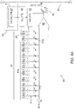
- Figure 1 shows the high-level architecture of an analog-to-digital converter (ADC) 1 circuit portion. It may, in some embodiments, be incorporated as a peripheral within an integrated-circuit system-on-chip (SoC), such as a digital radio on a chip, or it may be used in any other appropriate context.
- SoC integrated-circuit system-on-chip
- PADC peripheral ADC
- the ADC 1 has a programmable-gain switched-capacitor input sampling buffer 2, which is coupled to an SAR-ADC 3 for converting the samples sampled by the buffer 2.
- this ADC 1 enables first-order error-feedback noise-shaping, where the input sampling buffer 2 is reused as a loop filter.
- the SAR-ADC 3 comprises a differential capacitor digital-to-analog converter (CDAC) array 4 which feeds into a comparator 5. It also has a control block control logic, SAR_CTRL 6, and output circuitry 11.
- CDAC digital-to-analog converter
- the input sampling buffer 2 has positive and negative paths that can be coupled to an operational transconductance amplifier (OTA) 8 and capacitors C1, C1', C2, C2', through a set of switches, the operation of which is described below.
- OTA operational transconductance amplifier
- the switches are shown in simplified schematic form in Figure 2 , represented by six switches on each of the positive and negative sides, but a more detailed implementation using twenty-eight switches, labelled S1-S14, S1'-S14', is also shown in Figure 5 .
- the switches are controlled by the control block control logic, SAR_CTRL 6 or by a higher-level state machine.
- control logic controls the SAR-ADC 3 to convert a sample, sampled by the input buffer 2, in a conventional manner, by performing SAR bit-cycling with ten capacitors 7, "C512", “C256”, ..., “C4", "C2", “C1", of the CDAC 4.
- C represents one unit capacitance, so “C512” indicates 512 unit capacitors.
- the SAR_CTRL 6 then switches a respective pair of further capacitors 10, "C0.5", on each of the positive and negative sides, after the conversion, to get the residual voltage, by dividing the voltage after the least-significant-bit (LSB) decision in two.
- Each of the C0.5 capacitors 10 equals the C1 capacitors split in two; they do not suffer the same mismatch requirement as the rest of the CDAC 4.
- the SAR_CTRL 6 enables two feedback switches 9 ( ⁇ ErrorFB ) to switch the input sampling buffer 2 to an error-feedback configuration.
- the input sampling buffer 2 then transfers the residue voltage from the top plates of the CDAC 4 to a gain-control feedback capacitor C2 in the input sampling buffer 2, and to corresponding capacitor C2' on the negative side. (Note, these are different from the capacitors "C2" in the CDAC 4.)
- Figure 2 shows a close-up of the input sampling buffer 2.
- the next sample can be collected on the input sampling capacitors C1 and C1'. (Note, these are different from the capacitors "C1" in the CDAC 4.)
- Figure 3 provides a simplified schematic view of the input sampling buffer 2 still in the error-feedback configuration, showing the effect of the switches but omitting the switches themselves, to highlight how the next sample can be collected on C1 and C1', which are decoupled from the CDAC 4.
- the SAR_CTRL 6 operates the switches in the input sampling buffer 2 to set the buffer 2 to an amplification configuration, as shown in Figure 4 .
- Figure 4 provides a simplified schematic view of the input sampling buffer 2 in the amplification configuration (again showing the effect of the switches, but not the switches themselves).
- the next sample is transferred from the capacitors C1, C1' onto the CDAC 4, through the OTA 8.
- the gain-control feedback capacitors C2, C2' are also coupled between the inputs and outputs of the OTA 8 so as to remove the voltage residue stored on the capacitors C2, C2', obtained from the previous sample, thereby transferring the difference between the sampled input voltage and the residue voltage to the CDAC 4.
- error-feedback is applied to the new sample, as can be seen in the values of the voltages as shown in Figures 3 & 4 .
- the ADC 1 can be controlled to take a number, X, of samples, by performing the operations above to obtain each of these X samples.
- the result from each of the X samples is passed to a digital decimation filter, in the output circuitry 11, to filter out of band noise.
- the output of the decimation filter is one sample out per X samples in. This provides noise-shaping through oversampling and decimation.
- Figure 5 is more-detailed schematic diagram of the input sampling buffer 2.
- the capacitance C2 on each path may be implemented as two separate capacitors: a gain-control feedback capacitor C2a, which is used both for determining the gain applied to samples and as an error-feedback capacitor for capturing the residue voltage from the SADC, and a dedicated error-feedback capacitor C2b, which is used for capturing the residue in parallel with C2a.
- the capacitors C2a and C2b are of equal size. The provision of C2b in addition to C2a allows the gain to be adjusted. When transferring the residue voltage, both C2a and C2b are connected. When capturing the feedback, the capacitor C2b is either kept connected, together with C2a, or is disconnected, depending on a configurable gain setting.
- the total size of C2 is designed to match the total size of the CDAC 4, so as to get a gain of one in the transfer of the residue voltage.
- one or more further dedicated error-feedback capacitors, C2c, C2d, C2e, etc. may be provided similarly, and can be switchably coupled in parallel with C2a to provide further gain control.
- the role of the input sampling buffer 2 is to take the I/O supply input range and divide it down to a reasonable range for the SAR-ADC core 3.
- it has a configurable range of gain settings, from 2/3 (e.g. 1.8Vppd with a 1.2V reference) to 4 (e.g. 300mVppd with a 1.2V reference).
- the switches S11 and S14 may also be enabled in phase ⁇ 2 (i.e. in the input amplification phase) so that the feedback capacitor C2b is also connected, in parallel with the gain-control capacitor C2a, in the amplification configuration, in order to provide a desired gain for the ADC 1.
- the amplification gain during the amplification phase will then C1/(C2a+C2b).
- further switches can be operated to provide finer gain control.
- the error-feedback noise-shaping can be turned on and off through the control logic 6 (e.g. by a microcontroller).
- Figure 6 is a timing diagram for the buffering and conversion operations when error-feedback noise-shaping is enabled.
- Figure 7 is a timing diagram for the buffering and conversion operations when error-feedback noise-shaping is disabled.
- control logic SAR_CTRL 6 The following four signals are output from the control logic SAR_CTRL 6 or from a higher-level state machine, and are distributed to the blocks that need them as appropriate:
- the main FSM cycles through the same states whether or not noise-shaping is enabled.
- the switch phase ⁇ 3 is never activated.
- the bit-cycling FSM enters an Error feedback state, after the BitCycling state, which causes the switch phase ⁇ 3 to be active, as shown, causing the input sampling buffer 2 to enter the error-feedback configuration, described above.
- the switch phase ⁇ 4 is also different when noise-shaping is enabled, to capture the residue on the capacitors C2a and C2b when the feedback path is connected.
- FIG 8 shows another SAR-ADC 80, embodying the invention, that again provides error-feedback noise-shaping, but with additional features for performing linearity calibration.
- This ADC 80 has been designed with a custom CDAC 81 where the focus has been to reduce the amount of capacitance to a minimum to save power. The down side of this is higher mismatch and more noise. However, the error-feedback noise-shaping helps to mitigate the noise penalty. Noise-shaping may be used to reach very high accuracies on low frequencies. Linearity calibration is provided to achieve good linearity even in high accuracy modes. Linearity calibration enables the linearity to get to the same levels as noise where SNR (signal-to-noise ratio) ⁇ SFDR (spurious free dynamic range).
- FIG 8 shows a high-level architectural diagram of parts of the analog and digital portions of the ADC SAR core 80.
- the ADC 80 has an input sampling buffer (not shown in Figure 8 , although represented schematically in Figure 12 & 13 ), similar to the input sampling buffer 2 of Figure 1 above.
- This is connected to a differential CDAC 81 (only the positive side is shown in Figure 8 for simplicity, but there is also a similar negative side), and control logic SAR_CTRL 82, similar to the SAR_CTRL 6 described above.
- the ADC 80 also has higher-level digital logic output circuitry 83, comprising a calibration control logic block DIG_CAL_CTRL 87, for initiating and controlling the calibration procedure, by outputting appropriate control signals to the ADC 80, and for processing 12-bit digital output words received from a set of twelve flip flops 84 at the output of a comparator 85 of the CDAC 81.
- This circuitry 83 enables the capacitors to be measured in turn, and stores the results for further calculations.
- This digital control circuitry 83 may be implemented in hardware, as state machine implemented with dedicated logic gates, or it may be implemented at least partly by software executing on a processor of the device.
- a lower-level calibration control logic block CAL_CTRL 86 handles internal operations of the ADC 80 by controlling switching during the calibration switching procedure, under the higher-level control of the calibration control logic block DIG_CAL_CTRL 87.
- These two blocks 86, 87 are features 91 involved in the linearity calibration.
- This particular exemplary ADC 80 is intended as an 11-bit ADC, so the CDAC 81 has ten main capacitors 81a, labelled "C1" up to "C512", on each side, where C is one unit capacitance, and where 512C means 512 unit capacitors. C1 to C512 therefore form a 10-bit CDAC.
- this 11-bit ADC needs only a 10-bit CDAC 81 is that it implements a V CM -based (common-mode-voltage based) switching scheme, which removes the need for the most-significant-bit (MSB) capacitor that, in a conventional 11-bit SAR-ADC, would be weighted 1024C.
- V CM -based (common-mode-voltage based) switching scheme which removes the need for the most-significant-bit (MSB) capacitor that, in a conventional 11-bit SAR-ADC, would be weighted 1024C.
- the first capacitor 81b of a pair of 0.5C capacitors "C0.5", on the positive side, is provided to achieve noise-shaping as described above with reference to Figure 1 .
- This capacitor 81b is only switched when noise-shaping is activated to get the correct residue voltage to feed into the noise-shaping loop filter.
- the calibration procedure uses a switching scheme to provoke, and then convert, a residual voltage due to capacitor mismatch, and then implements an algorithm to use this converted residual to calculate calibration coefficients.
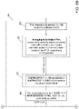
- Figures 9-14 illustrate the calibration procedure by showing states of the analog side of the ADC 80 during five main phases the procedure. These phases 1 to 5 are repeated X number of times to get X conversions of the residual voltage, for each capacitor that is to be calibrated.
- the top six most-significant capacitors, C512 to C16, are calibrated, while the five least-significant capacitors, C8, C4, C2, C1, C0.5, are used to convert any mismatch voltage, as explained below. Since the largest capacitors contribute most to the linearity of the ADC 80, it may be sufficient to leave the smallest capacitors uncalibrated.
- FIG. 9 shows "phase 1" of the calibration procedure, in which the inputs of the ADC 80 are shorted and a regular sample is taken with the ADC 80.
- the voltage VBUF_CM is the output common mode from the OTA, PADC_BUF 120 (see Figures 12 & 13 ), of the input sampling buffer of the ADC 80.
- the inputs of the input sampling buffer are shorted, so that both positive (P) and negative (N) sides of the ADC 80 will be charged to the buffer output common mode, and the differential voltage, VDIFF, is 0V.
- the capacitors are calibrated individually in "phase 2" of the calibration procedure, starting the from the largest, most significant bit (MSB) capacitors and working downwards.
- MSB most significant bit
- the capacitor 100 to be calibrated is switched to VREF and the rest of the bottom plates are switched to GND.
- the corresponding capacitor 100' is switched to GND with the rest of the bottom plates being set to VREF.
- this would give a division that should result in 1 as explained above, but due to mismatch the result will not be exactly 1, and there will be a differential voltage between the P and N side that corresponds to the mismatch between C512 and the rest of the capacitors.
- N-side it gives "V_RES_N”.
- Figure 11 illustrates measuring the MSB-2 capacitor C128, weighted 128C.
- the two capacitors (MSB, C512 and MSB-1, C256) that have already been measured and converted (i.e. for which phases 1 to 5 have been completed) are kept at V CM , while the rest are switched in order to get the division C128/(C64+C32..+C0.5+C0.5).
- This switching procedure provokes the mismatch residue voltage on the top plates of the CDAC 81.
- This residual voltage is sampled into the noise-shaping loop, using the input sampling buffer.
- the residual voltage is similar in magnitude from the residual voltage that is used in the noise-shaping mode.
- Figure 12 shows "phase 3" of the calibration procedure, which uses the error feedback from the noise-shaping procedure to sample the residual voltage generated from phases 1 & 2 on the feedback capacitors in the buffer.
- the input-sampling capacitor pair, C_SAMP_P & C_SAMP_N (equivalent to C1 & C1' in the embodiment of Figure 2 ) are here disconnected from the gain-control feedback capacitors, C_FB_P & C_FB_N (equivalent to C2 & C2' in the embodiment of Figure 2 ).
- the residual voltage generated by the switching in phase 2 that is left on the top plates of the CDAC 81 is sampled by the error feedback noise-shaping loop, similar to the residual voltage during error feedback noise-shaping.
- the error feedback noise-shaping loop functions as a second input to the ADC 80, and the SAR logic can be reset after the residue is sampled, so that it will be ready for conversion by a "sub" ADC, formed of a capacitor subset consisting of the five least significant bit (LSB) capacitors, C8, C4, C2, C1, C0.5, which will not be calibrated.
- LSB least significant bit
- One important element in this step is the matching between the feedback capacitor pair, C_FB_P & C_FB_N, and the CDAC 81. If the ratio CDAC/CFB is not 1, there will be a "gain error" in the charge transfer of V_RES. It is expected that a tolerance of +/-20% gain error will be acceptable in the present design.
- Figure 13 shows "phase 4" of the calibration procedure, in which the sampled residual voltage from phase 2 is transferred back onto the CDAC 81 top plates of the SAR-ADC 80, while the inputs of the ADC 80 are shorted, as the SAR-ADC 80 is now reset and ready for conversion.
- the residue voltage was sampled on the feedback capacitors in the previous phase, while input capacitors of PADC_BUF were shorted, so that V_RES_P - V_RES_N is the only differential voltage being transferred back to the CDAC 81.
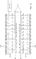
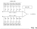
- Figure 14 shows "phase 5" of the calibration procedure, in which the residual voltage for each capacitor "n” is converted using a subset ("SUB" ADC) of the CDAC 81, made up by the five LSB capacitors, which will not themselves be calibrated (including the 0.5C weighted capacitor normally used for noise-shaping). The output of this conversion is the digitized residual voltage.
- SAB subset
- Phases 1 to 5 are repeated X number of times to get X conversions of the residual voltage, for each capacitor n, that is to be calibrated-e.g. the top six most significant capacitors C512 to C16.
- the X number of results for each individual capacitor shall be averaged in order to suppress noise for higher accuracy (similar as setting oversampling in normal operation).
- the average of X results from X conversions on the residual voltage for capacitor n is referred to as V xn .
- the output of this conversion will be referred to here as 11-bit, which is the same resolution as the ADC core in normal operation.
- the result of this conversion is adjusted, in a final digital output stage 89, so that it is centred around mid-code of the ADC 80.
- the output result of the conversions when running the calibration routine is in the six LSBs of PADC_BOUT_0V8-i.e. the underlined bit of: 12'b0000 0000 0000 .
- the last bit may be ignored in normal operation.
- the LSB of the 12-bit output is only considered in the calibration routine, but these six bits may be mapped to a 11-bit resolution, and the ADC output in normal operation will be 11-bit.
- Calibration coefficients can then be calculated for the ADC 80 as described below. These calculations may be implemented in software, executing on a microcontroller or other processor attached to the ADC 80, or could potentially be implemented in hardware.
- the capacitors will not have the perfect weights as shown in the figure, but they will have an error.
- the six MSB capacitors are calibrated, which results in six calibration coefficients, from N down to N-5.
- the calibration coefficients will either be added or subtracted from the raw output data, depending if its corresponding bit is 1 or 0 respectively by a logic stage 92 in the digital output circuitry 83.
- this 11-bit result is expanded to 16 bits, in a first digital stage 88, by multiplying by 2 5 . Then X samples of each residual voltage V xn are averaged, by performing phases 1 to 5 of the calibration switching X times, storing results from each run as a 16-bit numbers, and averaging all the results. This averaging, or decimation, filter is applied by a logic stage 93 in the digital output circuitry 83. Then these 16-bit values for V xn can be used in the equations for V eN and V en to calculate the calibration coefficients.
- PADC_BOUT_0V8 11'b100 000X XXXX
- PADC _ BOUT_ 0 V 8 _ CALIBRATED PADC _ BOUT _ 0 V 8 + Coeff 512 _ 16 b ⁇ Coeff 256 _ 16 b + Coeff 128 _ 16 b + Coeff 64 _ 16 b Coeff 32 _ 16 b + Coeff 16 _ 16 b
- the MSB bit that corresponds to Coeff 512_16b is 1, so this coefficient is added to the final result, while the rest of the bits are 0, so these are subtracted from the result.
- the X's means that there are no calibration coefficients related to these bits.
- PADC_BOUT_0V8 is expanded to 16-bit before the calibration operation takes place.
- the final resolution of the output should be at least 12 bits.
- This calibration is efficient, and with a standard deviation for the unit capacitors of 1.5%, is expected to give a mean improvement in SFDR of 15dB for the ADC 80.
- the calibration may, at least in some embodiments, be run only occasionally, e.g. on boot up after a reset.
- the ADC 80 may be set to run without calibration in normal operation, e.g. until the next device reset.
Landscapes
- Engineering & Computer Science (AREA)
- Theoretical Computer Science (AREA)
- Analogue/Digital Conversion (AREA)
Abstract
Description
- This invention relates to analog to digital conversion circuitry.
- Noise-shaping successive-approximation-register analog to digital converters (SAR-ADCs) achieve high accuracy with good power efficiency by introducing concepts from sigma-delta (ΔΣ) ADCs into SAR-ADCs. They do this by taking the residue voltage, left on the top plates of the capacitor digital-to-analog converter (CDAC) after each bit-cycling conversion, and feeding the residue into a filter which then subtracts it from the next analog sample. One structure that can be used to implement such noise-shaping is an error-feedback structure, in which the residue voltage is fed back to the input of the SAR-ADC and is subtracted from the next sample at the input.
- The residue voltage represents a combination of the different noise sources present in the ADC, such as quantization noise and comparator noise. By performing this residue subtraction operation over a series of consecutive samples, low-frequency noise can be suppressed, at the cost of increased high-frequency noise. By oversampling the input, a decimation filter can then be applied at the output of the SAR-ADC to remove the high-frequency noise, resulting in an improvement in accuracy over a similar SAR-ADC without noise-shaping.
- Adding such error-feedback can, however, add to the size and power consumption of the ADC, which is undesirable.
- Embodiments of the present invention seek to provide a more efficient design of error-feedback SAR-ADC conversion circuitry.
- From a first aspect, the invention provides analog to digital conversion circuitry, comprising:
- an input sampling buffer, comprising an input sampling capacitor, for sampling an analog signal; and
- a successive-approximation-register analog to digital converter (SAR-ADC) arranged to convert the analog signal, sampled by input sampling buffer, to a digital signal,
- From a second aspect, the invention provides an analog to digital conversion method, comprising:
- sampling an analog signal with an input sampling capacitor;
- using an amplifier and a gain-control capacitor, connected in feedback with the amplifier, to apply gain to the analog signal sampled by the input sampling capacitor;
- converting the analog signal to a digital signal using successive-approximation-register analog to digital converter (SAR-ADC); and
- decoupling the gain-control capacitor from the input sampling capacitor and feeding a residue voltage from the SAR-ADC back to the gain-control capacitor, such that the level of the analog signal, after gain is applied, is determined, at least in part, by a residue voltage previously received onto the gain-control capacitor.
- Thus it will be seen that, in accordance with embodiments of the invention, the same gain-control capacitor is used both as a feedback capacitor for the amplifier (to determine the gain applied to the sampled analog signal) and also for receiving a residue voltage from the SAR-ADC. The residue voltage can thus be conveniently used to affect the level of the subsequent sample-e.g. by being subtracted from the input signal-without having to provide a dedicated separate residue buffer, comprising one or more additional capacitors, in addition to the capacitors in the input sampling buffer, and without requiring a second amplifier for transferring the residue voltage. Embodiments can therefore be particularly efficient both in area and power consumption.
- Moreover, using the same gain-control capacitor both for passing samples into the SAR-ADC and for receiving a residue voltage back from the SAR-ADC, avoids any need to transfer the voltage residue between buffers, ensuring no attenuation losses and avoiding a requirement for dynamic amplification, which might otherwise require complex calibration to mitigate process, temperature and voltage variations.
- The analog to digital conversion circuitry is preferably arranged to provide error-feedback noise-shaping. It may be configured to oversample the input signal. It may comprise a decimation filter for down-sampling the digital signal generated by the SAR-ADC. The use of noise-shaping in preferred embodiments can advantageously provide increased accuracy, albeit with lower effective bandwidth, without having to increase the area, and therefore the power consumption, e.g. when the ADC is implemented as an integrated circuit.
- The gain, determined by the gain-control capacitor, may be positive or it may be negative (i.e. to attenuate the analog signal, if the supply input range is too large for the SAR-ADC). The gain-control capacitor may be of fixed or variable capacitance. The gain may be configurable.
- The analog to digital conversion circuitry may comprise a control interface for receiving control signals, e.g. from a processor or microcontroller.
- The successive-approximation-register analog to digital converter may be a differential converter. It may comprise respective positive and negative paths. The amplifier may be a differential amplifier. The input sampling buffer may comprise a pair of input sampling capacitors, which may be of the same nominal capacitance. It may comprise a pair of gain-control capacitors, which may be of the same nominal capacitance. These capacitor pairs may be provided on respective positive and negative paths of the differential converter.
- The amplifier may be an operational transconductance amplifier (OTA).
- The input sampling buffer preferably comprises a set of one or more switches for switching between the amplification configuration (i.e. state, or mode of operation) and the error-feedback configuration (i.e. state, or mode of operation). It may comprise a plurality switches for selection of the amplification and error-feedback configurations. A first subset of the switches may be closed when operating in the amplification configuration and open when not in the amplification configuration. A second subset of the switches may be closed when operating in the error-feedback configuration and open when not in the error-feedback configuration. The input sampling buffer may thus be switched between the configurations (and any optional further configurations) by selectively opening and closing switches.
- The ADC circuitry may comprise control logic for controlling the switches. The control logic may comprise a hardware finite state machine. The control logic may be implemented in hardware (e.g. using dedicated sequential logic), or it may be implemented in software, or by a combination of hardware and software. When using software, the ADC circuitry may comprise a processor and a memory storing software for execution by the processor.
- The input sampling buffer may be configured to receive the analog signal onto the input sampling capacitor when in the error-feedback configuration. However, in other embodiments, the input sampling buffer may have a sampling configuration, in which it is configured to receive the analog signal onto the input sampling capacitor, which may be distinct from the error-feedback configuration and/or from the amplification configuration.
- The ADC circuitry may control the input sampling buffer to cycle between the error-feedback configuration and the amplification configuration (optionally also passing through one or more further configurations) at a sampling rate. It may cycle once for each sample of a succession of samples provided to the SAR-ADC from the input sampling buffer.
- The residue voltage from one sample may influence the level of a subsequent-e.g. the next-sample provided to the SAR-ADC. The input sampling buffer may be arranged to subtract the residue voltage from the next sample-i.e. to provide the SAR-ADC with the difference between the residue voltage and the sample with nominal gain applied.
- The gain-control capacitor may be arranged to be connected in parallel with the amplifier when the input sampling buffer is in the amplification configuration.
- The input sampling buffer may comprise one or more dedicated-error-feedback capacitors, each arranged to be switchably connected in feedback with the amplifier (i.e. arranged to be switchably connected in parallel with the amplifier). Each dedicated-error-feedback capacitor may be switchable independently from the gain-control capacitor. This may, in some embodiments, allow the gain-control capacitor and one or more dedicated-error-feedback capacitors to be connected in feedback with the amplifier, when in the error-feedback configuration. This can allow the gain to be adjusted for different situations. The gain-control capacitor and the one or more dedicated-error-feedback capacitors may be connected in parallel with each other when in the error-feedback configuration. Switches may allow the dedicated-error-feedback capacitors to be decoupled (i.e. not used) when in the amplification configuration. In this way, the feedback capacitance applied to the amplifier can be different in the two configurations. This may be useful e.g. for setting coefficients in the filter transfer function, when using a higher-order filter, through selectively attenuating the error-feedback voltage.
- The SAR-ADC preferably comprises a capacitor digital-to-analog converter (CDAC), which may be a differential CDAC. The ADC circuitry preferably comprises control logic for performing bit-cycling with CDAC. The residue voltage may be received from the top plates of the capacitors of the CDAC. A positive residue voltage component may be received from a positive side of the CDAC by a positive-side gain-control capacitor, in the error-feedback configuration, and a negative residue voltage component may be received from a negative side of the CDAC by a negative-side gain-control capacitor.
- The ADC circuitry may, in some embodiments, comprise calibration circuitry for performing a calibration of the SAR-ADC. It may be configured to calibrate each of a set of a capacitors of a CDAC of the SAR-ADC. It may calibrate a strict subset of the capacitors, which may be a succession of the most significant capacitors of the CDAC-i.e. a subset of capacitors of CDAC each having larger capacitance than any of the capacitors of the CDAC that are not in the subset. The calibration circuitry may be arranged to calibrate one capacitor or one differential capacitor pair at a time. It may calibrate the capacitors in order from largest to smallest.
- Such calibration may improve the linearity of the SAR-ADC. In some embodiments, it may be advantageously implemented by digital control, without requiring any additional analog circuitry. The calibration circuitry may be arranged, when calibrating a capacitor (or capacitor pair), to switch capacitors of the CDAC so as to generate a residual voltage that is proportional to a mismatch between the capacitor being calibrated and one or more further capacitors of the CDAC. It may determine a mismatch between the capacitor under calibration and a set of other capacitors of total nominal capacitance equal to the capacitor under calibration.
- The ADC circuitry may support a calibration configuration (i.e. a calibration state or mode), in which the gain-control capacitor is decoupled from the input sampling capacitor and is arranged to receive a mismatch voltage from the SAR-ADC. In this way, an error-feedback noise-shaping loop may be used to sample a residual mismatch voltage, which resides on the top plates of the CDAC after the switching. This efficient use of the input sampling buffer also for calibration can avoid the need for additional analog components and capacitors to provide calibration. Sampling the mismatch residue onto the gain-control (error-feedback) capacitor can also advantageously allow the SAR-ADC to be reset without the mismatch residue being deleted by the reset. The calibration circuitry may be arranged to convert the mismatch voltage with the SAR-ADC. It preferably does so using a succession of the least significant capacitors of a CDAC-i.e. using a mismatch-sampling subset of capacitors of the CDAC, each having capacitance no larger than any of the capacitors of the CDAC that are not in the mismatch-sampling subset.
- Use of this mismatch-sampling subset of the SAR-ADC, together with oversampling, can give a highly accurate measurement of the error residual voltage due to mismatch, in a compact implementation. For each capacitor being calibrated, a plurality of samples may be taken and averaged to suppress noise and increase accuracy. The ADC circuitry may be configured to calculate calibration coefficients from digital measurements, output by the SAR-ADC, of the mismatches of a set of capacitors of the SAR-ADC. These coefficients may be used to increase linearity of the ADC in subsequent operation. The ADC circuitry may be configured to adjust the digital signal output by the SAR-ADC in dependence on one or more of the calibration coefficients-e.g. being configured to add or subtract one or more calibration coefficients from subsequent digital samples.
- In any of the embodiments disclosed herein, the ADC conversion circuitry may be provided by an integrated-circuit device, such as a system-on-chip. It may be integrated as a peripheral to a processor, such as microcontroller. It have an input for receiving the analog signal and/or an output for outputting the digital signal.
- Features of any aspect or embodiment described herein may, wherever appropriate, be applied to any other aspect or embodiment described herein. Where reference is made to different embodiments or sets of embodiments, it should be understood that these are not necessarily distinct but may overlap.
- Certain preferred embodiments of the invention will now be described, by way of example only, with reference to the accompanying drawings, in which:
-
Figure 1 is a schematic architectural diagram of an ADC, embodying the invention, having a programmable-gain switched-capacitor input sampling buffer and an SAR-ADC for converting the samples from the sampling buffer; -
Figure 2 is a close-up view of part ofFigure 1 ; -
Figure 3 is a simplified schematic diagram showing the input sampling buffer in an error-feedback configuration; -
Figure 4 is a simplified schematic diagram showing the input sampling buffer an amplification configuration; -
Figure 5 is a more-detailed diagram of the input sampling buffer; -
Figure 6 is a timing diagram of the ADC and buffer operation when error-feedback noise-shaping is enabled; -
Figure 7 is a timing diagram of the ADC and buffer operation when error-feedback noise-shaping is disabled; -
Figures 8A &8B are split parts of a simplified schematic architectural diagram of another ADC, embodying the invention, that is self-calibrating; and -
Figures 9 ,10 ,11 ,12 ,13 &14 are schematic diagrams of parts of the self-calibrating ADC ofFigure 8 , in different respective states, during successive steps of a calibration procedure. -
Figure 1 shows the high-level architecture of an analog-to-digital converter (ADC) 1 circuit portion. It may, in some embodiments, be incorporated as a peripheral within an integrated-circuit system-on-chip (SoC), such as a digital radio on a chip, or it may be used in any other appropriate context. The initials "PADC" are used in the drawings as an abbreviation for "peripheral ADC", in contemplation of theADC 1 being a peripheral of a microcontroller unit, but this is only by way of example. - The
ADC 1 has a programmable-gain switched-capacitorinput sampling buffer 2, which is coupled to an SAR-ADC 3 for converting the samples sampled by thebuffer 2. - Through the innovative use of feedback, as explained below, this
ADC 1 enables first-order error-feedback noise-shaping, where theinput sampling buffer 2 is reused as a loop filter. This configuration gives a signal transfer function STF=1, and a noise transfer function NTF=1-z-1. - The SAR-
ADC 3 comprises a differential capacitor digital-to-analog converter (CDAC)array 4 which feeds into acomparator 5. It also has a control block control logic,SAR_CTRL 6, andoutput circuitry 11. - The
input sampling buffer 2 has positive and negative paths that can be coupled to an operational transconductance amplifier (OTA) 8 and capacitors C1, C1', C2, C2', through a set of switches, the operation of which is described below. The switches are shown in simplified schematic form inFigure 2 , represented by six switches on each of the positive and negative sides, but a more detailed implementation using twenty-eight switches, labelled S1-S14, S1'-S14', is also shown inFigure 5 . The switches are controlled by the control block control logic,SAR_CTRL 6 or by a higher-level state machine. - Features of the
input sampling buffer 2 and SAR-ADC 3 that particularly support the noise-shaping operation are shown in four dashedrectangles - To perform noise-shaping, the control logic,
SAR_CTRL 6, controls the SAR-ADC 3 to convert a sample, sampled by theinput buffer 2, in a conventional manner, by performing SAR bit-cycling with tencapacitors 7, "C512", "C256", ..., "C4", "C2", "C1", of theCDAC 4. Here, "C" represents one unit capacitance, so "C512" indicates 512 unit capacitors. - The
SAR_CTRL 6 then switches a respective pair offurther capacitors 10, "C0.5", on each of the positive and negative sides, after the conversion, to get the residual voltage, by dividing the voltage after the least-significant-bit (LSB) decision in two. Each of the C0.5capacitors 10 equals the C1 capacitors split in two; they do not suffer the same mismatch requirement as the rest of theCDAC 4. - Considering the positive side, after switching the C0.5 capacitor, the
SAR_CTRL 6 enables two feedback switches 9 (ϕErrorFB) to switch theinput sampling buffer 2 to an error-feedback configuration. Theinput sampling buffer 2 then transfers the residue voltage from the top plates of theCDAC 4 to a gain-control feedback capacitor C2 in theinput sampling buffer 2, and to corresponding capacitor C2' on the negative side. (Note, these are different from the capacitors "C2" in theCDAC 4.) -
Figure 2 shows a close-up of theinput sampling buffer 2. At the same time as conversion and error-feedback are performed, the next sample can be collected on the input sampling capacitors C1 and C1'. (Note, these are different from the capacitors "C1" in theCDAC 4.) -
Figure 3 provides a simplified schematic view of theinput sampling buffer 2 still in the error-feedback configuration, showing the effect of the switches but omitting the switches themselves, to highlight how the next sample can be collected on C1 and C1', which are decoupled from theCDAC 4. When the transfer of residue voltage from theCDAC 4 to the feedback capacitor C2 in finished, and the sampling on C1 is also finished, theSAR_CTRL 6 operates the switches in theinput sampling buffer 2 to set thebuffer 2 to an amplification configuration, as shown inFigure 4 . -
Figure 4 provides a simplified schematic view of theinput sampling buffer 2 in the amplification configuration (again showing the effect of the switches, but not the switches themselves). In this configuration, the next sample is transferred from the capacitors C1, C1' onto theCDAC 4, through theOTA 8. However, the gain-control feedback capacitors C2, C2' are also coupled between the inputs and outputs of theOTA 8 so as to remove the voltage residue stored on the capacitors C2, C2', obtained from the previous sample, thereby transferring the difference between the sampled input voltage and the residue voltage to theCDAC 4. In this way error-feedback is applied to the new sample, as can be seen in the values of the voltages as shown inFigures 3 &4 . - To obtain one sample with noise-shaping, the
ADC 1 can be controlled to take a number, X, of samples, by performing the operations above to obtain each of these X samples. The result from each of the X samples is passed to a digital decimation filter, in theoutput circuitry 11, to filter out of band noise. The output of the decimation filter is one sample out per X samples in. This provides noise-shaping through oversampling and decimation. -
Figure 5 is more-detailed schematic diagram of theinput sampling buffer 2. - It shows how the capacitance C2, on each path, may be implemented as two separate capacitors: a gain-control feedback capacitor C2a, which is used both for determining the gain applied to samples and as an error-feedback capacitor for capturing the residue voltage from the SADC, and a dedicated error-feedback capacitor C2b, which is used for capturing the residue in parallel with C2a. The capacitors C2a and C2b are of equal size. The provision of C2b in addition to C2a allows the gain to be adjusted. When transferring the residue voltage, both C2a and C2b are connected. When capturing the feedback, the capacitor C2b is either kept connected, together with C2a, or is disconnected, depending on a configurable gain setting. The total size of C2 is designed to match the total size of the
CDAC 4, so as to get a gain of one in the transfer of the residue voltage. In some embodiments, one or more further dedicated error-feedback capacitors, C2c, C2d, C2e, etc., may be provided similarly, and can be switchably coupled in parallel with C2a to provide further gain control. - When configured for amplification, the role of the
input sampling buffer 2 is to take the I/O supply input range and divide it down to a reasonable range for the SAR-ADC core 3. In one example embodiment, it has a configurable range of gain settings, from 2/3 (e.g. 1.8Vppd with a 1.2V reference) to 4 (e.g. 300mVppd with a 1.2V reference). - The following phases for the switches are labelled in
Figure 5 , and their activations are shown in more detail in the timing diagrams inFigures 6 and7 : - ϕ1 : phase for sampling; ϕ1a indicates this is switched in advance to 1.
- ϕ2: input amplification phase; input sample is transferred to the
CDAC 4. The amplification gain is C1/C2, where C2 depends on the gain configuration. C2 may equal C2a, or it may equal C2a + C2b (if S11 & S14 are also activated, as explained below), or more generally C2 may equal C2a+C2b+C2c+C2d+... when further switchable capacitors are connected. - ϕ3: error-feedback phase; error residue is transferred from the
CDAC 4 to C2b (and also to C2a through ϕ4). This residue will remain on C2 for the next ϕ2 to subtract it from input sample. - ϕ4: this phase is a combination of ϕ2∥ ϕ3 . If operating with noise-shaping disabled, then ϕ4=ϕ2, but with noise-shaping enabled, it will be enabled by ϕ3 in order to capture the residue, and is kept high until is ϕ2 done.
- ϕ5: RESET and AZ (autozero) phase; for autozeroes and resets the OTA feedback capacitors. Non-overlapping with ϕ2, ϕ3 and ϕ4 and enabled when entering Idle or Convert states, described below. (The
OTA 8 itself is autozeroed in the reset phase to cancel any offset voltage in theOTA 8.) - For some gain settings, the switches S11 and S14 may also be enabled in phase ϕ2 (i.e. in the input amplification phase) so that the feedback capacitor C2b is also connected, in parallel with the gain-control capacitor C2a, in the amplification configuration, in order to provide a desired gain for the
ADC 1. The amplification gain during the amplification phase will then C1/(C2a+C2b). Where further capacitors C2c, C2d, etc. are provided, further switches can be operated to provide finer gain control. - The error-feedback noise-shaping can be turned on and off through the control logic 6 (e.g. by a microcontroller).
-
Figure 6 is a timing diagram for the buffering and conversion operations when error-feedback noise-shaping is enabled. -
Figure 7 is a timing diagram for the buffering and conversion operations when error-feedback noise-shaping is disabled. - They show the following signals and states:
- PWRUP_PADC: a control-input signal to power-up the
ADC 1; - PADC_NOISEHAPING: a control-input signal to enable (or disable) error-feedback noise-shaping;
- PADC_SAMPLE: a control-input signal to initiate capture of a sample;
- PADC_CONVERT: control input to initiate conversion of the captured sample;
- PADC_MAIN_FSM: represents the different states of a main finite state machine (FSM) within the control logic SAR_CTRL 6: OFF, Idle, Sample, Amplify, Convert, Sample&Convert, Done. The Sample state is entered only for the first sample after power up, with Sample&Convert being used for all subsequent samples. Sample&Convert allows for "pipelined" sampling, in which the next sample is collected while the previous sample is converted, so whenever Sample goes high while in Convert, the Sample&Convert state is entered;
- PADC_BITCYCLE_FSM: represents the different states of a bit-cycling finite state machine (FSM) within the control logic SAR_CTRL 6: OFF, BitCycling, Error feedback, Done, RESET.
- The following four signals are output from the
control logic SAR_CTRL 6 or from a higher-level state machine, and are distributed to the blocks that need them as appropriate: - INT_SAMPLE: an internal signal for sampling;
- INT_AMPLIFY: an internal signal for amplifying the input;
- INT_CONVERT: an internal signal for converting the sample;
- INT_DONE: an internal signal indicating conversion is done;
- As can be seen from the timing diagrams, the main FSM cycles through the same states whether or not noise-shaping is enabled. However, when noise-shaping is disabled, as in
Figure 7 , the switch phase ϕ3 is never activated. When noise-shaping is enabled, as inFigure 6 , the bit-cycling FSM enters an Error feedback state, after the BitCycling state, which causes the switch phase ϕ3 to be active, as shown, causing theinput sampling buffer 2 to enter the error-feedback configuration, described above. The switch phase ϕ4 is also different when noise-shaping is enabled, to capture the residue on the capacitors C2a and C2b when the feedback path is connected. The timing diagrams show the signal flow when the gain of the input amplification is one, i.e. C2a=C1 in size in this scenario, with C2b being disconnected before the amplification phase is entered. -
Figure 8 (split acrossFigures 8a &8b ) shows another SAR-ADC 80, embodying the invention, that again provides error-feedback noise-shaping, but with additional features for performing linearity calibration. - This
ADC 80 has been designed with acustom CDAC 81 where the focus has been to reduce the amount of capacitance to a minimum to save power. The down side of this is higher mismatch and more noise. However, the error-feedback noise-shaping helps to mitigate the noise penalty. Noise-shaping may be used to reach very high accuracies on low frequencies. Linearity calibration is provided to achieve good linearity even in high accuracy modes. Linearity calibration enables the linearity to get to the same levels as noise where SNR (signal-to-noise ratio) ≤ SFDR (spurious free dynamic range). -
Figure 8 shows a high-level architectural diagram of parts of the analog and digital portions of theADC SAR core 80. TheADC 80 has an input sampling buffer (not shown inFigure 8 , although represented schematically inFigure 12 &13 ), similar to theinput sampling buffer 2 ofFigure 1 above. This is connected to a differential CDAC 81 (only the positive side is shown inFigure 8 for simplicity, but there is also a similar negative side), and controllogic SAR_CTRL 82, similar to theSAR_CTRL 6 described above. - The
ADC 80 also has higher-level digitallogic output circuitry 83, comprising a calibration controllogic block DIG_CAL_CTRL 87, for initiating and controlling the calibration procedure, by outputting appropriate control signals to theADC 80, and for processing 12-bit digital output words received from a set of twelveflip flops 84 at the output of acomparator 85 of theCDAC 81. Thiscircuitry 83 enables the capacitors to be measured in turn, and stores the results for further calculations. Thisdigital control circuitry 83 may be implemented in hardware, as state machine implemented with dedicated logic gates, or it may be implemented at least partly by software executing on a processor of the device. - Notable features involved in the linearity calibration are indicated by dashed
boxes - A lower-level calibration control
logic block CAL_CTRL 86 handles internal operations of theADC 80 by controlling switching during the calibration switching procedure, under the higher-level control of the calibration controllogic block DIG_CAL_CTRL 87. These twoblocks features 91 involved in the linearity calibration. This particularexemplary ADC 80 is intended as an 11-bit ADC, so theCDAC 81 has tenmain capacitors 81a, labelled "C1" up to "C512", on each side, where C is one unit capacitance, and where 512C means 512 unit capacitors. C1 to C512 therefore form a 10-bit CDAC. The reason this 11-bit ADC needs only a 10-bit CDAC 81 is that it implements a VCM-based (common-mode-voltage based) switching scheme, which removes the need for the most-significant-bit (MSB) capacitor that, in a conventional 11-bit SAR-ADC, would be weighted 1024C. - The
first capacitor 81b of a pair of 0.5C capacitors "C0.5", on the positive side, is provided to achieve noise-shaping as described above with reference toFigure 1 . Thiscapacitor 81b is only switched when noise-shaping is activated to get the correct residue voltage to feed into the noise-shaping loop filter. The second 0.5C capacitor 90 is used in the linearity calibration scheme, so that in an ideal case, the MSB capacitor "C512" of themain bank 81a, divided by the capacitances of the other ninemain capacitors 81a, plus the two half-LSB capacitors 8b & 90, equal 512C/(256C+128C+..0.5C+0.5C) =1. - The calibration procedure uses a switching scheme to provoke, and then convert, a residual voltage due to capacitor mismatch, and then implements an algorithm to use this converted residual to calculate calibration coefficients.
-
Figures 9-14 illustrate the calibration procedure by showing states of the analog side of theADC 80 during five main phases the procedure. Thesephases 1 to 5 are repeated X number of times to get X conversions of the residual voltage, for each capacitor that is to be calibrated. In this embodiment, the top six most-significant capacitors, C512 to C16, are calibrated, while the five least-significant capacitors, C8, C4, C2, C1, C0.5, are used to convert any mismatch voltage, as explained below. Since the largest capacitors contribute most to the linearity of theADC 80, it may be sufficient to leave the smallest capacitors uncalibrated. -
Figure 9 shows "phase 1" of the calibration procedure, in which the inputs of theADC 80 are shorted and a regular sample is taken with theADC 80. The voltage VBUF_CM is the output common mode from the OTA, PADC_BUF 120 (seeFigures 12 &13 ), of the input sampling buffer of theADC 80. When taking a sample with the inputs of theADC 80 shorted, the inputs of the input sampling buffer are shorted, so that both positive (P) and negative (N) sides of theADC 80 will be charged to the buffer output common mode, and the differential voltage, VDIFF, is 0V. Afterphase 1, the sample taken in that phase is not converted normally, but instead the bottom plates in theCDAC 81 are switched according toFigure 10 . Although not shown inFigures 9 and10 , theADC 80 has an input sampling switch that is closed while sampling the VBUF_CM (VDIFF=0), and that is opened to perform the switching operation shown inFigure 10 - The capacitors are calibrated individually in "
phase 2" of the calibration procedure, starting the from the largest, most significant bit (MSB) capacitors and working downwards. -
Figure 10 shows an example in which theMSB cap 100 is being calibrated, which should ideally be weighted 512C, where C = 1 unit capacitance. In this "phase 2", on the positive side, thecapacitor 100 to be calibrated is switched to VREF and the rest of the bottom plates are switched to GND. On the negative side, the corresponding capacitor 100' is switched to GND with the rest of the bottom plates being set to VREF. In an ideal case, this would give a division that should result in 1 as explained above, but due to mismatch the result will not be exactly 1, and there will be a differential voltage between the P and N side that corresponds to the mismatch between C512 and the rest of the capacitors. On the P-side, this gives "V_RES_P", and on N-side it gives "V_RES_N". -
Figure 11 illustrates measuring the MSB-2 capacitor C128, weighted 128C. The two capacitors (MSB, C512 and MSB-1, C256) that have already been measured and converted (i.e. for which phases 1 to 5 have been completed) are kept at VCM, while the rest are switched in order to get the division C128/(C64+C32..+C0.5+C0.5). This switching procedure provokes the mismatch residue voltage on the top plates of theCDAC 81. This residual voltage is sampled into the noise-shaping loop, using the input sampling buffer. The residual voltage is similar in magnitude from the residual voltage that is used in the noise-shaping mode. -
Figure 12 shows "phase 3" of the calibration procedure, which uses the error feedback from the noise-shaping procedure to sample the residual voltage generated fromphases 1 & 2 on the feedback capacitors in the buffer. The input-sampling capacitor pair, C_SAMP_P & C_SAMP_N (equivalent to C1 & C1' in the embodiment ofFigure 2 ) are here disconnected from the gain-control feedback capacitors, C_FB_P & C_FB_N (equivalent to C2 & C2' in the embodiment ofFigure 2 ). In particular, the residual voltage generated by the switching inphase 2 that is left on the top plates of theCDAC 81 is sampled by the error feedback noise-shaping loop, similar to the residual voltage during error feedback noise-shaping. In this way, the error feedback noise-shaping loop functions as a second input to theADC 80, and the SAR logic can be reset after the residue is sampled, so that it will be ready for conversion by a "sub" ADC, formed of a capacitor subset consisting of the five least significant bit (LSB) capacitors, C8, C4, C2, C1, C0.5, which will not be calibrated. One important element in this step is the matching between the feedback capacitor pair, C_FB_P & C_FB_N, and theCDAC 81. If the ratio CDAC/CFB is not 1, there will be a "gain error" in the charge transfer of V_RES. It is expected that a tolerance of +/-20% gain error will be acceptable in the present design. - Sampling the mismatch residue onto the error-feedback capacitor C_FB (C2) allows the SAR-
ADC 80 to be reset without the mismatch residue being deleted by the reset. Resetting allows the bottom plates and SAR logic to be reset back to the state it was in before the switching to provoke the mismatch voltage was performed, i.e. in its "IDLE" state, where all bottom plates are switched to VCM and the SAR logic is ready for bit cycling. -
Figure 13 shows "phase 4" of the calibration procedure, in which the sampled residual voltage fromphase 2 is transferred back onto theCDAC 81 top plates of the SAR-ADC 80, while the inputs of theADC 80 are shorted, as the SAR-ADC 80 is now reset and ready for conversion. The residue voltage was sampled on the feedback capacitors in the previous phase, while input capacitors of PADC_BUF were shorted, so that V_RES_P - V_RES_N is the only differential voltage being transferred back to theCDAC 81. -
Figure 14 shows "phase 5" of the calibration procedure, in which the residual voltage for each capacitor "n" is converted using a subset ("SUB" ADC) of theCDAC 81, made up by the five LSB capacitors, which will not themselves be calibrated (including the 0.5C weighted capacitor normally used for noise-shaping). The output of this conversion is the digitized residual voltage. -
Phases 1 to 5 are repeated X number of times to get X conversions of the residual voltage, for each capacitor n, that is to be calibrated-e.g. the top six most significant capacitors C512 to C16. The X number of results for each individual capacitor shall be averaged in order to suppress noise for higher accuracy (similar as setting oversampling in normal operation). The average of X results from X conversions on the residual voltage for capacitor n is referred to as Vxn. - Even though the conversion of the residual "mismatch" voltage essentially uses a "6 bit" ADC, the output of this conversion will be referred to here as 11-bit, which is the same resolution as the ADC core in normal operation. The result of this conversion is adjusted, in a final
digital output stage 89, so that it is centred around mid-code of theADC 80. The ADC output is encoded as offset binary, and mid-code is when PADC_IP-PADC_IN = 0, which gives PADC_BOUT_0V8 = 11'b100 0000 0000. This output may be extended with 1 bit, to be 12 bit, in some situations, and mid code will then be PADC_BOUT_0V8 = 12'b1000 0000 0000. So, the output result of the conversions when running the calibration routine, is in the six LSBs of PADC_BOUT_0V8-i.e. the underlined bit of: 12'b0000 0000 0000. In some embodiments, the last bit may be ignored in normal operation. Thus, the LSB of the 12-bit output is only considered in the calibration routine, but these six bits may be mapped to a 11-bit resolution, and the ADC output in normal operation will be 11-bit. The 6-bit output, when encoded as offset binary, can vary from -32 to +31, where 6'b00 0000 = -32 and 6'b11 1111 is +31. These values may be mapped to the equivalent values in 11-bit resolution, meaning -32 to +31 where 11'b011 1110 0000 is -32 and 11'b100 0001 1111 is +31. - Calibration coefficients can then be calculated for the
ADC 80 as described below. These calculations may be implemented in software, executing on a microcontroller or other processor attached to theADC 80, or could potentially be implemented in hardware. - Because of non-linearities, the capacitors will not have the perfect weights as shown in the figure, but they will have an error. The actual capacitor value that includes this error can be written as

CDAC 81, and N is the number of the MSB capacitor. TheCDAC 81 in thisexemplary ADC 80 is 10bits, and the two 0.5C weighted capacitors can be numbered 1 and 1 (or 1A and 1B, to distinguish them). This deviation from ideal weights will manifest itself as an error voltage for each capacitor switch operation performed, and this error voltage can be expressed as
- The total linearity error can be expressed as

- After the switching operations are done for a capacitor n in
phase 1 andphase 2, there will be a residual voltage left on the top plates of theCDAC 81 that can be used to calculate the individual error voltage for the respective capacitor n. In adifferential ADC 80, the calibration coefficient, or error voltage, of the MSB capacitor can be expressed as
- So, once the residual voltage VxN is converted, it need only be divided by 4 to get the error voltage, or calibration coefficient, related to the MSB capacitor. The rest of the calibration coefficients can be found by evaluating the equation

- In the
ADC 80, the six MSB capacitors are calibrated, which results in six calibration coefficients, from N down to N-5. When calibrating the ADC output during normal operation, the calibration coefficients will either be added or subtracted from the raw output data, depending if its corresponding bit is 1 or 0 respectively by alogic stage 92 in thedigital output circuitry 83. - When running the conversions on residual voltages from the calibration switching procedure, the six bits with the results from the conversion are mapped to offset-binary-encoded 11-bit resolution, meaning the result will be in the range -32 to +31 where 11'b011 1110 0000 is -32 and 11'b100 0001 1111 is +31. This is done by just adding the 6-bit result 6'bXXXXXX to 11'b011 1110 0000. This makes sure that when the mid code for the 6-bit results = 6'b10 0000 is added to 11'b011 1110 0000, it gives 6'b10 0000 + 11'b011 1110 0000 = 11'b100 0000 0000 = 0, which is mid code.
- To calculate the calibration coefficients, this 11-bit result is expanded to 16 bits, in a first
digital stage 88, by multiplying by 25. Then X samples of each residual voltage Vxn are averaged, by performingphases 1 to 5 of the calibration switching X times, storing results from each run as a 16-bit numbers, and averaging all the results. This averaging, or decimation, filter is applied by alogic stage 93 in thedigital output circuitry 83. Then these 16-bit values for Vxn can be used in the equations for VeN and Ven to calculate the calibration coefficients. - This will result in six calibration coefficients [Coeff512_16b Coeff256_16b Coeff128_16b Coeff64_16b Coeff32_16b Coeff16_16b], which will be added or subtracted from the PADC_BOUT_0V8 value depending on the corresponding bit decision. This means that, for the result PADC_BOUT_0V8 =11'b100 000X XXXX, the final calibrated result will be

- The MSB bit that corresponds to Coeff512_16b is 1, so this coefficient is added to the final result, while the rest of the bits are 0, so these are subtracted from the result. The X's means that there are no calibration coefficients related to these bits.
- The result PADC_BOUT_0V8 =11'b011 111X XXXX, would give

- Since the calibration coefficients are 16 bits, PADC_BOUT_0V8 is expanded to 16-bit before the calibration operation takes place. In order to benefit from the calibration, the final resolution of the output should be at least 12 bits.
- This calibration is efficient, and with a standard deviation for the unit capacitors of 1.5%, is expected to give a mean improvement in SFDR of 15dB for the
ADC 80. - Typically, the mismatch of the capacitors is unlikely to change much over time, so the calibration may, at least in some embodiments, be run only occasionally, e.g. on boot up after a reset. Once the calibration coefficients are calculated, the
ADC 80 may be set to run without calibration in normal operation, e.g. until the next device reset. - It will be appreciated by those skilled in the art that the invention has been illustrated by describing one or more specific embodiments thereof, but is not limited to these embodiments; many variations and modifications are possible, within the scope of the accompanying claims.
wherein the input sampling buffer has an amplification configuration and an error-feedback configuration, wherein, when the input sampling buffer is in the amplification configuration, the input sampling capacitor is coupled to the amplifier and gain-control capacitor, with the gain-control capacitor connected in feedback with the amplifier, for applying gain to the analog signal sampled by the input sampling capacitor, and, when the input sampling buffer is in the error-feedback configuration, the gain-control capacitor is decoupled from the input sampling capacitor and is arranged to receive a residue voltage from the SAR-ADC, such that the level of the analog signal determined in the amplification configuration varies, at least in part, in dependence on the residue voltage received onto the gain-control capacitor in the error-feedback configuration.
Claims (15)
- Analog to digital conversion circuitry, comprising:an input sampling buffer, comprising an input sampling capacitor, for sampling an analog signal; anda successive-approximation-register analog to digital converter (SAR-ADC) arranged to convert the analog signal, sampled by input sampling buffer, to a digital signal,wherein the input sampling buffer further comprises an amplifier and a gain-control capacitor; andwherein the input sampling buffer has an amplification configuration and an error-feedback configuration, wherein, when the input sampling buffer is in the amplification configuration, the input sampling capacitor is coupled to the amplifier and gain-control capacitor, with the gain-control capacitor connected in feedback with the amplifier, for applying gain to the analog signal sampled by the input sampling capacitor, and, when the input sampling buffer is in the error-feedback configuration, the gain-control capacitor is decoupled from the input sampling capacitor and is arranged to receive a residue voltage from the SAR-ADC, such that the level of the analog signal determined in the amplification configuration varies, at least in part, in dependence on the residue voltage received onto the gain-control capacitor in the error-feedback configuration.
- The analog to digital conversion circuitry of claim 1, wherein the analog to digital conversion circuitry is arranged to provide error-feedback noise-shaping.
- The analog to digital conversion circuitry of claim 1 or 2, wherein the analog to digital conversion circuitry is configured to oversample the input signal and comprises a decimation filter for down-sampling the digital signal generated by the SAR-ADC.
- The analog to digital conversion circuitry of any preceding claim, wherein:the SAR-ADC is a differential converter;the amplifier is a differential amplifier; andthe input sampling buffer comprises a pair of input sampling capacitors and a pair of gain-control capacitors.
- The analog to digital conversion circuitry of any preceding claim, wherein the input sampling buffer comprises a set of one or more switches for switching the input sampling buffer between the amplification configuration and the error-feedback configuration, and wherein analog to digital conversion circuitry comprises control logic for controlling the switches.
- The analog to digital conversion circuitry of any preceding claim, wherein the input sampling buffer is configured to receive the analog signal onto the input sampling capacitor when in the error-feedback configuration.
- The analog to digital conversion circuitry of any preceding claim, wherein the analog to digital conversion circuitry is configured to control the input sampling buffer to cycle between the error-feedback configuration and the amplification configuration once for each sample of a succession of samples provided to the SAR-ADC from the input sampling buffer.
- The analog to digital conversion circuitry of any preceding claim, wherein the input sampling buffer is arranged to subtract a residue voltage determined for one sample from the next sample in a succession of samples.
- The analog to digital conversion circuitry of any preceding claim, wherein the input sampling buffer comprises one or more dedicated-error-feedback capacitors, each arranged to be switchably connected in feedback with the amplifier, independently from the gain-control capacitor.
- The analog to digital conversion circuitry of any preceding claim, wherein the SAR-ADC comprises a capacitor digital-to-analog converter (CDAC), and wherein the analog to digital conversion circuitry comprises calibration circuitry for calibrating each capacitor, or each differential capacitor pair, of a plurality of capacitors or capacitor pairs of the CDAC, wherein the calibration circuitry is arranged, when calibrating a capacitor or capacitor pair, to switch capacitors of the CDAC so as to generate a residual mismatch voltage that is proportional to a mismatch between the capacitor or capacitor pair being calibrated and one or more further capacitors or capacitor pairs of the CDAC.
- The analog to digital conversion circuitry of any preceding claim, wherein the analog to digital conversion circuitry supports a calibration configuration, for calibrating the SAR-ADC, in which the gain-control capacitor is decoupled from the input sampling capacitor and is arranged to receive a mismatch voltage from the SAR-ADC.
- The analog to digital conversion circuitry of claim 11, comprising calibration circuitry configured to use a subset of capacitors of a capacitor digital-to-analog converter (CDAC) of the SAR-ADC to convert the mismatch voltage.
- The analog to digital conversion circuitry of any preceding claim, wherein the analog to digital conversion circuitry is configured to calculate calibration coefficients from digital measurements, output by the SAR-ADC, of mismatches of a set of capacitors of the SAR-ADC, and to adjust the digital signal output by the SAR-ADC in dependence on the calculated calibration coefficients.
- An integrated-circuit device comprising the analog to digital conversion circuitry of any preceding claim.
- An analog to digital conversion method, comprising:sampling an analog signal with an input sampling capacitor;using an amplifier and a gain-control capacitor, connected in feedback with the amplifier, to apply gain to the analog signal sampled by the input sampling capacitor;converting the analog signal to a digital signal using a successive-approximation-register analog to digital converter (SAR-ADC); anddecoupling the gain-control capacitor from the input sampling capacitor and feeding a residue voltage from the analog to digital converter back to the gain-control capacitor, such that the level of the analog signal, after gain is applied, is determined, at least in part, by a residue voltage previously received onto the gain-control capacitor.
Applications Claiming Priority (1)
| Application Number | Priority Date | Filing Date | Title |
|---|---|---|---|
| GB2108885.1A GB2605466A (en) | 2021-06-21 | 2021-06-21 | Error-feedback SAR-ADC |
Publications (1)
| Publication Number | Publication Date |
|---|---|
| EP4109759A1 true EP4109759A1 (en) | 2022-12-28 |
Family
ID=77050617
Family Applications (1)
| Application Number | Title | Priority Date | Filing Date |
|---|---|---|---|
| EP22178462.2A Pending EP4109759A1 (en) | 2021-06-21 | 2022-06-10 | Error-feedback sar adc |
Country Status (4)
| Country | Link |
|---|---|
| US (1) | US11955983B2 (en) |
| EP (1) | EP4109759A1 (en) |
| CN (1) | CN115694489A (en) |
| GB (1) | GB2605466A (en) |
Families Citing this family (9)
| Publication number | Priority date | Publication date | Assignee | Title |
|---|---|---|---|---|
| JP7573236B2 (en) * | 2020-09-28 | 2024-10-25 | パナソニックIpマネジメント株式会社 | AD converter and sensor system including same |
| US12040807B2 (en) * | 2021-01-15 | 2024-07-16 | Senbiosys | Cyclic ADC with voting and adaptive averaging |
| CN116366067B (en) * | 2021-12-27 | 2024-06-28 | 圣邦微电子(北京)股份有限公司 | Analog-to-digital converter and method of operating the same |
| US12015419B2 (en) * | 2022-05-31 | 2024-06-18 | Xilinx, Inc. | Switched capacitor circuitry for mitigating pole-zero doublet errors in an analog circuit |
| CN116566388A (en) * | 2023-05-15 | 2023-08-08 | 微传智能科技(常州)有限公司 | A Fully Differential Buffer for ADC Based on Switched Capacitor Timing Implementation |
| CN119382700B (en) * | 2024-09-18 | 2025-10-24 | 西安电子科技大学 | High-precision and low-latency analog-to-digital converter capacitance mismatch self-calibration circuit and method |
| CN120074518B (en) * | 2025-02-10 | 2025-08-08 | 浙江大学 | CDAC self-calibration method based on noise shaping successive approximation type analog-to-digital converter |
| CN119995598B (en) * | 2025-04-17 | 2025-08-08 | 广东匠芯创科技有限公司 | Calibration method, controller, medium and product of capacitor array |
| CN121521287B (en) * | 2026-01-15 | 2026-04-28 | 上海思立微电子科技有限公司 | Temperature sensing circuit and chip |
Family Cites Families (31)
| Publication number | Priority date | Publication date | Assignee | Title |
|---|---|---|---|---|
| ATE435526T1 (en) * | 2005-02-24 | 2009-07-15 | Microchip Tech Inc | A/D CONVERTER WITH EXCHANGE OF RESOLUTIONS THROUGH SEVERAL SAMPLE AND HOLD CHANNELS |
| KR100756426B1 (en) * | 2005-06-16 | 2007-09-07 | 한국과학기술원 | Multiple digital analog conversion circuit and sample / hold circuit for error correction of residual voltage |
| DE102009005770B4 (en) * | 2009-01-23 | 2012-01-26 | Texas Instruments Deutschland Gmbh | SAR ADC and methods with INL compensation |
| US8223044B2 (en) * | 2010-04-22 | 2012-07-17 | Texas Instruments Incorporated | INL correction circuitry and method for SAR ADC |
| US8289198B2 (en) * | 2010-11-02 | 2012-10-16 | Texas Instruments Incorporated | Low power bit switches and method for high-voltage input SAR ADC |
| CN102904573A (en) * | 2011-07-29 | 2013-01-30 | 联发科技(新加坡)私人有限公司 | Analog-to-digital converters and analog-to-digital conversion methods |
| DE102011110115B4 (en) * | 2011-08-15 | 2015-02-26 | Texas Instruments Deutschland Gmbh | Apparatus and method for measuring the DNL of a SAR ADC |
| US8599059B1 (en) * | 2012-09-07 | 2013-12-03 | Mediatek Inc. | Successive approximation register analog-digital converter and method for operating the same |
| US8736480B1 (en) * | 2013-01-11 | 2014-05-27 | Intel Corporation | Successive approximation analog-to-digital conversion architectural arrangement for receivers |
| US8981973B2 (en) * | 2013-03-08 | 2015-03-17 | Microchip Technology Incorporated | Successive-approximation-register (SAR) analog-to-digital converter (ADC) attenuation capacitor calibration method and apparatus |
| US9154152B1 (en) * | 2014-03-14 | 2015-10-06 | Mediatek Inc. | Calibration and noise reduction of analog to digital converters |
| KR101670440B1 (en) * | 2015-05-07 | 2016-10-28 | 고려대학교 산학협력단 | Low power, high speed successive approximated register analog to digital converter and method for converting using the same |
| US9654132B2 (en) * | 2015-07-08 | 2017-05-16 | Marvell World Trade Ltd. | Hybrid charge-sharing charge-redistribution DAC for successive approximation analog-to-digital converters |
| KR20170010515A (en) * | 2015-07-20 | 2017-02-01 | 삼성전자주식회사 | Semiconductor device comprising Successive Approximation Register Analog to Digital Converter and Integrator |
| JP6650788B2 (en) * | 2016-03-07 | 2020-02-19 | ルネサスエレクトロニクス株式会社 | Semiconductor device |
| US10340932B2 (en) * | 2016-04-29 | 2019-07-02 | Analog Devices, Inc. | Techniques for power efficient oversampling successive approximation register |
| KR101840683B1 (en) * | 2017-09-27 | 2018-03-21 | 포항공과대학교 산학협력단 | Sar trpe analog to digital converter using residue integration |
| US10673455B2 (en) * | 2018-05-11 | 2020-06-02 | Texas Instruments Incorporated | Sample and hold circuit with indefinite holding time |
| US10461767B1 (en) * | 2018-05-31 | 2019-10-29 | Shenzhen GOODIX Technology Co., Ltd. | Successive approximation register (SAR) analog to digital converter (ADC) with switchable reference voltage |
| US10432213B1 (en) * | 2018-07-08 | 2019-10-01 | Shenzhen GOODIX Technology Co., Ltd. | Successive approximation register (SAR) analog to digital converter (ADC) with overlapping reference voltage ranges |
| US10541698B1 (en) * | 2018-11-08 | 2020-01-21 | Analog Devices, Inc. | Switched capacitor multiplying digital-to-analog converter |
| US10886933B1 (en) * | 2019-10-18 | 2021-01-05 | Texas Instruments Incorporated | Analog-to-digital converter |
| US10790842B1 (en) * | 2019-10-31 | 2020-09-29 | Infineon Technologies Ag | System and method for a successive approximation analog-to-digital converter |
| EP3829058A1 (en) * | 2019-11-26 | 2021-06-02 | ams International AG | Switched-capacitor amplifier and pipelined analog-to-digital converter comprising the same |
| CN112953535B (en) * | 2019-12-11 | 2022-08-16 | 上海交通大学 | Gain error calibration device and method for analog-digital converter with segmented structure |
| CN111371456B (en) * | 2020-03-18 | 2022-11-15 | 东南大学 | Second-order mismatch error shaping technique in full dynamic range NS SAR ADC |
| US11171662B1 (en) * | 2020-08-11 | 2021-11-09 | Analog Devices, Inc. | Analog-to-digital conversion circuit with improved linearity |
| US11424756B2 (en) * | 2020-08-31 | 2022-08-23 | Texas Instruments Incorporated | Successive approximation register analog-to-digital converter with embedded filtering |
| KR102878959B1 (en) * | 2020-09-08 | 2025-10-29 | 삼성전자주식회사 | Analog digital converter and method for analog to digital converting in the analog digital converter |
| US11646747B1 (en) * | 2021-11-18 | 2023-05-09 | Caelus Technologies Limited | Multi-channel interleaved analog-to-digital converter (ADC) using overlapping multi-phase clocks with SAR-searched input-clock delay adjustments and background offset and gain correction |
| US11962317B2 (en) * | 2022-05-31 | 2024-04-16 | Qualcomm Incorporated | Noise shaping in multi-stage analog-to-digital converters |
-
2021
- 2021-06-21 GB GB2108885.1A patent/GB2605466A/en active Pending
-
2022
- 2022-06-10 EP EP22178462.2A patent/EP4109759A1/en active Pending
- 2022-06-16 US US17/842,255 patent/US11955983B2/en active Active
- 2022-06-17 CN CN202210692918.1A patent/CN115694489A/en active Pending
Non-Patent Citations (3)
| Title |
|---|
| "Next-Generation ADCs, High-Performance Power Management, and Technology Considerations for Advanced Integrated Circuits : Advances in Analog Circuit Design 2019", 25 October 2019, SPRINGER INTERNATIONAL PUBLISHING, Cham, ISBN: 978-3-030-25267-0, article SHAOLAN LI ET AL: "Noise-Shaping SAR ADCs : Advances in Analog Circuit Design 2019", pages: 21 - 40, XP055729094, DOI: 10.1007/978-3-030-25267-0_2 * |
| HOJATI ZEINAB ET AL: "An NTF-enhanced incremental [Sigma][Delta] modulator using a SAR quantizer", INTEGRATION, THE VLSI JOURNAL, NORTH-HOLLAND PUBLISHING COMPANY. AMSTERDAM, NL, vol. 55, 16 June 2016 (2016-06-16), pages 212 - 219, XP029763940, ISSN: 0167-9260, DOI: 10.1016/J.VLSI.2016.06.006 * |
| SONG YAN ET AL: "A 12.5-MHz Bandwidth 77-dB SNDR SAR-Assisted Noise Shaping Pipeline ADC", IEEE JOURNAL OF SOLID-STATE CIRCUITS IEEE, USA, vol. 55, no. 2, 1 February 2020 (2020-02-01), pages 312 - 321, XP011768809, ISSN: 0018-9200, [retrieved on 20200127], DOI: 10.1109/JSSC.2019.2944842 * |
Also Published As
| Publication number | Publication date |
|---|---|
| US11955983B2 (en) | 2024-04-09 |
| GB202108885D0 (en) | 2021-08-04 |
| CN115694489A (en) | 2023-02-03 |
| US20220407530A1 (en) | 2022-12-22 |
| GB2605466A (en) | 2022-10-05 |
Similar Documents
| Publication | Publication Date | Title |
|---|---|---|
| US11955983B2 (en) | Error-feedback SAR-ADC | |
| CN111327323B (en) | Passive noise shaping oversampling successive approximation analog-to-digital converter and control method | |
| US9954549B2 (en) | Charge-sharing and charge-redistribution DAC and method for successive approximation analog-to-digital converters | |
| EP2629429B1 (en) | A/D converter and method for calibrating the same | |
| US7605741B2 (en) | Digitally corrected SAR converter including a correction DAC | |
| KR101068070B1 (en) | A / D converter and A / D conversion method | |
| US8094057B2 (en) | A/D conversion circuit, electronic apparatus, and A/D conversion method | |
| KR101840683B1 (en) | Sar trpe analog to digital converter using residue integration | |
| US6222471B1 (en) | Digital self-calibration scheme for a pipelined A/D converter | |
| KR20180105027A (en) | Successive approximation register analog-digital converter having split-capacitor based digital-analog converter | |
| US6963300B1 (en) | Pipeline analog-to-digital converter | |
| JP4811339B2 (en) | A / D converter | |
| US11626885B1 (en) | Gain programmability techniques for delta-sigma analog-to-digital converter | |
| CN111490787B (en) | Sigma-delta modulator and method for reducing nonlinearity and gain error | |
| Dyer et al. | A comparison of monolithic background calibration in two time-interleaved analog-to-digital converters | |
| US20110193736A1 (en) | Switched-capacitor pipeline stage | |
| US6653958B1 (en) | Method for compensating non-linearity of a sigma-delta analog-to-digital converter | |
| JPWO2014038198A1 (en) | Successive approximation AD converter | |
| US12199628B2 (en) | Calibration system and method for SAR ADCs | |
| Chao et al. | A 12-bit 4-kHz incremental ADC with loading-free extended counting technique | |
| US20260066914A1 (en) | Hybrid oversampled analog to digital converter | |
| CN114070311B (en) | Analog-to-digital conversion circuit and pipeline analog-to-digital converter | |
| EP0930715A2 (en) | Digital self-calibration scheme for a pipelined a/d converter | |
| JP3750757B2 (en) | Digital-analog conversion method and digital-analog converter | |
| CN118473406A (en) | A successive approximation analog-to-digital converter calibration method and analog-to-digital converter |
Legal Events
| Date | Code | Title | Description |
|---|---|---|---|
| PUAI | Public reference made under article 153(3) epc to a published international application that has entered the european phase |
Free format text: ORIGINAL CODE: 0009012 |
|
| STAA | Information on the status of an ep patent application or granted ep patent |
Free format text: STATUS: THE APPLICATION HAS BEEN PUBLISHED |
|
| AK | Designated contracting states |
Kind code of ref document: A1 Designated state(s): AL AT BE BG CH CY CZ DE DK EE ES FI FR GB GR HR HU IE IS IT LI LT LU LV MC MK MT NL NO PL PT RO RS SE SI SK SM TR |
|
| STAA | Information on the status of an ep patent application or granted ep patent |
Free format text: STATUS: REQUEST FOR EXAMINATION WAS MADE |
|
| 17P | Request for examination filed |
Effective date: 20230620 |
|
| RBV | Designated contracting states (corrected) |
Designated state(s): AL AT BE BG CH CY CZ DE DK EE ES FI FR GB GR HR HU IE IS IT LI LT LU LV MC MK MT NL NO PL PT RO RS SE SI SK SM TR |
|
| STAA | Information on the status of an ep patent application or granted ep patent |
Free format text: STATUS: EXAMINATION IS IN PROGRESS |
|
| 17Q | First examination report despatched |
Effective date: 20260408 |