EP4109727A1 - Precharge system and method - Google Patents
Precharge system and method Download PDFInfo
- Publication number
- EP4109727A1 EP4109727A1 EP21206144.4A EP21206144A EP4109727A1 EP 4109727 A1 EP4109727 A1 EP 4109727A1 EP 21206144 A EP21206144 A EP 21206144A EP 4109727 A1 EP4109727 A1 EP 4109727A1
- Authority
- EP
- European Patent Office
- Prior art keywords
- precharge
- switch
- state
- resistor
- load circuit
- Prior art date
- Legal status (The legal status is an assumption and is not a legal conclusion. Google has not performed a legal analysis and makes no representation as to the accuracy of the status listed.)
- Pending
Links
Images




Classifications
-
- H—ELECTRICITY
- H02—GENERATION; CONVERSION OR DISTRIBUTION OF ELECTRIC POWER
- H02J—ELECTRIC POWER NETWORKS; CIRCUIT ARRANGEMENTS OR SYSTEMS FOR SUPPLYING OR DISTRIBUTING ELECTRIC POWER; SYSTEMS FOR STORING ELECTRIC ENERGY
- H02J7/00—Circuit arrangements for charging or discharging batteries or for supplying loads from batteries
- H02J7/90—Regulation of charging or discharging current or voltage
- H02J7/927—Regulation of charging or discharging current or voltage with introduction of pulses during the charging process
-
- H—ELECTRICITY
- H02—GENERATION; CONVERSION OR DISTRIBUTION OF ELECTRIC POWER
- H02M—APPARATUS FOR CONVERSION BETWEEN AC AND AC, BETWEEN AC AND DC, OR BETWEEN DC AND DC, AND FOR USE WITH MAINS OR SIMILAR POWER SUPPLY SYSTEMS; CONVERSION OF DC OR AC INPUT POWER INTO SURGE OUTPUT POWER; CONTROL OR REGULATION THEREOF
- H02M1/00—Details of apparatus for conversion
- H02M1/32—Means for protecting converters other than automatic disconnection
-
- H—ELECTRICITY
- H02—GENERATION; CONVERSION OR DISTRIBUTION OF ELECTRIC POWER
- H02H—EMERGENCY PROTECTIVE CIRCUIT ARRANGEMENTS
- H02H5/00—Emergency protective circuit arrangements for automatic disconnection directly responsive to an undesired change from normal non-electric working conditions with or without subsequent reconnection
- H02H5/04—Emergency protective circuit arrangements for automatic disconnection directly responsive to an undesired change from normal non-electric working conditions with or without subsequent reconnection responsive to abnormal temperature
-
- H—ELECTRICITY
- H02—GENERATION; CONVERSION OR DISTRIBUTION OF ELECTRIC POWER
- H02H—EMERGENCY PROTECTIVE CIRCUIT ARRANGEMENTS
- H02H9/00—Emergency protective circuit arrangements for limiting excess current or voltage without disconnection
- H02H9/001—Emergency protective circuit arrangements for limiting excess current or voltage without disconnection limiting speed of change of electric quantities, e.g. soft switching on or off
-
- H—ELECTRICITY
- H02—GENERATION; CONVERSION OR DISTRIBUTION OF ELECTRIC POWER
- H02J—ELECTRIC POWER NETWORKS; CIRCUIT ARRANGEMENTS OR SYSTEMS FOR SUPPLYING OR DISTRIBUTING ELECTRIC POWER; SYSTEMS FOR STORING ELECTRIC ENERGY
- H02J7/00—Circuit arrangements for charging or discharging batteries or for supplying loads from batteries
- H02J7/34—Parallel operation in networks using both storage and other DC sources, e.g. providing buffering
- H02J7/345—Parallel operation in networks using both storage and other DC sources, e.g. providing buffering using capacitors as storage or buffering devices
-
- H—ELECTRICITY
- H02—GENERATION; CONVERSION OR DISTRIBUTION OF ELECTRIC POWER
- H02M—APPARATUS FOR CONVERSION BETWEEN AC AND AC, BETWEEN AC AND DC, OR BETWEEN DC AND DC, AND FOR USE WITH MAINS OR SIMILAR POWER SUPPLY SYSTEMS; CONVERSION OF DC OR AC INPUT POWER INTO SURGE OUTPUT POWER; CONTROL OR REGULATION THEREOF
- H02M7/00—Conversion of AC power input into DC power output; Conversion of DC power input into AC power output
- H02M7/02—Conversion of AC power input into DC power output without possibility of reversal
- H02M7/04—Conversion of AC power input into DC power output without possibility of reversal by static converters
- H02M7/06—Conversion of AC power input into DC power output without possibility of reversal by static converters using discharge tubes without control electrode or semiconductor devices without control electrode
-
- H—ELECTRICITY
- H02—GENERATION; CONVERSION OR DISTRIBUTION OF ELECTRIC POWER
- H02M—APPARATUS FOR CONVERSION BETWEEN AC AND AC, BETWEEN AC AND DC, OR BETWEEN DC AND DC, AND FOR USE WITH MAINS OR SIMILAR POWER SUPPLY SYSTEMS; CONVERSION OF DC OR AC INPUT POWER INTO SURGE OUTPUT POWER; CONTROL OR REGULATION THEREOF
- H02M7/00—Conversion of AC power input into DC power output; Conversion of DC power input into AC power output
- H02M7/02—Conversion of AC power input into DC power output without possibility of reversal
- H02M7/04—Conversion of AC power input into DC power output without possibility of reversal by static converters
- H02M7/06—Conversion of AC power input into DC power output without possibility of reversal by static converters using discharge tubes without control electrode or semiconductor devices without control electrode
- H02M7/062—Avoiding or suppressing excessive transient voltages or currents
-
- H—ELECTRICITY
- H02—GENERATION; CONVERSION OR DISTRIBUTION OF ELECTRIC POWER
- H02M—APPARATUS FOR CONVERSION BETWEEN AC AND AC, BETWEEN AC AND DC, OR BETWEEN DC AND DC, AND FOR USE WITH MAINS OR SIMILAR POWER SUPPLY SYSTEMS; CONVERSION OF DC OR AC INPUT POWER INTO SURGE OUTPUT POWER; CONTROL OR REGULATION THEREOF
- H02M7/00—Conversion of AC power input into DC power output; Conversion of DC power input into AC power output
- H02M7/02—Conversion of AC power input into DC power output without possibility of reversal
- H02M7/04—Conversion of AC power input into DC power output without possibility of reversal by static converters
- H02M7/12—Conversion of AC power input into DC power output without possibility of reversal by static converters using discharge tubes with control electrode or semiconductor devices with control electrode
- H02M7/125—Avoiding or suppressing excessive transient voltages or currents
-
- H—ELECTRICITY
- H02—GENERATION; CONVERSION OR DISTRIBUTION OF ELECTRIC POWER
- H02J—ELECTRIC POWER NETWORKS; CIRCUIT ARRANGEMENTS OR SYSTEMS FOR SUPPLYING OR DISTRIBUTING ELECTRIC POWER; SYSTEMS FOR STORING ELECTRIC ENERGY
- H02J2207/00—Details of circuit arrangements for charging or discharging batteries or supplying loads from batteries
- H02J2207/50—Charging of capacitors, supercapacitors, ultra-capacitors or double layer capacitors
-
- H—ELECTRICITY
- H02—GENERATION; CONVERSION OR DISTRIBUTION OF ELECTRIC POWER
- H02J—ELECTRIC POWER NETWORKS; CIRCUIT ARRANGEMENTS OR SYSTEMS FOR SUPPLYING OR DISTRIBUTING ELECTRIC POWER; SYSTEMS FOR STORING ELECTRIC ENERGY
- H02J7/00—Circuit arrangements for charging or discharging batteries or for supplying loads from batteries
- H02J7/90—Regulation of charging or discharging current or voltage
- H02J7/971—Regulation of charging or discharging current or voltage the charge cycle being controlled or terminated in response to non-electric parameters
- H02J7/975—Regulation of charging or discharging current or voltage the charge cycle being controlled or terminated in response to non-electric parameters in response to temperature
-
- H—ELECTRICITY
- H02—GENERATION; CONVERSION OR DISTRIBUTION OF ELECTRIC POWER
- H02M—APPARATUS FOR CONVERSION BETWEEN AC AND AC, BETWEEN AC AND DC, OR BETWEEN DC AND DC, AND FOR USE WITH MAINS OR SIMILAR POWER SUPPLY SYSTEMS; CONVERSION OF DC OR AC INPUT POWER INTO SURGE OUTPUT POWER; CONTROL OR REGULATION THEREOF
- H02M1/00—Details of apparatus for conversion
- H02M1/36—Means for starting or stopping converters
Definitions
- the present disclosure relates to power electronical technology field, and more particularly to a precharge system and method.
- the precharge circuit is utilized to precharge the bus capacitor.
- the precharge circuit comprises a precharge switch and a precharge resistor.
- the precharge switch is controlled to be turned on constantly for charging the bus capacitor continuously. After the bus voltage on the bus capacitor reaches a preset value or the precharge switch has been turned on for a preset time length, the precharge switch is turned off to finish the precharging.
- the precharge resistor works and consumes the power continuously.
- the overload ability of the resistor is inversely proportional to the time of the resistor working with load. Therefore, as the working time of the precharge resistor increases, the overload ability of the precharge resistor decreases gradually, namely the overload power of the precharge resistor decreases gradually.
- the conventional precharge circuit has to employ the precharge resistor with large rated power. Accordingly, the type of the precharge resistor is limited, and the volume and cost of the precharge resistor are increased.
- the present disclosure provides a precharge system and method.
- the precharge resistor intermittently works with a consuming power which is close to a limit power. Therefore, the precharge system is allowed to employ the precharge resistor with low rated power so as to reduce the volume and cost of the precharge resistor, and it is faster for the precharge system to complete the precharging.
- a precharge method configured to control a precharge system.
- the precharge system comprises a load circuit and a precharge circuit, and the load circuit comprises an input terminal, an input switch and a bus capacitor.
- the input terminal is configured to receive an input current.
- the input switch is coupled between the input terminal and the bus capacitor.
- the precharge circuit is connected in parallel to the input switch and comprises a precharge resistor and a precharge switch connected in series.
- the precharge method comprises: during the load circuit being in a precharge mode, controlling the input switch to be in an off state, and controlling the precharge switch to switch between an on state and an off state for multiple times; and during the load circuit being in a work mode, controlling the input switch to be in an on state.
- a consuming power of the precharge resistor is larger than a threshold power and is smaller than or equal to a limit power of the precharge resistor, the input current flows through the precharge resistor to charge the bus capacitor, and a bus voltage on the bus capacitor increases.
- the precharge switch is in the off state, the consuming power of the precharge resistor is zero, and the bus capacitor stops being charged.
- a precharge system comprises a load circuit, a precharge circuit and a control circuit, and the load circuit comprises an input terminal, an input switch and a bus capacitor.
- the input terminal is configured to receive an input current.
- the input switch is coupled between the input terminal and the bus capacitor.
- the precharge circuit is connected in parallel to the input switch and comprises a precharge resistor and a precharge switch connected in series.
- the control circuit is configured to perform the precharge method of the present disclosure.
- the present disclosure provides a precharge system and method.
- the precharge resistor Through controlling the precharge switch to switch between an on state and an off state, the precharge resistor intermittently works with a consuming power which is larger than a threshold power and is smaller than or equal to a limit power. Accordingly, when the precharge resistor works, the consuming power of the precharge resistor is maintained at a power level which is close to the limit power. Therefore, the precharge system is allowed to employ the precharge resistor with low rated power so as to reduce the volume and cost of the precharge resistor, and it is faster for the precharge system to complete the precharging. In addition, since the precharge resistor dissipates heat intermittently, the reliability of the overall system is improved.
- FIG. 3 is a schematic circuit diagram illustrating a precharge system according to an embodiment of the present disclosure.
- the precharge system 1 comprises a precharge circuit 10 and a load circuit 20, and the load circuit 20 comprises an input terminal 21, an input switch 22 and a bus capacitor Cbus.
- the input terminal 21 is configured to receive an input current.
- the input switch 22 is coupled between the input terminal 21 and the bus capacitor Cbus.
- the precharge circuit 10 is connected in parallel to the input switch 22, and the precharge circuit 10 comprises a precharge resistor 11 and a precharge switch 12 connected in series.
- the input current can be a direct current, and the direct current is used to charge the bus capacitor Cbus.
- the input current is an alternating current (i.e., the input terminal 21 is connected to an alternating current source), and the load circuit 20 further comprises a rectifier circuit 23.
- the rectifier circuit 23 is coupled between the input switch 22 and the bus capacitor Cbus, and is configured to convert the alternating current into a direct current for charging the bus capacitor Cbus.
- the load circuit 20 is exemplified as a two-phase circuit.
- the load circuit 20 comprises two input switches 22, the precharge system 1 comprises two precharge circuits 10, and the two precharge circuits 10 are connected in parallel to the two input switches 22 respectively.
- the number of phases of the load circuit 20 is not limited, the load circuit 20 is for example but not limited to a single-phase, two-phase or three-phase circuit.
- the precharge system 1 further comprises a control circuit 30.
- the control circuit 30 is electrically connected to the load circuit 20 and the precharge circuit 10 and is configured to control the operation of the precharge system 1. It is noted that the precharge method described as follows in the present disclosure are all performed by the control circuit 30 for controlling the operation of the precharge system 1 accordingly.
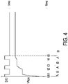
- FIG. 4 and FIG. 5 are exemplified to explain the precharge method for controlling the precharge system 1 of the present disclosure.
- S12 is the driving signal of the precharge switch 12
- Vbus is the bus voltage on the bus capacitor Cbus.
- the input switch 22 is controlled to be in the off state
- the precharge switch 12 is controlled to switch between the on state and the off state for multiple times.
- the load circuit 20 is in a work mode
- the input switch 22 is controlled to be in the on state.
- the precharge switch 12 may be controlled to be in the off state or the on state.
- the operation of the precharge system 1 during the load circuit 20 being in the precharge mode is described particularly as follows.
- the precharge switch 12 is turned on. During the time period from the timing t0 to t1, the precharge switch 12 is in the on state, the input current flows through the precharge resistor 11 and charges the bus capacitor Cbus, and thus the bus voltage Vbus increases. At the timing t1, the precharge switch 12 is turned off. During the time period from the timing t1 to t2, the precharge switch 12 is in the off state, the bus capacitor Cbus stops being charged, and the bus voltage Vbus is constant. In an embodiment, the bus voltage Vbus may decrease slightly. Please refer to FIG. 4 and FIG. 5. FIG.
- the consuming power of the precharge resistor 11 is equal to the limit power PI.
- the consuming power of the precharge switch 11 can be any value which is smaller than the limit power PI and is larger than a threshold power P2.
- the limit power PI is larger than the rated power of the precharge resistor 11.
- the thermal energy is gradually accumulated within the precharge resistor 11, which causes a permitted maximum of the consuming power of the precharge resistor 11 gradually decreases toward the threshold power P2. It is noted that the consuming power of the precharge resistor 11 is maintained to be larger than the threshold power P2 and to be smaller than or equal to the limit power PI during the time period from the timing t0 to t1. During the time period from the timing t1 to t2, the precharge switch 12 is in the off state, and the precharge resistor 11 stops working.
- the consuming power of the precharge resistor 11 is zero so that the precharge resistor 11 can dissipate heat for making itself return to be close to the initial status, and the permitted maximum of the consuming power of the precharge resistor 11 gradually increases toward the limit power PI.
- the permitted maximum of the consuming power of the precharge resistor 11 may return to equal the limit power PI.
- the consuming power of the precharge resistor 11 is equal to the limit power PI again.
- the consuming power of the precharge resistor 11 at the timing t2 may be any value which is slightly smaller than the limit power PI and is larger than the threshold power P2.
- the precharge switch 12 is in the on state, the bus capacitor Cbus is charged, the bus voltage Vbus increases, and the precharge resistor 11 works again.
- the thermal energy is gradually accumulated within the precharge resistor 11, which causes the permitted maximum of the consuming power of the precharge resistor 11 gradually decreases toward the threshold power P2 again.
- the consuming power of the precharge resistor 11 is maintained to be larger than the threshold power P2 and to be smaller than or equal to the limit power PI.
- the precharge switch 12 is in the off state, and the precharge resistor 11 stops working.
- the consuming power of the precharge resistor 11 is zero so that the precharge resistor 11 dissipates heat for making itself return to be close to the initial status again, namely the permitted maximum of the consuming power of the precharge resistor 11 gradually increases toward the limit power PI.
- the permitted maximum of the consuming power of the precharge resistor 11 may return to equal the limit power PI again.
- the bus capacitor Cbus stops being charged, and the bus voltage Vbus is constant. In an embodiment, the bus voltage Vbus may decrease slightly.
- the precharge switch 12 is in the on state, the bus capacitor Cbus is charged, and the bus voltage Vbus increases.
- the variation trend of the consuming power of the precharge resistor 11 during the time period from the timing t4 to t5 is the same as that during the time period from the timing t0 to t1 and the time period from the timing t2 to t3. It could be understood that the times of switching the precharge switch 12 between the on state and the off state during the load circuit 20 being in the precharge mode are not limited to that shown in FIG. 5 and can be adjusted according to actual requirements of the precharge system.
- the precharge resistor 11 works and gradually accumulates the thermal energy therein, and the permitted maximum of the consuming power of the precharge resistor 11 decreases gradually toward the threshold power P2.
- the time period B i.e., the time period from the timing t1 to t2, the time period from the timing t3 to t4, and the time period after the timing t5
- the precharge resistor 11 stops working and dissipates heat, and the permitted maximum of the consuming power of the precharge resistor 11 increases gradually toward the limit power PI.
- the permitted maximum of the consuming power of the precharge resistor 11 may return to equal the limit power P1. Therefore, through controlling the precharge switch 12 to switch between the on state and the off state, the precharge resistor 11 intermittently works with the consuming power which is larger than the threshold power P2 and is smaller than or equal to the limit power PI. Accordingly, when the precharge resistor 11 works, the consuming power of the precharge resistor 11 is maintained at a power level which is close to the limit power P1.
- the precharge system 1 is allowed to employ the precharge resistor 11 with low rated power so as to reduce the volume and cost of the precharge resistor 11, and it is faster for the precharge system 1 to complete the precharging. In addition, since the precharge resistor 11 dissipates heat intermittently, the reliability of the overall system is improved.
- the precharge method of the present disclosure it can be preset that the load circuit 20 in the precharge mode enters the work mode automatically while a specific condition is satisfied.
- the specific condition may be that the time length of the load circuit 20 being in the precharge mode reaches a preset time length, or that the times of switching the precharge switch 12 reach preset times, but not limited thereto.
- the precharge method of the present disclosure can determine whether to control the load circuit 20 in the precharge mode to enter the work mode in real time. The basis of determining whether to control the load circuit 20 in the precharge mode to enter the work mode is not limited and can be decided according to actual application environments and requirements.
- the bus voltage Vbus is detected in real time, and the load circuit 20 in the precharge mode is controlled to enter the work mode if the bus voltage Vbus is larger than or equal to a preset voltage.
- the precharge system 1 further comprises a voltage detector (not shown) electrically connected to the control circuit 30 and the bus capacitor Cbus.
- the accumulated time length of the precharge switch 12 being in the on state is accounted in real time, and the load circuit 20 in the precharge mode is controlled to enter the work mode if the accumulated time length is larger than or equal to a preset time length.
- a difference between the bus voltage Vbus and the input voltage on the input terminal 21 is calculated in real time, and the load circuit 20 in the precharge mode is controlled to enter the work mode if the difference is smaller than or equal to a preset value. Further, the timing and frequency of determining whether to control the load circuit 20 in the precharge mode to enter the work mode is not limited.
- the specific time length of the time periods A and B shown in FIG. 4 are not limited and only have to ensure that the consuming power of the precharge resistor 11 is always larger than the threshold power P2 and smaller than or equal to the limit power P1. It is noted that the time periods A and B only represent the time period of the precharge switch 12 being in the on state and the off state respectively, and it is unnecessary to make the time length of each time period A or B the same.
- the time length of the time periods A and B can be set in advance so as to simplify the switching control for the precharge switch 12, but not exclusively.
- the precharge method of the present disclosure can adjust the time length of each time period A or B in real time.
- the precharge method further comprises steps of detecting a temperature of the precharge resistor 11 and controlling the time length of the precharge switch 12 being in the on and off state according to the temperature of the precharge resistor 11.
- the precharge system 1 further comprises a temperature sensor (not shown) electrically connected to the control circuit 30 and the precharge circuit 10. The particular steps are described in detail as follows.
- the precharge switch 12 is controlled to be in the on state, and a first temperature of the precharge resistor 11 is detected. Then, the first temperature of the precharge resistor 11 is compared with a first threshold temperature, and the precharge switch 12 is controlled to switch from the on state to the off state if the first temperature of the precharge resistor 11 is larger than or equal to the first threshold temperature. Afterwards, the precharge switch 12 is maintained in the off state, and a second temperature of the precharge resistor 11 is detected. Then, the second temperature of the precharge resistor 11 is compared with a second threshold temperature, and the precharge switch 12 is controlled to switch from the off state to the on state if the second temperature of the precharge resistor 11 is smaller than or equal to the second threshold temperature. Finally, the above steps are repeated until the load circuit 20 in the precharge mode enters the work mode. In an embodiment, the first threshold temperature is higher than the second threshold temperature.
- the limit power PI of the precharge resistor 11 may vary dynamically.
- the limit power PI may be determined according to the type of the precharge resistor 11 and the time length of the precharge switch 12 being in the on state each time.
- the threshold power P2 when the precharge switch 12 switches between the on state and the off state, the threshold power P2 can be adjusted dynamically.
- the threshold power P2 may be determined according to the times of switching the precharge switch 12 between the on state and the off state, the time length of the precharge switch 12 being in the on state each time, the time length of the precharge switch 12 being in the off state each time, the temperature coefficient of the precharge resistor 11, and the condition of dissipating heat.
- the precharge method of the present disclosure is able to discover and shut down the system in time.
- the load circuit 20 under the circumstance that the load circuit 20 is in the precharge mode and the times of switching the precharge switch 12 between the on state and the off state is equal to preset times, if the bus voltage Vbus is smaller than a preset voltage and a difference between the bus voltage Vbus and the input voltage is larger than a preset value, the load circuit 20 in the precharge mode is controlled to enter a breakdown mode, and the precharge system 1 is shut down.
- FIG. 6 is a schematic flow chart illustrating a precharge method according to an embodiment of the present disclosure.
- the precharge method can be applied to the precharge system 1 described above.
- the input switch 22 is controlled to be in an off state
- the precharge switch 12 is controlled to switch between an on state and an off state for multiple times.
- a consuming power of the precharge resistor 11 is larger than a threshold power P2 and is smaller than or equal to a limit power PI of the precharge resistor 11, the input current flows through the precharge resistor 11 to charge the bus capacitor Cbus, and a bus voltage Vbus on the bus capacitor Cbus increases.
- the precharge switch 12 is in the off state, the consuming power of the precharge resistor 11 is zero, and the bus capacitor Cbus stops being charged.
- the input switch 22 is controlled to be in an on state.
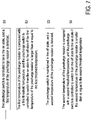
- the precharge method when the load circuit 20 is in the precharge mode, further comprises detecting a temperature of the precharge resistor 11, and controlling a time length of the precharge switch 12 being in the on state and the off state according to the temperature of the precharge resistor 11, which comprises the steps as shown in FIG. 7 .
- Step S1 the precharge switch 12 is controlled to be in the on state, and a first temperature of the precharge resistor 11 is detected.
- Step S2 the first temperature of the precharge resistor 11 is compared with a first threshold temperature, and the precharge switch 12 is controlled to switch from the on state to the off state if the first temperature of the precharge resistor 11 is larger than or equal to the first threshold temperature.
- Step S3 the precharge switch 12 is maintained in the off state, and a second temperature of the precharge resistor 11 is detected.
- Step S4 the second temperature of the precharge resistor 11 is compared with a second threshold temperature, and the precharge switch 12 is controlled to switch from the off state to the on state if the second temperature of the precharge resistor 11 is smaller than or equal to the second threshold temperature. The steps S1 to S4 are repeated until the load circuit 20 in the precharge mode enters the work mode.
- the present disclosure provides a precharge system and method.
- the precharge resistor Through controlling the precharge switch to switch between an on state and an off state, the precharge resistor intermittently works with a consuming power which is larger than a threshold power and is smaller than or equal to a limit power. Accordingly, when the precharge resistor works, the consuming power of the precharge resistor is maintained at a power level which is close to the limit power. Therefore, the precharge system is allowed to employ the precharge resistor with low rated power so as to reduce the volume and cost of the precharge resistor, and it is faster for the precharge system to complete the precharging. In addition, since the precharge resistor dissipates heat intermittently, the reliability of the overall system is improved.
Landscapes
- Engineering & Computer Science (AREA)
- Power Engineering (AREA)
- Direct Current Feeding And Distribution (AREA)
Abstract
Description
- The present disclosure relates to power electronical technology field, and more particularly to a precharge system and method.
- For avoiding the overcurrent phenomenon on bus capacitors during the start-up process, the precharge circuit is utilized to precharge the bus capacitor. Generally, the precharge circuit comprises a precharge switch and a precharge resistor. In the conventional precharge method, as shown in
FIG. 1 , during precharging the bus capacitor, the precharge switch is controlled to be turned on constantly for charging the bus capacitor continuously. After the bus voltage on the bus capacitor reaches a preset value or the precharge switch has been turned on for a preset time length, the precharge switch is turned off to finish the precharging. - However, during the precharging process, since the precharge switch is maintained in an on state, the precharge resistor works and consumes the power continuously. Moreover, as shown in
FIG. 2 , the overload ability of the resistor is inversely proportional to the time of the resistor working with load. Therefore, as the working time of the precharge resistor increases, the overload ability of the precharge resistor decreases gradually, namely the overload power of the precharge resistor decreases gradually. - Based on the conventional precharge method and the resistor characteristic stated above, the conventional precharge circuit has to employ the precharge resistor with large rated power. Accordingly, the type of the precharge resistor is limited, and the volume and cost of the precharge resistor are increased.
- Therefore, there is a need of providing a precharge system and method in order to overcome the drawbacks of the conventional technologies.
- The present disclosure provides a precharge system and method. Through controlling the precharge switch to switch between an on state and an off state for multiple times, the precharge resistor intermittently works with a consuming power which is close to a limit power. Therefore, the precharge system is allowed to employ the precharge resistor with low rated power so as to reduce the volume and cost of the precharge resistor, and it is faster for the precharge system to complete the precharging.
- In accordance with an aspect of the present disclosure, a precharge method configured to control a precharge system is provided. The precharge system comprises a load circuit and a precharge circuit, and the load circuit comprises an input terminal, an input switch and a bus capacitor. The input terminal is configured to receive an input current. The input switch is coupled between the input terminal and the bus capacitor. The precharge circuit is connected in parallel to the input switch and comprises a precharge resistor and a precharge switch connected in series. The precharge method comprises: during the load circuit being in a precharge mode, controlling the input switch to be in an off state, and controlling the precharge switch to switch between an on state and an off state for multiple times; and during the load circuit being in a work mode, controlling the input switch to be in an on state. During the load circuit being in the precharge mode, when the precharge switch is in the on state, a consuming power of the precharge resistor is larger than a threshold power and is smaller than or equal to a limit power of the precharge resistor, the input current flows through the precharge resistor to charge the bus capacitor, and a bus voltage on the bus capacitor increases. When the precharge switch is in the off state, the consuming power of the precharge resistor is zero, and the bus capacitor stops being charged.
- In accordance with another aspect of the present disclosure, a precharge system is provided. The precharge system comprises a load circuit, a precharge circuit and a control circuit, and the load circuit comprises an input terminal, an input switch and a bus capacitor. The input terminal is configured to receive an input current. The input switch is coupled between the input terminal and the bus capacitor. The precharge circuit is connected in parallel to the input switch and comprises a precharge resistor and a precharge switch connected in series. The control circuit is configured to perform the precharge method of the present disclosure.
- The present disclosure provides a precharge system and method. Through controlling the precharge switch to switch between an on state and an off state, the precharge resistor intermittently works with a consuming power which is larger than a threshold power and is smaller than or equal to a limit power. Accordingly, when the precharge resistor works, the consuming power of the precharge resistor is maintained at a power level which is close to the limit power. Therefore, the precharge system is allowed to employ the precharge resistor with low rated power so as to reduce the volume and cost of the precharge resistor, and it is faster for the precharge system to complete the precharging. In addition, since the precharge resistor dissipates heat intermittently, the reliability of the overall system is improved.
- The above contents of the present disclosure will become more readily apparent to those ordinarily skilled in the art after reviewing the following detailed description and accompanying drawings, in which:
-
-
FIG. 1 is a schematic oscillogram showing a waveform of bus capacitor and a switching sequence of precharge switch in the case of employing the conventional precharge method; -
FIG. 2 is a schematic view showing the relation between an overload power and a working time of a resistor; -
FIG. 3 is a schematic circuit diagram illustrating a precharge system according to an embodiment of the present disclosure; -
FIG. 4 is a schematic oscillogram showing waveforms of a driving signal of a precharge switch and a bus voltage ofFIG. 3 ; -
FIG. 5 is a schematic view showing the relation between the consuming power and the working time of the precharge resistor ofFIG. 3 ; -
FIGS. 6 and7 are schematic flow charts illustrating a precharge method according to an embodiment of the present disclosure. - The present disclosure will now be described more specifically with reference to the following embodiments. It is to be noted that the following descriptions of preferred embodiments of this disclosure are presented herein for purpose of illustration and description only. It is not intended to be exhaustive or to be limited to the precise form disclosed.
-
FIG. 3 is a schematic circuit diagram illustrating a precharge system according to an embodiment of the present disclosure. As shown inFIG. 3 , theprecharge system 1 comprises aprecharge circuit 10 and aload circuit 20, and theload circuit 20 comprises aninput terminal 21, aninput switch 22 and a bus capacitor Cbus. Theinput terminal 21 is configured to receive an input current. Theinput switch 22 is coupled between theinput terminal 21 and the bus capacitor Cbus. Theprecharge circuit 10 is connected in parallel to theinput switch 22, and theprecharge circuit 10 comprises aprecharge resistor 11 and aprecharge switch 12 connected in series. The input current can be a direct current, and the direct current is used to charge the bus capacitor Cbus. In an embodiment, the input current is an alternating current (i.e., theinput terminal 21 is connected to an alternating current source), and theload circuit 20 further comprises arectifier circuit 23. Therectifier circuit 23 is coupled between theinput switch 22 and the bus capacitor Cbus, and is configured to convert the alternating current into a direct current for charging the bus capacitor Cbus. InFIG. 3 , theload circuit 20 is exemplified as a two-phase circuit. In this embodiment, theload circuit 20 comprises twoinput switches 22, theprecharge system 1 comprises twoprecharge circuits 10, and the twoprecharge circuits 10 are connected in parallel to the twoinput switches 22 respectively. In fact, the number of phases of theload circuit 20 is not limited, theload circuit 20 is for example but not limited to a single-phase, two-phase or three-phase circuit. When the number of phases of theload circuit 20 changes, the number of theinput switch 22 and theprecharge circuit 10 changes accordingly. In addition, theprecharge system 1 further comprises acontrol circuit 30. Thecontrol circuit 30 is electrically connected to theload circuit 20 and theprecharge circuit 10 and is configured to control the operation of theprecharge system 1. It is noted that the precharge method described as follows in the present disclosure are all performed by thecontrol circuit 30 for controlling the operation of theprecharge system 1 accordingly. -
FIG. 4 andFIG. 5 are exemplified to explain the precharge method for controlling theprecharge system 1 of the present disclosure. InFIG. 4 , S12 is the driving signal of theprecharge switch 12, and Vbus is the bus voltage on the bus capacitor Cbus. As shown inFIG. 4 , during the time period from the timing t0 to t5, theload circuit 20 is in a precharge mode, theinput switch 22 is controlled to be in the off state, and theprecharge switch 12 is controlled to switch between the on state and the off state for multiple times. After the timing t5, theload circuit 20 is in a work mode, and theinput switch 22 is controlled to be in the on state. Further, when theload circuit 20 is in the work mode, theprecharge switch 12 may be controlled to be in the off state or the on state. The operation of theprecharge system 1 during theload circuit 20 being in the precharge mode is described particularly as follows. - At the timing t0, the
precharge switch 12 is turned on. During the time period from the timing t0 to t1, theprecharge switch 12 is in the on state, the input current flows through theprecharge resistor 11 and charges the bus capacitor Cbus, and thus the bus voltage Vbus increases. At the timing t1, theprecharge switch 12 is turned off. During the time period from the timing t1 to t2, theprecharge switch 12 is in the off state, the bus capacitor Cbus stops being charged, and the bus voltage Vbus is constant. In an embodiment, the bus voltage Vbus may decrease slightly. Please refer toFIG. 4 andFIG. 5. FIG. 5 is a schematic view showing the relation between the consuming power and the working time of theprecharge resistor 11, and the actual work region of theprecharge resistor 11 is illustrated by a shadow part inFIG. 5 . At the timing t0, the consuming power of theprecharge resistor 11 is equal to the limit power PI. In an embodiment, at the timing t0, the consuming power of theprecharge switch 11 can be any value which is smaller than the limit power PI and is larger than a threshold power P2. The limit power PI is larger than the rated power of theprecharge resistor 11. During the time period from the timing t0 to t1, theprecharge switch 12 is in the on state for allowing theprecharge resistor 11 to work. As the working time of theprecharge resistor 11 increases, the thermal energy is gradually accumulated within theprecharge resistor 11, which causes a permitted maximum of the consuming power of theprecharge resistor 11 gradually decreases toward the threshold power P2. It is noted that the consuming power of theprecharge resistor 11 is maintained to be larger than the threshold power P2 and to be smaller than or equal to the limit power PI during the time period from the timing t0 to t1. During the time period from the timing t1 to t2, theprecharge switch 12 is in the off state, and theprecharge resistor 11 stops working. Under this circumstance, the consuming power of theprecharge resistor 11 is zero so that theprecharge resistor 11 can dissipate heat for making itself return to be close to the initial status, and the permitted maximum of the consuming power of theprecharge resistor 11 gradually increases toward the limit power PI. In an embodiment, the permitted maximum of the consuming power of theprecharge resistor 11 may return to equal the limit power PI. - Afterwards, at the timing t2, the consuming power of the
precharge resistor 11 is equal to the limit power PI again. In an embodiment, the consuming power of theprecharge resistor 11 at the timing t2 may be any value which is slightly smaller than the limit power PI and is larger than the threshold power P2. During the time period from the timing t2 to t3, theprecharge switch 12 is in the on state, the bus capacitor Cbus is charged, the bus voltage Vbus increases, and theprecharge resistor 11 works again. As the working time of theprecharge resistor 11 increases, the thermal energy is gradually accumulated within theprecharge resistor 11, which causes the permitted maximum of the consuming power of theprecharge resistor 11 gradually decreases toward the threshold power P2 again. During the time period from the timing t2 to t3, the consuming power of theprecharge resistor 11 is maintained to be larger than the threshold power P2 and to be smaller than or equal to the limit power PI. During the time period from the timing t3 to t4, theprecharge switch 12 is in the off state, and theprecharge resistor 11 stops working. Under this circumstance, the consuming power of theprecharge resistor 11 is zero so that theprecharge resistor 11 dissipates heat for making itself return to be close to the initial status again, namely the permitted maximum of the consuming power of theprecharge resistor 11 gradually increases toward the limit power PI. In an embodiment, the permitted maximum of the consuming power of theprecharge resistor 11 may return to equal the limit power PI again. During the time period from the timing t3 to t4, the bus capacitor Cbus stops being charged, and the bus voltage Vbus is constant. In an embodiment, the bus voltage Vbus may decrease slightly. During the time period from the timing t4 to t5, theprecharge switch 12 is in the on state, the bus capacitor Cbus is charged, and the bus voltage Vbus increases. For the same reason, the variation trend of the consuming power of theprecharge resistor 11 during the time period from the timing t4 to t5 is the same as that during the time period from the timing t0 to t1 and the time period from the timing t2 to t3. It could be understood that the times of switching theprecharge switch 12 between the on state and the off state during theload circuit 20 being in the precharge mode are not limited to that shown inFIG. 5 and can be adjusted according to actual requirements of the precharge system. - From the above descriptions, during the time period A (i.e., the time period from the timing t0 to t1, the time period from the timing t2 to t3, and the time period from the timing t4 to t5), the
precharge resistor 11 works and gradually accumulates the thermal energy therein, and the permitted maximum of the consuming power of theprecharge resistor 11 decreases gradually toward the threshold power P2. During the time period B (i.e., the time period from the timing t1 to t2, the time period from the timing t3 to t4, and the time period after the timing t5), theprecharge resistor 11 stops working and dissipates heat, and the permitted maximum of the consuming power of theprecharge resistor 11 increases gradually toward the limit power PI. In an embodiment, the permitted maximum of the consuming power of theprecharge resistor 11 may return to equal the limit power P1. Therefore, through controlling theprecharge switch 12 to switch between the on state and the off state, theprecharge resistor 11 intermittently works with the consuming power which is larger than the threshold power P2 and is smaller than or equal to the limit power PI. Accordingly, when theprecharge resistor 11 works, the consuming power of theprecharge resistor 11 is maintained at a power level which is close to the limit power P1. By the precharge method of the present disclosure, theprecharge system 1 is allowed to employ theprecharge resistor 11 with low rated power so as to reduce the volume and cost of theprecharge resistor 11, and it is faster for theprecharge system 1 to complete the precharging. In addition, since theprecharge resistor 11 dissipates heat intermittently, the reliability of the overall system is improved. - In addition, in the precharge method of the present disclosure, it can be preset that the
load circuit 20 in the precharge mode enters the work mode automatically while a specific condition is satisfied. The specific condition may be that the time length of theload circuit 20 being in the precharge mode reaches a preset time length, or that the times of switching theprecharge switch 12 reach preset times, but not limited thereto. Moreover, the precharge method of the present disclosure can determine whether to control theload circuit 20 in the precharge mode to enter the work mode in real time. The basis of determining whether to control theload circuit 20 in the precharge mode to enter the work mode is not limited and can be decided according to actual application environments and requirements. For example, in an embodiment, the bus voltage Vbus is detected in real time, and theload circuit 20 in the precharge mode is controlled to enter the work mode if the bus voltage Vbus is larger than or equal to a preset voltage. Correspondingly, theprecharge system 1 further comprises a voltage detector (not shown) electrically connected to thecontrol circuit 30 and the bus capacitor Cbus. In another embodiment, the accumulated time length of theprecharge switch 12 being in the on state is accounted in real time, and theload circuit 20 in the precharge mode is controlled to enter the work mode if the accumulated time length is larger than or equal to a preset time length. In further another embodiment, a difference between the bus voltage Vbus and the input voltage on theinput terminal 21 is calculated in real time, and theload circuit 20 in the precharge mode is controlled to enter the work mode if the difference is smaller than or equal to a preset value. Further, the timing and frequency of determining whether to control theload circuit 20 in the precharge mode to enter the work mode is not limited. - Moreover, the specific time length of the time periods A and B shown in
FIG. 4 are not limited and only have to ensure that the consuming power of theprecharge resistor 11 is always larger than the threshold power P2 and smaller than or equal to the limit power P1. It is noted that the time periods A and B only represent the time period of theprecharge switch 12 being in the on state and the off state respectively, and it is unnecessary to make the time length of each time period A or B the same. - Furthermore, in the precharge method of the present disclosure, the time length of the time periods A and B can be set in advance so as to simplify the switching control for the
precharge switch 12, but not exclusively. In an embodiment, the precharge method of the present disclosure can adjust the time length of each time period A or B in real time. For example, when theload circuit 20 is in the precharge mode, the precharge method further comprises steps of detecting a temperature of theprecharge resistor 11 and controlling the time length of theprecharge switch 12 being in the on and off state according to the temperature of theprecharge resistor 11. Correspondingly, theprecharge system 1 further comprises a temperature sensor (not shown) electrically connected to thecontrol circuit 30 and theprecharge circuit 10. The particular steps are described in detail as follows. Firstly, theprecharge switch 12 is controlled to be in the on state, and a first temperature of theprecharge resistor 11 is detected. Then, the first temperature of theprecharge resistor 11 is compared with a first threshold temperature, and theprecharge switch 12 is controlled to switch from the on state to the off state if the first temperature of theprecharge resistor 11 is larger than or equal to the first threshold temperature. Afterwards, theprecharge switch 12 is maintained in the off state, and a second temperature of theprecharge resistor 11 is detected. Then, the second temperature of theprecharge resistor 11 is compared with a second threshold temperature, and theprecharge switch 12 is controlled to switch from the off state to the on state if the second temperature of theprecharge resistor 11 is smaller than or equal to the second threshold temperature. Finally, the above steps are repeated until theload circuit 20 in the precharge mode enters the work mode. In an embodiment, the first threshold temperature is higher than the second threshold temperature. - In an embodiment, when the
precharge switch 12 switches between the on state and the off state, the limit power PI of theprecharge resistor 11 may vary dynamically. The limit power PI may be determined according to the type of theprecharge resistor 11 and the time length of theprecharge switch 12 being in the on state each time. - In an embodiment, when the
precharge switch 12 switches between the on state and the off state, the threshold power P2 can be adjusted dynamically. The threshold power P2 may be determined according to the times of switching theprecharge switch 12 between the on state and the off state, the time length of theprecharge switch 12 being in the on state each time, the time length of theprecharge switch 12 being in the off state each time, the temperature coefficient of theprecharge resistor 11, and the condition of dissipating heat. - In addition, when the
precharge system 1 breaks down, the precharge method of the present disclosure is able to discover and shut down the system in time. For example, in an embodiment, under the circumstance that theload circuit 20 is in the precharge mode and the times of switching theprecharge switch 12 between the on state and the off state is equal to preset times, if the bus voltage Vbus is smaller than a preset voltage and a difference between the bus voltage Vbus and the input voltage is larger than a preset value, theload circuit 20 in the precharge mode is controlled to enter a breakdown mode, and theprecharge system 1 is shut down. -
FIG. 6 is a schematic flow chart illustrating a precharge method according to an embodiment of the present disclosure. The precharge method can be applied to theprecharge system 1 described above. In the precharge method, as shown inFIG. 6 , during theload circuit 20 being in a precharge mode, theinput switch 22 is controlled to be in an off state, and theprecharge switch 12 is controlled to switch between an on state and an off state for multiple times. In particular, when theprecharge switch 12 is in the on state, a consuming power of theprecharge resistor 11 is larger than a threshold power P2 and is smaller than or equal to a limit power PI of theprecharge resistor 11, the input current flows through theprecharge resistor 11 to charge the bus capacitor Cbus, and a bus voltage Vbus on the bus capacitor Cbus increases. When theprecharge switch 12 is in the off state, the consuming power of theprecharge resistor 11 is zero, and the bus capacitor Cbus stops being charged. In addition, during theload circuit 20 being in a work mode, theinput switch 22 is controlled to be in an on state. - In an embodiment, when the
load circuit 20 is in the precharge mode, the precharge method further comprises detecting a temperature of theprecharge resistor 11, and controlling a time length of theprecharge switch 12 being in the on state and the off state according to the temperature of theprecharge resistor 11, which comprises the steps as shown inFIG. 7 . Firstly, in Step S1, theprecharge switch 12 is controlled to be in the on state, and a first temperature of theprecharge resistor 11 is detected. Then, in Step S2, the first temperature of theprecharge resistor 11 is compared with a first threshold temperature, and theprecharge switch 12 is controlled to switch from the on state to the off state if the first temperature of theprecharge resistor 11 is larger than or equal to the first threshold temperature. Then, in Step S3, theprecharge switch 12 is maintained in the off state, and a second temperature of theprecharge resistor 11 is detected. Finally, in Step S4, the second temperature of theprecharge resistor 11 is compared with a second threshold temperature, and theprecharge switch 12 is controlled to switch from the off state to the on state if the second temperature of theprecharge resistor 11 is smaller than or equal to the second threshold temperature. The steps S1 to S4 are repeated until theload circuit 20 in the precharge mode enters the work mode. - In summary, the present disclosure provides a precharge system and method. Through controlling the precharge switch to switch between an on state and an off state, the precharge resistor intermittently works with a consuming power which is larger than a threshold power and is smaller than or equal to a limit power. Accordingly, when the precharge resistor works, the consuming power of the precharge resistor is maintained at a power level which is close to the limit power. Therefore, the precharge system is allowed to employ the precharge resistor with low rated power so as to reduce the volume and cost of the precharge resistor, and it is faster for the precharge system to complete the precharging. In addition, since the precharge resistor dissipates heat intermittently, the reliability of the overall system is improved.
Claims (14)
- A precharge method configured to control a precharge system (1), wherein the precharge system (1) comprises a load circuit (20) and a precharge circuit (10), the load circuit (20) comprises an input terminal (21), an input switch (22) and a bus capacitor (Cbus), the input terminal (21) is configured to receive an input current, the input switch (22) is coupled between the input terminal (21) and the bus capacitor (Cbus), the precharge circuit (10) is connected in parallel to the input switch (22) and comprises a precharge resistor (11) and a precharge switch (12) connected in series, and the precharge method is characterized by comprising:during the load circuit (20) being in a precharge mode, controlling the input switch (22) to be in an off state, and controlling the precharge switch (12) to switch between an on state and an off state for multiple times, wherein when the precharge switch (12) is in the on state, a consuming power of the precharge resistor (11) is larger than a threshold power (P2) and is smaller than or equal to a limit power (PI) of the precharge resistor (11), the input current flows through the precharge resistor (11) to charge the bus capacitor (Cbus), and a bus voltage (Vbus) on the bus capacitor (Cbus) increases, and when the precharge switch (12) is in the off state, the consuming power of the precharge resistor (11) is zero, and the bus capacitor (Cbus) stops being charged; andduring the load circuit (20) being in a work mode, controlling the input switch (22) to be in an on state.
- The precharge method according to claim 1, wherein when the load circuit (20) is in the precharge mode, the precharge method further comprises:detecting a temperature of the precharge resistor (11); andcontrolling a time length of the precharge switch (12) being in the on state and the off state according to the temperature of the precharge resistor (11).
- The precharge method according to claim 2, wherein controlling the time length of the precharge switch (12) being in the on state and the off state according to the temperature of the precharge resistor (11) comprises steps of:(S1) controlling the precharge switch (12) to be in the on state, and detecting a first temperature of the precharge resistor (11);(S2) comparing the first temperature of the precharge resistor (11) with a first threshold temperature, and controlling the precharge switch (12) to switch from the on state to the off state if the first temperature of the precharge resistor (11) being larger than or equal to the first threshold temperature;(S3) maintaining the precharge switch (12) in the off state, and detecting a second temperature of the precharge resistor (11);(S4) comparing the second temperature of the precharge resistor (11) with a second threshold temperature, and controlling the precharge switch (12) to switch from the off state to the on state if the second temperature of the precharge resistor (11) being smaller than or equal to the second threshold temperature; and(S5) repeating the steps S1 to S4 until the load circuit (20) in the precharge mode entering the work mode.
- The precharge method according to claim 3, wherein the first threshold temperature is larger than the second threshold temperature.
- The precharge method according to claim 1, wherein when the precharge switch (12) is controlled to switch between the on state and the off state, the limit power (PI) varies dynamically.
- The precharge method according to claim 5, wherein the limit power (PI) is determined according to a type of the precharge resistor (11) and a time length of the precharge switch (12) being in the on state each time.
- The precharge method according to claim 1, wherein when the precharge switch (12) is controlled to switch between the on state and the off state, the threshold power (P2) is adjusted dynamically.
- The precharge method according to claim 7, wherein the threshold power (P2) is determined according to the times of switching the precharge switch (12) between the on state and the off state, a time length of the precharge switch (12) being in the on state each time, a time length of the precharge switch (12) being in the off state each time, a temperature coefficient of the precharge resistor (11), and a condition of dissipating heat.
- The precharge method according to claim 1, wherein when the load circuit (20) is in the precharge mode, the bus voltage (Vbus) is detected in real time, and the load circuit (20) in the precharge mode is controlled to enter the work mode if the bus voltage (Vbus) is larger than or equal to a preset voltage.
- The precharge method according to claim 1, wherein when the load circuit (20) is in the precharge mode, an accumulated time length of the precharge switch (12) being in the on state is accounted in real time, and the load circuit (20) in the precharge mode is controlled to enter the work mode if the accumulated time length is larger than or equal to a preset time length.
- The precharge method according to claim 1, wherein when the load circuit (20) is in the precharge mode, a difference between the bus voltage (Vbus) and an input voltage is calculated in real time, and the load circuit (20) in the precharge mode is controlled to enter the work mode if the difference is smaller than or equal to a preset value.
- The precharge method according to claim 1, wherein under a circumstance that the load circuit (20) is in the precharge mode and the times of switching the precharge switch (12) between the on state and the off state is equal to preset times, if the bus voltage (Vbus) is smaller than a preset voltage and a difference between the bus voltage (Vbus) and an input voltage is larger than a preset value, the load circuit (20) in the precharge mode is controlled to enter a breakdown mode, and the precharge system (1) is shut down.
- The precharge method according to claim 1, wherein the limit power (PI) of the precharge resistor (11) is larger than a rated power of the precharge resistor (11).
- A precharge system (1), characterized by comprising a load circuit (20), a precharge circuit (10) and a control circuit (30), wherein the load circuit (20) comprises an input terminal (21), an input switch (22) and a bus capacitor (Cbus), the input terminal (21) is configured to receive an input current, the input switch (22) is coupled between the input terminal (21) and the bus capacitor (Cbus), the precharge circuit (10) is connected in parallel to the input switch (22) and comprises a precharge resistor (11) and a precharge switch (12) connected in series, and the control circuit (30) is configured to perform the precharge method according to any of claims 1-13.
Applications Claiming Priority (1)
| Application Number | Priority Date | Filing Date | Title |
|---|---|---|---|
| CN202110710247.2A CN115528898A (en) | 2021-06-25 | 2021-06-25 | Pre-charging system and method |
Publications (1)
| Publication Number | Publication Date |
|---|---|
| EP4109727A1 true EP4109727A1 (en) | 2022-12-28 |
Family
ID=78621684
Family Applications (1)
| Application Number | Title | Priority Date | Filing Date |
|---|---|---|---|
| EP21206144.4A Pending EP4109727A1 (en) | 2021-06-25 | 2021-11-03 | Precharge system and method |
Country Status (3)
| Country | Link |
|---|---|
| US (1) | US11777402B2 (en) |
| EP (1) | EP4109727A1 (en) |
| CN (1) | CN115528898A (en) |
Citations (1)
| Publication number | Priority date | Publication date | Assignee | Title |
|---|---|---|---|---|
| EP3700053A1 (en) * | 2019-02-21 | 2020-08-26 | Commissariat à l'énergie atomique et aux énergies alternatives | System and method of preloading of a capacitor by a battery comprising a preloading resistance and a chopper device |
Family Cites Families (13)
| Publication number | Priority date | Publication date | Assignee | Title |
|---|---|---|---|---|
| US7528574B1 (en) * | 2006-02-16 | 2009-05-05 | Summit Microelectronics, Inc. | Systems and methods of programming voltage and current in a battery charger |
| JP5127387B2 (en) * | 2007-10-01 | 2013-01-23 | 三洋電機株式会社 | Power supply for vehicle |
| US8000671B2 (en) * | 2008-04-01 | 2011-08-16 | Seiko Epson Corporation | Dual threshold demodulation in an amplitude modulation radio receiver |
| DE102009037723B4 (en) * | 2009-08-17 | 2016-08-11 | Siemens Aktiengesellschaft | Method for discharging a link capacitor of a voltage source inverter |
| EP2523333B1 (en) * | 2011-05-11 | 2019-09-11 | Siemens Aktiengesellschaft | Method for operating of a frequency inverter with a regulated pre-charge |
| FR3017754B1 (en) * | 2014-02-14 | 2018-04-27 | Commissariat A L'energie Atomique Et Aux Energies Alternatives | CONTINUOUS VOLTAGE SUPPLY SYSTEM CONFIGURED TO PRECHARGE A FILTER CAPACITOR BEFORE FEEDING A LOAD |
| CN206628973U (en) | 2017-02-23 | 2017-11-10 | 国网江西省电力公司赣东北供电分公司 | A kind of low-voltage transverter soft starting circuit of small dash current |
| US10027223B1 (en) * | 2017-06-12 | 2018-07-17 | Linear Technology Holding Llc | Soft-charging of switched capacitors in power converter circuits |
| CN111289870B (en) | 2018-12-06 | 2022-12-06 | 中车时代电动汽车股份有限公司 | A pre-charging circuit fault detection method and device thereof |
| JP7120072B2 (en) * | 2019-02-22 | 2022-08-17 | 株式会社デンソー | Precharge controller |
| JP7371126B2 (en) * | 2019-05-31 | 2023-10-30 | 広東美的制冷設備有限公司 | Drive control method, drive control device, home appliance and computer readable storage medium |
| CN110829817B (en) * | 2019-11-18 | 2022-02-11 | 广东美的暖通设备有限公司 | Control circuit, control method and device of control circuit and air conditioner |
| CN112865577B (en) * | 2021-01-29 | 2023-04-18 | 重庆大学 | Pre-charging circuit of hybrid multi-level converter (HCC) and control method thereof |
-
2021
- 2021-06-25 CN CN202110710247.2A patent/CN115528898A/en active Pending
- 2021-10-06 US US17/494,998 patent/US11777402B2/en active Active
- 2021-11-03 EP EP21206144.4A patent/EP4109727A1/en active Pending
Patent Citations (1)
| Publication number | Priority date | Publication date | Assignee | Title |
|---|---|---|---|---|
| EP3700053A1 (en) * | 2019-02-21 | 2020-08-26 | Commissariat à l'énergie atomique et aux énergies alternatives | System and method of preloading of a capacitor by a battery comprising a preloading resistance and a chopper device |
Also Published As
| Publication number | Publication date |
|---|---|
| US11777402B2 (en) | 2023-10-03 |
| CN115528898A (en) | 2022-12-27 |
| US20220416647A1 (en) | 2022-12-29 |
Similar Documents
| Publication | Publication Date | Title |
|---|---|---|
| US8174802B2 (en) | Switching regulator and operations control method thereof | |
| US6275399B1 (en) | Method and apparatus for driving a semiconductor element with variable resistance circuitry | |
| US6271709B1 (en) | Gate drive circuit of voltage drive switching element | |
| CN110224592B (en) | Multiphase critical conduction power converter and control method thereof | |
| US12040707B2 (en) | Step-up circuit and step-up circuit control method | |
| US6556457B1 (en) | Method of controlling inverter power generation apparatus | |
| US6462924B1 (en) | Power supply apparatus comprising a voltage detection circuit and method for using same | |
| US6317339B1 (en) | Method of controlling electric power supply apparatus with electric power converter circuit | |
| US6756756B1 (en) | Phase detector motor start switch | |
| US11777402B2 (en) | Precharge system and method | |
| US6366058B1 (en) | Capacitor power supply unit | |
| JP3372914B2 (en) | Switching power supply | |
| EP1693949B1 (en) | Electric power converter apparatus | |
| US20060114700A1 (en) | Method for controlling the transient response of a power converter powering a load, transient response controller and power converter | |
| JP2001078447A (en) | Switching power circuit | |
| EP4340195B1 (en) | POWER REFERENCER CONTROL DEVICE, POWER REFERENCER AND METHOD FOR OPERATION OF A POWER REFERENCER | |
| CN113424423A (en) | Double step-down chopper circuit | |
| US20240388207A1 (en) | Isolated switching converter with adaptive driving strength and control method thereof | |
| JPS6377383A (en) | Starting circuit | |
| JPH0530755A (en) | Discharge circuit of inverter device | |
| US11949341B2 (en) | Power converter and electric motor braking method | |
| JP2022064560A (en) | Power supply device | |
| JPH073833Y2 (en) | Overcurrent protection circuit for switching power supply | |
| CN121602972A (en) | Switching circuit with gentle start and switching control circuit and method | |
| CN120902648A (en) | V2L converter for vehicle and method of controlling the same |
Legal Events
| Date | Code | Title | Description |
|---|---|---|---|
| PUAI | Public reference made under article 153(3) epc to a published international application that has entered the european phase |
Free format text: ORIGINAL CODE: 0009012 |
|
| STAA | Information on the status of an ep patent application or granted ep patent |
Free format text: STATUS: THE APPLICATION HAS BEEN PUBLISHED |
|
| AK | Designated contracting states |
Kind code of ref document: A1 Designated state(s): AL AT BE BG CH CY CZ DE DK EE ES FI FR GB GR HR HU IE IS IT LI LT LU LV MC MK MT NL NO PL PT RO RS SE SI SK SM TR |
|
| STAA | Information on the status of an ep patent application or granted ep patent |
Free format text: STATUS: REQUEST FOR EXAMINATION WAS MADE |
|
| 17P | Request for examination filed |
Effective date: 20230622 |
|
| RBV | Designated contracting states (corrected) |
Designated state(s): AL AT BE BG CH CY CZ DE DK EE ES FI FR GB GR HR HU IE IS IT LI LT LU LV MC MK MT NL NO PL PT RO RS SE SI SK SM TR |