EP4109675A1 - Antenna structure, radar and terminal - Google Patents
Antenna structure, radar and terminal Download PDFInfo
- Publication number
- EP4109675A1 EP4109675A1 EP20926204.7A EP20926204A EP4109675A1 EP 4109675 A1 EP4109675 A1 EP 4109675A1 EP 20926204 A EP20926204 A EP 20926204A EP 4109675 A1 EP4109675 A1 EP 4109675A1
- Authority
- EP
- European Patent Office
- Prior art keywords
- patch unit
- patch
- unit group
- antenna structure
- main feeder
- Prior art date
- Legal status (The legal status is an assumption and is not a legal conclusion. Google has not performed a legal analysis and makes no representation as to the accuracy of the status listed.)
- Granted
Links
Images




Classifications
-
- H—ELECTRICITY
- H01—ELECTRIC ELEMENTS
- H01Q—ANTENNAS, i.e. RADIO AERIALS
- H01Q21/00—Antenna arrays or systems
- H01Q21/06—Arrays of individually energised antenna units similarly polarised and spaced apart
- H01Q21/061—Two dimensional planar arrays
- H01Q21/065—Patch antenna array
-
- H—ELECTRICITY
- H01—ELECTRIC ELEMENTS
- H01Q—ANTENNAS, i.e. RADIO AERIALS
- H01Q3/00—Arrangements for changing or varying the orientation or the shape of the directional pattern of the waves radiated from an antenna or antenna system
- H01Q3/22—Arrangements for changing or varying the orientation or the shape of the directional pattern of the waves radiated from an antenna or antenna system varying the orientation in accordance with variation of frequency of radiated wave
-
- H—ELECTRICITY
- H01—ELECTRIC ELEMENTS
- H01Q—ANTENNAS, i.e. RADIO AERIALS
- H01Q9/00—Electrically-short antennas having dimensions not more than twice the operating wavelength and consisting of conductive active radiating elements
- H01Q9/04—Resonant antennas
- H01Q9/0407—Substantially flat resonant element parallel to ground plane, e.g. patch antenna
-
- G—PHYSICS
- G01—MEASURING; TESTING
- G01S—RADIO DIRECTION-FINDING; RADIO NAVIGATION; DETERMINING DISTANCE OR VELOCITY BY USE OF RADIO WAVES; LOCATING OR PRESENCE-DETECTING BY USE OF THE REFLECTION OR RERADIATION OF RADIO WAVES; ANALOGOUS ARRANGEMENTS USING OTHER WAVES
- G01S7/00—Details of systems according to groups G01S13/00, G01S15/00, G01S17/00
- G01S7/02—Details of systems according to groups G01S13/00, G01S15/00, G01S17/00 of systems according to group G01S13/00
- G01S7/03—Details of HF subsystems specially adapted therefor, e.g. common to transmitter and receiver
- G01S7/032—Constructional details for solid-state radar subsystems
-
- H—ELECTRICITY
- H01—ELECTRIC ELEMENTS
- H01Q—ANTENNAS, i.e. RADIO AERIALS
- H01Q1/00—Details of, or arrangements associated with, antennas
- H01Q1/12—Supports; Mounting means
- H01Q1/22—Supports; Mounting means by structural association with other equipment or articles
-
- H—ELECTRICITY
- H01—ELECTRIC ELEMENTS
- H01Q—ANTENNAS, i.e. RADIO AERIALS
- H01Q1/00—Details of, or arrangements associated with, antennas
- H01Q1/27—Adaptation for use in or on movable bodies
- H01Q1/32—Adaptation for use in or on road or rail vehicles
- H01Q1/3208—Adaptation for use in or on road or rail vehicles characterised by the application wherein the antenna is used
- H01Q1/3233—Adaptation for use in or on road or rail vehicles characterised by the application wherein the antenna is used particular used as part of a sensor or in a security system, e.g. for automotive radar, navigation systems
-
- H—ELECTRICITY
- H01—ELECTRIC ELEMENTS
- H01Q—ANTENNAS, i.e. RADIO AERIALS
- H01Q1/00—Details of, or arrangements associated with, antennas
- H01Q1/36—Structural form of radiating elements, e.g. cone, spiral, umbrella; Particular materials used therewith
-
- H—ELECTRICITY
- H01—ELECTRIC ELEMENTS
- H01Q—ANTENNAS, i.e. RADIO AERIALS
- H01Q1/00—Details of, or arrangements associated with, antennas
- H01Q1/50—Structural association of antennas with earthing switches, lead-in devices or lightning protectors
-
- H—ELECTRICITY
- H01—ELECTRIC ELEMENTS
- H01Q—ANTENNAS, i.e. RADIO AERIALS
- H01Q13/00—Waveguide horns or mouths; Slot antennas; Leaky-waveguide antennas; Equivalent structures causing radiation along the transmission path of a guided wave
- H01Q13/20—Non-resonant leaky-waveguide or transmission-line antennas; Equivalent structures causing radiation along the transmission path of a guided wave
- H01Q13/206—Microstrip transmission line antennas
-
- H—ELECTRICITY
- H01—ELECTRIC ELEMENTS
- H01Q—ANTENNAS, i.e. RADIO AERIALS
- H01Q21/00—Antenna arrays or systems
- H01Q21/06—Arrays of individually energised antenna units similarly polarised and spaced apart
-
- H—ELECTRICITY
- H01—ELECTRIC ELEMENTS
- H01Q—ANTENNAS, i.e. RADIO AERIALS
- H01Q5/00—Arrangements for simultaneous operation of antennas on two or more different wavebands, e.g. dual-band or multi-band arrangements
- H01Q5/30—Arrangements for providing operation on different wavebands
- H01Q5/307—Individual or coupled radiating elements, each element being fed in an unspecified way
- H01Q5/342—Individual or coupled radiating elements, each element being fed in an unspecified way for different propagation modes
- H01Q5/357—Individual or coupled radiating elements, each element being fed in an unspecified way for different propagation modes using a single feed point
- H01Q5/364—Creating multiple current paths
- H01Q5/371—Branching current paths
-
- G—PHYSICS
- G01—MEASURING; TESTING
- G01S—RADIO DIRECTION-FINDING; RADIO NAVIGATION; DETERMINING DISTANCE OR VELOCITY BY USE OF RADIO WAVES; LOCATING OR PRESENCE-DETECTING BY USE OF THE REFLECTION OR RERADIATION OF RADIO WAVES; ANALOGOUS ARRANGEMENTS USING OTHER WAVES
- G01S13/00—Systems using the reflection or reradiation of radio waves, e.g. radar systems; Analogous systems using reflection or reradiation of waves whose nature or wavelength is irrelevant or unspecified
- G01S13/88—Radar or analogous systems specially adapted for specific applications
- G01S13/93—Radar or analogous systems specially adapted for specific applications for anti-collision purposes
- G01S13/931—Radar or analogous systems specially adapted for specific applications for anti-collision purposes of land vehicles
-
- G—PHYSICS
- G01—MEASURING; TESTING
- G01S—RADIO DIRECTION-FINDING; RADIO NAVIGATION; DETERMINING DISTANCE OR VELOCITY BY USE OF RADIO WAVES; LOCATING OR PRESENCE-DETECTING BY USE OF THE REFLECTION OR RERADIATION OF RADIO WAVES; ANALOGOUS ARRANGEMENTS USING OTHER WAVES
- G01S7/00—Details of systems according to groups G01S13/00, G01S15/00, G01S17/00
- G01S7/02—Details of systems according to groups G01S13/00, G01S15/00, G01S17/00 of systems according to group G01S13/00
- G01S7/03—Details of HF subsystems specially adapted therefor, e.g. common to transmitter and receiver
Definitions
- This application relates to the field of sensor technologies, and more specifically, to an antenna structure, a radar, and a terminal in the field of sensor technologies.
- a sensor plays a very important role in unmanned driving and intelligent driving of an intelligent vehicle.
- the sensor may be a millimeter-wave radar, a laser radar, an ultrasonic radar, a camera, or the like.
- a 77 GHz millimeter-wave radar has features such as a short wavelength and a small device size.
- the 77 GHz millimeter-wave radar has irreplaceable advantages in terms of detection precision, detection distance, and device integration.
- an antenna used by the radar is required to have a wide 3 dB beam bandwidth and a low sidelobe.
- the wide 3 dB beam bandwidth can ensure a large detection angle range in a horizontal direction, and the low sidelobe can reduce clutter energy reflected by the ground in a vertical direction. Consequently, a false alarm probability is reduced.
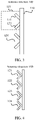
- FIG. 1 is a schematic diagram of a structure of an existing antenna structure.
- the existing antenna structure uses a series-feed mode, that is, a plurality of radiation patches that are vertically connected to a feeder are simultaneously excited by using one feeder. Widths of the plurality of radiation patches first gradually increase and then gradually decrease in a length direction of the feeder, that is, energy radiated by the antenna structure is concentrated in a middle area close to a length of the feeder, so that low sidelobe weighting can be implemented. This avoids radar false alarm.
- the existing antenna structure shown in FIG. 1 may implement a low sidelobe level, but has a small 3 dB beam width. This leads to a small detection angle range in the horizontal direction.
- Embodiments of this application provide an antenna structure, a radar, and a terminal, to extend a 3 dB bandwidth of the antenna structure.
- an embodiment of this application provides an antenna structure.
- the antenna structure includes a main feeder and at least one patch unit group.
- the at least one patch unit group is connected in series to the main feeder in a length direction of the main feeder.
- Each of the at least one patch unit group includes at least two patch units disposed in a V-shaped structure.
- Each patch unit group is connected in series to the main feeder through the two patch units that are disposed in the V-shaped structure and that are in each patch unit group.
- each patch unit group is connected in series to the main feeder through the two patch units that are disposed in the V-shaped structure and that are in each patch unit group. Because an included angle exists between the two patch units in the V-shaped structure, an aperture of the antenna structure can be reduced by adjusting the included angle. This can extend a 3 dB bandwidth of the antenna structure.
- the at least one patch unit group includes a plurality of patch unit groups for description.
- each patch unit group may be connected in series to the main feeder through the two patch units that are disposed in the V-shaped structure and that are in each patch unit group in a plurality of manners. This is not limited in this embodiment of this application.
- each patch unit group is connected in series to the main feeder through a connection point of the two patch units that are disposed in the V-shaped structure and that are in each patch unit group.
- each patch unit group may be connected in series to the main feeder through a partial region of each of the two patch units that are disposed in the V-shaped structure and that are in each patch unit group.
- the plurality of patch unit groups may be connected in series to the main feeder in a plurality of manners. This is not limited in this embodiment of this application.
- the plurality of patch unit groups may be connected in series to a same side of the main feeder.
- the plurality of patch unit groups may be connected in series to two sides of the main feeder.
- a case in which the plurality of patch units are connected in series to the two sides of the main feeder can increase a horizontal radiation range.
- the plurality of patch unit groups may be connected in series to the two sides of the main feeder in a plurality of manners. This is not limited in this embodiment of this application.
- the plurality of patch unit groups are alternately connected in series to two sides of the main feeder.
- some of the plurality of patch unit groups may be sequentially connected in series to one side of the main feeder, and the rest of patch unit groups may be sequentially connected in series to the other side of the main feeder.
- an interval between the patch unit groups when the plurality of patch unit groups are connected in series to the two sides of the main feeder is shorter than an interval between the patch unit groups when the plurality of patch unit groups are connected in series to the same side of the main feeder.
- the plurality of patch unit groups are connected in series to two sides of the main feeder, so that a size of the main feeder can be reduced.
- an interval between the patch unit groups when the plurality of patch unit groups are alternately connected in series to two sides of the main feeder is shorter than an interval between the patch unit groups when some of the plurality of patch unit groups are first connected in series to one side of the main feeder, and the other of patch unit groups are then connected in series to the other side of the main feeder, and an interval between the patch unit groups when the plurality of patch unit groups are connected in series to the same side of the main feeder. Therefore, the plurality of patch unit groups are alternately connected in series to two sides of the main feeder, so that a size of the main feeder can be reduced.
- widths of the patch units in each patch unit group may be set to different values. This is not limited in this embodiment of this application.
- a width of a patch unit in the plurality of patch unit groups first increases and then decreases in a first direction.
- a width of a patch unit in the plurality of patch unit groups increases or decreases in a first direction.
- a width of a patch unit in the plurality of patch unit groups is the same.
- widths of patch units in different patch unit groups may be the same or may be different. This is not limited in this embodiment of this application.
- widths of the patch units in the different patch unit groups are the same includes being exactly the same and being approximately the same, where being approximately the same means that a difference between the widths of the patch units in the different patch unit groups is within a specific error range.
- the widths of the patch units in the patch unit group are designed, so that requirements for different electromagnetic wave radiation shapes can be met. For example, when the width of the patch unit designed in the foregoing first possible implementation is used, because energy is concentrated in a middle segment of the main feeder, a low sidelobe can be implemented. This reduces a false alarm probability.
- an included angle between two patch units that are disposed in a V shape and that are in each patch unit group and an included angle between each patch unit group and the main feeder may be of different sizes. This is not limited in this embodiment of this application.
- the included angle between the two patch units in each patch unit group may be 90°.
- the included angle between each patch unit group and the main feeder may be 45°.
- the included angle between the two patch units that are disposed in the V-shaped structure and that are in each patch unit is set, so that different aperture requirements of the antenna structure can be met, a horizontal beam width of an antenna can be further broadened, and a low sidelobe requirement of a vertical plane can be further implemented.
- lengths of the patch units in each patch unit group may be set to be of different sizes. This is not limited in this embodiment of this application.
- lengths of the patch units in the plurality of patch unit groups first increase and then decrease in a first direction.
- lengths of the patch units in the plurality of patch unit groups increase or decrease in a first direction.
- lengths of the patch units in the plurality of patch unit groups are the same.
- lengths of the patch units in different patch unit groups may be the same or may be different. This is not limited in this embodiment of this application.
- the lengths of the patch units in the different patch unit groups are the same includes being exactly the same and being approximately the same, where being approximately the same means that a difference between the lengths of the patch units in the different patch unit groups is within a specific error range.
- a size of a patch unit in each patch unit group includes a length and a width.
- sizes of patch units in different patch unit groups may be the same or may be different. This is not limited in this embodiment of this application.
- the sizes of the patch units in the different patch unit groups are the same includes being exactly the same and being approximately the same, where being approximately the same means that a difference between the sizes of the patch units in the different patch unit groups is within a specific error range.
- each patch unit group includes two patch units disposed in a V-shaped structure may be understood as follows: The two patch units are disposed in a V-shaped structure, or the two patch units are disposed in a similar V-shaped structure. This is not limited in this embodiment of this application.
- each patch unit group may be of a C-shaped structure.
- the two patch units included in each patch unit group may be of an L-shaped structure.
- the patch unit in each patch unit group may be rectangular.
- the patch unit in each patch unit group may be in the shape of a polygon, for example, a parallelogram.
- shapes of the patch units in each patch unit group may be the same or may be different. This is not limited in this embodiment of this application.
- the antenna structure may operate in a standing wave mode or a traveling wave mode. This is not limited in this embodiment of this application.
- a first end of the antenna structure when the antenna structure operates in the standing wave mode, a first end of the antenna structure does not include a load matching unit.
- a first end of the antenna structure does not include a load matching unit may be understood as that the first end of the antenna structure is open-circuited.
- a second end of the antenna structure when the antenna structure operates in the traveling wave mode, a second end of the antenna structure further includes a load matching unit.
- the load matching unit is configured to consume energy that is not consumed totally by the at least one patch unit group.
- the load matching unit may be connected to the first end of the main feeder in a plurality of manners. This is not limited in this embodiment of this application.
- the load matching unit is in a same length direction as the main feeder.
- the load matching unit is connected to the main feeder by bending.
- an embodiment of this application further provides a radar.
- the radar includes the antenna structure according to any one of the first aspect or the possible implementations of the first aspect.
- the radar further includes a control chip.
- the control chip is connected to a second end of the antenna structure.
- the control chip is configured to control the antenna structure to transmit or receive a signal.
- control chip may be connected to the second end of the antenna structure through a first microstrip line.
- the radar further includes an impedance matching unit.
- the impedance matching unit is configured to match impedance of the second end with impedance of the control chip, and the control chip is connected to the second end through the impedance matching unit.
- the impedance matching unit may be a second microstrip line.
- the impedance of the second end of the antenna structure can match the impedance of the control chip by adjusting impedance of the second microstrip line.
- the radar further includes a printed circuit board.
- the printed circuit board includes the antenna structure, a dielectric layer, and a metal layer that are sequentially disposed in a stacked manner.
- the antenna structure is grounded through the metal layer.
- an embodiment of this application further provides a terminal.
- the terminal includes the radar according to the second aspect or the possible implementations of the second aspect.
- the terminal in this embodiment of this application may have a capability of implementing a communication function and/or a detection function through a radar. This is not limited in this embodiment of this application.
- the terminal may be a vehicle, an unmanned aerial vehicle, an unmanned transport vehicle, a robot, or the like in self-driving or intelligent driving.
- the terminal may be a mobile phone, a tablet computer, a computer with a wireless transceiver function, a virtual reality terminal, an augmented reality terminal, a wireless terminal in industrial control, a wireless terminal in unmanned driving, a wireless terminal in telemedicine, a wireless terminal in a smart grid, a wireless terminal in transportation safety, a wireless terminal in a smart city, a wireless terminal in a smart home, or the like.
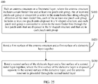
- an embodiment of this application further provides a method for producing an antenna apparatus, including: etching an antenna structure on a first metal layer, where the antenna structure includes a main feeder and at least one patch unit group, the at least one patch unit group is connected in series to the main feeder in a length direction of the main feeder, each of the at least one patch unit group includes at least two patch units disposed in a V-shaped structure, and each patch unit group is connected in series to the main feeder through the two patch units that are disposed in the V-shaped structure and that are in each patch unit group; bonding a first surface of the antenna structure and a first surface of a dielectric layer together; and bonding a second surface of the dielectric layer and a first surface of a second metal layer together, where the first surface of the dielectric layer is disposed opposite to the second surface of the dielectric layer, and the antenna structure is grounded through the second metal layer.
- each patch unit group is connected in series to the main feeder through a connection point of the two patch units that are disposed in the V-shaped structure and that are in each patch unit group.
- a polarization direction of each patch unit group is a horizontal polarization direction.
- the at least one patch unit group includes a plurality of patch unit groups.
- the plurality of patch unit groups are connected in series to two sides of the main feeder.
- the plurality of patch unit groups are alternately connected in series to the two sides of the main feeder.
- the at least one patch unit group includes a plurality of patch unit groups.
- a width of a patch unit in the plurality of patch unit groups first increases and then decreases in a first direction.
- a width of a patch unit in the plurality of patch unit groups increases in a first direction.
- a width of a patch unit in the plurality of patch unit groups decreases in a first direction.
- the antenna structure is a transmit antenna or a receive antenna.
- each patch unit group is connected in series to the main feeder through the two patch units that are disposed in the V-shaped structure and that are in each patch unit group. Because an included angle exists between the two patch units in the V-shaped structure, an aperture of the antenna structure can be reduced by adjusting the included angle. This can extend a 3 dB bandwidth of the antenna structure.
- FIG. 2 is a schematic diagram of a structure of an antenna structure 100 according to an embodiment of this application.
- the antenna structure 100 may include a main feeder 110 and at least one patch unit group.
- FIG. 2 shows a patch unit group 121 to a patch unit group 12N, where N is an integer greater than 1.
- the patch unit group 121 to the patch unit group 12N are connected in series to the main feeder 110 in a length direction of the main feeder 110.
- Each of the patch unit group 121 to the patch unit group 12N includes at least two patch units disposed in a V-shaped structure. As shown in FIG.
- the patch unit group 121 includes a patch unit 131 and a patch unit 132 that are disposed in a V-shaped structure, and each patch unit group is connected in series to the main feeder 110 through two patch units that are disposed in the V-shaped structure and that are in each patch unit group.
- FIG. 2 shows only an example in which the antenna structure 100 includes the patch unit group 121 to the patch unit group 12N.
- the antenna structure 100 may include only one patch unit group, for example, include only the patch unit group 121. This is not limited in this embodiment of this application.
- a main feeder is vertically connected to a radiation patch in series, and an aperture (that is, a size in a length direction of the radiation patch) of the antenna structure is large. Therefore, a 3 dB bandwidth of the existing antenna structure is narrow.
- dB decibel, decibel
- the 3 dB bandwidth is a corresponding frequency interval used when a maximum gain of the antenna structure decreases by 3 dB, and belongs to a general definition of a bandwidth of the antenna structure.
- an example of the 3 dB bandwidth is used to describe a technical problem and a technical effect.
- this application is not limited to using only the 3 dB bandwidth for description, and any other description used to represent the bandwidth of the antenna structure may replace the 3 dB bandwidth.
- each patch unit group is connected in series to the main feeder through the two patch units that are disposed in the V-shaped structure and that are in each patch unit group. Because an included angle exists between the two patch units in the V-shaped structure, an aperture of the antenna structure can be reduced by adjusting the included angle. This can extend a 3 dB bandwidth of the antenna structure.
- each patch unit group may be connected in series to the main feeder through the two patch units that are disposed in the V-shaped structure and that are in each patch unit group in a plurality of manners. This is not limited in this embodiment of this application.
- each patch unit group may be connected in series to the main feeder 110 through a connection point of the two patch units that are disposed in the V-shaped structure and that are in each patch unit group.
- the patch unit group 121 includes the patch unit 131 and the patch unit 132 that are disposed in a V-shaped structure, and an included angle ⁇ exists between the patch unit 131 and the patch unit 132.
- the patch unit group 121 is connected in series to the main feeder 110 through a connection point at the included angle ⁇ between the patch unit 131 and the patch unit 132.
- each patch unit group may be connected in series to the main feeder 110 through a partial region of each of the two patch units that are disposed in the V-shaped structure and that are in each patch unit group.
- the patch unit group 121 includes the patch unit 131 and the patch unit 132 that are disposed in a V-shaped structure, and an included angle ⁇ exists between the patch unit 131 and the patch unit 132.
- the patch unit group 121 is connected in series to the main feeder 110 through a partial region at one end of the patch unit 131 and one end of the patch unit 132.
- the patch unit group 121 to the patch unit group 12N may be connected in series to the main feeder 110 in a plurality of manners. This is not limited in this embodiment of this application.
- the patch unit group 121 to the patch unit group 12N may be connected in series to a same side of the main feeder 110.
- FIG. 4 shows a schematic diagram of the antenna structure 100 in which all the patch unit groups 121 to 124 are connected in series to the left side of the main feeder.
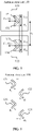
- FIG. 5 is a schematic diagram of a polarization direction of the antenna structure 100 in FIG. 4 .
- the patch unit group 121 includes the patch unit 131 and the patch unit 132.
- a polarization direction of the patch unit 131 may be decomposed into a horizontal-left F 12 and a vertical-up F 11
- a polarization direction of the patch unit 132 may be decomposed into a horizontal-left E 12 and a vertical-down E 11 .
- an interval D 1 between the patch unit group 121 and the patch unit group 122 is an integer multiple of a wavelength.
- a phase difference between the patch unit group 121 and the patch unit group 122 is 360°, that is, the polarization direction of the patch unit group 121 is same as that of the patch unit group 122. Therefore, an overall polarization direction of the patch unit group 121 and the patch unit group 122 is horizontally leftward, and a size of the patch unit group 121 and the patch unit group 122 is F 12 +E 12 +F 22 +E 22 .
- the polarization direction of the antenna structure 100 is described by using only the patch unit group 121 and the patch unit group 122 as an example.
- the polarization direction of the antenna structure 100 and an interval between patch unit groups are similar to those in FIG. 5 . To avoid repetition, details are not described herein again.
- the patch unit group 121 to the patch unit group 12N may be connected in series to two sides of the main feeder 110.
- the patch unit group 121 to the patch unit group 12N may be connected in series to the two sides of the main feeder 110 in a plurality of manners. This is not limited in this embodiment of this application.
- the patch unit group 121 to the patch unit group 12N may be alternately connected in series to two sides of the main feeder 110.
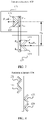
- FIG. 6 shows a schematic diagram of the antenna structure 100 in which the patch unit group 121 to the patch unit group 124 are alternately connected in series to two sides of the main feeder.
- FIG. 7 is a schematic diagram of a polarization direction of the antenna structure 100 in FIG. 6 .
- the patch unit group 121 includes the patch unit 131 and the patch unit 132.
- a polarization direction of the patch unit 131 may be decomposed into a horizontal-left F 12 and a vertical-up F 11
- a polarization direction of the patch unit 132 may be decomposed into a horizontal-left E 12 and a vertical-down E 11 .
- an interval D 2 between the patch unit group 121 and the patch unit group 122 is an odd multiple of a half wavelength.
- a phase difference between the patch unit group 121 and the patch unit group 122 is 180°, that is, the polarization direction of the patch unit group 121 is opposite to that of the patch unit group 122. Therefore, an overall polarization direction of the patch unit group 121 and the patch unit group 122 is horizontally leftward (or rightward), and a size of the patch unit group 121 and the patch unit group 122 is F 12 +E 12 +F 22 +E 22 .
- the polarization direction of the antenna structure 100 is described by using only the patch unit group 121 and the patch unit group 122 as an example.
- the polarization direction of the antenna structure 100 and an interval between patch unit groups are similar to those in FIG. 7 . To avoid repetition, details are not described herein again.
- some of the patch unit groups 121 to 12N may be sequentially connected in series to one side of the main feeder 110, and the rest of patch unit groups may be sequentially connected in series to the other side of the main feeder 110.
- the antenna structure 100 includes four patch unit groups.
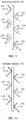
- FIG. 8 is a schematic diagram of the antenna structure 100 in which the patch unit group 121 and the patch unit group 122 are connected in series to the left side of the main feeder, and the patch unit group 123 and the patch unit group 124 are connected in series to the right side of the main feeder.
- an interval between patch unit groups when the patch unit group 121 to the patch unit group 12N are connected in series to two sides of the main feeder 110 is shorter than an interval between patch unit groups when the patch unit group 121 to the patch unit group 12N are connected in series to the same side of the main feeder 110. Therefore, the patch unit group 121 to the patch unit group 12N are connected in series to two sides of the main feeder, so that the size of the main feeder can be reduced.
- an interval between the patch unit groups when the patch unit group 121 to the patch unit group 12N are alternately connected in series to two sides of the main feeder 110 is shorter than an interval between the patch unit groups when some of the patch unit group 121 to the patch unit group 12N are first connected in series to one side of the main feeder 110, and the other of the patch unit group 121 to the patch unit group 12N are then connected in series to the other side of the main feeder 110, and an interval between the patch unit groups when the patch unit group 121 to the patch unit group 12N are connected in series to the same side of the main feeder 110. Therefore, the patch unit groups 121 to 12N are alternately connected in series to two sides of the main feeder 110, so that the size of the main feeder can be reduced.
- widths of the patch units in each patch unit group may be set to different values. This is not limited in this embodiment of this application.
- widths of the patch units in the patch unit group 121 to the patch unit group 12N first increase and then decrease in a first direction.
- the first direction may be a length direction of the main feeder.
- the antenna structure 100 includes the patch unit group 121 to a patch unit group 126, widths of patch units in the patch unit group 121 to the patch unit group 126 are sequentially d 1 to d 6 , and d 1 ⁇ d 2 ⁇ d 3 ⁇ d 4 >d 5 >d 6 .
- widths of patch units in the patch unit group 121 to the patch unit group 12N increase or decrease in the first direction.
- the antenna structure 100 includes the patch unit group 121 to the patch unit group 126, widths of patch units in the patch unit group 121 to the patch unit group 126 are sequentially d 1 to d 6 , and d 1 ⁇ d 2 ⁇ d 3 ⁇ d 4 ⁇ d 5 ⁇ d 6 .
- widths of the patch units in the patch unit group 121 to the patch unit group 12N are the same.
- widths of patch units in different patch unit groups may be the same or may be different. This is not limited in this embodiment of this application.
- widths of the patch units in the different patch unit groups are the same includes being exactly the same and being approximately the same, where being approximately the same means that a difference between the widths of the patch units in the different patch unit groups is within a specific error range.
- the widths of the patch units in the patch unit group are designed, so that requirements for different electromagnetic wave radiation shapes can be met. For example, when the width of the patch unit designed in the foregoing first possible implementation is used, because energy is concentrated in a middle segment of the main feeder, a low sidelobe can be implemented. This reduces a false alarm probability.
- an included angle between two patch units that are disposed in a V shape and that are in each patch unit group and an included angle between each patch unit group and the main feeder may be of different sizes. This is not limited in this embodiment of this application.
- the included angle between the two patch units in each patch unit group may be 90°.
- the included angle between each patch unit group and the main feeder may be 45°.
- the included angle between the two patch units that are disposed in the V-shaped structure and that are in each patch unit is set, so that different aperture requirements of the antenna structure can be met, a horizontal beam width of an antenna can be further broadened, and a low sidelobe requirement of a vertical plane can be further implemented.
- lengths of the patch units in each patch unit group may be set to be of different sizes. This is not limited in this embodiment of this application.
- lengths of the patch units in the patch unit group 121 to the patch unit group 12N first increase and then decrease in a first direction.
- the first direction may be a length direction of the main feeder.
- the antenna structure 100 includes the patch unit group 121 to the patch unit group 126, lengths of patch units in the patch unit group 121 to the patch unit group 126 are sequentially s 1 to s 6 , and s 1 ⁇ s 2 ⁇ s 3 ⁇ s 4 >s 5 >s 6 .
- lengths of the patch units in the patch unit group 121 to the patch unit group 12N increase or decrease in a first direction.
- the antenna structure 100 includes the patch unit group 121 to the patch unit group 126, lengths of the patch units in the patch unit group 121 to the patch unit group 126 are sequentially s 1 to s 6 , and s 1 ⁇ s 2 ⁇ s 3 ⁇ s 4 ⁇ s 5 ⁇ s 6 .
- lengths of the patch units in the patch unit group 121 to the patch unit group 12N are the same.
- lengths of patch units in different patch unit groups may be the same or may be different. This is not limited in this embodiment of this application.
- the lengths of the patch units in the different patch unit groups are the same includes being exactly the same and being approximately the same, where being approximately the same means that a difference between the lengths of the patch units in the different patch unit groups is within a specific error range.
- a size of a patch unit in each patch unit group includes a length and a width.
- sizes of patch units in different patch unit groups may be the same or may be different. This is not limited in this embodiment of this application.
- the sizes of the patch units in the different patch unit groups are the same includes being exactly the same and being approximately the same, where being approximately the same means that a difference between the sizes of the patch units in the different patch unit groups is within a specific error range.
- each patch unit group includes two patch units disposed in a V-shaped structure may be understood as follows: The two patch units are disposed in a V-shaped structure, or the two patch units are disposed in a similar V-shaped structure. This is not limited in this embodiment of this application.
- each patch unit group may be of a C-shaped structure.
- the two patch units included in each patch unit group may be of an L-shaped structure.
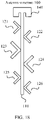
- FIG. 16 is still another schematic diagram of a structure of the antenna structure 100.
- the antenna structure 100 includes the patch unit group 121 to the patch unit group 124.
- Each patch unit group includes two patch units disposed in a C-shaped structure.
- the patch units in each patch unit group may have a plurality of different shapes. This is not limited in this embodiment of this application.
- the patch unit in each patch unit group may be rectangular, as shown in FIG. 1 to FIG. 15 .
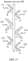
- the patch unit in each patch unit group may be in the shape of a polygon, for example, a parallelogram, as shown in FIG. 17 .
- shapes of the patch units in each patch unit group may be the same or may be different. This is not limited in this embodiment of this application.
- the antenna structure may operate in a standing wave mode or a traveling wave mode. This is not limited in this embodiment of this application.
- a standing wave and a traveling wave are phenomena that appear in a wave propagation process.
- traveling wave A wave is transmitted from a wave source.
- an equal amplitude high-frequency alternating current power supply is used to drive a pair of infinitely long parallel wires, there is a high-frequency alternating voltage and a high-frequency alternating current that are synchronized with the power supply in a conducting wire near a power supply end.
- a current flowing through is a high-frequency alternating current of a same amplitude, but a time phase of the current flowing through each section is different.
- a current at each point at a same moment is in sinusoidal distribution with a distance from the power supply end. It seems that a sinusoidal current wave continuously flows from the infinite end to the power supply along a conducting wire, and then from the power supply to the infinite end along another conducting wire. This flow mode of the current wave is called a traveling wave.
- a maximum beam direction angle of the antenna structure changes with a frequency. This phenomenon is referred to as frequency scanning.
- a frequency scanning range of the antenna structure can be reduced.
- Standing wave A wave is reflected back and forth in space. The reflected wave interferes with a subsequent wave to form a stable interference field. An amplitude of each part is stable. A location where the amplitude is zero is called a wave node, and a location where the amplitude is the largest is called a wave abdomen.
- This disturbance can also be considered as energy transmitted from the power supply because the energy cannot be transmitted continuously and there is no place to use up the energy. Therefore, the energy can only be reflected back.
- a voltage and a current at each point have a same phase and each point has its own fixed amplitude. It seems that the voltage wave and current wave do not move along the conducting wire. This flow mode of the current wave is called a standing wave.
- load matching means a maximum output power from a perspective of power, that is, in a power supply circuit, load impedance is equal to a conjugate value of impedance in the power supply (resistances are equal, reactances are equal, and symbols are opposite).
- the purpose of matching is to obtain the maximum output power. From a perspective of a transmission line, it means lossless transmission, that is, on the transmission line, load impedance is equal to characteristic impedance of the transmission line, which is called "matching".
- the purpose of matching is to eliminate a reflection caused by load, avoid a standing wave, and enable the load to obtain maximum power.
- a signal source is a transmitter
- load is an antenna feeder subsystem
- the antenna feeder subsystem includes auxiliary devices such as an antenna, a feeder, a radio frequency connector, and a lightning arrester. Otherwise, if the load does not match the signal source, some signals will be reflected back to the signal source, which is undesirable. In this case, a forward wave and a reverse wave are generated, and the two signals are combined to form a standing wave.
- a first end of the antenna structure when the antenna structure operates in the standing wave mode, a first end of the antenna structure does not include a load matching unit.
- a first end of the antenna structure does not include a load matching unit may be understood as that the first end of the antenna structure is open-circuited.
- all the antenna structures 100 shown in FIG. 1 to FIG. 17 are antenna structures working in the standing wave mode.
- a second end of the antenna structure when the antenna structure operates in the traveling wave mode, a second end of the antenna structure further includes a load matching unit.
- the load matching unit is configured to consume energy that is not consumed totally by the at least one patch unit group.
- the load matching unit may be connected to the first end of the main feeder in a plurality of manners. This is not limited in this embodiment of this application.
- the load matching unit is in a same length direction as the main feeder.
- FIG. 18 is still another schematic diagram of a structure of the antenna structure 100 according to an embodiment of this application.
- a first end of the antenna structure includes a load matching unit 140, and a length direction of the load matching unit 140 is the same as a length direction of the main feeder 110.
- the load matching unit is connected to the main feeder by bending.
- FIG. 19 is still another schematic diagram of a structure of the antenna structure 100 according to an embodiment of this application.
- a first end of the antenna structure includes a load matching unit 140, and the load matching unit 140 connected to the main feeder 110 by bending, that is, an included angle exists between the load matching unit 140 and the main feeder 110.
- the antenna structure may be a receive antenna or a transmit antenna. This is not limited in this embodiment of this application.
- a left sidelobe level of a beam can be -21.2 dB
- a right sidelobe level of a beam can be -17.8 dB
- a 3 dB beam width can be 97°.
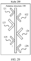
- FIG. 20 is a schematic diagram of a structure of a radar 200 according to an embodiment of this application.
- the radar 300 may include the antenna structure 100 shown in FIG. 2 to FIG. 19 .
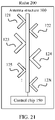
- the radar 200 further includes a control chip 150.
- the control chip 150 is connected to a second end of the antenna structure, and the control chip 150 is configured to control the antenna structure to transmit or receive a signal.
- control chip 150 may be connected to the second end of the antenna structure through a first microstrip line.
- the radar 200 further includes an impedance matching unit 160.
- the impedance matching unit 160 is configured to match impedance of the second end with impedance of the control chip 150, and the control chip 150 is connected to the second end through the impedance matching unit.
- the impedance matching unit may be a second microstrip line.
- the impedance of the second end of the antenna structure can match the impedance of the control chip by adjusting impedance of the second microstrip line.
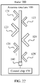
- the radar 200 further includes a printed circuit board 170.
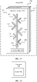
- the printed circuit board 170 includes the antenna structure 100 (shown as in FIG. 23 ), a dielectric layer 171 (shown as in FIG. 23 ), and a metal layer 172 (shown as in FIG. 23 ) that are sequentially disposed in a stacked manner.
- the antenna structure is grounded through the metal layer.
- FIG. 24 shows a terminal 300 according to an embodiment of this application.
- the terminal 300 includes the radar 200 described in FIG. 20 to FIG. 23 .
- the terminal in this embodiment of this application may have a capability of implementing a communication function and/or a detection function through a radar. This is not limited in this embodiment of this application.
- the terminal may be a vehicle, an unmanned aerial vehicle, an unmanned transport vehicle, a robot, or the like in self-driving or intelligent driving.
- the terminal may be a mobile phone (mobile phone), a tablet computer (pad), a computer with a wireless transceiver function, a virtual reality (virtual reality, VR) terminal, or an augmented reality (augmented reality, AR) terminal, a wireless terminal in industrial control (industrial control), a wireless terminal in self-driving (self-driving), a wireless terminal in telemedicine (remote medical), a wireless terminal in a smart grid (smart grid), a wireless terminal in transportation safety (transportation safety), a wireless terminal in a smart city (smart city), a wireless terminal in a smart home (smart home), and the like.
- FIG. 25 shows a method 400 for producing an antenna apparatus according to an embodiment of this application.
- the method 400 includes the following steps S410 to S430.
- each of the at least one patch unit group includes at least two patch units disposed in a V-shaped structure, and each patch unit group is connected in series to the main feeder through the two patch units that are in the V-shaped structure and that are on each patch unit group.
- each patch unit group is connected in series to the main feeder through a connection point of the two patch units that are disposed in the V-shaped structure and that are in each patch unit group.
- a polarization direction of each patch unit group is a horizontal polarization direction.
- the at least one patch unit group includes a plurality of patch unit groups, and the plurality of patch unit groups are connected in series to two sides of the main feeder.
- the plurality of patch unit groups are alternately connected in series to two sides of the main feeder.
- the at least one patch unit group includes a plurality of patch unit groups.
- a width of a patch unit in the plurality of patch unit groups first increases and then decreases in a first direction.
- a width of a patch unit in the plurality of patch unit groups increases in a first direction.
- a width of a patch unit in the plurality of patch unit groups decreases in a first direction.
- each patch unit group is connected in series to the main feeder through the two patch units that are disposed in the V-shaped structure and that are in each patch unit group. Because an included angle exists between the two patch units in the V-shaped structure, an aperture of the antenna structure can be reduced by adjusting the included angle. This can extend a 3 dB bandwidth of the antenna structure.
- the disclosed system, apparatus and method may be implemented in other manners.
- the described apparatus embodiment is merely an example.
- division into the units is merely logical function division and may be other division in an actual implementation.
- a plurality of units or components may be combined or integrated into another system, or some features may be ignored or not performed.
- the displayed or discussed mutual couplings or direct couplings or communication connections may be implemented through some interfaces.
- the indirect couplings or communication connections between the apparatuses or units may be implemented in electrical, mechanical, or other forms.
- the units described as separate parts may or may not be physically separate, and parts displayed as units may or may not be physical units, may be located in one location, or may be distributed on a plurality of network units. Some or all of the units may be selected based on an actual requirement to achieve the objectives of the solutions in embodiments.
- functional units in embodiments of this application may be integrated into one processing unit, or each of the units may exist alone physically, or two or more units are integrated into one unit.
- the functions When the functions are implemented in the form of a software functional unit and sold or used as an independent product, the functions may be stored in a computer-readable storage medium. Based on such an understanding, the technical solutions of this application essentially, or the part contributing to the conventional technology, or some of the technical solutions may be implemented in a form of a software product.
- the computer software product is stored in a storage medium, and includes several instructions for instructing a computer device (which may be a personal computer, a server, a network device, or the like) to perform all or some of the steps of the methods described in embodiments of this application.
- the foregoing storage medium includes any medium that can store program code, for example, a USB flash drive, a removable hard disk, a read-only memory (read-only memory, ROM), a random access memory (random access memory, RAM), a magnetic disk, or an optical disc.
- a USB flash drive for example, a USB flash drive, a removable hard disk, a read-only memory (read-only memory, ROM), a random access memory (random access memory, RAM), a magnetic disk, or an optical disc.
Landscapes
- Engineering & Computer Science (AREA)
- Radar, Positioning & Navigation (AREA)
- Remote Sensing (AREA)
- Computer Security & Cryptography (AREA)
- Computer Networks & Wireless Communication (AREA)
- Physics & Mathematics (AREA)
- General Physics & Mathematics (AREA)
- Waveguide Aerials (AREA)
- Variable-Direction Aerials And Aerial Arrays (AREA)
- Details Of Aerials (AREA)
- Radar Systems Or Details Thereof (AREA)
Abstract
Description
- This application relates to the field of sensor technologies, and more specifically, to an antenna structure, a radar, and a terminal in the field of sensor technologies.
- With development of society and progress of science and technology, intelligent vehicles gradually enter people's daily lives. A sensor plays a very important role in unmanned driving and intelligent driving of an intelligent vehicle. The sensor may be a millimeter-wave radar, a laser radar, an ultrasonic radar, a camera, or the like. For example, as a key sensor of the unmanned driving technology, a 77 GHz millimeter-wave radar has features such as a short wavelength and a small device size. The 77 GHz millimeter-wave radar has irreplaceable advantages in terms of detection precision, detection distance, and device integration.
- From perspectives of a detection scenario and an implementation function of the radar, an antenna used by the radar is required to have a wide 3 dB beam bandwidth and a low sidelobe. The wide 3 dB beam bandwidth can ensure a large detection angle range in a horizontal direction, and the low sidelobe can reduce clutter energy reflected by the ground in a vertical direction. Consequently, a false alarm probability is reduced.
-
FIG. 1 is a schematic diagram of a structure of an existing antenna structure. The existing antenna structure uses a series-feed mode, that is, a plurality of radiation patches that are vertically connected to a feeder are simultaneously excited by using one feeder. Widths of the plurality of radiation patches first gradually increase and then gradually decrease in a length direction of the feeder, that is, energy radiated by the antenna structure is concentrated in a middle area close to a length of the feeder, so that low sidelobe weighting can be implemented. This avoids radar false alarm. - However, the existing antenna structure shown in
FIG. 1 may implement a low sidelobe level, but has a small 3 dB beam width. This leads to a small detection angle range in the horizontal direction. - Embodiments of this application provide an antenna structure, a radar, and a terminal, to extend a 3 dB bandwidth of the antenna structure.
- According to a first aspect, an embodiment of this application provides an antenna structure. The antenna structure includes a main feeder and at least one patch unit group. The at least one patch unit group is connected in series to the main feeder in a length direction of the main feeder. Each of the at least one patch unit group includes at least two patch units disposed in a V-shaped structure. Each patch unit group is connected in series to the main feeder through the two patch units that are disposed in the V-shaped structure and that are in each patch unit group.
- According to the antenna structure provided in this embodiment of this application, each patch unit group is connected in series to the main feeder through the two patch units that are disposed in the V-shaped structure and that are in each patch unit group. Because an included angle exists between the two patch units in the V-shaped structure, an aperture of the antenna structure can be reduced by adjusting the included angle. This can extend a 3 dB bandwidth of the antenna structure.
- The following uses an example in which the at least one patch unit group includes a plurality of patch unit groups for description.
- Optionally, each patch unit group may be connected in series to the main feeder through the two patch units that are disposed in the V-shaped structure and that are in each patch unit group in a plurality of manners. This is not limited in this embodiment of this application.
- In a possible implementation, each patch unit group is connected in series to the main feeder through a connection point of the two patch units that are disposed in the V-shaped structure and that are in each patch unit group.
- In another possible implementation, each patch unit group may be connected in series to the main feeder through a partial region of each of the two patch units that are disposed in the V-shaped structure and that are in each patch unit group.
- Optionally, the plurality of patch unit groups may be connected in series to the main feeder in a plurality of manners. This is not limited in this embodiment of this application.
- In a first possible implementation, the plurality of patch unit groups may be connected in series to a same side of the main feeder.
- In a second possible implementation, the plurality of patch unit groups may be connected in series to two sides of the main feeder.
- According to the antenna structure provided in this embodiment of this application, compared with a case in which the plurality of patch units are connected in series to the same side of the main feeder, a case in which the plurality of patch units are connected in series to the two sides of the main feeder can increase a horizontal radiation range.
- Optionally, the plurality of patch unit groups may be connected in series to the two sides of the main feeder in a plurality of manners. This is not limited in this embodiment of this application.
- In a possible implementation, the plurality of patch unit groups are alternately connected in series to two sides of the main feeder.
- In another possible implementation, some of the plurality of patch unit groups may be sequentially connected in series to one side of the main feeder, and the rest of patch unit groups may be sequentially connected in series to the other side of the main feeder.
- According to the antenna structure provided in this embodiment of this application, an interval between the patch unit groups when the plurality of patch unit groups are connected in series to the two sides of the main feeder is shorter than an interval between the patch unit groups when the plurality of patch unit groups are connected in series to the same side of the main feeder. The plurality of patch unit groups are connected in series to two sides of the main feeder, so that a size of the main feeder can be reduced.
- In addition, an interval between the patch unit groups when the plurality of patch unit groups are alternately connected in series to two sides of the main feeder is shorter than an interval between the patch unit groups when some of the plurality of patch unit groups are first connected in series to one side of the main feeder, and the other of patch unit groups are then connected in series to the other side of the main feeder, and an interval between the patch unit groups when the plurality of patch unit groups are connected in series to the same side of the main feeder. Therefore, the plurality of patch unit groups are alternately connected in series to two sides of the main feeder, so that a size of the main feeder can be reduced.
- Optionally, widths of the patch units in each patch unit group may be set to different values. This is not limited in this embodiment of this application.
- In a first possible implementation, a width of a patch unit in the plurality of patch unit groups first increases and then decreases in a first direction.
- In a second possible implementation, a width of a patch unit in the plurality of patch unit groups increases or decreases in a first direction.
- In a third possible implementation, a width of a patch unit in the plurality of patch unit groups is the same.
- Optionally, widths of patch units in different patch unit groups may be the same or may be different. This is not limited in this embodiment of this application.
- It should be noted that, in this embodiment of this application, that the widths of the patch units in the different patch unit groups are the same includes being exactly the same and being approximately the same, where being approximately the same means that a difference between the widths of the patch units in the different patch unit groups is within a specific error range.
- According to the antenna structure provided in this embodiment of this application, the widths of the patch units in the patch unit group are designed, so that requirements for different electromagnetic wave radiation shapes can be met. For example, when the width of the patch unit designed in the foregoing first possible implementation is used, because energy is concentrated in a middle segment of the main feeder, a low sidelobe can be implemented. This reduces a false alarm probability.
- Optionally, an included angle between two patch units that are disposed in a V shape and that are in each patch unit group and an included angle between each patch unit group and the main feeder may be of different sizes. This is not limited in this embodiment of this application.
- In a possible implementation, the included angle between the two patch units in each patch unit group may be 90°.
- In another possible implementation, the included angle between each patch unit group and the main feeder may be 45°.
- According to the antenna structure provided in this embodiment of this application, the included angle between the two patch units that are disposed in the V-shaped structure and that are in each patch unit is set, so that different aperture requirements of the antenna structure can be met, a horizontal beam width of an antenna can be further broadened, and a low sidelobe requirement of a vertical plane can be further implemented.
- Optionally, lengths of the patch units in each patch unit group may be set to be of different sizes. This is not limited in this embodiment of this application.
- In a first possible implementation, lengths of the patch units in the plurality of patch unit groups first increase and then decrease in a first direction.
- In a second possible implementation, lengths of the patch units in the plurality of patch unit groups increase or decrease in a first direction.
- In a third possible implementation, lengths of the patch units in the plurality of patch unit groups are the same.
- Optionally, lengths of the patch units in different patch unit groups may be the same or may be different. This is not limited in this embodiment of this application.
- It should be noted that, in this embodiment of this application, that the lengths of the patch units in the different patch unit groups are the same includes being exactly the same and being approximately the same, where being approximately the same means that a difference between the lengths of the patch units in the different patch unit groups is within a specific error range.
- It should be noted that a size of a patch unit in each patch unit group includes a length and a width.
- Optionally, sizes of patch units in different patch unit groups may be the same or may be different. This is not limited in this embodiment of this application.
- It should be noted that, in this embodiment of this application, that the sizes of the patch units in the different patch unit groups are the same includes being exactly the same and being approximately the same, where being approximately the same means that a difference between the sizes of the patch units in the different patch unit groups is within a specific error range.
- It should be noted that, that each patch unit group includes two patch units disposed in a V-shaped structure may be understood as follows: The two patch units are disposed in a V-shaped structure, or the two patch units are disposed in a similar V-shaped structure. This is not limited in this embodiment of this application.
- In a possible implementation, the two patch units included in each patch unit group may be of a C-shaped structure.
- In another possible implementation, the two patch units included in each patch unit group may be of an L-shaped structure.
- In a possible implementation, the patch unit in each patch unit group may be rectangular.
- In another possible implementation, the patch unit in each patch unit group may be in the shape of a polygon, for example, a parallelogram.
- Optionally, shapes of the patch units in each patch unit group may be the same or may be different. This is not limited in this embodiment of this application.
- Optionally, the antenna structure may operate in a standing wave mode or a traveling wave mode. This is not limited in this embodiment of this application.
- In a first possible implementation, when the antenna structure operates in the standing wave mode, a first end of the antenna structure does not include a load matching unit.
- It should be noted that, that a first end of the antenna structure does not include a load matching unit may be understood as that the first end of the antenna structure is open-circuited.
- In a second possible implementation, when the antenna structure operates in the traveling wave mode, a second end of the antenna structure further includes a load matching unit. The load matching unit is configured to consume energy that is not consumed totally by the at least one patch unit group.
- Optionally, the load matching unit may be connected to the first end of the main feeder in a plurality of manners. This is not limited in this embodiment of this application.
- In a first possible implementation, the load matching unit is in a same length direction as the main feeder.
- In a second possible implementation, the load matching unit is connected to the main feeder by bending.
- According to the antenna structure provided in this embodiment of this application, flexibility of accessing the load matching unit can be improved by changing a bending angle between the load matching unit and the main feeder.
- According to a second aspect, an embodiment of this application further provides a radar. The radar includes the antenna structure according to any one of the first aspect or the possible implementations of the first aspect.
- In a possible implementation, the radar further includes a control chip. The control chip is connected to a second end of the antenna structure. The control chip is configured to control the antenna structure to transmit or receive a signal.
- It should be noted that the control chip may be connected to the second end of the antenna structure through a first microstrip line.
- In a possible implementation, the radar further includes an impedance matching unit. The impedance matching unit is configured to match impedance of the second end with impedance of the control chip, and the control chip is connected to the second end through the impedance matching unit.
- It should be noted that the impedance matching unit may be a second microstrip line.
- That is, the impedance of the second end of the antenna structure can match the impedance of the control chip by adjusting impedance of the second microstrip line.
- In a possible implementation, the radar further includes a printed circuit board. The printed circuit board includes the antenna structure, a dielectric layer, and a metal layer that are sequentially disposed in a stacked manner. The antenna structure is grounded through the metal layer.
- According to a third aspect, an embodiment of this application further provides a terminal. The terminal includes the radar according to the second aspect or the possible implementations of the second aspect.
- Optionally, the terminal in this embodiment of this application may have a capability of implementing a communication function and/or a detection function through a radar. This is not limited in this embodiment of this application.
- In a possible implementation, the terminal may be a vehicle, an unmanned aerial vehicle, an unmanned transport vehicle, a robot, or the like in self-driving or intelligent driving.
- In another possible implementation, the terminal may be a mobile phone, a tablet computer, a computer with a wireless transceiver function, a virtual reality terminal, an augmented reality terminal, a wireless terminal in industrial control, a wireless terminal in unmanned driving, a wireless terminal in telemedicine, a wireless terminal in a smart grid, a wireless terminal in transportation safety, a wireless terminal in a smart city, a wireless terminal in a smart home, or the like.
- According to a fourth aspect, an embodiment of this application further provides a method for producing an antenna apparatus, including: etching an antenna structure on a first metal layer, where the antenna structure includes a main feeder and at least one patch unit group, the at least one patch unit group is connected in series to the main feeder in a length direction of the main feeder, each of the at least one patch unit group includes at least two patch units disposed in a V-shaped structure, and each patch unit group is connected in series to the main feeder through the two patch units that are disposed in the V-shaped structure and that are in each patch unit group; bonding a first surface of the antenna structure and a first surface of a dielectric layer together; and bonding a second surface of the dielectric layer and a first surface of a second metal layer together, where the first surface of the dielectric layer is disposed opposite to the second surface of the dielectric layer, and the antenna structure is grounded through the second metal layer.
- In a possible implementation, each patch unit group is connected in series to the main feeder through a connection point of the two patch units that are disposed in the V-shaped structure and that are in each patch unit group.
- In a possible implementation, a polarization direction of each patch unit group is a horizontal polarization direction.
- In a possible implementation, the at least one patch unit group includes a plurality of patch unit groups. The plurality of patch unit groups are connected in series to two sides of the main feeder.
- In a possible implementation, the plurality of patch unit groups are alternately connected in series to the two sides of the main feeder.
- In a possible implementation, the at least one patch unit group includes a plurality of patch unit groups. A width of a patch unit in the plurality of patch unit groups first increases and then decreases in a first direction. Alternatively, a width of a patch unit in the plurality of patch unit groups increases in a first direction. Alternatively, a width of a patch unit in the plurality of patch unit groups decreases in a first direction.
- In a possible implementation, the antenna structure is a transmit antenna or a receive antenna.
- According to the antenna structure provided in this embodiment of this application, each patch unit group is connected in series to the main feeder through the two patch units that are disposed in the V-shaped structure and that are in each patch unit group. Because an included angle exists between the two patch units in the V-shaped structure, an aperture of the antenna structure can be reduced by adjusting the included angle. This can extend a 3 dB bandwidth of the antenna structure.
-
-
FIG. 1 is a schematic diagram of a structure of an antenna structure in the conventional technology; -
FIG. 2 is a schematic diagram of a structure of anantenna structure 100 according to an embodiment of this application; -
FIG. 3 is another schematic diagram of a structure of anantenna structure 100 according to an embodiment of this application; -
FIG. 4 is still another schematic diagram of a structure of anantenna structure 100 according to an embodiment of this application; -
FIG. 5 is still another schematic diagram of a structure of anantenna structure 100 according to an embodiment of this application; -
FIG. 6 is still another schematic diagram of a structure of anantenna structure 100 according to an embodiment of this application; -
FIG. 7 is still another schematic diagram of a structure of anantenna structure 100 according to an embodiment of this application; -
FIG. 8 is still another schematic diagram of a structure of anantenna structure 100 according to an embodiment of this application; -
FIG. 9 is still another schematic diagram of a structure of anantenna structure 100 according to an embodiment of this application; -
FIG. 10 is still another schematic diagram of a structure of anantenna structure 100 according to an embodiment of this application; -
FIG. 11 is still another schematic diagram of a structure of anantenna structure 100 according to an embodiment of this application; -
FIG. 12 is still another schematic diagram of a structure of anantenna structure 100 according to an embodiment of this application; -
FIG. 13 is still another schematic diagram of a structure of anantenna structure 100 according to an embodiment of this application; -
FIG. 14 is still another schematic diagram of a structure of anantenna structure 100 according to an embodiment of this application; -
FIG. 15 is still another schematic diagram of a structure of anantenna structure 100 according to an embodiment of this application; -
FIG. 16 is still another schematic diagram of a structure of anantenna structure 100 according to an embodiment of this application; -
FIG. 17 is still another schematic diagram of a structure of anantenna structure 100 according to an embodiment of this application; -
FIG. 18 is still another schematic diagram of a structure of anantenna structure 100 according to an embodiment of this application; -
FIG. 19 is still another schematic diagram of a structure of anantenna structure 100 according to an embodiment of this application; -
FIG. 20 is a schematic diagram of a structure of aradar 200 according to an embodiment of this application; -
FIG. 21 is another schematic diagram of a structure of aradar 200 according to an embodiment of this application; -
FIG. 22 is still another schematic diagram of a structure of aradar 200 according to an embodiment of this application; -
FIG. 23 is still yet another schematic diagram of a structure of aradar 200 according to an embodiment of this application; -
FIG. 24 is a schematic diagram of a structure of a terminal 300 according to an embodiment of this application; and -
FIG. 25 is a schematic flowchart of amethod 400 for producing an antenna apparatus according to an embodiment of this application. - The following describes technical solutions of this application with reference to accompanying drawings.
-
FIG. 2 is a schematic diagram of a structure of anantenna structure 100 according to an embodiment of this application. Theantenna structure 100 may include amain feeder 110 and at least one patch unit group.FIG. 2 shows apatch unit group 121 to apatch unit group 12N, where N is an integer greater than 1. Thepatch unit group 121 to thepatch unit group 12N are connected in series to themain feeder 110 in a length direction of themain feeder 110. Each of thepatch unit group 121 to thepatch unit group 12N includes at least two patch units disposed in a V-shaped structure. As shown inFIG. 2 , thepatch unit group 121 includes apatch unit 131 and apatch unit 132 that are disposed in a V-shaped structure, and each patch unit group is connected in series to themain feeder 110 through two patch units that are disposed in the V-shaped structure and that are in each patch unit group. - It should be noted that
FIG. 2 shows only an example in which theantenna structure 100 includes thepatch unit group 121 to thepatch unit group 12N. Theantenna structure 100 may include only one patch unit group, for example, include only thepatch unit group 121. This is not limited in this embodiment of this application. - In an existing antenna structure, a main feeder is vertically connected to a radiation patch in series, and an aperture (that is, a size in a length direction of the radiation patch) of the antenna structure is large. Therefore, a 3 dB bandwidth of the existing antenna structure is narrow.
- It should be noted that dB (decibel, decibel) in this embodiment of this application is a unit of a power gain, and the 3 dB bandwidth is a corresponding frequency interval used when a maximum gain of the antenna structure decreases by 3 dB, and belongs to a general definition of a bandwidth of the antenna structure. In this application, an example of the 3 dB bandwidth is used to describe a technical problem and a technical effect. However, this application is not limited to using only the 3 dB bandwidth for description, and any other description used to represent the bandwidth of the antenna structure may replace the 3 dB bandwidth.
- According to the antenna structure provided in this embodiment of this application, each patch unit group is connected in series to the main feeder through the two patch units that are disposed in the V-shaped structure and that are in each patch unit group. Because an included angle exists between the two patch units in the V-shaped structure, an aperture of the antenna structure can be reduced by adjusting the included angle. This can extend a 3 dB bandwidth of the antenna structure.
- Optionally, each patch unit group may be connected in series to the main feeder through the two patch units that are disposed in the V-shaped structure and that are in each patch unit group in a plurality of manners. This is not limited in this embodiment of this application.
- In a possible implementation, each patch unit group may be connected in series to the
main feeder 110 through a connection point of the two patch units that are disposed in the V-shaped structure and that are in each patch unit group. - For example, in
FIG. 2 , thepatch unit group 121 includes thepatch unit 131 and thepatch unit 132 that are disposed in a V-shaped structure, and an included angle α exists between thepatch unit 131 and thepatch unit 132. Thepatch unit group 121 is connected in series to themain feeder 110 through a connection point at the included angle α between thepatch unit 131 and thepatch unit 132. - In another possible implementation, each patch unit group may be connected in series to the
main feeder 110 through a partial region of each of the two patch units that are disposed in the V-shaped structure and that are in each patch unit group. - For example, in
FIG. 3 , thepatch unit group 121 includes thepatch unit 131 and thepatch unit 132 that are disposed in a V-shaped structure, and an included angle α exists between thepatch unit 131 and thepatch unit 132. Thepatch unit group 121 is connected in series to themain feeder 110 through a partial region at one end of thepatch unit 131 and one end of thepatch unit 132. - Optionally, the
patch unit group 121 to thepatch unit group 12N may be connected in series to themain feeder 110 in a plurality of manners. This is not limited in this embodiment of this application. - In a first possible implementation, the
patch unit group 121 to thepatch unit group 12N may be connected in series to a same side of themain feeder 110. - For example, using an example in which the
antenna structure 100 includes four patch unit groups,FIG. 4 shows a schematic diagram of theantenna structure 100 in which all thepatch unit groups 121 to 124 are connected in series to the left side of the main feeder. - It should be noted that
FIG. 5 is a schematic diagram of a polarization direction of theantenna structure 100 inFIG. 4 . As shown inFIG. 5 , thepatch unit group 121 includes thepatch unit 131 and thepatch unit 132. A polarization direction of thepatch unit 131 may be decomposed into a horizontal-left F12 and a vertical-up F11, and a polarization direction of thepatch unit 132 may be decomposed into a horizontal-left E12 and a vertical-down E11. When both an included angle between thepatch unit 131 and the horizontal direction and an included angle between thepatch unit 132 and the horizontal direction are 45°, F11 and E11 of thepatch unit 121 counteract each other in the vertical direction, and F12 and E12 are superposed in the horizontal direction. Therefore, the polarization direction of thepatch unit group 121 is horizontally leftward, and a size of thepatch unit group 121 is F12+E12. Similarly, the polarization direction of thepatch unit group 122 is horizontally leftward, and a size of thepatch unit group 122 is F22+E22. - In addition, in
FIG. 5 , an interval D1 between thepatch unit group 121 and thepatch unit group 122 is an integer multiple of a wavelength. In this way, a phase difference between thepatch unit group 121 and thepatch unit group 122 is 360°, that is, the polarization direction of thepatch unit group 121 is same as that of thepatch unit group 122. Therefore, an overall polarization direction of thepatch unit group 121 and thepatch unit group 122 is horizontally leftward, and a size of thepatch unit group 121 and thepatch unit group 122 is F12+E12+F22+E22. - It should be noted that, in
FIG. 5 , the polarization direction of theantenna structure 100 is described by using only thepatch unit group 121 and thepatch unit group 122 as an example. When a plurality of patch unit groups included in theantenna structure 100 are connected in series to the left side of the main feeder, the polarization direction of theantenna structure 100 and an interval between patch unit groups are similar to those inFIG. 5 . To avoid repetition, details are not described herein again. - In a second possible implementation, the
patch unit group 121 to thepatch unit group 12N may be connected in series to two sides of themain feeder 110. - Optionally, the
patch unit group 121 to thepatch unit group 12N may be connected in series to the two sides of themain feeder 110 in a plurality of manners. This is not limited in this embodiment of this application. - In a possible implementation, the
patch unit group 121 to thepatch unit group 12N may be alternately connected in series to two sides of themain feeder 110. - For example, using an example in which the
antenna structure 100 includes four patch unit groups,FIG. 6 shows a schematic diagram of theantenna structure 100 in which thepatch unit group 121 to thepatch unit group 124 are alternately connected in series to two sides of the main feeder. - It should be noted that
FIG. 7 is a schematic diagram of a polarization direction of theantenna structure 100 inFIG. 6 . As shown inFIG. 7 , thepatch unit group 121 includes thepatch unit 131 and thepatch unit 132. A polarization direction of thepatch unit 131 may be decomposed into a horizontal-left F12 and a vertical-up F11, and a polarization direction of thepatch unit 132 may be decomposed into a horizontal-left E12 and a vertical-down E11. When both an included angle between thepatch unit 131 and the horizontal direction and an included angle between thepatch unit 132 and the horizontal direction are 45°, F11 and E11 of thepatch unit 121 counteract each other in the vertical direction, and F12 and E12 are superposed in the horizontal direction. Therefore, the polarization direction of thepatch unit group 121 is horizontally leftward, and a size of thepatch unit group 121 is F12+E12. Similarly, the polarization direction of thepatch unit group 122 is horizontally rightward, and a size of thepatch unit group 122 is F22+E22. - In addition, in
FIG. 7 , an interval D2 between thepatch unit group 121 and thepatch unit group 122 is an odd multiple of a half wavelength. In this way, a phase difference between thepatch unit group 121 and thepatch unit group 122 is 180°, that is, the polarization direction of thepatch unit group 121 is opposite to that of thepatch unit group 122. Therefore, an overall polarization direction of thepatch unit group 121 and thepatch unit group 122 is horizontally leftward (or rightward), and a size of thepatch unit group 121 and thepatch unit group 122 is F12+E12+F22+E22. - It should be noted that, in
FIG. 7 , the polarization direction of theantenna structure 100 is described by using only thepatch unit group 121 and thepatch unit group 122 as an example. When a plurality of patch unit groups included in theantenna structure 100 are alternately connected in series to the left side of the main feeder, the polarization direction of theantenna structure 100 and an interval between patch unit groups are similar to those inFIG. 7 . To avoid repetition, details are not described herein again. - In another possible implementation, some of the
patch unit groups 121 to 12N may be sequentially connected in series to one side of themain feeder 110, and the rest of patch unit groups may be sequentially connected in series to the other side of themain feeder 110. - For example, the
antenna structure 100 includes four patch unit groups.FIG. 8 is a schematic diagram of theantenna structure 100 in which thepatch unit group 121 and thepatch unit group 122 are connected in series to the left side of the main feeder, and thepatch unit group 123 and thepatch unit group 124 are connected in series to the right side of the main feeder. - It should be noted that, for polarization directions and intervals of the
patch unit group 121 to thepatch unit group 124 inFIG. 8 , refer toFIG. 5 andFIG. 7 . To avoid repetition, details are not described herein again. - According to the antenna structure provided in this embodiment of this application, an interval between patch unit groups when the
patch unit group 121 to thepatch unit group 12N are connected in series to two sides of themain feeder 110 is shorter than an interval between patch unit groups when thepatch unit group 121 to thepatch unit group 12N are connected in series to the same side of themain feeder 110. Therefore, thepatch unit group 121 to thepatch unit group 12N are connected in series to two sides of the main feeder, so that the size of the main feeder can be reduced. - In addition, an interval between the patch unit groups when the
patch unit group 121 to thepatch unit group 12N are alternately connected in series to two sides of themain feeder 110 is shorter than an interval between the patch unit groups when some of thepatch unit group 121 to thepatch unit group 12N are first connected in series to one side of themain feeder 110, and the other of thepatch unit group 121 to thepatch unit group 12N are then connected in series to the other side of themain feeder 110, and an interval between the patch unit groups when thepatch unit group 121 to thepatch unit group 12N are connected in series to the same side of themain feeder 110. Therefore, thepatch unit groups 121 to 12N are alternately connected in series to two sides of themain feeder 110, so that the size of the main feeder can be reduced. - Optionally, widths of the patch units in each patch unit group may be set to different values. This is not limited in this embodiment of this application.
- In a first possible implementation, widths of the patch units in the
patch unit group 121 to thepatch unit group 12N first increase and then decrease in a first direction. - It should be noted that the first direction may be a length direction of the main feeder.
- For example, as shown in
FIG. 9 , theantenna structure 100 includes thepatch unit group 121 to apatch unit group 126, widths of patch units in thepatch unit group 121 to thepatch unit group 126 are sequentially d1 to d6, and d1<d2<d3<d4 >d5>d6. - For another example, as shown in
FIG. 10 , theantenna structure 100 includes thepatch unit group 121 to thepatch unit group 126, widths of patch units in thepatch unit group 121 to thepatch unit group 126 are sequentially d1 to d6, and d1 =d2<d3=d4>d5=d6. - In a second possible implementation, widths of patch units in the
patch unit group 121 to thepatch unit group 12N increase or decrease in the first direction. - For example, as shown in
FIG. 11 , theantenna structure 100 includes thepatch unit group 121 to thepatch unit group 126, widths of patch units in thepatch unit group 121 to thepatch unit group 126 are sequentially d1 to d6, and d1<d2<d3<d4<d5<d6. - In a third possible implementation, widths of the patch units in the
patch unit group 121 to thepatch unit group 12N are the same. - For example, as shown in
FIG. 6 , theantenna structure 100 includes thepatch unit group 121 to thepatch unit group 124, widths of patch units in thepatch unit group 121 to thepatch unit group 124 are sequentially d1 to d4, and d1=d2=d3=d4. - Optionally, widths of patch units in different patch unit groups may be the same or may be different. This is not limited in this embodiment of this application.
- It should be noted that, in this embodiment of this application, that the widths of the patch units in the different patch unit groups are the same includes being exactly the same and being approximately the same, where being approximately the same means that a difference between the widths of the patch units in the different patch unit groups is within a specific error range.
- According to the antenna structure provided in this embodiment of this application, the widths of the patch units in the patch unit group are designed, so that requirements for different electromagnetic wave radiation shapes can be met. For example, when the width of the patch unit designed in the foregoing first possible implementation is used, because energy is concentrated in a middle segment of the main feeder, a low sidelobe can be implemented. This reduces a false alarm probability.
- Optionally, an included angle between two patch units that are disposed in a V shape and that are in each patch unit group and an included angle between each patch unit group and the main feeder may be of different sizes. This is not limited in this embodiment of this application.
- In a possible implementation, the included angle between the two patch units in each patch unit group may be 90°.
- In another possible implementation, the included angle between each patch unit group and the main feeder may be 45°.
- According to the antenna structure provided in this embodiment of this application, the included angle between the two patch units that are disposed in the V-shaped structure and that are in each patch unit is set, so that different aperture requirements of the antenna structure can be met, a horizontal beam width of an antenna can be further broadened, and a low sidelobe requirement of a vertical plane can be further implemented.
- Optionally, lengths of the patch units in each patch unit group may be set to be of different sizes. This is not limited in this embodiment of this application.
- In a first possible implementation, lengths of the patch units in the
patch unit group 121 to thepatch unit group 12N first increase and then decrease in a first direction. - It should be noted that the first direction may be a length direction of the main feeder.
- For example, as shown in
FIG. 12 , theantenna structure 100 includes thepatch unit group 121 to thepatch unit group 126, lengths of patch units in thepatch unit group 121 to thepatch unit group 126 are sequentially s1 to s6, and s1<s2<s3<s4>s5>s6. - For another example, as shown in
FIG. 13 , theantenna structure 100 includes thepatch unit group 121 to thepatch unit group 126, lengths of patch units in thepatch unit group 121 to thepatch unit group 126 are sequentially s1 to s6, and s1=s2<s3=s4>s5=s6. - In a second possible implementation, lengths of the patch units in the
patch unit group 121 to thepatch unit group 12N increase or decrease in a first direction. - For example, as shown in
FIG. 14 , theantenna structure 100 includes thepatch unit group 121 to thepatch unit group 126, lengths of the patch units in thepatch unit group 121 to thepatch unit group 126 are sequentially s1 to s6, and s1<s2<s3<s4<s5<s6. - In a third possible implementation, lengths of the patch units in the
patch unit group 121 to thepatch unit group 12N are the same. - For example, as shown in
FIG. 6 , theantenna structure 100 includes thepatch unit group 121 to thepatch unit group 124, lengths of the patch units in thepatch unit group 121 to thepatch unit group 124 are sequentially s1 to s4, and s1=s2=s3=s4. - Optionally, lengths of patch units in different patch unit groups may be the same or may be different. This is not limited in this embodiment of this application.
- It should be noted that, in this embodiment of this application, that the lengths of the patch units in the different patch unit groups are the same includes being exactly the same and being approximately the same, where being approximately the same means that a difference between the lengths of the patch units in the different patch unit groups is within a specific error range.
- It should be noted that a size of a patch unit in each patch unit group includes a length and a width.
- Optionally, sizes of patch units in different patch unit groups may be the same or may be different. This is not limited in this embodiment of this application.
- For example, as shown in
FIG. 15 , theantenna structure 100 includes thepatch unit group 121 to thepatch unit group 126. Lengths of the patch units in thepatch unit group 121 to thepatch unit group 126 are sequentially s1 to s6, and widths of the patch units are sequentially d1 to d6, where s1<s2<s3<s4<s5<s6 and d1=d2<d3=d4>d5=d6. - It should be noted that, in this embodiment of this application, that the sizes of the patch units in the different patch unit groups are the same includes being exactly the same and being approximately the same, where being approximately the same means that a difference between the sizes of the patch units in the different patch unit groups is within a specific error range.
- It should be noted that, that each patch unit group includes two patch units disposed in a V-shaped structure may be understood as follows: The two patch units are disposed in a V-shaped structure, or the two patch units are disposed in a similar V-shaped structure. This is not limited in this embodiment of this application.
- In a possible implementation, the two patch units included in each patch unit group may be of a C-shaped structure.
- In another possible implementation, the two patch units included in each patch unit group may be of an L-shaped structure.
- For example,
FIG. 16 is still another schematic diagram of a structure of theantenna structure 100. Theantenna structure 100 includes thepatch unit group 121 to thepatch unit group 124. Each patch unit group includes two patch units disposed in a C-shaped structure. - Optionally, the patch units in each patch unit group may have a plurality of different shapes. This is not limited in this embodiment of this application.
- In a possible implementation, the patch unit in each patch unit group may be rectangular, as shown in
FIG. 1 to FIG. 15 . - In another possible implementation, the patch unit in each patch unit group may be in the shape of a polygon, for example, a parallelogram, as shown in
FIG. 17 . - Optionally, shapes of the patch units in each patch unit group may be the same or may be different. This is not limited in this embodiment of this application.
- Optionally, the antenna structure may operate in a standing wave mode or a traveling wave mode. This is not limited in this embodiment of this application.
- It should be noted that a standing wave and a traveling wave are phenomena that appear in a wave propagation process.
- Traveling wave: A wave is transmitted from a wave source.
- For example, if an equal amplitude high-frequency alternating current power supply is used to drive a pair of infinitely long parallel wires, there is a high-frequency alternating voltage and a high-frequency alternating current that are synchronized with the power supply in a conducting wire near a power supply end. For each section of a conducting wire, a current flowing through is a high-frequency alternating current of a same amplitude, but a time phase of the current flowing through each section is different. For the entire conducting wire, a current at each point at a same moment is in sinusoidal distribution with a distance from the power supply end. It seems that a sinusoidal current wave continuously flows from the infinite end to the power supply along a conducting wire, and then from the power supply to the infinite end along another conducting wire. This flow mode of the current wave is called a traveling wave.
- It should be noted that a maximum beam direction angle of the antenna structure changes with a frequency. This phenomenon is referred to as frequency scanning. In the traveling wave mode, a frequency scanning range of the antenna structure can be reduced.
- Standing wave: A wave is reflected back and forth in space. The reflected wave interferes with a subsequent wave to form a stable interference field. An amplitude of each part is stable. A location where the amplitude is zero is called a wave node, and a location where the amplitude is the largest is called a wave abdomen.
- For example, in the foregoing case in which an equal-amplitude high-frequency alternating current power supply is used to drive a pair of infinitely long evenly parallel wires. Because the conducting wire is infinitely long, a current wave (and actually a voltage wave) excited by the power supply flows far along the conducting wire and never turns back. However, if lengths of the parallel wires are limited, an end boundary destroys an original state of the current wave and the voltage wave. If a current in a conducting wire at an open circuit end is always zero, a voltage between conducting wires at a short circuit end is always zero. Then, this boundary state will affect other parts in a reverse direction along the long wire, to disturb the original traveling wave state. This disturbance can also be considered as energy transmitted from the power supply because the energy cannot be transmitted continuously and there is no place to use up the energy. Therefore, the energy can only be reflected back. For the entire conducting wire, a voltage and a current at each point have a same phase and each point has its own fixed amplitude. It seems that the voltage wave and current wave do not move along the conducting wire. This flow mode of the current wave is called a standing wave.
- It should be further noted that, load matching means a maximum output power from a perspective of power, that is, in a power supply circuit, load impedance is equal to a conjugate value of impedance in the power supply (resistances are equal, reactances are equal, and symbols are opposite). The purpose of matching is to obtain the maximum output power. From a perspective of a transmission line, it means lossless transmission, that is, on the transmission line, load impedance is equal to characteristic impedance of the transmission line, which is called "matching". The purpose of matching is to eliminate a reflection caused by load, avoid a standing wave, and enable the load to obtain maximum power.
- Therefore, in the standing wave mode, transmission of a signal from a signal source to load may be maximized only when load impedance matches impedance of the signal source. Using a base station system as an example, a signal source is a transmitter, load is an antenna feeder subsystem, and the antenna feeder subsystem includes auxiliary devices such as an antenna, a feeder, a radio frequency connector, and a lightning arrester. Otherwise, if the load does not match the signal source, some signals will be reflected back to the signal source, which is undesirable. In this case, a forward wave and a reverse wave are generated, and the two signals are combined to form a standing wave.
- It should be noted that, designing appropriate matched load impedance in the standing wave mode can eliminate an energy loss caused by the reflection caused by the load.
- In a first possible implementation, when the antenna structure operates in the standing wave mode, a first end of the antenna structure does not include a load matching unit.
- It should be noted that, that a first end of the antenna structure does not include a load matching unit may be understood as that the first end of the antenna structure is open-circuited.
- For example, all the
antenna structures 100 shown inFIG. 1 to FIG. 17 are antenna structures working in the standing wave mode. - In a second possible implementation, when the antenna structure operates in the traveling wave mode, a second end of the antenna structure further includes a load matching unit. The load matching unit is configured to consume energy that is not consumed totally by the at least one patch unit group.
- Optionally, the load matching unit may be connected to the first end of the main feeder in a plurality of manners. This is not limited in this embodiment of this application.
- In a first possible implementation, the load matching unit is in a same length direction as the main feeder.
-
FIG. 18 is still another schematic diagram of a structure of theantenna structure 100 according to an embodiment of this application. As shown inFIG. 18 , a first end of the antenna structure includes aload matching unit 140, and a length direction of theload matching unit 140 is the same as a length direction of themain feeder 110. - In a second possible implementation, the load matching unit is connected to the main feeder by bending.
-
FIG. 19 is still another schematic diagram of a structure of theantenna structure 100 according to an embodiment of this application. As shown inFIG. 19 , a first end of the antenna structure includes aload matching unit 140, and theload matching unit 140 connected to themain feeder 110 by bending, that is, an included angle exists between theload matching unit 140 and themain feeder 110. - According to the antenna structure provided in this embodiment of this application, flexibility of accessing the load matching unit can be improved by changing a bending angle between the load matching unit and the main feeder.
- Optionally, the antenna structure may be a receive antenna or a transmit antenna. This is not limited in this embodiment of this application.
- According to the antenna structure provided in this embodiment of this application, a left sidelobe level of a beam can be -21.2 dB, a right sidelobe level of a beam can be -17.8 dB, and a 3 dB beam width can be 97°.
- The foregoing describes the
antenna structure 100 provided in embodiments of this application with reference toFIG. 1 to FIG. 19 . The following describes a radar provided in embodiments of this application. -
FIG. 20 is a schematic diagram of a structure of aradar 200 according to an embodiment of this application. Theradar 300 may include theantenna structure 100 shown inFIG. 2 to FIG. 19 . - Optionally, as shown in
FIG. 21 , theradar 200 further includes acontrol chip 150. Thecontrol chip 150 is connected to a second end of the antenna structure, and thecontrol chip 150 is configured to control the antenna structure to transmit or receive a signal. - It should be noted that the
control chip 150 may be connected to the second end of the antenna structure through a first microstrip line. - Optionally, as shown in
FIG. 22 , theradar 200 further includes animpedance matching unit 160. Theimpedance matching unit 160 is configured to match impedance of the second end with impedance of thecontrol chip 150, and thecontrol chip 150 is connected to the second end through the impedance matching unit. - It should be noted that the impedance matching unit may be a second microstrip line.
- That is, the impedance of the second end of the antenna structure can match the impedance of the control chip by adjusting impedance of the second microstrip line.
- Optionally, as shown in
FIG. 23 , theradar 200 further includes a printedcircuit board 170. The printedcircuit board 170 includes the antenna structure 100 (shown asin
FIG. 23 ), a dielectric layer 171 (shown asin
FIG. 23 ), and a metal layer 172 (shown asin
FIG. 23 ) that are sequentially disposed in a stacked manner. The antenna structure is grounded through the metal layer. -
FIG. 24 shows a terminal 300 according to an embodiment of this application. The terminal 300 includes theradar 200 described inFIG. 20 to FIG. 23 . - Optionally, the terminal in this embodiment of this application may have a capability of implementing a communication function and/or a detection function through a radar. This is not limited in this embodiment of this application.
- In a possible implementation, the terminal may be a vehicle, an unmanned aerial vehicle, an unmanned transport vehicle, a robot, or the like in self-driving or intelligent driving.
- In another possible implementation, the terminal may be a mobile phone (mobile phone), a tablet computer (pad), a computer with a wireless transceiver function, a virtual reality (virtual reality, VR) terminal, or an augmented reality (augmented reality, AR) terminal, a wireless terminal in industrial control (industrial control), a wireless terminal in self-driving (self-driving), a wireless terminal in telemedicine (remote medical), a wireless terminal in a smart grid (smart grid), a wireless terminal in transportation safety (transportation safety), a wireless terminal in a smart city (smart city), a wireless terminal in a smart home (smart home), and the like.
- The foregoing shows the radar and the terminal provided in embodiments of this application with reference to
FIG. 20 to FIG. 24 . The following describes a method for producing an antenna apparatus in an embodiment of this application with reference toFIG. 25 in detail. -
FIG. 25 shows amethod 400 for producing an antenna apparatus according to an embodiment of this application. Themethod 400 includes the following steps S410 to S430. - S410. Etch an antenna structure on a first metal layer, where the antenna structure includes a main feeder and at least one patch unit group, and the at least one patch unit group is connected in series to the main feeder in a length direction of the main feeder; each of the at least one patch unit group includes at least two patch units disposed in a V-shaped structure, and each patch unit group is connected in series to the main feeder through the two patch units that are in the V-shaped structure and that are on each patch unit group.
- S420. Bond a first surface of the antenna structure and a first surface of the dielectric layer together.
- S430. Bond a second surface of the dielectric layer and a first surface of a second metal layer together, where the first surface of the dielectric layer is disposed opposite to the second surface of the dielectric layer, and the antenna structure is grounded through the second metal layer.
- Optionally, each patch unit group is connected in series to the main feeder through a connection point of the two patch units that are disposed in the V-shaped structure and that are in each patch unit group.
- Optionally, a polarization direction of each patch unit group is a horizontal polarization direction.
- Optionally, the at least one patch unit group includes a plurality of patch unit groups, and the plurality of patch unit groups are connected in series to two sides of the main feeder.
- Optionally, the plurality of patch unit groups are alternately connected in series to two sides of the main feeder.
- Optionally, the at least one patch unit group includes a plurality of patch unit groups. A width of a patch unit in the plurality of patch unit groups first increases and then decreases in a first direction. Alternatively, a width of a patch unit in the plurality of patch unit groups increases in a first direction. Alternatively, a width of a patch unit in the plurality of patch unit groups decreases in a first direction.
- According to the antenna structure provided in this embodiment of this application, each patch unit group is connected in series to the main feeder through the two patch units that are disposed in the V-shaped structure and that are in each patch unit group. Because an included angle exists between the two patch units in the V-shaped structure, an aperture of the antenna structure can be reduced by adjusting the included angle. This can extend a 3 dB bandwidth of the antenna structure.
- Persons of ordinary skill in the art may be aware that, in combination with the examples described in embodiments disclosed in this specification, units and algorithm steps may be implemented by using electronic hardware or a combination of computer software and electronic hardware. Whether the functions are performed by hardware or software depends on particular applications and design constraints of the technical solutions. Persons skilled in the art may use different methods to implement the described functions for each particular application, but it should not be considered that the implementation goes beyond the scope of this application.
- It may be clearly understood by persons skilled in the art that, for the purpose of convenient and brief description, for a detailed working process of the foregoing system, apparatus, and unit, refer to a corresponding process in the foregoing method embodiments. Details are not described herein again.
- In the several embodiments provided in this application, it should be understood that the disclosed system, apparatus and method may be implemented in other manners. For example, the described apparatus embodiment is merely an example. For example, division into the units is merely logical function division and may be other division in an actual implementation. For example, a plurality of units or components may be combined or integrated into another system, or some features may be ignored or not performed. In addition, the displayed or discussed mutual couplings or direct couplings or communication connections may be implemented through some interfaces. The indirect couplings or communication connections between the apparatuses or units may be implemented in electrical, mechanical, or other forms.
- The units described as separate parts may or may not be physically separate, and parts displayed as units may or may not be physical units, may be located in one location, or may be distributed on a plurality of network units. Some or all of the units may be selected based on an actual requirement to achieve the objectives of the solutions in embodiments.
- In addition, functional units in embodiments of this application may be integrated into one processing unit, or each of the units may exist alone physically, or two or more units are integrated into one unit.
- When the functions are implemented in the form of a software functional unit and sold or used as an independent product, the functions may be stored in a computer-readable storage medium. Based on such an understanding, the technical solutions of this application essentially, or the part contributing to the conventional technology, or some of the technical solutions may be implemented in a form of a software product. The computer software product is stored in a storage medium, and includes several instructions for instructing a computer device (which may be a personal computer, a server, a network device, or the like) to perform all or some of the steps of the methods described in embodiments of this application. The foregoing storage medium includes any medium that can store program code, for example, a USB flash drive, a removable hard disk, a read-only memory (read-only memory, ROM), a random access memory (random access memory, RAM), a magnetic disk, or an optical disc.
- The foregoing descriptions are merely specific implementations of this application, but are not intended to limit the protection scope of this application. Any variation or replacement readily figured out by persons skilled in the art within the technical scope disclosed in this application shall fall within the protection scope of this application. Therefore, the protection scope of this application shall be subject to the protection scope of the claims.
Claims (20)
- An antenna structure, wherein the antenna structure comprises a main feeder and at least one patch unit group, and the at least one patch unit group is connected in series to the main feeder in a length direction of the main feeder; and
each of the at least one patch unit group comprises at least two patch units disposed in a V-shaped structure, and each patch unit group is connected in series to the main feeder through the two patch units that are disposed in the V-shaped structure and that are in each patch unit group. - The antenna structure according to claim 1, wherein each patch unit group is connected in series to the main feeder through a connection point of the two patch units that are disposed in the V-shaped structure and that are in each patch unit group.
- The antenna structure according to claim 1 or 2, wherein a polarization direction of each patch unit group is a horizontal polarization direction.
- The antenna structure according to any one of claims 1 to 3, wherein the at least one patch unit group comprises a plurality of patch unit groups, and the plurality of patch unit groups are connected in series to two sides of the main feeder.
- The antenna structure according to claim 4, wherein the plurality of patch unit groups are alternately connected in series to the two sides of the main feeder.
- The antenna structure according to any one of claims 1 to 5, wherein the at least one patch unit group comprises a plurality of patch unit groups; anda width of a patch unit in the plurality of patch unit groups first increases and then decreases in a first direction; ora width of a patch unit in the plurality of patch unit groups increases in a first direction; ora width of a patch unit in the plurality of patch unit groups decreases in a first direction.
- The antenna structure according to any one of claims 1 to 6, wherein the antenna structure is a receive antenna or a transmit antenna.
- A radar, comprising the antenna structure according to any one of claims 1 to 7.
- The radar according to claim 8, wherein the radar further comprises a control chip, the control chip is connected to a second end of the antenna structure, and the control chip is configured to control the antenna structure to transmit or receive a signal.
- The radar according to claim 9, wherein the radar further comprises an impedance matching unit, the impedance matching unit is configured to match impedance of the second end with impedance of the control chip, and the control chip is connected to the second end through the impedance matching unit.
- The radar according to any one of claims 8 to 10, wherein the radar further comprises a printed circuit board, the printed circuit board comprises the antenna structure, a dielectric layer, and a metal layer that are sequentially disposed in a stacked manner, and the antenna structure is grounded through the metal layer.
- A terminal, wherein the terminal comprises the radar according to any one of claims 8 to 11.
- The terminal according to claim 12, wherein the terminal is a vehicle.
- A method for producing an antenna apparatus, comprising:etching an antenna structure on a first metal layer, wherein the antenna structure comprises a main feeder and at least one patch unit group, and the at least one patch unit group is connected in series to the main feeder in a length direction of the main feeder; and each of the at least one patch unit group comprises at least two patch units disposed in a V-shaped structure, and each patch unit group is connected in series to the main feeder through the two patch units that are disposed in the V-shaped structure and that are in each patch unit group;bonding a first surface of the antenna structure and a first surface of a dielectric layer together; andbonding a second surface of the dielectric layer and a first surface of a second metal layer together, wherein the first surface of the dielectric layer is disposed opposite to the second surface of the dielectric layer, and the antenna structure is grounded through the second metal layer.
- The method according to claim 14, wherein each patch unit group is connected in series to the main feeder through a connection point of the two patch units that are disposed in the V-shaped structure and that are in each patch unit group.
- The method according to claim 14 or 15, wherein a polarization direction of each patch unit group is a horizontal polarization direction.
- The method according to any one of claims 14 to 16, wherein the at least one patch unit group comprises a plurality of patch unit groups, and the plurality of patch unit groups are connected in series to two sides of the main feeder.
- The method according to claim 17, wherein the plurality of patch unit groups are alternately connected in series to the two sides of the main feeder.
- The method according to any one of claims 14 to 18, wherein the at least one patch unit group comprises a plurality of patch unit groups; anda width of a patch unit in the plurality of patch unit groups first increases and then decreases in a first direction; ora width of a patch unit in the plurality of patch unit groups increases in a first direction; ora width of a patch unit in the plurality of patch unit groups decreases in a first direction.
- The method of any one of claims 14 to 19, wherein the antenna structure is a transmit antenna or a receive antenna.
Applications Claiming Priority (1)
| Application Number | Priority Date | Filing Date | Title |
|---|---|---|---|
| PCT/CN2020/079966 WO2021184251A1 (en) | 2020-03-18 | 2020-03-18 | Antenna structure, radar and terminal |
Publications (3)
| Publication Number | Publication Date |
|---|---|
| EP4109675A1 true EP4109675A1 (en) | 2022-12-28 |
| EP4109675A4 EP4109675A4 (en) | 2023-04-19 |
| EP4109675B1 EP4109675B1 (en) | 2026-05-06 |
Family
ID=77370758
Family Applications (1)
| Application Number | Title | Priority Date | Filing Date |
|---|---|---|---|
| EP20926204.7A Active EP4109675B1 (en) | 2020-03-18 | 2020-03-18 | Antenna structure, radar and terminal |
Country Status (6)
| Country | Link |
|---|---|
| US (1) | US12166284B2 (en) |
| EP (1) | EP4109675B1 (en) |
| JP (1) | JP7506167B2 (en) |
| KR (1) | KR102911572B1 (en) |
| CN (1) | CN113316867B (en) |
| WO (1) | WO2021184251A1 (en) |
Cited By (1)
| Publication number | Priority date | Publication date | Assignee | Title |
|---|---|---|---|---|
| WO2024198780A1 (en) * | 2023-03-31 | 2024-10-03 | 华为技术有限公司 | Antenna structure and electronic device |
Families Citing this family (4)
| Publication number | Priority date | Publication date | Assignee | Title |
|---|---|---|---|---|
| EP4210170A4 (en) | 2020-09-18 | 2023-10-25 | Huawei Technologies Co., Ltd. | Antenna apparatus, method for preparing antenna apparatus, and radar and terminal |
| WO2023155110A1 (en) * | 2022-02-17 | 2023-08-24 | 京东方科技集团股份有限公司 | Antenna and display apparatus |
| CN116315593A (en) * | 2022-04-27 | 2023-06-23 | 加特兰微电子科技(上海)有限公司 | Antenna, radar sensing system and electronic equipment |
| CN116598782B (en) * | 2023-07-17 | 2023-09-29 | 南京隼眼电子科技有限公司 | Millimeter wave antenna and electronic equipment |
Family Cites Families (26)
| Publication number | Priority date | Publication date | Assignee | Title |
|---|---|---|---|---|
| JP2989813B1 (en) * | 1998-09-14 | 1999-12-13 | 電気興業株式会社 | Dual-polarization antenna device |
| JP3306592B2 (en) * | 1999-05-21 | 2002-07-24 | 株式会社豊田中央研究所 | Microstrip array antenna |
| JP3678167B2 (en) * | 2001-05-02 | 2005-08-03 | 株式会社村田製作所 | ANTENNA DEVICE AND RADIO COMMUNICATION DEVICE HAVING THE ANTENNA DEVICE |
| TW557604B (en) * | 2002-05-23 | 2003-10-11 | Realtek Semiconductor Corp | Printed antenna structure |
| TWM264675U (en) * | 2004-09-03 | 2005-05-11 | Hon Hai Prec Ind Co Ltd | Antenna |
| DE102004044120A1 (en) * | 2004-09-13 | 2006-03-16 | Robert Bosch Gmbh | Antenna structure for series-fed planar antenna elements |
| KR100797398B1 (en) * | 2004-12-08 | 2008-01-28 | 한국전자통신연구원 | FIFA Antenna and RDF Tag Using the Same |
| US7636064B2 (en) * | 2007-09-05 | 2009-12-22 | Delphi Technologies, Inc. | Dual circularly polarized antenna system and a method of communicating signals by the antenna system |
| JP4892498B2 (en) * | 2008-02-05 | 2012-03-07 | 国立大学法人 名古屋工業大学 | Microstrip antenna |
| JP5091044B2 (en) * | 2008-07-31 | 2012-12-05 | 株式会社デンソー | Microstrip array antenna |
| EP2406852B1 (en) * | 2009-03-11 | 2017-05-17 | Tyco Electronics Services GmbH | High gain metamaterial antenna device |
| JP2010252188A (en) * | 2009-04-17 | 2010-11-04 | Toyota Motor Corp | Array antenna device |
| KR101277894B1 (en) * | 2011-05-23 | 2013-06-21 | 주식회사 에이스테크놀로지 | Radar Array Antenna |
| JP2014060692A (en) * | 2012-08-24 | 2014-04-03 | Fujitsu Ltd | Proximity field antenna |
| JP6232946B2 (en) | 2013-11-07 | 2017-11-22 | 富士通株式会社 | Planar antenna |
| US9705199B2 (en) * | 2014-05-02 | 2017-07-11 | AMI Research & Development, LLC | Quasi TEM dielectric travelling wave scanning array |
| KR101723645B1 (en) * | 2015-10-22 | 2017-04-05 | 주식회사 만도 | Horizontally Polarized Wave Antenna Using a Series-feed Mode |
| DE102017201321A1 (en) * | 2016-01-28 | 2017-08-03 | Conti Temic Microelectronic Gmbh | Zig zag antenna |
| JP6499116B2 (en) | 2016-04-06 | 2019-04-10 | 株式会社Soken | Antenna device |
| CN206211022U (en) * | 2016-10-09 | 2017-05-31 | 北京理工雷科电子信息技术有限公司 | A kind of millimeter-wave automotive radar system micro-strip array antenna |
| CN109428161A (en) * | 2017-08-21 | 2019-03-05 | 比亚迪股份有限公司 | Antenna element, trailer-mounted radar and automobile |
| DE102018200758A1 (en) | 2018-01-18 | 2019-07-18 | Robert Bosch Gmbh | Antenna element and antenna array |
| CN208444939U (en) * | 2018-04-11 | 2019-01-29 | 青岛若愚科技有限公司 | Series fed antenna, aerial array, paster antenna and millimeter wave antenna array sensor system |
| KR102057314B1 (en) * | 2018-11-26 | 2020-01-22 | 주식회사 센서뷰 | Low loss and Flexible Transmission line integrated multi-port antenna for mmWave band |
| CN209624763U (en) * | 2018-12-04 | 2019-11-12 | 深圳市大疆创新科技有限公司 | Millimeter wave antenna structure, microwave rotating radar and moveable platform |
| CN110635235B (en) * | 2019-09-30 | 2021-02-09 | 南京微通电子技术有限公司 | Millimeter wave MIMO radar antenna and control method thereof |
-
2020
- 2020-03-18 WO PCT/CN2020/079966 patent/WO2021184251A1/en not_active Ceased
- 2020-03-18 EP EP20926204.7A patent/EP4109675B1/en active Active
- 2020-03-18 JP JP2022556640A patent/JP7506167B2/en active Active
- 2020-03-18 KR KR1020227035685A patent/KR102911572B1/en active Active
- 2020-03-18 CN CN202080009278.9A patent/CN113316867B/en active Active
-
2022
- 2022-09-16 US US17/946,804 patent/US12166284B2/en active Active
Cited By (1)
| Publication number | Priority date | Publication date | Assignee | Title |
|---|---|---|---|---|
| WO2024198780A1 (en) * | 2023-03-31 | 2024-10-03 | 华为技术有限公司 | Antenna structure and electronic device |
Also Published As
| Publication number | Publication date |
|---|---|
| JP2023517391A (en) | 2023-04-25 |
| EP4109675A4 (en) | 2023-04-19 |
| CN113316867B (en) | 2022-09-02 |
| WO2021184251A1 (en) | 2021-09-23 |
| JP7506167B2 (en) | 2024-06-25 |
| US12166284B2 (en) | 2024-12-10 |
| CN113316867A (en) | 2021-08-27 |
| KR102911572B1 (en) | 2026-01-12 |
| EP4109675B1 (en) | 2026-05-06 |
| US20230017270A1 (en) | 2023-01-19 |
| KR20220155341A (en) | 2022-11-22 |
Similar Documents
| Publication | Publication Date | Title |
|---|---|---|
| US12166284B2 (en) | Antenna structure, radar, and terminal | |
| US11515732B2 (en) | Power wave transmission techniques to focus wirelessly delivered power at a receiving device | |
| EP3975335B1 (en) | Antenna unit and terminal device | |
| US12021316B2 (en) | Antenna unit and terminal device | |
| CN114156627B (en) | An Ultra-Wideband Low Profile Low Scattering Curved Phased Array Antenna | |
| CN109638428A (en) | A kind of communication antenna of new generation applied to 5G | |
| US12489224B2 (en) | Antenna apparatus, method for producing antenna apparatus, radar, and terminal | |
| US20240332799A1 (en) | Antenna apparatus, radar, detection apparatus, and terminal | |
| CN111009725A (en) | Leaky-wave antenna | |
| CN114883773A (en) | Antenna structure, electronic equipment and wireless network system | |
| CN113131178B (en) | Direction-finding antenna, direction-finding antenna system and electronic equipment | |
| CN104124517A (en) | Slot array PCB antenna | |
| CN109768394A (en) | The method of microstrip antenna structure and electromagnetic radiation signal | |
| CN102956961A (en) | Planar directional antenna | |
| US20220263233A1 (en) | Antenna structure, radar, and terminal | |
| CN112635998B (en) | Microstrip Array Antenna | |
| CN119231184B (en) | UWB antenna and smart screen | |
| CN113030879A (en) | Low-profile plane retroreflector with echo amplitude control function | |
| US20250253531A1 (en) | Antenna for transmitting and receiving ultra-wide band signal and electronic device including the antenna | |
| CN216216843U (en) | Transmission system based on antenna array | |
| CN204230414U (en) | A slot array PCB antenna | |
| CN121440158A (en) | Dual-band common-aperture antenna element, array, and device based on electromagnetic transparent patch | |
| EP4693746A1 (en) | Antenna structure and communication device | |
| CN118285021A (en) | Antenna, detection device and terminal | |
| CN114430110A (en) | an antenna |
Legal Events
| Date | Code | Title | Description |
|---|---|---|---|
| STAA | Information on the status of an ep patent application or granted ep patent |
Free format text: STATUS: THE INTERNATIONAL PUBLICATION HAS BEEN MADE |
|
| PUAI | Public reference made under article 153(3) epc to a published international application that has entered the european phase |
Free format text: ORIGINAL CODE: 0009012 |
|
| STAA | Information on the status of an ep patent application or granted ep patent |
Free format text: STATUS: REQUEST FOR EXAMINATION WAS MADE |
|
| 17P | Request for examination filed |
Effective date: 20220923 |
|
| AK | Designated contracting states |
Kind code of ref document: A1 Designated state(s): AL AT BE BG CH CY CZ DE DK EE ES FI FR GB GR HR HU IE IS IT LI LT LU LV MC MK MT NL NO PL PT RO RS SE SI SK SM TR |
|
| REG | Reference to a national code |
Ref country code: DE Ref legal event code: R079 Ipc: H01Q0003220000 Ref country code: DE Ref legal event code: R079 Ref document number: 602020071928 Country of ref document: DE Free format text: PREVIOUS MAIN CLASS: H01Q0001360000 Ipc: H01Q0003220000 |
|
| A4 | Supplementary search report drawn up and despatched |
Effective date: 20230320 |
|
| RIC1 | Information provided on ipc code assigned before grant |
Ipc: G01S 7/03 20060101ALN20230314BHEP Ipc: G01S 13/931 20200101ALN20230314BHEP Ipc: H01Q 1/32 20060101ALN20230314BHEP Ipc: H01Q 13/20 20060101ALI20230314BHEP Ipc: H01Q 3/22 20060101AFI20230314BHEP |
|
| DAV | Request for validation of the european patent (deleted) | ||
| DAX | Request for extension of the european patent (deleted) | ||
| RAP1 | Party data changed (applicant data changed or rights of an application transferred) |
Owner name: SHENZHEN YINWANG INTELLIGENTTECHNOLOGIES CO., LTD. |
|
| GRAP | Despatch of communication of intention to grant a patent |
Free format text: ORIGINAL CODE: EPIDOSNIGR1 |
|
| STAA | Information on the status of an ep patent application or granted ep patent |
Free format text: STATUS: GRANT OF PATENT IS INTENDED |
|
| RIC1 | Information provided on ipc code assigned before grant |
Ipc: H01Q 3/22 20060101AFI20251105BHEP Ipc: H01Q 13/20 20060101ALI20251105BHEP Ipc: H01Q 1/32 20060101ALN20251105BHEP Ipc: G01S 13/931 20200101ALN20251105BHEP Ipc: G01S 7/03 20060101ALN20251105BHEP |
|
| RIC1 | Information provided on ipc code assigned before grant |
Ipc: H01Q 3/22 20060101AFI20251112BHEP Ipc: H01Q 13/20 20060101ALI20251112BHEP Ipc: H01Q 1/32 20060101ALN20251112BHEP Ipc: G01S 13/931 20200101ALN20251112BHEP Ipc: G01S 7/03 20060101ALN20251112BHEP |
|
| INTG | Intention to grant announced |
Effective date: 20251120 |
|
| GRAS | Grant fee paid |
Free format text: ORIGINAL CODE: EPIDOSNIGR3 |
|
| GRAA | (expected) grant |
Free format text: ORIGINAL CODE: 0009210 |
|
| STAA | Information on the status of an ep patent application or granted ep patent |
Free format text: STATUS: THE PATENT HAS BEEN GRANTED |
|
| AK | Designated contracting states |
Kind code of ref document: B1 Designated state(s): AL AT BE BG CH CY CZ DE DK EE ES FI FR GB GR HR HU IE IS IT LI LT LU LV MC MK MT NL NO PL PT RO RS SE SI SK SM TR |
|
| P01 | Opt-out of the competence of the unified patent court (upc) registered |
Free format text: CASE NUMBER: UPC_APP_0011430_4109675/2026 Effective date: 20260331 |
|
| REG | Reference to a national code |
Ref country code: CH Ref legal event code: F10 Free format text: ST27 STATUS EVENT CODE: U-0-0-F10-F00 (AS PROVIDED BY THE NATIONAL OFFICE) Effective date: 20260506 Ref country code: GB Ref legal event code: FG4D |
|
| REG | Reference to a national code |
Ref country code: CH Ref legal event code: W10 Free format text: ST27 STATUS EVENT CODE: U-0-0-W10-W00 (AS PROVIDED BY THE NATIONAL OFFICE) Effective date: 20260507 |