EP4109551A1 - Power semiconductor device having a strain-inducing material embedded in an electrode - Google Patents
Power semiconductor device having a strain-inducing material embedded in an electrode Download PDFInfo
- Publication number
- EP4109551A1 EP4109551A1 EP22179297.1A EP22179297A EP4109551A1 EP 4109551 A1 EP4109551 A1 EP 4109551A1 EP 22179297 A EP22179297 A EP 22179297A EP 4109551 A1 EP4109551 A1 EP 4109551A1
- Authority
- EP
- European Patent Office
- Prior art keywords
- electrode
- strain
- semiconductor device
- inducing material
- stress
- Prior art date
- Legal status (The legal status is an assumption and is not a legal conclusion. Google has not performed a legal analysis and makes no representation as to the accuracy of the status listed.)
- Pending
Links
Images





Classifications
-
- H—ELECTRICITY
- H10—SEMICONDUCTOR DEVICES; ELECTRIC SOLID-STATE DEVICES NOT OTHERWISE PROVIDED FOR
- H10D—INORGANIC ELECTRIC SEMICONDUCTOR DEVICES
- H10D64/00—Electrodes of devices having potential barriers
- H10D64/20—Electrodes characterised by their shapes, relative sizes or dispositions
- H10D64/27—Electrodes not carrying the current to be rectified, amplified, oscillated or switched, e.g. gates
- H10D64/311—Gate electrodes for field-effect devices
- H10D64/411—Gate electrodes for field-effect devices for FETs
- H10D64/511—Gate electrodes for field-effect devices for FETs for IGFETs
- H10D64/512—Disposition of the gate electrodes, e.g. buried gates
-
- H—ELECTRICITY
- H10—SEMICONDUCTOR DEVICES; ELECTRIC SOLID-STATE DEVICES NOT OTHERWISE PROVIDED FOR
- H10D—INORGANIC ELECTRIC SEMICONDUCTOR DEVICES
- H10D30/00—Field-effect transistors [FET]
- H10D30/60—Insulated-gate field-effect transistors [IGFET]
- H10D30/791—Arrangements for exerting mechanical stress on the crystal lattice of the channel regions
- H10D30/794—Arrangements for exerting mechanical stress on the crystal lattice of the channel regions comprising conductive materials, e.g. silicided source, drain or gate electrodes
-
- H—ELECTRICITY
- H10—SEMICONDUCTOR DEVICES; ELECTRIC SOLID-STATE DEVICES NOT OTHERWISE PROVIDED FOR
- H10D—INORGANIC ELECTRIC SEMICONDUCTOR DEVICES
- H10D30/00—Field-effect transistors [FET]
- H10D30/01—Manufacture or treatment
- H10D30/021—Manufacture or treatment of FETs having insulated gates [IGFET]
- H10D30/028—Manufacture or treatment of FETs having insulated gates [IGFET] of double-diffused metal oxide semiconductor [DMOS] FETs
- H10D30/0291—Manufacture or treatment of FETs having insulated gates [IGFET] of double-diffused metal oxide semiconductor [DMOS] FETs of vertical DMOS [VDMOS] FETs
- H10D30/0297—Manufacture or treatment of FETs having insulated gates [IGFET] of double-diffused metal oxide semiconductor [DMOS] FETs of vertical DMOS [VDMOS] FETs using recessing of the gate electrodes, e.g. to form trench gate electrodes
-
- H—ELECTRICITY
- H10—SEMICONDUCTOR DEVICES; ELECTRIC SOLID-STATE DEVICES NOT OTHERWISE PROVIDED FOR
- H10D—INORGANIC ELECTRIC SEMICONDUCTOR DEVICES
- H10D30/00—Field-effect transistors [FET]
- H10D30/60—Insulated-gate field-effect transistors [IGFET]
- H10D30/63—Vertical IGFETs
-
- H—ELECTRICITY
- H10—SEMICONDUCTOR DEVICES; ELECTRIC SOLID-STATE DEVICES NOT OTHERWISE PROVIDED FOR
- H10D—INORGANIC ELECTRIC SEMICONDUCTOR DEVICES
- H10D30/00—Field-effect transistors [FET]
- H10D30/60—Insulated-gate field-effect transistors [IGFET]
- H10D30/64—Double-diffused metal-oxide semiconductor [DMOS] FETs
- H10D30/66—Vertical DMOS [VDMOS] FETs
- H10D30/665—Vertical DMOS [VDMOS] FETs having edge termination structures
-
- H—ELECTRICITY
- H10—SEMICONDUCTOR DEVICES; ELECTRIC SOLID-STATE DEVICES NOT OTHERWISE PROVIDED FOR
- H10D—INORGANIC ELECTRIC SEMICONDUCTOR DEVICES
- H10D30/00—Field-effect transistors [FET]
- H10D30/60—Insulated-gate field-effect transistors [IGFET]
- H10D30/64—Double-diffused metal-oxide semiconductor [DMOS] FETs
- H10D30/66—Vertical DMOS [VDMOS] FETs
- H10D30/668—Vertical DMOS [VDMOS] FETs having trench gate electrodes, e.g. UMOS transistors
-
- H—ELECTRICITY
- H10—SEMICONDUCTOR DEVICES; ELECTRIC SOLID-STATE DEVICES NOT OTHERWISE PROVIDED FOR
- H10D—INORGANIC ELECTRIC SEMICONDUCTOR DEVICES
- H10D30/00—Field-effect transistors [FET]
- H10D30/60—Insulated-gate field-effect transistors [IGFET]
- H10D30/791—Arrangements for exerting mechanical stress on the crystal lattice of the channel regions
- H10D30/792—Arrangements for exerting mechanical stress on the crystal lattice of the channel regions comprising applied insulating layers, e.g. stress liners
-
- H—ELECTRICITY
- H10—SEMICONDUCTOR DEVICES; ELECTRIC SOLID-STATE DEVICES NOT OTHERWISE PROVIDED FOR
- H10D—INORGANIC ELECTRIC SEMICONDUCTOR DEVICES
- H10D64/00—Electrodes of devices having potential barriers
- H10D64/111—Field plates
- H10D64/117—Recessed field plates, e.g. trench field plates or buried field plates
-
- H—ELECTRICITY
- H10—SEMICONDUCTOR DEVICES; ELECTRIC SOLID-STATE DEVICES NOT OTHERWISE PROVIDED FOR
- H10D—INORGANIC ELECTRIC SEMICONDUCTOR DEVICES
- H10D64/00—Electrodes of devices having potential barriers
- H10D64/20—Electrodes characterised by their shapes, relative sizes or dispositions
- H10D64/27—Electrodes not carrying the current to be rectified, amplified, oscillated or switched, e.g. gates
- H10D64/311—Gate electrodes for field-effect devices
- H10D64/411—Gate electrodes for field-effect devices for FETs
- H10D64/511—Gate electrodes for field-effect devices for FETs for IGFETs
- H10D64/512—Disposition of the gate electrodes, e.g. buried gates
- H10D64/513—Disposition of the gate electrodes, e.g. buried gates within recesses in the substrate, e.g. trench gates, groove gates or buried gates
-
- H—ELECTRICITY
- H10—SEMICONDUCTOR DEVICES; ELECTRIC SOLID-STATE DEVICES NOT OTHERWISE PROVIDED FOR
- H10D—INORGANIC ELECTRIC SEMICONDUCTOR DEVICES
- H10D64/00—Electrodes of devices having potential barriers
- H10D64/20—Electrodes characterised by their shapes, relative sizes or dispositions
- H10D64/27—Electrodes not carrying the current to be rectified, amplified, oscillated or switched, e.g. gates
- H10D64/311—Gate electrodes for field-effect devices
- H10D64/411—Gate electrodes for field-effect devices for FETs
- H10D64/511—Gate electrodes for field-effect devices for FETs for IGFETs
- H10D64/517—Gate electrodes for field-effect devices for FETs for IGFETs characterised by the conducting layers
- H10D64/518—Gate electrodes for field-effect devices for FETs for IGFETs characterised by the conducting layers characterised by their lengths or sectional shapes
-
- H—ELECTRICITY
- H10—SEMICONDUCTOR DEVICES; ELECTRIC SOLID-STATE DEVICES NOT OTHERWISE PROVIDED FOR
- H10N—ELECTRIC SOLID-STATE DEVICES NOT OTHERWISE PROVIDED FOR
- H10N30/00—Piezoelectric or electrostrictive devices
- H10N30/80—Constructional details
- H10N30/85—Piezoelectric or electrostrictive active materials
Definitions
- Performance enhancement for power semiconductor devices such as power MOSFETs (metal-oxide-semiconductor field-effect transistors), IGBTs (insulated gate bipolar transistors), HEMTs (high-electron mobility transistors), etc. is typically achieved by reducing the device dimensions. However, tooling, process and material constraints limit the amount by which device dimensions can be further reduced.
- MOSFETs metal-oxide-semiconductor field-effect transistors
- IGBTs insulated gate bipolar transistors
- HEMTs high-electron mobility transistors
- the semiconductor device comprises: a semiconductor substrate; an electrode structure on or in the semiconductor substrate, the electrode structure comprising an electrode and an insulating material that separates the electrode from the semiconductor substrate; and a strain-inducing material embedded in the electrode, wherein the electrode structure adjoins a region of the semiconductor substrate through which current flows in a first direction during operation of the semiconductor device, wherein the electrode is under either tensile or compressive stress in the first direction, wherein the strain-inducing material either enhances or at least partly counteracts the stress of the electrode in the first direction.
- the embodiments described herein enhance charge carrier mobility in power semiconductor devices by embedding a strain-inducing material in an electrode of an electrode structure.
- the electrode structure adjoins a region of the power semiconductor device through which current flows in a current flow direction during operation of the device.
- the electrode may be a planar or trench gate electrode used to control the current flow in a channel region of the device.
- the electrode may be a field plate electrode used to reduce area-dependent on-state resistance in a drain region of the device.
- the electrode with the embedded strain-inducing material is under either tensile or compressive stress in the first (current flow) direction.
- the strain-inducing material either enhances or at least partly counteracts the stress of the electrode in the current flow direction such that a mobility of charge carriers that contribute to the current flow is increased in the region of the semiconductor substrate that adjoins the electrode structure.
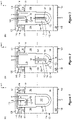
- Figure 1 illustrates a partial cross-sectional view of an embodiment of a semiconductor device 100 having enhanced charge carrier mobility in one or more targeted regions by introducing strain.
- the semiconductor device 100 may be a low voltage power MOSFET having a maximum voltage rating of 40V or below.
- the semiconductor device 100 instead may be a medium voltage power MOSFET having a maximum voltage rating between 40V and 100V.
- Other device types may utilize the contact teachings described herein, such as but not limited to IGBTs, HEMTs, etc.
- the semiconductor device 100 includes a semiconductor substrate 102.
- the semiconductor device 100 is described in the context of Si (silicon) as the semiconductor material of the substrate 102.
- the substrate 102 may comprise one or more semiconductor materials that are used to form semiconductor devices such as power MOSFETs, IGBTs, HEMTs, etc.
- the substrate 102 may include Si, silicon carbide (SiC), germanium (Ge), silicon germanium (SiGe), gallium nitride (GaN), gallium arsenide (GaAs), and the like.
- the semiconductor substrate 102 may be a bulk semiconductor material or may include one or more epitaxial layers grown on a bulk semiconductor material.
- the semiconductor device 100 further includes gate trenches 104 extending from a first main surface 101 of the semiconductor substrate 102 and into the substrate 102, and semiconductor mesas 106 between adjacent gate trenches 104. Only a single gate trench 104 is shown in Figure 1 .
- the gate trenches 104 may be 'stripe-shaped' in that the gate trenches 104 have a longest linear dimension in a direction that runs in and out of the page in Figure 1 and transverse to the depth-wise direction (z direction in Figure 1 ) of the semiconductor substrate 102.
- Each gate trench 104 contains an electrode structure that includes a gate electrode 108 disposed in the gate trench 104 and a gate dielectric insulating material 110 that separates the gate electrode 108 from the surrounding semiconductor substrate 102.
- the gate electrodes 108 are electrically connected to a gate terminal (G) of the semiconductor device 100.
- a field plate electrode 112 may be disposed in the gate trenches 104 below the gate electrodes 108 and insulated from the surrounding semiconductor substrate 102 and the gate electrodes 108 by a field dielectric insulating material 114.
- the field plates 112 instead may be disposed in different trenches (not shown) than the gate electrodes 108.
- the field plates 112 may be disposed in needle-shaped trenches that are separate from the gate trenches 104. Needle-shaped trenches are trenches that are narrow and long in a depth-wise direction (z direction in Figure 1 ) of the semiconductor substrate 102. Needle-shaped field plate trenches may resemble a needle, column or spicule in the depth-wise direction of the semiconductor substrate 102.
- the gate electrodes 108 and the field plate electrodes 112 may be made from any suitable electrically conductive material such as but not limited to polysilicon, metal (e.g., tungsten), metal alloy, etc.
- the gate electrodes 108 and the field plate electrodes 112 may comprise the same or different electrically conductive material.
- the gate dielectric insulating material 110 and the field dielectric insulating material 114 and may comprise the same or different electrically insulative material, e.g., SiOx and may be formed by one or more common processes such as but not limited to thermal oxidation and/or deposition.
- the semiconductor mesas 106 between adjacent gate trenches 104 may include a source region 116 of a first conductivity type and a body region 118 of a second conductivity type opposite the first conductivity type.
- the body region 118 may include a body contact region (not shown) of the second conductivity type and having a higher doping concentration than the body region 118, to provide an ohmic connection with a source metallization 120.
- the first conductivity is n-type and the second conductivity type is p-type for an n-channel device whereas the first conductivity is p-type and the second conductivity type is n-type for a p-channel device.
- the source region 116 and the body region 118 included in the same semiconductor mesa 106 may form part of a transistor cell, and the transistor cells may be electrically connected in parallel between source (S) and drain (D) terminals of the semiconductor device 100 to form a power transistor and as indicated by the dashed lines in Figure 1 .
- the electrode structure that includes the gate electrode 108 adjoins a channel region 122 through which current flows in a first (current flow) direction during operation of the semiconductor device 100.
- the current flow direction is in the z-direction between the first main surface 101 of the semiconductor substrate 102 and a second main surface 103 of the semiconductor substrate 102 opposite the first main surface 101.
- a drain region 124 of the first conductivity type is located at the second main surface 103 of the semiconductor substrate 102 and a drift region 126 of the first conductivity type is positioned between the drain region 124 and the body region 118.
- a metallization 128 at the second main surface 103 of the semiconductor substrate 102 forms the drain (D) terminal of the vertical power MOSFET.
- the current flow direction is in the x-direction along the first main surface 101 of the semiconductor substrate 102 and the drain region 124 is positioned at the first main surface 101 and spaced apart from the source region 116 by the drift region 126 at the first main surface 101.
- the semiconductor device 100 further includes a strain-inducing material 130 embedded in the gate electrode 108.
- the gate electrode 108 is under either tensile or compressive stress in the current flow direction, which is the z-direction in Figure 1 .
- the strain-inducing material 130 either enhances or at least partly counteracts the stress of the gate electrode 108 in the current flow direction such that the mobility of charge carriers that contribute to the current flow in the current flow direction is increased in the channel region 122.
- strain develops during processing and thermal cycling of the device. Strain may also build up due to geometrical constraints, due to material formation processes such as oxidation, silicidation, and crystallization, and due to lattice mismatch between two materials.
- strain influences electron and hole mobility due to strain-induced changes in the conductivity effective mass and scattering rate of charge carriers. From an overly simplified perspective, tensile strain along the direction of current flow increases electron mobility and decreases hole mobility whereas compressive strain along the direction of current flow increases hole mobility and decreases electron mobility.
- the strain fields in a device are extremely complex, especially near the interface of silicon and oxide.
- the strain-inducing material 130 is more compressive than the gate electrode 108 along the gate oxide interface in the current flow direction (z-direction in Figure 1 ). Accordingly, strain in the adjacent channel region 112 becomes more tensile or less compressive and either of which advantageously increase electron mobility.
- the gate electrode 108 may have a void 132, the strain-inducing material 130 may line sidewalls 134 and a bottom 136 of the void 132, and the strain-inducing material 130 may comprise silicon oxide.
- the void 132 may be filled completely with the silicon oxide.
- an inner region 138 of the void 132 spaced inward from the sidewalls 134 and the bottom 136 of the void 132 may be unfilled by the silicon oxide, e.g., as shown in Figure 1 .
- the semiconductor device 100 is a p-channel device and the strain-inducing material 130 comprises a material selected from the group consisting of silicon nitride (e.g., Si 3 N 4 ), titanium nitride (TiN), tungsten (W), and a silicide such as TiSi, CoSi, NiSi or combinations thereof.
- silicon nitride e.g., Si 3 N 4
- TiN titanium nitride
- W tungsten
- silicide such as TiSi, CoSi, NiSi or combinations thereof.
- the gate electrode 108 may comprise polysilicon. After annealing, the crystallized polysilicon is under tensile stress in the current flow direction (z-direction in Figure 1 ) and therefore introduces compressive strain into the surrounding semiconductor mesa 106 in the current flow direction. The compressive strain imparted by the gate electrode 108 limits the mobility of electrons in the adjacent semiconductor mesa 106, including in the channel region 122, which is undesirable for n-channel devices and desirable for p-channel devices.
- the tensile stress of the gate electrode 108 is at least partly counteracted by the strain-inducing material 130 in the current flow direction. At least partly counteracting the tensile stress of the gate electrode 108 in this way increases the tensile strain in the adjacent semiconductor mesa 106 along the direction of current flow between the source terminal (S) and the drain terminal (D) of the device 100.
- the strain-inducing material 130 may be under more compressive stress than the gate electrode 108 in the current flow direction.
- electron mobility is enhanced in the vertical direction for an n-channel device, including in the channel region 122, which reduces the overall on-state resistance R ON without degrading the voltage blocking capability of the device 100.
- the charge carriers that contribute to the current flow in the current flow direction are holes. Accordingly, the strain-inducing material 130 either enhances or at least partly counteracts the stress of the gate electrode 108 in the current flow direction such that strain in the channel region 122 becomes more compressive or less tensile in the current flow direction. For example, if the gate electrode 108 is under compressive stress in the current flow direction, the strain-inducing material 130 is either under less compressive stress than the gate electrode 108 or under tensile stress in the current flow direction.
- the strain-inducing material 130 is under more tensile stress than the gate electrode 108 in the current flow direction.
- hole mobility is enhanced in the vertical direction for a p-channel device, including in the channel region 122, which advantageously reduces the overall on-state resistance R ON without degrading the voltage blocking capability of the device 100.
- the electrode 108 in which the strain-inducing material 130 is embedded may be under tensile or compressive stress in the current flow direction (z-direction in Figure 1 ). In the case of tensile stress, the strain-inducing material 130 is under less tensile stress than the electrode 108 or even under compressive stress. In the case of compressive stress, the strain-inducing material 130 is under more compressive stress than the electrode 108.
- the electrode 108 may comprise n-type or p-type doped polysilicon, TiN, TiN/W stack, doped or undoped polysilicon with a silicide such as TiSi, CoSi, NiSi or combinations thereof
- the strain-inducing material 130 may comprise compressive SiO 2 formed by oxidation, TEOS (tetraethyl orthosilicate) deposition, LPCVD (low-pressure chemical vapor deposition), ALD (atomic layer deposition), radical oxidation, etc., AIN (piezoelectric material formed by ALD), AIScN (piezoelectric material formed by ALD), PZT (piezoelectric material), graphenic carbon (slightly compressive) such as sheets of graphene having an adequate distribution of sp3 and sp2 bonds where sp3 bonds enable good adhesion to adjoining layers and sp2 bonds give rise to metallicity, compressive Si 3 N 4 formed by PECVD (plasma-enhanced CVD
- the electrode 108 in which the strain-inducing material 130 is embedded may be under tensile or compressive stress in the current flow direction (z-direction in Figure 1 ).
- the strain-inducing material 130 In the case of compressive stress, the strain-inducing material 130 is under less compressive stress than the electrode 108 or even under tensile stress. In the case of tensile stress, the strain-inducing material 130 is under more tensile stress than the electrode 108.
- the electrode 108 may comprise n-type or p-type doped polysilicon, TiN, TiN/W stack, doped or undoped polysilicon with a silicide such as TiSi, CoSi, NiSi or combinations thereof, and the strain-inducing material 130 may comprise tensile Si 3 N 4 (most Si 3 N 4 deposition methods yield tensile Si 3 N 4 ), TiN formed by ALD or CVD, tungsten (W) formed by CVD, a silicide such as TiSi, CoSi, NiSi or combinations thereof.
- Figure 2 illustrates a partial cross-sectional view of another embodiment of a semiconductor device 200 having enhanced charge carrier mobility in one or more targeted regions by introducing strain.
- the embodiment illustrated in Figure 2 is similar to the embodiment illustrated in Figure 1 .
- the strain-inducing material 130 is embedded in the field plate electrode 112 instead of the gate electrode 108 of the transistor cells.
- Each field plate electrode 112 adjoins the drift region 126 of the device 200.
- the charge carriers that contribute to the current flow in the current flow direction are electrons and the strain-inducing material 130 either enhances or at least partly counteracts the stress of the field plate electrode 112 in the current flow direction such that strain in the drift region 126 becomes more tensile or less compressive in the current flow direction.
- the strain-inducing material 130 is either under less tensile stress than the field plate electrode 112 or under compressive stress in the current flow direction.
- the strain-inducing material 130 is under more compressive stress than the field plate electrode 112 in the current flow direction.
- electron mobility is enhanced in the drift region 126 in the current flow direction for an n-channel device by embedding the strain-inducing material 130 in the field plate electrode 112.
- the charge carriers that contribute to the current flow in the current flow direction are holes and the strain-inducing material 130 either enhances or at least partly counteracts the stress of the field plate electrode 112 in the current flow direction such that strain in the drift region 126 becomes more compressive or less tensile in the current flow direction.
- the strain-inducing material 130 is either under less compressive stress than the field plate electrode 112 or under tensile stress in the current flow direction.
- the strain-inducing material 130 is under more tensile stress than the field plate electrode 112 in the current flow direction.
- hole mobility is enhanced in the drift region 126 in the current flow direction for a p-channel device by embedding the strain-inducing material 130 in the field plate electrode 112.
- Figure 3 illustrates a partial cross-sectional view of another embodiment of a semiconductor device 300 having enhanced charge carrier mobility in one or more targeted regions by introducing strain.
- the embodiment illustrated in Figure 3 represents a combination of the embodiments illustrated in Figures 1 and 2 . That is, a first strain-inducing material 130' is embedded in the gate electrode 108 as in Figure 1 and a second strain-inducing material 130" is embedded in the field plate electrode 112 as in Figure 2 .
- the gate electrode 108 is under either tensile or compressive stress in the current flow direction (z-direction in Figure 3 ) and the first strain-inducing material 130' either enhances or at least partly counteracts the stress of the gate electrode 108 in the current flow direction.
- the field plate electrode 112 also is under either tensile or compressive stress in the current flow direction and the second strain-inducing material 130" either enhances or at least partly counteracts the stress of the field plate electrode 112 in the current flow direction.
- the stress and material configurations described above with reference to Figures 1 and 2 for the electrodes and strain-inducing material for both n-channel and p-channel devices also apply to the embodiment illustrated in Figure 3 .
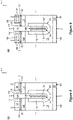
- Figure 4 illustrates a partial cross-sectional view of another embodiment of a semiconductor device 400 having enhanced charge carrier mobility in one or more targeted regions by introducing strain.
- the embodiment illustrated in Figure 4 is similar to the embodiment illustrated in Figure 1 .
- the field plate electrode 112 is disposed in a different trench 402 than the gate electrode 108.
- the field plate trenches 402 may extend deeper into the semiconductor substrate 102 than the gate trenches 104.
- the field plate trenches 402 may be needle-shaped or stripe-shaped (lines) whereas the gate trenches 104 may be stripe-shaped (lines) or shaped as a grid (array) that laterally surrounds the field plate trenches 402, for example.
- the stress and material configurations described above with reference to Figures 1 and 2 for the electrodes and strain-inducing material for both n-channel and p-channel devices also apply to the embodiment illustrated in Figure 4 .
- Figure 5 illustrates a partial cross-sectional view of another embodiment of a semiconductor device 500 having enhanced charge carrier mobility in one or more targeted regions by introducing strain.
- the embodiment illustrated in Figure 5 is similar to the embodiment illustrated in Figure 2 .
- the field plate electrode 112 is disposed in a different trench 402 than the gate electrode 108.
- the field plate trenches 402 may extend deeper into the semiconductor substrate 102 than the gate trenches 104.
- the field plate trenches 402 may be needle-shaped or stripe-shaped (lines) whereas the gate trenches 104 may be stripe-shaped or shaped as a grid that laterally surrounds the field plate trenches 402, for example.
- the stress and material configurations described above with reference to Figures 1 and 2 for the electrodes and strain-inducing material for both n-channel and p-channel devices also apply to the embodiment illustrated in Figure 4 .
- Figure 6 illustrates a partial cross-sectional view of another embodiment of a semiconductor device 600 having enhanced charge carrier mobility in one or more targeted regions by introducing strain.
- the embodiment illustrated in Figure 6 represents a combination of the embodiments illustrated in Figures 4 and 5 . That is, the field plate electrodes 112 are disposed in different trenches 402 than the gate electrodes 108, a first strain-inducing material 130' is embedded in the gate electrodes 108 as in Figure 4 , and a second strain-inducing material 130" is embedded in the field plate electrodes 112 as in Figure 5 .
- the gate electrodes 108 are under either tensile or compressive stress in the current flow direction (z-direction in Figure 6 ) and the first strain-inducing material 130' either enhances or at least partly counteracts the stress of the gate electrodes 108 in the current flow direction.
- the field plate electrodes 112 also are under either tensile or compressive stress in the current flow direction and the second strain-inducing material 130" either enhances or at least partly counteracts the stress of the field plate electrodes 112 in the current flow direction.
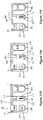
- Figure 7 illustrates a partial cross-sectional view of another embodiment of a semiconductor device 700 having enhanced charge carrier mobility in one or more targeted regions by introducing strain.
- the electrode structure is a planar gate electrode structure disposed on the first main surface 101 of the semiconductor substrate 102.
- the gate electrodes 108 are separated from the first main surface 101 of the semiconductor substrate 102 by the gate dielectric insulating material 110.
- the strain-inducing material 130 is embedded in the planar gate electrode 108.
- the semiconductor device 700 has a planar gate electrode structure, the device is still a vertical device in that the drain terminal D is disposed at the opposite side of the semiconductor substrate 102 as the source terminal S.
- the current flow path has a first (horizontal) part that traverses the channel region 122 along the horizontal gate structure in the x-direction in Figure 2 , and a second (vertical) part that traverses the drift region 126 in the z-direction to the drain terminal D.
- the planar gate electrode 108 is under either tensile or compressive stress in the horizontal part of the current flow path (x-direction in Figure 2 ) and the strain-inducing material 130 either enhances or at least partly counteracts the stress of the planar gate electrode 108 in the horizontal part of the current flow path which occurs in the channel region 122.
- the stress and material configurations described above with reference to Figures 1 and 2 for the electrodes and strain-inducing material for both n-channel and p-channel devices also apply to the embodiment illustrated in Figure 7 .
- the semiconductor device 700 illustrated in Figure 7 also includes a trench 402 formed in the semiconductor substrate 102 and a field plate electrode 112 disposed in the trench 402 and separated from the semiconductor substrate 102 by a field dielectric insulating material 114.
- the field plate 112 may be at source potential, for example.
- Figure 8 illustrates a partial cross-sectional view of another embodiment of a semiconductor device 800 having enhanced charge carrier mobility in one or more targeted regions by introducing strain.
- the embodiment illustrated in Figure 8 is similar to the embodiment illustrated in Figure 7 .
- the strain-inducing material 130 is embedded in the field plate electrode 112 instead of the planar gate electrode 108 in Figure 8 .
- the field plate electrode 112 is under either tensile or compressive stress in the second (vertical) part of the current flow path (z-direction in Figure 9 ) and the strain-inducing material 130 either enhances or at least partly counteracts the stress of the field plate electrode 112 in the vertical part of the current flow path.
- the stress and material configurations described above with reference to Figures 1 and 2 for the electrodes and strain-inducing material for both n-channel and p-channel devices also apply to the embodiment illustrated in Figure 8 .
- Figure 9 illustrates a partial cross-sectional view of another embodiment of a semiconductor device 900 having enhanced charge carrier mobility in one or more targeted regions by introducing strain.
- the embodiment illustrated in Figure 9 represents a combination of the embodiments illustrated in Figures 7 and 8 . That is, a first strain-inducing material 130' is embedded in the planar gate electrode 108 as in Figure 7 and a second strain-inducing material 130" is embedded in the field plate electrode 112 as in Figure 8 .
- the planar gate electrode 108 is under either tensile or compressive stress in the first (horizontal) part of the current flow path (x-direction in Figure 9 ) and the first strain-inducing material 130' either enhances or at least partly counteracts the stress of the planar gate electrode 108 in the horizontal part current flow path.
- the field plate electrode 112 is under either tensile or compressive stress in the second (vertical) part of the current flow path (z-direction in Figure 9 ) and the second strain-inducing material 130" either enhances or at least partly counteracts the stress of the field plate electrode 112 in the vertical part of the current flow path.
- Figure 10 illustrates a partial cross-sectional view of another embodiment of a semiconductor device 1000 having enhanced charge carrier mobility in one or more targeted regions by introducing strain.
- the embodiment illustrated in Figure 10 is similar to the embodiment illustrated in Figure 1 .
- the semiconductor device 1000 in Figure 10 does not have field plate electrodes 112 buried in trenches formed in the semiconductor substrate 102.
- the stress and material configurations described above with reference to Figures 1 and 2 for the electrodes and strain-inducing material for both n-channel and p-channel devices also apply to the embodiment illustrated in Figure 10 .
- Figure 11 illustrates a partial cross-sectional view of another embodiment of a semiconductor device 1100 having enhanced charge carrier mobility in one or more targeted regions by introducing strain.
- the strain-inducing material 130 comprises a piezoelectric material.
- An additional electrode 1102 may be embedded in the piezoelectric material, for controlling an electric field applied to the piezoelectric material.
- the electrode 108 in which the strain-inducing material 130 is embedded and the additional electrode 1102 are configured to apply an electric field to the piezoelectric material to control the strain of the strain-inducing material 130.
- An inverse piezoelectric effect yields either a contraction or expansion of the piezoelectric material under the applied electric field. That is, in the case of a piezoelectric material as the strain-inducing material 130, the enhancing or counteracting stress provided by the strain-inducing material 130 is voltage-controlled. Accordingly, the strain effect may be activated only in the on-state of the semiconductor device 1100.
- PZT lead zirconate titanate
- AIN has about ten times lower piezoelectric response than PZT but is compatible with Si technology, can be deposited by ALD with reliable step coverage, and has a piezoelectric coefficient (pm/V) of 3.54 +-0.60.
- the piezoelectric-based strain-inducing material 130 may be embedded in either the gate electrode 108, the field plate electrode 112, or both the gate electrode 108 and the field plate electrode 112 where the gate electrode 108 may be trench-type or planar-type, as previously described herein with reference to Figures 1 through 10 .
- Figures 12A through 12H illustrate partial cross-sectional views of an embodiment of embedding the strain-inducing material 130 in a field plate electrode 112.
- Figure 12A shows a semiconductor substrate 102 after forming 3 different types of trenches 1200, 1202, 1204 in the semiconductor substrate 102, lining the trenches 1200, 1202, 1204 with a first insulating material 1206 such as SiO 2 , then filling the trenches 1200, 1202, 1204 with a first electrically conductive material 1208 such as polysilicon, and recessing the first electrically conductive material 1208 including to a depth in the left and middle trenches 1200, 1202.
- a first insulating material 1206 such as SiO 2
- Figure 12B shows the semiconductor substrate 102 after a first resist 1210 is deposited over the left and right trenches 1200, 1204 and the first electrically conductive material 1208 is removed from the exposed middle trench 1202.
- Figure 12C shows the semiconductor substrate 102 after the first resist 1210 is removed and a second electrically conductive material 1212 is deposited on the exposed sidewalls of the trenches 1200, 1202, 1204 and bottom of the middle trench 1202, followed by an annealing step.
- the second electrically conductive material 1212 is thin enough such that a space 1213 remains in the middle trench 1202.
- Figure 12D shows the semiconductor substrate 102 after a second resist 1214 is deposited over the trenches 1200, 1202, 1204.
- the second resist 1214 fills the space 1213 of the middle trench 1202.
- Figure 12E shows the semiconductor substrate 102 after the second resist 1214 is recessed, leaving a segment 1214' of the second resist 1214 in the lower part of the middle trench 1202.
- Figure 12F shows the semiconductor substrate 102 after isotropic etching of the second electrically conductive material 1212, leaving a first field plate electrode 112' in the lower part of the left trench 1200, a second field plate electrode 112" in the lower part of the middle trench 1202 and a source electrode 1216 in the right trench 1204.
- the source electrode 1216 in the right trench 1204 may form part of an edge termination structure or connection structure for the buried field plates 112', 112", for example.
- Figure 12G shows the semiconductor substrate 102 after removal of the segment 1214' of the second resist 1214 previously disposed in the lower part of the middle trench 1202 and after etching of the exposed part of the first insulating material 1206.
- the part of the first insulating material 1206 that remains post-etching forms a field oxide 1218 in the trenches 1200, 1202, 1204 for separating the respective electrodes 112', 112", 1216 from the surrounding substrate 102.
- Removing the segment 1214' of the second resist 1214 from the lower part of the middle trench 1202 yields a void 132 within the second field plate electrode 112" in the middle trench 1202.
- Figure 12H shows the semiconductor substrate 102 after thermal oxidation of, or oxide deposition on, the electrodes 112', 112", 1216 and first main surface 101 of the semiconductor substrate 102.
- the oxidation process yields an oxide 1220 that lines the sidewalls and bottom of the void 132 within the second field plate electrode 112" in the middle trench 1202.
- the oxide 1220 forms the strain-inducing material 130 in this embodiment.
- an inner region 138 of the void 132 may remain unfilled by the oxide 1220, e.g., as shown in Figure 1 .
- Figures 13A through 13H illustrate partial cross-sectional views of an embodiment of embedding the strain-inducing material 130 in a gate electrode 108. The processing shown in Figures 13A through 13H continues from Figure 12H .
- Figure 13A shows the semiconductor substrate 102 after a third electrically conductive material 1222 is deposited over the first main surface 101 of the substrate 102 and plasma etched, leaving a first residual structure 1222' in the upper part of the left trench 1202 and a second residual structure 1222" in the upper part of the middle trench 1202.
- Figure 13B shows the semiconductor substrate 102 after a third resist 1224 is deposited over the left and right trenches 1200, 1204 and the second residual structure 1222" in the upper part of the exposed middle trench 1202 is removed by etching.
- Figure 13C shows the semiconductor substrate 102 after the third resist 1224 is removed and a fourth electrically conductive material 1226 is deposited over the first main surface 101 of the semiconductor substrate 102, followed by an annealing step.
- the fourth electrically conductive material 1226 covers the exposed sidewalls of the middle trench 1202 but is thin enough such that a space 1228 remains in the upper part of the middle trench 1202.
- Figure 13D shows the semiconductor substrate 102 after a fourth resist 1230 is deposited over the first main surface 101 of the substrate 102.
- the fourth resist 1230 fills the space 1228 in the upper part of the middle trench 1202.
- Figure 13E shows the semiconductor substrate 102 after the fourth resist 1230 is recessed or planarized.
- a residual part 1230' of the fourth resist 1230 remains in the space 1228 in the upper part of the middle trench 1202 after the recessing/planarizing.
- Figure 13F shows the semiconductor substrate 102 after isotropic etching of the fourth electrically conductive material 1226, leaving a first gate electrode 108' in the upper part of the left trench 1200 and a second gate electrode 108" in the upper part of the middle trench 1202.
- Figure 13G shows the semiconductor substrate 102 after removal of the residual part 1230' of the fourth resist 1230 from the space 1228 in the upper part of the middle trench 1202 and after thermal oxidation of, or oxide deposition on, the gate electrodes 108', 108" and the first main surface 101 of the semiconductor substrate 102.
- the oxidation process yields an oxide 1232 that lines the sidewalls and bottom of the void within the second gate electrode 108" formed by removing the residual part 1230' of the fourth resist 1230 from the space 1228 in the upper part of the middle trench 1202.
- the oxide 1232 forms the strain-inducing material 130 in this embodiment.
- an inner region 138 of the void may remain unfilled by the oxide 1232, e.g., as shown in Figure 1 .
- Figure 13H shows the semiconductor substrate 102 after a plasma etch process that removes the oxide 1232 from the first main surface 101 of the substrate 102.
- Example1 A semiconductor device, comprising: a semiconductor substrate; an electrode structure on or in the semiconductor substrate, the electrode structure comprising an electrode and an insulating material that separates the electrode from the semiconductor substrate; and a strain-inducing material embedded in the electrode, wherein the electrode structure adjoins a region of the semiconductor substrate through which current flows in a first direction during operation of the semiconductor device, wherein the electrode is under either tensile or compressive stress in the first direction, wherein the strain-inducing material either enhances or at least partly counteracts the stress of the electrode in the first direction.
- Example 2 The semiconductor device of example 1, wherein the electrode is a gate electrode, and wherein the region of the semiconductor substrate that adjoins the electrode structure is a channel region.
- Example 3 The semiconductor device of example 2, wherein the semiconductor device is an n-channel device, wherein the charge carriers that contribute to the current flow in the first direction are electrons, and wherein the strain-inducing material either enhances or at least partly counteracts the stress of the gate electrode in the first direction such that strain in the channel region becomes more tensile or less compressive in the first direction.
- Example 4 The semiconductor device of example 3, wherein the gate electrode is under tensile stress in the first direction, and wherein the strain-inducing material is either under less tensile stress than the gate electrode or under compressive stress in the first direction.
- Example 5 The semiconductor device of example 3, wherein the gate electrode is under compressive stress in the first direction, and wherein the strain-inducing material is under more compressive stress than the gate electrode in the first direction.
- Example 6 The semiconductor device of example 2, wherein the semiconductor device is a p-channel device, wherein the charge carriers that contribute to the current flow in the first direction are holes, and wherein the strain-inducing material either enhances or at least partly counteracts the stress of the gate electrode in the first direction such that strain in the channel region becomes more compressive or less tensile in the first direction.
- Example 7 The semiconductor device of example 6, wherein the gate electrode is under compressive stress in the first direction, and wherein the strain-inducing material is either under less compressive stress than the gate electrode or under tensile stress in the first direction.
- Example 8 The semiconductor device of example 6, wherein the gate electrode is under tensile stress in the first direction, and wherein the strain-inducing material is under more tensile stress than the gate electrode in the first direction.
- Example 9 The semiconductor device of any of examples 2 through 8, wherein the gate electrode is disposed in a trench formed in the semiconductor substrate, and wherein the trench further includes a field plate electrode disposed below the gate electrode and insulated from the gate electrode.
- Example 10 The semiconductor device of example 9, further comprising: an additional strain-inducing material embedded in the field plate electrode, wherein the field plate electrode adjoins a drift region of the semiconductor substrate, wherein the field plate electrode is under either tensile or compressive stress in the first direction, wherein the additional strain-inducing material either enhances or at least partly counteracts the stress of the field plate electrode in the first direction.
- Example 11 The semiconductor device of any of examples 2 through 8, wherein the gate electrode is disposed in a first trench formed in the semiconductor substrate, wherein a field plate electrode is disposed in a second trench formed in the semiconductor substrate, and wherein the first trench and the second trench are laterally spaced apart from one another.
- Example 12 The semiconductor device of example 11, further comprising: an additional strain-inducing material embedded in the field plate electrode, wherein the field plate electrode adjoins a drift region of the semiconductor substrate, wherein the field plate electrode is under either tensile or compressive stress in the first direction, wherein the additional strain-inducing material either enhances or at least partly counteracts the stress of the field plate electrode in the first direction.
- Example 13 The semiconductor device of any of examples 1 through 8, wherein the electrode structure is a planar gate electrode structure disposed on a first main surface of the semiconductor substrate, wherein the electrode is a gate electrode, and wherein the insulating material separates the gate electrode from the first main surface of the semiconductor substrate.
- Example 14 The semiconductor device of example 13, further comprising: a trench formed in the semiconductor substrate; a field plate electrode in the trench and separated from the semiconductor substrate by an additional insulating material.
- Example 15 The semiconductor device of example 14, further comprising: an additional strain-inducing material embedded in the field plate electrode, wherein the field plate electrode is under either tensile or compressive stress in the first direction, wherein the additional strain-inducing material either enhances or at least partly counteracts the stress of the field plate electrode in the first direction.
- Example 16 The semiconductor device of example 1, wherein the electrode is a field plate electrode, wherein the field plate electrode is disposed in a trench formed in the semiconductor substrate, and wherein the region of the semiconductor substrate that adjoins the electrode structure is a drift region.
- Example 17 The semiconductor device of example 16, wherein the semiconductor device is an n-channel device, wherein the charge carriers that contribute to the current flow in the first direction are electrons, and wherein the strain-inducing material either enhances or at least partly counteracts the stress of the field plate electrode in the first direction such that strain in the drift region becomes more tensile or less compressive in the first direction.
- Example 18 The semiconductor device of example 17, wherein the field plate electrode is under tensile stress in the first direction, and wherein the strain-inducing material is either under less tensile stress than the field plate electrode or under compressive stress in the first direction.
- Example 19 The semiconductor device of example 17, wherein the field plate electrode is under compressive stress in the first direction, and wherein the strain-inducing material is under more compressive stress than the field plate electrode in the first direction.
- Example 20 The semiconductor device of example 16, wherein the semiconductor device is a p-channel device, wherein the charge carriers that contribute to the current flow in the first direction are holes, and wherein the strain-inducing material either enhances or at least partly counteracts the stress of the field plate electrode in the first direction such that strain in the drift region becomes more compressive or less tensile in the first direction.
- Example 21 The semiconductor device of example 20, wherein the field plate electrode is under compressive stress in the first direction, and wherein the strain-inducing material is either under less compressive stress than the field plate electrode or under tensile stress in the first direction.
- Example 22 The semiconductor device of example 21, wherein the field plate electrode is under tensile stress in the first direction, and wherein the strain-inducing material is under more tensile stress than the field plate electrode in the first direction.
- Example 23 The semiconductor device of any of examples 16 through 22, wherein the trench further includes a gate electrode disposed above the field plate electrode and insulated from the field plate electrode.
- Example 24 The semiconductor device of any of examples 16 through 22, wherein a gate electrode is disposed in an additional trench formed in the semiconductor substrate, and wherein the trench and the additional trench are laterally spaced apart from one another.
- Example 25 The semiconductor device of any of examples 1 through 5, 9 through 19 and 23 through 24, wherein the semiconductor device is an n-channel device, and wherein the strain-inducing material comprises a material selected from the group consisting of silicon oxide, silicon nitride, a piezoelectric material, and graphenic carbon.
- Example 26 The semiconductor device of any of examples 1 through 25, wherein the electrode has a void, wherein the strain-inducing material lines sidewalls and a bottom of the void, and wherein the strain-inducing material comprises silicon oxide.
- Example 27 The semiconductor device of example 26, wherein the void in the electrode is filled completely with the silicon oxide.
- Example 28 The semiconductor device of example 27, wherein an inner region of the void spaced inward from the sidewalls and the bottom of the void is unfilled by the silicon oxide.
- Example 29 The semiconductor device of any of examples 1 through 2, 6 through 16 and 20 through 24, wherein the semiconductor device is a p-channel device, and wherein the strain-inducing material comprises a material selected from the group consisting of silicon nitride, titanium nitride, tungsten, and a silicide.
- Example 30 The semiconductor device of any of examples 1 through 29, wherein the strain-inducing material comprises a piezoelectric material, wherein the electrode structure comprises an additional electrode embedded in the piezoelectric material, and wherein the electrode and the additional electrode are configured to apply an electric field to the piezoelectric material to control the strain of the strain-inducing material.
Landscapes
- Electrodes Of Semiconductors (AREA)
- Engineering & Computer Science (AREA)
- Chemical & Material Sciences (AREA)
- Materials Engineering (AREA)
- Manufacturing & Machinery (AREA)
Abstract
Description
- Performance enhancement for power semiconductor devices such as power MOSFETs (metal-oxide-semiconductor field-effect transistors), IGBTs (insulated gate bipolar transistors), HEMTs (high-electron mobility transistors), etc. is typically achieved by reducing the device dimensions. However, tooling, process and material constraints limit the amount by which device dimensions can be further reduced.
- Thus, there is a need for new techniques for enhancing the performance of power semiconductor devices.
- According to an embodiment of a semiconductor device, the semiconductor device comprises: a semiconductor substrate; an electrode structure on or in the semiconductor substrate, the electrode structure comprising an electrode and an insulating material that separates the electrode from the semiconductor substrate; and a strain-inducing material embedded in the electrode, wherein the electrode structure adjoins a region of the semiconductor substrate through which current flows in a first direction during operation of the semiconductor device, wherein the electrode is under either tensile or compressive stress in the first direction, wherein the strain-inducing material either enhances or at least partly counteracts the stress of the electrode in the first direction.
- Those skilled in the art will recognize additional features and advantages upon reading the following detailed description, and upon viewing the accompanying drawings.
- The elements of the drawings are not necessarily to scale relative to each other. Like reference numerals designate corresponding similar parts. The features of the various illustrated embodiments can be combined unless they exclude each other. Embodiments are depicted in the drawings and are detailed in the description which follows.
-
Figures 1 through 11 illustrate respective partial cross-sectional views of semiconductor devices each having enhanced charge carrier mobility in one or more targeted regions by introducing strain, according to different embodiments. -
Figures 12A through 12H illustrate partial cross-sectional views of an embodiment of embedding a strain-inducing material in a field plate electrode. -
Figures 13A through 13H illustrate partial cross-sectional views of an embodiment of embedding a strain-inducing material in a gate electrode. - The embodiments described herein enhance charge carrier mobility in power semiconductor devices by embedding a strain-inducing material in an electrode of an electrode structure. The electrode structure adjoins a region of the power semiconductor device through which current flows in a current flow direction during operation of the device. For example, the electrode may be a planar or trench gate electrode used to control the current flow in a channel region of the device. In another example, the electrode may be a field plate electrode used to reduce area-dependent on-state resistance in a drain region of the device. In either case, the electrode with the embedded strain-inducing material is under either tensile or compressive stress in the first (current flow) direction. The strain-inducing material either enhances or at least partly counteracts the stress of the electrode in the current flow direction such that a mobility of charge carriers that contribute to the current flow is increased in the region of the semiconductor substrate that adjoins the electrode structure.
- Described next with reference to the figures are embodiments of the improved contact structure and corresponding methods of production.
-
Figure 1 illustrates a partial cross-sectional view of an embodiment of asemiconductor device 100 having enhanced charge carrier mobility in one or more targeted regions by introducing strain. Thesemiconductor device 100 may be a low voltage power MOSFET having a maximum voltage rating of 40V or below. Thesemiconductor device 100 instead may be a medium voltage power MOSFET having a maximum voltage rating between 40V and 100V. Other device types may utilize the contact teachings described herein, such as but not limited to IGBTs, HEMTs, etc. - The
semiconductor device 100 includes asemiconductor substrate 102. Thesemiconductor device 100 is described in the context of Si (silicon) as the semiconductor material of thesubstrate 102. In general, thesubstrate 102 may comprise one or more semiconductor materials that are used to form semiconductor devices such as power MOSFETs, IGBTs, HEMTs, etc. For example, thesubstrate 102 may include Si, silicon carbide (SiC), germanium (Ge), silicon germanium (SiGe), gallium nitride (GaN), gallium arsenide (GaAs), and the like. Thesemiconductor substrate 102 may be a bulk semiconductor material or may include one or more epitaxial layers grown on a bulk semiconductor material. - The
semiconductor device 100 further includesgate trenches 104 extending from a firstmain surface 101 of thesemiconductor substrate 102 and into thesubstrate 102, andsemiconductor mesas 106 betweenadjacent gate trenches 104. Only asingle gate trench 104 is shown inFigure 1 . Thegate trenches 104 may be 'stripe-shaped' in that thegate trenches 104 have a longest linear dimension in a direction that runs in and out of the page inFigure 1 and transverse to the depth-wise direction (z direction inFigure 1 ) of thesemiconductor substrate 102. - Each
gate trench 104 contains an electrode structure that includes agate electrode 108 disposed in thegate trench 104 and a gate dielectricinsulating material 110 that separates thegate electrode 108 from the surroundingsemiconductor substrate 102. Thegate electrodes 108 are electrically connected to a gate terminal (G) of thesemiconductor device 100. - A
field plate electrode 112 may be disposed in thegate trenches 104 below thegate electrodes 108 and insulated from the surroundingsemiconductor substrate 102 and thegate electrodes 108 by a field dielectricinsulating material 114. Thefield plates 112 instead may be disposed in different trenches (not shown) than thegate electrodes 108. For example, thefield plates 112 may be disposed in needle-shaped trenches that are separate from thegate trenches 104. Needle-shaped trenches are trenches that are narrow and long in a depth-wise direction (z direction inFigure 1 ) of thesemiconductor substrate 102. Needle-shaped field plate trenches may resemble a needle, column or spicule in the depth-wise direction of thesemiconductor substrate 102. - The
gate electrodes 108 and thefield plate electrodes 112 may be made from any suitable electrically conductive material such as but not limited to polysilicon, metal (e.g., tungsten), metal alloy, etc. Thegate electrodes 108 and thefield plate electrodes 112 may comprise the same or different electrically conductive material. The gate dielectricinsulating material 110 and the field dielectricinsulating material 114 and may comprise the same or different electrically insulative material, e.g., SiOx and may be formed by one or more common processes such as but not limited to thermal oxidation and/or deposition. - The
semiconductor mesas 106 betweenadjacent gate trenches 104 may include asource region 116 of a first conductivity type and abody region 118 of a second conductivity type opposite the first conductivity type. Thebody region 118 may include a body contact region (not shown) of the second conductivity type and having a higher doping concentration than thebody region 118, to provide an ohmic connection with asource metallization 120. The first conductivity is n-type and the second conductivity type is p-type for an n-channel device whereas the first conductivity is p-type and the second conductivity type is n-type for a p-channel device. For either n-channel or p-channel devices, thesource region 116 and thebody region 118 included in thesame semiconductor mesa 106 may form part of a transistor cell, and the transistor cells may be electrically connected in parallel between source (S) and drain (D) terminals of thesemiconductor device 100 to form a power transistor and as indicated by the dashed lines inFigure 1 . - The electrode structure that includes the
gate electrode 108 adjoins achannel region 122 through which current flows in a first (current flow) direction during operation of thesemiconductor device 100. In the case of a vertical power MOSFET as shown inFigure 1 , the current flow direction is in the z-direction between the firstmain surface 101 of thesemiconductor substrate 102 and a secondmain surface 103 of thesemiconductor substrate 102 opposite the firstmain surface 101. In this case, adrain region 124 of the first conductivity type is located at the secondmain surface 103 of thesemiconductor substrate 102 and adrift region 126 of the first conductivity type is positioned between thedrain region 124 and thebody region 118. Ametallization 128 at the secondmain surface 103 of thesemiconductor substrate 102 forms the drain (D) terminal of the vertical power MOSFET. In the case of a lateral power transistor, the current flow direction is in the x-direction along the firstmain surface 101 of thesemiconductor substrate 102 and thedrain region 124 is positioned at the firstmain surface 101 and spaced apart from thesource region 116 by thedrift region 126 at the firstmain surface 101. - Regardless of the type of power transistor implemented by the transistor cells, and according to the embodiment illustrated in
Figure 1 , thesemiconductor device 100 further includes a strain-inducingmaterial 130 embedded in thegate electrode 108. Thegate electrode 108 is under either tensile or compressive stress in the current flow direction, which is the z-direction inFigure 1 . The strain-inducingmaterial 130 either enhances or at least partly counteracts the stress of thegate electrode 108 in the current flow direction such that the mobility of charge carriers that contribute to the current flow in the current flow direction is increased in thechannel region 122. - Due to the use of increasingly complex material stacks with different elastic and thermal properties to fabricate semiconductor devices, strain develops during processing and thermal cycling of the device. Strain may also build up due to geometrical constraints, due to material formation processes such as oxidation, silicidation, and crystallization, and due to lattice mismatch between two materials.
- In all semiconductor materials, strain influences electron and hole mobility due to strain-induced changes in the conductivity effective mass and scattering rate of charge carriers. From an overly simplified perspective, tensile strain along the direction of current flow increases electron mobility and decreases hole mobility whereas compressive strain along the direction of current flow increases hole mobility and decreases electron mobility. In practice, the strain fields in a device are extremely complex, especially near the interface of silicon and oxide.
- To enhance electron mobility in an n-channel power MOSFET, the strain-inducing
material 130 is more compressive than thegate electrode 108 along the gate oxide interface in the current flow direction (z-direction inFigure 1 ). Accordingly, strain in theadjacent channel region 112 becomes more tensile or less compressive and either of which advantageously increase electron mobility. In one embodiment, thegate electrode 108 may have avoid 132, the strain-inducingmaterial 130 mayline sidewalls 134 and abottom 136 of thevoid 132, and the strain-inducingmaterial 130 may comprise silicon oxide. The void 132 may be filled completely with the silicon oxide. Alternatively, aninner region 138 of the void 132 spaced inward from thesidewalls 134 and thebottom 136 of the void 132 may be unfilled by the silicon oxide, e.g., as shown inFigure 1 . - For a p-channel power MOSFET, hole mobility enhancement is provided by the strain-inducing
material 130 having tensile stress in the current flow direction (z-direction inFigure 1 ). Accordingly, strain in theadjacent channel region 112 becomes more compressive or less tensile and either of which advantageously increase hole mobility. In one embodiment, thesemiconductor device 100 is a p-channel device and the strain-inducingmaterial 130 comprises a material selected from the group consisting of silicon nitride (e.g., Si3N4), titanium nitride (TiN), tungsten (W), and a silicide such as TiSi, CoSi, NiSi or combinations thereof. - In some cases, the
gate electrode 108 may comprise polysilicon. After annealing, the crystallized polysilicon is under tensile stress in the current flow direction (z-direction inFigure 1 ) and therefore introduces compressive strain into the surroundingsemiconductor mesa 106 in the current flow direction. The compressive strain imparted by thegate electrode 108 limits the mobility of electrons in theadjacent semiconductor mesa 106, including in thechannel region 122, which is undesirable for n-channel devices and desirable for p-channel devices. - For an n-channel device and by embedding a strain-inducing
material 130 into thegate electrode 108 that is either under less tensile stress than thegate electrode 108 or under compressive stress in the current flow direction (z-direction inFigure 1 ), the tensile stress of thegate electrode 108 is at least partly counteracted by the strain-inducingmaterial 130 in the current flow direction. At least partly counteracting the tensile stress of thegate electrode 108 in this way increases the tensile strain in theadjacent semiconductor mesa 106 along the direction of current flow between the source terminal (S) and the drain terminal (D) of thedevice 100. - If instead the
gate electrode 108 is under compressive stress and thereby introduces tensile strain into the surroundingsemiconductor mesa 106 in the current flow direction (z-direction inFigure 1 ), the strain-inducingmaterial 130 may be under more compressive stress than thegate electrode 108 in the current flow direction. In both cases, electron mobility is enhanced in the vertical direction for an n-channel device, including in thechannel region 122, which reduces the overall on-state resistance RON without degrading the voltage blocking capability of thedevice 100. - For a p-channel device, the charge carriers that contribute to the current flow in the current flow direction (z-direction in
Figure 1 ) are holes. Accordingly, the strain-inducingmaterial 130 either enhances or at least partly counteracts the stress of thegate electrode 108 in the current flow direction such that strain in thechannel region 122 becomes more compressive or less tensile in the current flow direction. For example, if thegate electrode 108 is under compressive stress in the current flow direction, the strain-inducingmaterial 130 is either under less compressive stress than thegate electrode 108 or under tensile stress in the current flow direction. If instead thegate electrode 108 is under tensile stress in the current flow direction, the strain-inducingmaterial 130 is under more tensile stress than thegate electrode 108 in the current flow direction. In both cases, hole mobility is enhanced in the vertical direction for a p-channel device, including in thechannel region 122, which advantageously reduces the overall on-state resistance RON without degrading the voltage blocking capability of thedevice 100. - For n-channel devices in general, the
electrode 108 in which the strain-inducingmaterial 130 is embedded may be under tensile or compressive stress in the current flow direction (z-direction inFigure 1 ). In the case of tensile stress, the strain-inducingmaterial 130 is under less tensile stress than theelectrode 108 or even under compressive stress. In the case of compressive stress, the strain-inducingmaterial 130 is under more compressive stress than theelectrode 108. For example, theelectrode 108 may comprise n-type or p-type doped polysilicon, TiN, TiN/W stack, doped or undoped polysilicon with a silicide such as TiSi, CoSi, NiSi or combinations thereof, and the strain-inducingmaterial 130 may comprise compressive SiO2 formed by oxidation, TEOS (tetraethyl orthosilicate) deposition, LPCVD (low-pressure chemical vapor deposition), ALD (atomic layer deposition), radical oxidation, etc., AIN (piezoelectric material formed by ALD), AIScN (piezoelectric material formed by ALD), PZT (piezoelectric material), graphenic carbon (slightly compressive) such as sheets of graphene having an adequate distribution of sp3 and sp2 bonds where sp3 bonds enable good adhesion to adjoining layers and sp2 bonds give rise to metallicity, compressive Si3N4 formed by PECVD (plasma-enhanced CVD), etc. - For p-channel devices in general, the
electrode 108 in which the strain-inducingmaterial 130 is embedded may be under tensile or compressive stress in the current flow direction (z-direction inFigure 1 ). In the case of compressive stress, the strain-inducingmaterial 130 is under less compressive stress than theelectrode 108 or even under tensile stress. In the case of tensile stress, the strain-inducingmaterial 130 is under more tensile stress than theelectrode 108. For example, theelectrode 108 may comprise n-type or p-type doped polysilicon, TiN, TiN/W stack, doped or undoped polysilicon with a silicide such as TiSi, CoSi, NiSi or combinations thereof, and the strain-inducingmaterial 130 may comprise tensile Si3N4 (most Si3N4 deposition methods yield tensile Si3N4), TiN formed by ALD or CVD, tungsten (W) formed by CVD, a silicide such as TiSi, CoSi, NiSi or combinations thereof. -
Figure 2 illustrates a partial cross-sectional view of another embodiment of asemiconductor device 200 having enhanced charge carrier mobility in one or more targeted regions by introducing strain. The embodiment illustrated inFigure 2 is similar to the embodiment illustrated inFigure 1 . Different, however, the strain-inducingmaterial 130 is embedded in thefield plate electrode 112 instead of thegate electrode 108 of the transistor cells. Eachfield plate electrode 112 adjoins thedrift region 126 of thedevice 200. - If the
semiconductor device 200 is an n-channel device, the charge carriers that contribute to the current flow in the current flow direction (z-direction inFigure 2 ) are electrons and the strain-inducingmaterial 130 either enhances or at least partly counteracts the stress of thefield plate electrode 112 in the current flow direction such that strain in thedrift region 126 becomes more tensile or less compressive in the current flow direction. For example, if thefield plate electrode 112 is under tensile stress in the current flow direction, the strain-inducingmaterial 130 is either under less tensile stress than thefield plate electrode 112 or under compressive stress in the current flow direction. Conversely, if thefield plate electrode 112 is under compressive stress in the current flow direction, the strain-inducingmaterial 130 is under more compressive stress than thefield plate electrode 112 in the current flow direction. In both field electrode stress cases, electron mobility is enhanced in thedrift region 126 in the current flow direction for an n-channel device by embedding the strain-inducingmaterial 130 in thefield plate electrode 112. - If the
semiconductor device 200 is a p-channel device, the charge carriers that contribute to the current flow in the current flow direction (z-direction inFigure 2 ) are holes and the strain-inducingmaterial 130 either enhances or at least partly counteracts the stress of thefield plate electrode 112 in the current flow direction such that strain in thedrift region 126 becomes more compressive or less tensile in the current flow direction. For example, if thefield plate electrode 112 is under compressive stress in the current flow direction, the strain-inducingmaterial 130 is either under less compressive stress than thefield plate electrode 112 or under tensile stress in the current flow direction. Conversely, if thefield plate electrode 112 is under tensile stress in the current flow direction, the strain-inducingmaterial 130 is under more tensile stress than thefield plate electrode 112 in the current flow direction. In both field electrode stress cases, hole mobility is enhanced in thedrift region 126 in the current flow direction for a p-channel device by embedding the strain-inducingmaterial 130 in thefield plate electrode 112. -
Figure 3 illustrates a partial cross-sectional view of another embodiment of asemiconductor device 300 having enhanced charge carrier mobility in one or more targeted regions by introducing strain. The embodiment illustrated inFigure 3 represents a combination of the embodiments illustrated inFigures 1 and 2 . That is, a first strain-inducing material 130' is embedded in thegate electrode 108 as inFigure 1 and a second strain-inducingmaterial 130" is embedded in thefield plate electrode 112 as inFigure 2 . Thegate electrode 108 is under either tensile or compressive stress in the current flow direction (z-direction inFigure 3 ) and the first strain-inducing material 130' either enhances or at least partly counteracts the stress of thegate electrode 108 in the current flow direction. Similarly, thefield plate electrode 112 also is under either tensile or compressive stress in the current flow direction and the second strain-inducingmaterial 130" either enhances or at least partly counteracts the stress of thefield plate electrode 112 in the current flow direction. The stress and material configurations described above with reference toFigures 1 and 2 for the electrodes and strain-inducing material for both n-channel and p-channel devices also apply to the embodiment illustrated inFigure 3 . -
Figure 4 illustrates a partial cross-sectional view of another embodiment of asemiconductor device 400 having enhanced charge carrier mobility in one or more targeted regions by introducing strain. The embodiment illustrated inFigure 4 is similar to the embodiment illustrated inFigure 1 . Different, however, thefield plate electrode 112 is disposed in adifferent trench 402 than thegate electrode 108. Thefield plate trenches 402 may extend deeper into thesemiconductor substrate 102 than thegate trenches 104. Thefield plate trenches 402 may be needle-shaped or stripe-shaped (lines) whereas thegate trenches 104 may be stripe-shaped (lines) or shaped as a grid (array) that laterally surrounds thefield plate trenches 402, for example. The stress and material configurations described above with reference toFigures 1 and 2 for the electrodes and strain-inducing material for both n-channel and p-channel devices also apply to the embodiment illustrated inFigure 4 . -
Figure 5 illustrates a partial cross-sectional view of another embodiment of asemiconductor device 500 having enhanced charge carrier mobility in one or more targeted regions by introducing strain. The embodiment illustrated inFigure 5 is similar to the embodiment illustrated inFigure 2 . Different, however, thefield plate electrode 112 is disposed in adifferent trench 402 than thegate electrode 108. Thefield plate trenches 402 may extend deeper into thesemiconductor substrate 102 than thegate trenches 104. Thefield plate trenches 402 may be needle-shaped or stripe-shaped (lines) whereas thegate trenches 104 may be stripe-shaped or shaped as a grid that laterally surrounds thefield plate trenches 402, for example. The stress and material configurations described above with reference toFigures 1 and 2 for the electrodes and strain-inducing material for both n-channel and p-channel devices also apply to the embodiment illustrated inFigure 4 . -
Figure 6 illustrates a partial cross-sectional view of another embodiment of asemiconductor device 600 having enhanced charge carrier mobility in one or more targeted regions by introducing strain. The embodiment illustrated inFigure 6 represents a combination of the embodiments illustrated inFigures 4 and 5 . That is, thefield plate electrodes 112 are disposed indifferent trenches 402 than thegate electrodes 108, a first strain-inducing material 130' is embedded in thegate electrodes 108 as inFigure 4 , and a second strain-inducingmaterial 130" is embedded in thefield plate electrodes 112 as inFigure 5 . Thegate electrodes 108 are under either tensile or compressive stress in the current flow direction (z-direction inFigure 6 ) and the first strain-inducing material 130' either enhances or at least partly counteracts the stress of thegate electrodes 108 in the current flow direction. Similarly, thefield plate electrodes 112 also are under either tensile or compressive stress in the current flow direction and the second strain-inducingmaterial 130" either enhances or at least partly counteracts the stress of thefield plate electrodes 112 in the current flow direction. The stress and material configurations described above with reference toFigures 1 and 2 for the electrodes and strain-inducing material for both n-channel and p-channel devices also apply to the embodiment illustrated inFigure 6 . -
Figure 7 illustrates a partial cross-sectional view of another embodiment of asemiconductor device 700 having enhanced charge carrier mobility in one or more targeted regions by introducing strain. According to this embodiment, the electrode structure is a planar gate electrode structure disposed on the firstmain surface 101 of thesemiconductor substrate 102. Thegate electrodes 108 are separated from the firstmain surface 101 of thesemiconductor substrate 102 by the gate dielectric insulatingmaterial 110. The strain-inducingmaterial 130 is embedded in theplanar gate electrode 108. Although thesemiconductor device 700 has a planar gate electrode structure, the device is still a vertical device in that the drain terminal D is disposed at the opposite side of thesemiconductor substrate 102 as the source terminal S. The current flow path has a first (horizontal) part that traverses thechannel region 122 along the horizontal gate structure in the x-direction inFigure 2 , and a second (vertical) part that traverses thedrift region 126 in the z-direction to the drain terminal D. Theplanar gate electrode 108 is under either tensile or compressive stress in the horizontal part of the current flow path (x-direction inFigure 2 ) and the strain-inducingmaterial 130 either enhances or at least partly counteracts the stress of theplanar gate electrode 108 in the horizontal part of the current flow path which occurs in thechannel region 122. The stress and material configurations described above with reference toFigures 1 and 2 for the electrodes and strain-inducing material for both n-channel and p-channel devices also apply to the embodiment illustrated inFigure 7 . - The
semiconductor device 700 illustrated inFigure 7 also includes atrench 402 formed in thesemiconductor substrate 102 and afield plate electrode 112 disposed in thetrench 402 and separated from thesemiconductor substrate 102 by a field dielectric insulatingmaterial 114. Thefield plate 112 may be at source potential, for example. -
Figure 8 illustrates a partial cross-sectional view of another embodiment of asemiconductor device 800 having enhanced charge carrier mobility in one or more targeted regions by introducing strain. The embodiment illustrated inFigure 8 is similar to the embodiment illustrated inFigure 7 . Different, however, the strain-inducingmaterial 130 is embedded in thefield plate electrode 112 instead of theplanar gate electrode 108 inFigure 8 . Thefield plate electrode 112 is under either tensile or compressive stress in the second (vertical) part of the current flow path (z-direction inFigure 9 ) and the strain-inducingmaterial 130 either enhances or at least partly counteracts the stress of thefield plate electrode 112 in the vertical part of the current flow path. The stress and material configurations described above with reference toFigures 1 and 2 for the electrodes and strain-inducing material for both n-channel and p-channel devices also apply to the embodiment illustrated inFigure 8 . -
Figure 9 illustrates a partial cross-sectional view of another embodiment of asemiconductor device 900 having enhanced charge carrier mobility in one or more targeted regions by introducing strain. The embodiment illustrated inFigure 9 represents a combination of the embodiments illustrated inFigures 7 and8 . That is, a first strain-inducing material 130' is embedded in theplanar gate electrode 108 as inFigure 7 and a second strain-inducingmaterial 130" is embedded in thefield plate electrode 112 as inFigure 8 . Theplanar gate electrode 108 is under either tensile or compressive stress in the first (horizontal) part of the current flow path (x-direction inFigure 9 ) and the first strain-inducing material 130' either enhances or at least partly counteracts the stress of theplanar gate electrode 108 in the horizontal part current flow path. Thefield plate electrode 112 is under either tensile or compressive stress in the second (vertical) part of the current flow path (z-direction inFigure 9 ) and the second strain-inducingmaterial 130" either enhances or at least partly counteracts the stress of thefield plate electrode 112 in the vertical part of the current flow path. The stress and material configurations described above with reference toFigures 1 and 2 for the electrodes and strain-inducing material for both n-channel and p-channel devices also apply to the embodiment illustrated inFigure 3 . -
Figure 10 illustrates a partial cross-sectional view of another embodiment of asemiconductor device 1000 having enhanced charge carrier mobility in one or more targeted regions by introducing strain. The embodiment illustrated inFigure 10 is similar to the embodiment illustrated inFigure 1 . Different, however, thesemiconductor device 1000 inFigure 10 does not havefield plate electrodes 112 buried in trenches formed in thesemiconductor substrate 102. The stress and material configurations described above with reference toFigures 1 and 2 for the electrodes and strain-inducing material for both n-channel and p-channel devices also apply to the embodiment illustrated inFigure 10 . -
Figure 11 illustrates a partial cross-sectional view of another embodiment of asemiconductor device 1100 having enhanced charge carrier mobility in one or more targeted regions by introducing strain. According to this embodiment, the strain-inducingmaterial 130 comprises a piezoelectric material. Anadditional electrode 1102 may be embedded in the piezoelectric material, for controlling an electric field applied to the piezoelectric material. - The
electrode 108 in which the strain-inducingmaterial 130 is embedded and theadditional electrode 1102 are configured to apply an electric field to the piezoelectric material to control the strain of the strain-inducingmaterial 130. An inverse piezoelectric effect yields either a contraction or expansion of the piezoelectric material under the applied electric field. That is, in the case of a piezoelectric material as the strain-inducingmaterial 130, the enhancing or counteracting stress provided by the strain-inducingmaterial 130 is voltage-controlled. Accordingly, the strain effect may be activated only in the on-state of thesemiconductor device 1100. In the case of PZT (lead zirconate titanate) as the piezoelectric material, PZT has a high piezoelectric response but is not compatible with Si technology. Accordingly, a seed layer may be required if PZT is used as the strain-inducingmaterial 130. In the case of AIN as the piezoelectric material, AIN has about ten times lower piezoelectric response than PZT but is compatible with Si technology, can be deposited by ALD with reliable step coverage, and has a piezoelectric coefficient (pm/V) of 3.54 +-0.60. In general, the piezoelectric-based strain-inducingmaterial 130 may be embedded in either thegate electrode 108, thefield plate electrode 112, or both thegate electrode 108 and thefield plate electrode 112 where thegate electrode 108 may be trench-type or planar-type, as previously described herein with reference toFigures 1 through 10 . -
Figures 12A through 12H illustrate partial cross-sectional views of an embodiment of embedding the strain-inducingmaterial 130 in afield plate electrode 112. -
Figure 12A shows asemiconductor substrate 102 after forming 3 different types oftrenches semiconductor substrate 102, lining thetrenches material 1206 such as SiO2, then filling thetrenches conductive material 1208 such as polysilicon, and recessing the first electricallyconductive material 1208 including to a depth in the left andmiddle trenches -
Figure 12B shows thesemiconductor substrate 102 after a first resist 1210 is deposited over the left andright trenches conductive material 1208 is removed from the exposedmiddle trench 1202. -
Figure 12C shows thesemiconductor substrate 102 after the first resist 1210 is removed and a second electricallyconductive material 1212 is deposited on the exposed sidewalls of thetrenches middle trench 1202, followed by an annealing step. The second electricallyconductive material 1212 is thin enough such that aspace 1213 remains in themiddle trench 1202. -
Figure 12D shows thesemiconductor substrate 102 after a second resist 1214 is deposited over thetrenches space 1213 of themiddle trench 1202. -
Figure 12E shows thesemiconductor substrate 102 after the second resist 1214 is recessed, leaving a segment 1214' of the second resist 1214 in the lower part of themiddle trench 1202. -
Figure 12F shows thesemiconductor substrate 102 after isotropic etching of the second electricallyconductive material 1212, leaving a first field plate electrode 112' in the lower part of theleft trench 1200, a secondfield plate electrode 112" in the lower part of themiddle trench 1202 and asource electrode 1216 in theright trench 1204. Thesource electrode 1216 in theright trench 1204 may form part of an edge termination structure or connection structure for the buriedfield plates 112', 112", for example. -
Figure 12G shows thesemiconductor substrate 102 after removal of the segment 1214' of the second resist 1214 previously disposed in the lower part of themiddle trench 1202 and after etching of the exposed part of the first insulatingmaterial 1206. The part of the first insulatingmaterial 1206 that remains post-etching forms afield oxide 1218 in thetrenches respective electrodes 112', 112", 1216 from the surroundingsubstrate 102. Removing the segment 1214' of the second resist 1214 from the lower part of themiddle trench 1202 yields a void 132 within the secondfield plate electrode 112" in themiddle trench 1202. -
Figure 12H shows thesemiconductor substrate 102 after thermal oxidation of, or oxide deposition on, theelectrodes 112', 112", 1216 and firstmain surface 101 of thesemiconductor substrate 102. The oxidation process yields an oxide 1220 that lines the sidewalls and bottom of the void 132 within the secondfield plate electrode 112" in themiddle trench 1202. The oxide 1220 forms the strain-inducingmaterial 130 in this embodiment. In some cases, aninner region 138 of the void 132 may remain unfilled by the oxide 1220, e.g., as shown inFigure 1 . -
Figures 13A through 13H illustrate partial cross-sectional views of an embodiment of embedding the strain-inducingmaterial 130 in agate electrode 108. The processing shown inFigures 13A through 13H continues fromFigure 12H . -
Figure 13A shows thesemiconductor substrate 102 after a third electricallyconductive material 1222 is deposited over the firstmain surface 101 of thesubstrate 102 and plasma etched, leaving a first residual structure 1222' in the upper part of theleft trench 1202 and a secondresidual structure 1222" in the upper part of themiddle trench 1202. -
Figure 13B shows thesemiconductor substrate 102 after a third resist 1224 is deposited over the left andright trenches residual structure 1222" in the upper part of the exposedmiddle trench 1202 is removed by etching. -
Figure 13C shows thesemiconductor substrate 102 after the third resist 1224 is removed and a fourth electricallyconductive material 1226 is deposited over the firstmain surface 101 of thesemiconductor substrate 102, followed by an annealing step. The fourth electricallyconductive material 1226 covers the exposed sidewalls of themiddle trench 1202 but is thin enough such that aspace 1228 remains in the upper part of themiddle trench 1202. -
Figure 13D shows thesemiconductor substrate 102 after a fourth resist 1230 is deposited over the firstmain surface 101 of thesubstrate 102. The fourth resist 1230 fills thespace 1228 in the upper part of themiddle trench 1202. -
Figure 13E shows thesemiconductor substrate 102 after the fourth resist 1230 is recessed or planarized. A residual part 1230' of the fourth resist 1230 remains in thespace 1228 in the upper part of themiddle trench 1202 after the recessing/planarizing. -
Figure 13F shows thesemiconductor substrate 102 after isotropic etching of the fourth electricallyconductive material 1226, leaving a first gate electrode 108' in the upper part of theleft trench 1200 and asecond gate electrode 108" in the upper part of themiddle trench 1202. -
Figure 13G shows thesemiconductor substrate 102 after removal of the residual part 1230' of the fourth resist 1230 from thespace 1228 in the upper part of themiddle trench 1202 and after thermal oxidation of, or oxide deposition on, thegate electrodes 108', 108" and the firstmain surface 101 of thesemiconductor substrate 102. The oxidation process yields an oxide 1232 that lines the sidewalls and bottom of the void within thesecond gate electrode 108" formed by removing the residual part 1230' of the fourth resist 1230 from thespace 1228 in the upper part of themiddle trench 1202. The oxide 1232 forms the strain-inducingmaterial 130 in this embodiment. In some cases, aninner region 138 of the void may remain unfilled by the oxide 1232, e.g., as shown inFigure 1 . -
Figure 13H shows thesemiconductor substrate 102 after a plasma etch process that removes the oxide 1232 from the firstmain surface 101 of thesubstrate 102. - Although the present disclosure is not so limited, the following numbered examples demonstrate one or more aspects of the disclosure.
- Example1. A semiconductor device, comprising: a semiconductor substrate; an electrode structure on or in the semiconductor substrate, the electrode structure comprising an electrode and an insulating material that separates the electrode from the semiconductor substrate; and a strain-inducing material embedded in the electrode, wherein the electrode structure adjoins a region of the semiconductor substrate through which current flows in a first direction during operation of the semiconductor device, wherein the electrode is under either tensile or compressive stress in the first direction, wherein the strain-inducing material either enhances or at least partly counteracts the stress of the electrode in the first direction.
- Example 2. The semiconductor device of example 1, wherein the electrode is a gate electrode, and wherein the region of the semiconductor substrate that adjoins the electrode structure is a channel region.
- Example 3. The semiconductor device of example 2, wherein the semiconductor device is an n-channel device, wherein the charge carriers that contribute to the current flow in the first direction are electrons, and wherein the strain-inducing material either enhances or at least partly counteracts the stress of the gate electrode in the first direction such that strain in the channel region becomes more tensile or less compressive in the first direction. Example 4. The semiconductor device of example 3, wherein the gate electrode is under tensile stress in the first direction, and wherein the strain-inducing material is either under less tensile stress than the gate electrode or under compressive stress in the first direction.
- Example 5. The semiconductor device of example 3, wherein the gate electrode is under compressive stress in the first direction, and wherein the strain-inducing material is under more compressive stress than the gate electrode in the first direction.
- Example 6. The semiconductor device of example 2, wherein the semiconductor device is a p-channel device, wherein the charge carriers that contribute to the current flow in the first direction are holes, and wherein the strain-inducing material either enhances or at least partly counteracts the stress of the gate electrode in the first direction such that strain in the channel region becomes more compressive or less tensile in the first direction.
- Example 7. The semiconductor device of example 6, wherein the gate electrode is under compressive stress in the first direction, and wherein the strain-inducing material is either under less compressive stress than the gate electrode or under tensile stress in the first direction.
- Example 8. The semiconductor device of example 6, wherein the gate electrode is under tensile stress in the first direction, and wherein the strain-inducing material is under more tensile stress than the gate electrode in the first direction.
- Example 9. The semiconductor device of any of examples 2 through 8, wherein the gate electrode is disposed in a trench formed in the semiconductor substrate, and wherein the trench further includes a field plate electrode disposed below the gate electrode and insulated from the gate electrode.
- Example 10. The semiconductor device of example 9, further comprising: an additional strain-inducing material embedded in the field plate electrode, wherein the field plate electrode adjoins a drift region of the semiconductor substrate, wherein the field plate electrode is under either tensile or compressive stress in the first direction, wherein the additional strain-inducing material either enhances or at least partly counteracts the stress of the field plate electrode in the first direction.
- Example 11. The semiconductor device of any of examples 2 through 8, wherein the gate electrode is disposed in a first trench formed in the semiconductor substrate, wherein a field plate electrode is disposed in a second trench formed in the semiconductor substrate, and wherein the first trench and the second trench are laterally spaced apart from one another.
- Example 12. The semiconductor device of example 11, further comprising: an additional strain-inducing material embedded in the field plate electrode, wherein the field plate electrode adjoins a drift region of the semiconductor substrate, wherein the field plate electrode is under either tensile or compressive stress in the first direction, wherein the additional strain-inducing material either enhances or at least partly counteracts the stress of the field plate electrode in the first direction.
- Example 13. The semiconductor device of any of examples 1 through 8, wherein the electrode structure is a planar gate electrode structure disposed on a first main surface of the semiconductor substrate, wherein the electrode is a gate electrode, and wherein the insulating material separates the gate electrode from the first main surface of the semiconductor substrate.
- Example 14. The semiconductor device of example 13, further comprising: a trench formed in the semiconductor substrate; a field plate electrode in the trench and separated from the semiconductor substrate by an additional insulating material.
- Example 15. The semiconductor device of example 14, further comprising: an additional strain-inducing material embedded in the field plate electrode, wherein the field plate electrode is under either tensile or compressive stress in the first direction, wherein the additional strain-inducing material either enhances or at least partly counteracts the stress of the field plate electrode in the first direction.
- Example 16. The semiconductor device of example 1, wherein the electrode is a field plate electrode, wherein the field plate electrode is disposed in a trench formed in the semiconductor substrate, and wherein the region of the semiconductor substrate that adjoins the electrode structure is a drift region.
- Example 17. The semiconductor device of example 16, wherein the semiconductor device is an n-channel device, wherein the charge carriers that contribute to the current flow in the first direction are electrons, and wherein the strain-inducing material either enhances or at least partly counteracts the stress of the field plate electrode in the first direction such that strain in the drift region becomes more tensile or less compressive in the first direction. Example 18. The semiconductor device of example 17, wherein the field plate electrode is under tensile stress in the first direction, and wherein the strain-inducing material is either under less tensile stress than the field plate electrode or under compressive stress in the first direction.
- Example 19. The semiconductor device of example 17, wherein the field plate electrode is under compressive stress in the first direction, and wherein the strain-inducing material is under more compressive stress than the field plate electrode in the first direction.
- Example 20. The semiconductor device of example 16, wherein the semiconductor device is a p-channel device, wherein the charge carriers that contribute to the current flow in the first direction are holes, and wherein the strain-inducing material either enhances or at least partly counteracts the stress of the field plate electrode in the first direction such that strain in the drift region becomes more compressive or less tensile in the first direction.
- Example 21. The semiconductor device of example 20, wherein the field plate electrode is under compressive stress in the first direction, and wherein the strain-inducing material is either under less compressive stress than the field plate electrode or under tensile stress in the first direction.
- Example 22. The semiconductor device of example 21, wherein the field plate electrode is under tensile stress in the first direction, and wherein the strain-inducing material is under more tensile stress than the field plate electrode in the first direction.
- Example 23. The semiconductor device of any of examples 16 through 22, wherein the trench further includes a gate electrode disposed above the field plate electrode and insulated from the field plate electrode.
- Example 24. The semiconductor device of any of examples 16 through 22, wherein a gate electrode is disposed in an additional trench formed in the semiconductor substrate, and wherein the trench and the additional trench are laterally spaced apart from one another.
- Example 25. The semiconductor device of any of examples 1 through 5, 9 through 19 and 23 through 24, wherein the semiconductor device is an n-channel device, and wherein the strain-inducing material comprises a material selected from the group consisting of silicon oxide, silicon nitride, a piezoelectric material, and graphenic carbon.
- Example 26. The semiconductor device of any of examples 1 through 25, wherein the electrode has a void, wherein the strain-inducing material lines sidewalls and a bottom of the void, and wherein the strain-inducing material comprises silicon oxide.
- Example 27. The semiconductor device of example 26, wherein the void in the electrode is filled completely with the silicon oxide.
- Example 28. The semiconductor device of example 27, wherein an inner region of the void spaced inward from the sidewalls and the bottom of the void is unfilled by the silicon oxide.
- Example 29. The semiconductor device of any of examples 1 through 2, 6 through 16 and 20 through 24, wherein the semiconductor device is a p-channel device, and wherein the strain-inducing material comprises a material selected from the group consisting of silicon nitride, titanium nitride, tungsten, and a silicide.
- Example 30. The semiconductor device of any of examples 1 through 29, wherein the strain-inducing material comprises a piezoelectric material, wherein the electrode structure comprises an additional electrode embedded in the piezoelectric material, and wherein the electrode and the additional electrode are configured to apply an electric field to the piezoelectric material to control the strain of the strain-inducing material.
- Terms such as "first", "second", and the like, are used to describe various elements, regions, sections, etc. and are also not intended to be limiting. Like terms refer to like elements throughout the description.
- As used herein, the terms "having", "containing", "including", "comprising" and the like are open ended terms that indicate the presence of stated elements or features, but do not preclude additional elements or features. The articles "a", "an" and "the" are intended to include the plural as well as the singular, unless the context clearly indicates otherwise.
- It is to be understood that the features of the various embodiments described herein may be combined with each other, unless specifically noted otherwise.
- Although specific embodiments have been illustrated and described herein, it will be appreciated by those of ordinary skill in the art that a variety of alternate and/or equivalent implementations may be substituted for the specific embodiments shown and described without departing from the scope of the present invention. This application is intended to cover any adaptations or variations of the specific embodiments discussed herein. Therefore, it is intended that this invention be limited only by the claims and the equivalents thereof.
Claims (15)
- A semiconductor device, comprising:a semiconductor substrate;an electrode structure on or in the semiconductor substrate, the electrode structure comprising an electrode and an insulating material that separates the electrode from the semiconductor substrate; anda strain-inducing material embedded in the electrode,wherein the electrode structure adjoins a region of the semiconductor substrate through which current flows in a first direction during operation of the semiconductor device,wherein the electrode is under either tensile or compressive stress in the first direction,wherein the strain-inducing material either enhances or at least partly counteracts the stress of the electrode in the first direction.
- The semiconductor device of claim 1, wherein the electrode is a gate electrode, and wherein the region of the semiconductor substrate that adjoins the electrode structure is a channel region.
- The semiconductor device of claim 2, wherein the semiconductor device is an n-channel device, wherein the charge carriers that contribute to the current flow in the first direction are electrons, and wherein the strain-inducing material either enhances or at least partly counteracts the stress of the gate electrode in the first direction such that strain in the channel region becomes more tensile or less compressive in the first direction.
- The semiconductor device of claim 3, wherein the gate electrode is under tensile stress in the first direction, and wherein the strain-inducing material is either under less tensile stress than the gate electrode or under compressive stress in the first direction, or, wherein the gate electrode is under compressive stress in the first direction, and wherein the strain-inducing material is under more compressive stress than the gate electrode in the first direction.
- The semiconductor device of claim 2, wherein the semiconductor device is a p-channel device, wherein the charge carriers that contribute to the current flow in the first direction are holes, and wherein the strain-inducing material either enhances or at least partly counteracts the stress of the gate electrode in the first direction such that strain in the channel region becomes more compressive or less tensile in the first direction.
- The semiconductor device of claim 5, wherein the gate electrode is under compressive stress in the first direction, and wherein the strain-inducing material is either under less compressive stress than the gate electrode or under tensile stress in the first direction, or.
wherein the gate electrode is under tensile stress in the first direction, and wherein the strain-inducing material is under more tensile stress than the gate electrode in the first direction. - The semiconductor device of any one of claims 2 to 6, wherein the gate electrode is disposed in a trench formed in the semiconductor substrate, and wherein the trench further includes a field plate electrode disposed below the gate electrode and insulated from the gate electrode, or.
wherein the gate electrode is disposed in a first trench formed in the semiconductor substrate, wherein a field plate electrode is disposed in a second trench formed in the semiconductor substrate, and wherein the first trench and the second trench are laterally spaced apart from one another. - The semiconductor device of claim 7, further comprising:an additional strain-inducing material embedded in the field plate electrode,wherein the field plate electrode adjoins a drift region of the semiconductor substrate,wherein the field plate electrode is under either tensile or compressive stress in the first direction,wherein the additional strain-inducing material either enhances or at least partly counteracts the stress of the field plate electrode in the first direction.
- The semiconductor device of claim 1, wherein the electrode structure is a planar gate electrode structure disposed on a first main surface of the semiconductor substrate, wherein the electrode is a gate electrode, and wherein the insulating material separates the gate electrode from the first main surface of the semiconductor substrate.
- The semiconductor device of claim 9, further comprising:a trench formed in the semiconductor substrate;a field plate electrode in the trench and separated from the semiconductor substrate by an additional insulating material.
- The semiconductor device of claim 10, further comprising:an additional strain-inducing material embedded in the field plate electrode,wherein the field plate electrode is under either tensile or compressive stress in the first direction,wherein the additional strain-inducing material either enhances or at least partly counteracts the stress of the field plate electrode in the first direction.
- The semiconductor device of claim 1, wherein the electrode is a field plate electrode, wherein the field plate electrode is disposed in a trench formed in the semiconductor substrate, and wherein the region of the semiconductor substrate that adjoins the electrode structure is a drift region.
- The semiconductor device of claim 12, wherein the semiconductor device is an n-channel device, wherein the charge carriers that contribute to the current flow in the first direction are electrons, and wherein the strain-inducing material either enhances or at least partly counteracts the stress of the field plate electrode in the first direction such that strain in the drift region becomes more tensile or less compressive in the first direction.
- The semiconductor device of claim 12, wherein the semiconductor device is a p-channel device, wherein the charge carriers that contribute to the current flow in the first direction are holes, and wherein the strain-inducing material either enhances or at least partly counteracts the stress of the field plate electrode in the first direction such that strain in the drift region becomes more compressive or less tensile in the first direction.
- The semiconductor device of any one of claims 1 to 14, wherein the semiconductor device is an n-channel device, and wherein the strain-inducing material comprises a material selected from the group consisting of silicon oxide, silicon nitride, a piezoelectric material, and graphenic carbon, orwherein the semiconductor device is a p-channel device, and wherein the strain-inducing material comprises a material selected from the group consisting of silicon nitride, titanium nitride, tungsten, and a silicide, orwherein the strain-inducing material comprises a piezoelectric material, wherein the electrode structure comprises an additional electrode embedded in the piezoelectric material, and wherein the electrode and the additional electrode are configured to apply an electric field to the piezoelectric material to control the strain of the strain-inducing material.
Applications Claiming Priority (1)
| Application Number | Priority Date | Filing Date | Title |
|---|---|---|---|
| US17/353,119 US11728427B2 (en) | 2021-06-21 | 2021-06-21 | Power semiconductor device having a strain-inducing material embedded in an electrode |
Publications (1)
| Publication Number | Publication Date |
|---|---|
| EP4109551A1 true EP4109551A1 (en) | 2022-12-28 |
Family
ID=82656479
Family Applications (1)
| Application Number | Title | Priority Date | Filing Date |
|---|---|---|---|
| EP22179297.1A Pending EP4109551A1 (en) | 2021-06-21 | 2022-06-15 | Power semiconductor device having a strain-inducing material embedded in an electrode |
Country Status (4)
| Country | Link |
|---|---|
| US (3) | US11728427B2 (en) |
| EP (1) | EP4109551A1 (en) |
| KR (1) | KR20220169920A (en) |
| CN (1) | CN115579385A (en) |
Families Citing this family (8)
| Publication number | Priority date | Publication date | Assignee | Title |
|---|---|---|---|---|
| US11728427B2 (en) * | 2021-06-21 | 2023-08-15 | Infineon Technologies Austria Ag | Power semiconductor device having a strain-inducing material embedded in an electrode |
| KR102909029B1 (en) * | 2021-08-30 | 2026-01-08 | 현대자동차주식회사 | Power semiconductor device and method of fabricating the same |
| JP7608304B2 (en) * | 2021-09-17 | 2025-01-06 | 株式会社東芝 | Semiconductor Device |
| DE102021132175B3 (en) * | 2021-12-07 | 2023-02-02 | Infineon Technologies Ag | TRENCH POWER TRANSISTOR DEVICE WITH INCREASED CARRIER MOBILITY |
| US12295166B2 (en) * | 2022-01-21 | 2025-05-06 | Alpha And Omega Semiconductor International Lp | High density shield gate transistor structure and method of making |
| KR20240018928A (en) | 2022-08-03 | 2024-02-14 | 현대자동차주식회사 | Power semiconductor device and method of fabricating the same |
| US12507433B2 (en) * | 2022-09-01 | 2025-12-23 | Taiwan Semiconductor Manufacturing Company Ltd. | Semiconductor device and method of manufacturing the same |
| CN117497605A (en) * | 2023-12-29 | 2024-02-02 | 深圳天狼芯半导体有限公司 | PMOS with low on-resistance at high temperature and preparation method thereof |
Citations (2)
| Publication number | Priority date | Publication date | Assignee | Title |
|---|---|---|---|---|
| US20120313161A1 (en) * | 2011-06-13 | 2012-12-13 | Grivna Gordon M | Semiconductor device with enhanced mobility and method |
| US20130241004A1 (en) * | 2012-03-14 | 2013-09-19 | Huaxiang Yin | Semiconductor device and method of manufacturing the same |
Family Cites Families (6)
| Publication number | Priority date | Publication date | Assignee | Title |
|---|---|---|---|---|
| DE102007061191B4 (en) * | 2007-12-17 | 2012-04-05 | Infineon Technologies Austria Ag | Semiconductor device with a semiconductor body |
| US8907408B2 (en) * | 2012-03-26 | 2014-12-09 | Infineon Technologies Austria Ag | Stress-reduced field-effect semiconductor device and method for forming therefor |
| US9443973B2 (en) * | 2014-11-26 | 2016-09-13 | Infineon Technologies Austria Ag | Semiconductor device with charge compensation region underneath gate trench |
| JP7381335B2 (en) * | 2019-12-26 | 2023-11-15 | 株式会社東芝 | semiconductor equipment |
| US11728427B2 (en) * | 2021-06-21 | 2023-08-15 | Infineon Technologies Austria Ag | Power semiconductor device having a strain-inducing material embedded in an electrode |
| US20240186385A1 (en) * | 2022-12-02 | 2024-06-06 | Nami MOS CO., LTD. | Semiconductor Device with Pillar- Shaped Shielded gate structures |
-
2021
- 2021-06-21 US US17/353,119 patent/US11728427B2/en active Active
-
2022
- 2022-06-15 EP EP22179297.1A patent/EP4109551A1/en active Pending
- 2022-06-20 KR KR1020220074762A patent/KR20220169920A/en not_active Ceased
- 2022-06-21 CN CN202210703693.5A patent/CN115579385A/en active Pending
-
2023
- 2023-06-30 US US18/345,678 patent/US12471324B2/en active Active
-
2025
- 2025-08-26 US US19/310,408 patent/US20250380466A1/en active Pending
Patent Citations (2)
| Publication number | Priority date | Publication date | Assignee | Title |
|---|---|---|---|---|
| US20120313161A1 (en) * | 2011-06-13 | 2012-12-13 | Grivna Gordon M | Semiconductor device with enhanced mobility and method |
| US20130241004A1 (en) * | 2012-03-14 | 2013-09-19 | Huaxiang Yin | Semiconductor device and method of manufacturing the same |
Also Published As
| Publication number | Publication date |
|---|---|
| US20230343871A1 (en) | 2023-10-26 |
| KR20220169920A (en) | 2022-12-28 |
| US20250380466A1 (en) | 2025-12-11 |
| US20220406937A1 (en) | 2022-12-22 |
| US12471324B2 (en) | 2025-11-11 |
| CN115579385A (en) | 2023-01-06 |
| US11728427B2 (en) | 2023-08-15 |
Similar Documents
| Publication | Publication Date | Title |
|---|---|---|
| US12471324B2 (en) | Power semiconductor device having an electrode with an embedded material | |
| US9349829B2 (en) | Method of manufacturing a multi-channel HEMT | |
| US9525044B2 (en) | Method of manufacturing a spacer supported lateral channel FET | |
| CN100524809C (en) | A field effect transistor semiconductor device | |
| US20130248993A1 (en) | Stress-Reduced Field-Effect Semiconductor Device and Method for Forming Therefor | |
| CN110265478B (en) | Transistor trench structure with field plate structure | |
| US8159024B2 (en) | High voltage (>100V) lateral trench power MOSFET with low specific-on-resistance | |
| US6639276B2 (en) | Power MOSFET with ultra-deep base and reduced on resistance | |
| US11031466B2 (en) | Method of forming oxygen inserted Si-layers in power semiconductor devices | |
| US20230073420A1 (en) | Semiconductor device | |
| CN103730504A (en) | Transistor device and method for producing a transistor device | |
| US20220336594A1 (en) | Transistor device having charge compensating field plates in-line with body contacts | |
| US20250151321A1 (en) | Semiconductor device having a trench field electrode with a first section buried below a gate electrode a second section for contacting | |
| US12159933B2 (en) | Semiconductor device with semiconductor mesas between adjacent gate trenches | |
| US20250374590A1 (en) | High voltage semiconductor device and method of manufacturing same | |
| US20260068313A1 (en) | Semiconductor device and method of manufacturing semiconductor device | |
| US20250098234A1 (en) | Semiconductor device | |
| US20170154965A1 (en) | Semiconductor Device | |
| HK1144494B (en) | Trench shielding structure for semiconductor device and method | |
| HK1144494A (en) | Trench shielding structure for semiconductor device and method | |
| HK1144493A1 (en) | Contact structure for semiconductor device having trench shield electrode and method |
Legal Events
| Date | Code | Title | Description |
|---|---|---|---|
| PUAI | Public reference made under article 153(3) epc to a published international application that has entered the european phase |
Free format text: ORIGINAL CODE: 0009012 |
|
| STAA | Information on the status of an ep patent application or granted ep patent |
Free format text: STATUS: THE APPLICATION HAS BEEN PUBLISHED |
|
| AK | Designated contracting states |
Kind code of ref document: A1 Designated state(s): AL AT BE BG CH CY CZ DE DK EE ES FI FR GB GR HR HU IE IS IT LI LT LU LV MC MK MT NL NO PL PT RO RS SE SI SK SM TR |
|
| STAA | Information on the status of an ep patent application or granted ep patent |
Free format text: STATUS: REQUEST FOR EXAMINATION WAS MADE |
|
| 17P | Request for examination filed |
Effective date: 20230628 |
|
| RBV | Designated contracting states (corrected) |
Designated state(s): AL AT BE BG CH CY CZ DE DK EE ES FI FR GB GR HR HU IE IS IT LI LT LU LV MC MK MT NL NO PL PT RO RS SE SI SK SM TR |