EP4109503A1 - Inverse taper via to self-aligned gate contact - Google Patents
Inverse taper via to self-aligned gate contact Download PDFInfo
- Publication number
- EP4109503A1 EP4109503A1 EP22164186.3A EP22164186A EP4109503A1 EP 4109503 A1 EP4109503 A1 EP 4109503A1 EP 22164186 A EP22164186 A EP 22164186A EP 4109503 A1 EP4109503 A1 EP 4109503A1
- Authority
- EP
- European Patent Office
- Prior art keywords
- conductive via
- layer
- gate
- bottom side
- pillar
- Prior art date
- Legal status (The legal status is an assumption and is not a legal conclusion. Google has not performed a legal analysis and makes no representation as to the accuracy of the status listed.)
- Granted
Links
Images







Classifications
-
- H—ELECTRICITY
- H10—SEMICONDUCTOR DEVICES; ELECTRIC SOLID-STATE DEVICES NOT OTHERWISE PROVIDED FOR
- H10W—GENERIC PACKAGES, INTERCONNECTIONS, CONNECTORS OR OTHER CONSTRUCTIONAL DETAILS OF DEVICES COVERED BY CLASS H10
- H10W20/00—Interconnections in chips, wafers or substrates
- H10W20/40—Interconnections external to wafers or substrates, e.g. back-end-of-line [BEOL] metallisations or vias connecting to gate electrodes
- H10W20/41—Interconnections external to wafers or substrates, e.g. back-end-of-line [BEOL] metallisations or vias connecting to gate electrodes characterised by their conductive parts
- H10W20/435—Cross-sectional shapes or dispositions of interconnections
-
- H—ELECTRICITY
- H10—SEMICONDUCTOR DEVICES; ELECTRIC SOLID-STATE DEVICES NOT OTHERWISE PROVIDED FOR
- H10W—GENERIC PACKAGES, INTERCONNECTIONS, CONNECTORS OR OTHER CONSTRUCTIONAL DETAILS OF DEVICES COVERED BY CLASS H10
- H10W20/00—Interconnections in chips, wafers or substrates
- H10W20/40—Interconnections external to wafers or substrates, e.g. back-end-of-line [BEOL] metallisations or vias connecting to gate electrodes
- H10W20/482—Interconnections external to wafers or substrates, e.g. back-end-of-line [BEOL] metallisations or vias connecting to gate electrodes for individual devices provided for in groups H10D8/00 - H10D48/00, e.g. for power transistors
- H10W20/484—Interconnections having extended contours, e.g. pads having mesh shape or interconnections comprising connected parallel stripes
-
- H—ELECTRICITY
- H10—SEMICONDUCTOR DEVICES; ELECTRIC SOLID-STATE DEVICES NOT OTHERWISE PROVIDED FOR
- H10D—INORGANIC ELECTRIC SEMICONDUCTOR DEVICES
- H10D64/00—Electrodes of devices having potential barriers
- H10D64/01—Manufacture or treatment
-
- H—ELECTRICITY
- H10—SEMICONDUCTOR DEVICES; ELECTRIC SOLID-STATE DEVICES NOT OTHERWISE PROVIDED FOR
- H10D—INORGANIC ELECTRIC SEMICONDUCTOR DEVICES
- H10D64/00—Electrodes of devices having potential barriers
- H10D64/20—Electrodes characterised by their shapes, relative sizes or dispositions
- H10D64/23—Electrodes carrying the current to be rectified, amplified, oscillated or switched, e.g. sources, drains, anodes or cathodes
- H10D64/251—Source or drain electrodes for field-effect devices
- H10D64/256—Source or drain electrodes for field-effect devices for lateral devices wherein the source or drain electrodes are recessed in semiconductor bodies
-
- H—ELECTRICITY
- H10—SEMICONDUCTOR DEVICES; ELECTRIC SOLID-STATE DEVICES NOT OTHERWISE PROVIDED FOR
- H10D—INORGANIC ELECTRIC SEMICONDUCTOR DEVICES
- H10D84/00—Integrated devices formed in or on semiconductor substrates that comprise only semiconducting layers, e.g. on Si wafers or on GaAs-on-Si wafers
- H10D84/80—Integrated devices formed in or on semiconductor substrates that comprise only semiconducting layers, e.g. on Si wafers or on GaAs-on-Si wafers characterised by the integration of at least one component covered by groups H10D12/00 or H10D30/00, e.g. integration of IGFETs
- H10D84/82—Integrated devices formed in or on semiconductor substrates that comprise only semiconducting layers, e.g. on Si wafers or on GaAs-on-Si wafers characterised by the integration of at least one component covered by groups H10D12/00 or H10D30/00, e.g. integration of IGFETs of only field-effect components
- H10D84/83—Integrated devices formed in or on semiconductor substrates that comprise only semiconducting layers, e.g. on Si wafers or on GaAs-on-Si wafers characterised by the integration of at least one component covered by groups H10D12/00 or H10D30/00, e.g. integration of IGFETs of only field-effect components of only insulated-gate FETs [IGFET]
- H10D84/834—Integrated devices formed in or on semiconductor substrates that comprise only semiconducting layers, e.g. on Si wafers or on GaAs-on-Si wafers characterised by the integration of at least one component covered by groups H10D12/00 or H10D30/00, e.g. integration of IGFETs of only field-effect components of only insulated-gate FETs [IGFET] comprising FinFETs
-
- H—ELECTRICITY
- H10—SEMICONDUCTOR DEVICES; ELECTRIC SOLID-STATE DEVICES NOT OTHERWISE PROVIDED FOR
- H10W—GENERIC PACKAGES, INTERCONNECTIONS, CONNECTORS OR OTHER CONSTRUCTIONAL DETAILS OF DEVICES COVERED BY CLASS H10
- H10W20/00—Interconnections in chips, wafers or substrates
- H10W20/01—Manufacture or treatment
- H10W20/031—Manufacture or treatment of conductive parts of the interconnections
- H10W20/056—Manufacture or treatment of conductive parts of the interconnections by filling conductive material into holes, grooves or trenches
-
- H—ELECTRICITY
- H10—SEMICONDUCTOR DEVICES; ELECTRIC SOLID-STATE DEVICES NOT OTHERWISE PROVIDED FOR
- H10W—GENERIC PACKAGES, INTERCONNECTIONS, CONNECTORS OR OTHER CONSTRUCTIONAL DETAILS OF DEVICES COVERED BY CLASS H10
- H10W20/00—Interconnections in chips, wafers or substrates
- H10W20/01—Manufacture or treatment
- H10W20/031—Manufacture or treatment of conductive parts of the interconnections
- H10W20/069—Manufacture or treatment of conductive parts of the interconnections by forming self-aligned vias or self-aligned contact plugs
-
- H—ELECTRICITY
- H10—SEMICONDUCTOR DEVICES; ELECTRIC SOLID-STATE DEVICES NOT OTHERWISE PROVIDED FOR
- H10W—GENERIC PACKAGES, INTERCONNECTIONS, CONNECTORS OR OTHER CONSTRUCTIONAL DETAILS OF DEVICES COVERED BY CLASS H10
- H10W20/00—Interconnections in chips, wafers or substrates
- H10W20/01—Manufacture or treatment
- H10W20/031—Manufacture or treatment of conductive parts of the interconnections
- H10W20/069—Manufacture or treatment of conductive parts of the interconnections by forming self-aligned vias or self-aligned contact plugs
- H10W20/0696—Manufacture or treatment of conductive parts of the interconnections by forming self-aligned vias or self-aligned contact plugs by using sacrificial placeholders, e.g. using sacrificial plugs
-
- H—ELECTRICITY
- H10—SEMICONDUCTOR DEVICES; ELECTRIC SOLID-STATE DEVICES NOT OTHERWISE PROVIDED FOR
- H10W—GENERIC PACKAGES, INTERCONNECTIONS, CONNECTORS OR OTHER CONSTRUCTIONAL DETAILS OF DEVICES COVERED BY CLASS H10
- H10W20/00—Interconnections in chips, wafers or substrates
- H10W20/01—Manufacture or treatment
- H10W20/031—Manufacture or treatment of conductive parts of the interconnections
- H10W20/0698—Local interconnections
-
- H—ELECTRICITY
- H10—SEMICONDUCTOR DEVICES; ELECTRIC SOLID-STATE DEVICES NOT OTHERWISE PROVIDED FOR
- H10W—GENERIC PACKAGES, INTERCONNECTIONS, CONNECTORS OR OTHER CONSTRUCTIONAL DETAILS OF DEVICES COVERED BY CLASS H10
- H10W20/00—Interconnections in chips, wafers or substrates
- H10W20/01—Manufacture or treatment
- H10W20/071—Manufacture or treatment of dielectric parts thereof
- H10W20/081—Manufacture or treatment of dielectric parts thereof by forming openings in the dielectric parts
- H10W20/082—Manufacture or treatment of dielectric parts thereof by forming openings in the dielectric parts the openings being tapered via holes
-
- H—ELECTRICITY
- H10—SEMICONDUCTOR DEVICES; ELECTRIC SOLID-STATE DEVICES NOT OTHERWISE PROVIDED FOR
- H10W—GENERIC PACKAGES, INTERCONNECTIONS, CONNECTORS OR OTHER CONSTRUCTIONAL DETAILS OF DEVICES COVERED BY CLASS H10
- H10W20/00—Interconnections in chips, wafers or substrates
- H10W20/40—Interconnections external to wafers or substrates, e.g. back-end-of-line [BEOL] metallisations or vias connecting to gate electrodes
-
- H—ELECTRICITY
- H10—SEMICONDUCTOR DEVICES; ELECTRIC SOLID-STATE DEVICES NOT OTHERWISE PROVIDED FOR
- H10W—GENERIC PACKAGES, INTERCONNECTIONS, CONNECTORS OR OTHER CONSTRUCTIONAL DETAILS OF DEVICES COVERED BY CLASS H10
- H10W20/00—Interconnections in chips, wafers or substrates
- H10W20/40—Interconnections external to wafers or substrates, e.g. back-end-of-line [BEOL] metallisations or vias connecting to gate electrodes
- H10W20/41—Interconnections external to wafers or substrates, e.g. back-end-of-line [BEOL] metallisations or vias connecting to gate electrodes characterised by their conductive parts
- H10W20/42—Vias, e.g. via plugs
-
- H—ELECTRICITY
- H10—SEMICONDUCTOR DEVICES; ELECTRIC SOLID-STATE DEVICES NOT OTHERWISE PROVIDED FOR
- H10W—GENERIC PACKAGES, INTERCONNECTIONS, CONNECTORS OR OTHER CONSTRUCTIONAL DETAILS OF DEVICES COVERED BY CLASS H10
- H10W20/00—Interconnections in chips, wafers or substrates
- H10W20/40—Interconnections external to wafers or substrates, e.g. back-end-of-line [BEOL] metallisations or vias connecting to gate electrodes
- H10W20/41—Interconnections external to wafers or substrates, e.g. back-end-of-line [BEOL] metallisations or vias connecting to gate electrodes characterised by their conductive parts
- H10W20/425—Barrier, adhesion or liner layers
-
- H—ELECTRICITY
- H10—SEMICONDUCTOR DEVICES; ELECTRIC SOLID-STATE DEVICES NOT OTHERWISE PROVIDED FOR
- H10D—INORGANIC ELECTRIC SEMICONDUCTOR DEVICES
- H10D30/00—Field-effect transistors [FET]
- H10D30/60—Insulated-gate field-effect transistors [IGFET]
- H10D30/62—Fin field-effect transistors [FinFET]
-
- H—ELECTRICITY
- H10—SEMICONDUCTOR DEVICES; ELECTRIC SOLID-STATE DEVICES NOT OTHERWISE PROVIDED FOR
- H10D—INORGANIC ELECTRIC SEMICONDUCTOR DEVICES
- H10D30/00—Field-effect transistors [FET]
- H10D30/60—Insulated-gate field-effect transistors [IGFET]
- H10D30/67—Thin-film transistors [TFT]
- H10D30/6729—Thin-film transistors [TFT] characterised by the electrodes
- H10D30/673—Thin-film transistors [TFT] characterised by the electrodes characterised by the shapes, relative sizes or dispositions of the gate electrodes
- H10D30/6735—Thin-film transistors [TFT] characterised by the electrodes characterised by the shapes, relative sizes or dispositions of the gate electrodes having gates fully surrounding the channels, e.g. gate-all-around
-
- H—ELECTRICITY
- H10—SEMICONDUCTOR DEVICES; ELECTRIC SOLID-STATE DEVICES NOT OTHERWISE PROVIDED FOR
- H10D—INORGANIC ELECTRIC SEMICONDUCTOR DEVICES
- H10D62/00—Semiconductor bodies, or regions thereof, of devices having potential barriers
- H10D62/10—Shapes, relative sizes or dispositions of the regions of the semiconductor bodies; Shapes of the semiconductor bodies
- H10D62/117—Shapes of semiconductor bodies
- H10D62/118—Nanostructure semiconductor bodies
Definitions
- Embodiments of the present disclosure generally relate to the field of integrated circuit (IC) manufacturing, and in particular to gate structure contacts.
- IC integrated circuit
- Embodiments described herein may be related to apparatuses, processes, and techniques used to construct via gate contact (VCG) between a metal gate of a gate structure and a metallization layer, which may be referred to as M0.
- VCG gate contact
- M0 a metal gate of a gate structure
- M0 a metallization layer
- the VCG is split into two separate portions.
- the bottom portion, VCG may be oversized with respect to the metal gate and may be self-aligned to a trench connector that is in a same layer as the bottom portion of the VCG.
- the top portion which may be referred to as VCx, may be an inverse taper that may be used to electrically couple the bottom portion VCG, or electrically couple another trench contact, with the metallization layer.
- Legacy implementations as discussed further below with respect to FIG. 2 , have a low process margin which can result in higher rates of via short and/or open failures when increasing transistor density is attempted.
- a VCG that is constructed using legacy techniques such as two stacked vias or as a single via, requires a greater distance between the M0 layers because of the increasing widening from the base of the VCG to the top of the VCG where it electrically couples with the M0 layer. This increases the possibility of shorting.
- a result of embodiments described herein that provide the bottom VCG with a large area, and the top VCx with a small top area allows standard cells to be scaled further by (1) fully contacting the gate, and (2) by increasing the margin in the contact with M0 to allow for edge placement error (EPE) during manufacturing.
- EPE edge placement error
- M0 itself has an inverse taper due to subtractive metal formation during manufacture. This will allow for improved quality and increased density of transistors on an IC.
- embodiments of processes described herein allow the VCG to self-align to the gate contact during manufacture.
- phrase “A and/or B” means (A), (B), or (A and B).
- phrase “A, B, and/or C” means (A), (B), (C), (A and B), (A and C), (B and C), or (A, B and C).
- Coupled may mean one or more of the following. “Coupled” may mean that two or more elements are in direct physical or electrical contact. However, “coupled” may also mean that two or more elements indirectly contact each other, but yet still cooperate or interact with each other, and may mean that one or more other elements are coupled or connected between the elements that are said to be coupled with each other.
- directly coupled may mean that two or more elements are in direct contact.
- module may refer to, be part of, or include an ASIC, an electronic circuit, a processor (shared, dedicated, or group) and/or memory (shared, dedicated, or group) that execute one or more software or firmware programs, a combinational logic circuit, and/or other suitable components that provide the described functionality.
- FIG. 1 may depict one or more layers of one or more package assemblies.
- the layers depicted herein are depicted as examples of relative positions of the layers of the different package assemblies.
- the layers are depicted for the purposes of explanation, and are not drawn to scale. Therefore, comparative sizes of layers should not be assumed from the Figures, and sizes, thicknesses, or dimensions may be assumed for some embodiments only where specifically indicated or discussed.
- Various embodiments may include any suitable combination of the above-described embodiments including alternative (or) embodiments of embodiments that are described in conjunctive form (and) above (e.g., the "and” may be “and/or”).
- some embodiments may include one or more articles of manufacture (e.g., non-transitory computer-readable media) having instructions, stored thereon, that when executed result in actions of any of the above-described embodiments.
- some embodiments may include apparatuses or systems having any suitable means for carrying out the various operations of the above-described embodiments.
- FIG. 1 illustrates a cross-section of an integrated circuit (IC) structure perpendicular to a gate that shows a via gate contact (VCG) that has two separate sections, in accordance with various embodiments.
- IC structure 100 includes a cross-section of a portion of a transistor that includes a gate 102 that is surrounded by a gate dielectric 104.
- Trench connectors 106, 108 may include spacers 107, 109 respectively surrounding the trench connectors 106, 108.
- the gate 102 and trench connectors 106, 108 may be within a FinFET or Nanoribbon structure 110.
- layer 112 there may be a VCG 115 that is electrically and physically coupled to the gate 102.
- Layer 112 may also include trench connectors 114, 116 that may be electrically and physically coupled, respectively, with trench connector 106, 108.
- layer 112 may include a dielectric 118, which may serve as a spacer for VCG 115 self-alignment during manufacture.
- the trench connectors 114, 116 may have an inverse taper from the bottom of the trench connectors 114, 116 where they connect, respectively with trench connectors 106, 108, to a top of the trench connectors 114, 116. In other embodiments, the trench connectors 114, 116 may have no taper, or an outward taper.
- the VCG 115 may have an outward taper from the VCG 115 bottom where it couples with the gate 102, to the top of the VCG 115.
- the VCx 120 may be coupled with the metal 0 layer (M0) 126.
- M0 metal 0 layer
- a bottom of the trench connector 122, 124, where it couples, respectively, with the top of the trench connector 114, 116 tapers inward to the top of the trench connector 122, 124, where it couples with the M0 126.
- the dielectric 118 within layer 112 may have various cavities formed into which the trench connectors 114, 116 and the VCG 115 may be formed.
- a geometry of the various cavities will produce respective geometries (e.g. tapers) in the trench connectors 114, 116 and the VCG 115.
- These various cavities within the dielectric 118 may be used to self-align the VCG 115 with the trench connectors 114, 116, as well as with the gate 102.
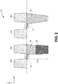
- FIG. 2 illustrates a legacy implementation of a VCG and a via trench contact (VCT).
- Legacy integrated circuit structure 200 includes a legacy implementation of legacy electrical contact structures 232, 238, respectively, with a M0 230b, 230d.
- the electrical contact structure 232 may come into contact with a trench contact below (not shown), and also be in electrical contact with M0 230b.
- the legacy electrical contact structure 232 may include two via structures, a trench connector 236 and a VCT 234 placed on top of the trench connector 236. As shown, each of these were created using a traditional via structure, having an outward taper from the bottom of the via 234, 236, to the top.
- this legacy implementation may result in the top of the VCT 234 being very close to the M0 230a, possibly causing a short, as shown in region 231, resulting in electrical contact between the VCT 234 and the M0 230a. This is particularly true given the edge placement error (EPE) during manufacture, particularly with respect to manufacturing integrated circuits with a higher density of transistors.
- EPE edge placement error
- the VCG 238 may be a single via with a traditional via structure, having an outward taper from the bottom of the VCG 238 via to the top.
- the top of the VCG 238 may be very broad due to its high aspect ratio, and be very close to the M0 230c, possibly causing a short, as shown in region 237. Again, this is particularly true given EPE during manufacture, particularly with respect to manufacturing integrated circuits with a higher density of transistors.
- FIG. 3 illustrates a cross-section of an IC structure parallel to a gate that shows the VCG with two separate sections, in accordance with various embodiments.
- IC structure 300 which may be similar to IC structure 100, includes a cross-section of a portion of a transistor that includes a gate 302, VCG 315, a VCx 320, and a M0 326, which may be similar to gate 102, VCG 115, VCX 120, and M0 126 of FIG. 1 .
- a top portion of the VCG 315 is coupled with a bottom portion of the VCx 320, where a bottom of the VCG 315 that is coupled with the gate 302 may have a larger surface area than a bottom of the VCX 320 that is coupled with the top of the VCG 315.
- the sides of the VCG 315 tapers outward from the bottom to the top. In this way, the bottom of the VCG 315 provides a good electrical connection with the gate 302, and even permits a partial overlap with a gate cut 303, that may be used to electrically and physically decouple portions of the gate 302, 305.
- FIG. 4 illustrates a top down view of an IC structure that shows a VCG that has two separate sections near a gate cut, in accordance with various embodiments.
- IC structure 400 which may be similar to IC structure 300 of FIG. 3 , shows a top-down view with the M0 326 not shown for clarity.
- VCG 415 is electrically physically coupled to the top of gate 402, with the VCx 420 electrically and physically coupled to the top of the VCG 415.
- the VCG 415 may be elongated parallel to the gate 402 to maximize contact area with the gate 402.
- the elongation of the VCG 415 may overlap in part with a gate cut 403, which may be similar to gate cut 303 of FIG. 3 .
- VCx 420 which may be physically and electrically coupled to the top of the VCG 415 may have a smaller top, to create an electrical connection with the M0 326 that may not overlap with a surface of the M0 326, therefore creating a robust connection that is more tolerant of EPE with the M0 326 during manufacture.
- FIGs. 5A-5N illustrates stages in the manufacture of an IC structure with a VCG with two separate sections, in accordance with various embodiments. These various stages of manufacture may be used to construct one or more of the features described with respect to FIGs. 1 and 3-4 .
- FIG. 5A shows an initial layer onto which the VCG 315 and the VCx 320 are to be subsequently built.
- the layer includes a FinFET 540, which may be similar to FinFET 110 of FIG. 1 , which may include a contact etch stop layer (CESL) 542, with one or more replacement metal gates (RMG) 544, 546, 548.
- the RMG 544, 546, 548 may be surrounded by a gate dielectric 545 and a gate spacer 547.
- Between the RMG 544, 546, 548 includes one or more trench connectors 550, 552, 554 that may be electrically and physically coupled with the FinFET 540.
- a pre-metal dielectric (PMD) 556 may be disposed on top of the CESL 542 and/or FinFET 540.
- PMD pre-metal dielectric
- FIG. 5B shows the structure of FIG. 5A , with an etch stop layer (ESL) 558 deposited on top of the PMD 556, the RMG 544, 546, 548, and trench connectors 550, 552, 554.
- ESL etch stop layer
- sacrificial materials are deposited and patterned as pillars 560, 562, 564, in order to get opposite slope of the portions of connectors between the gate 102 and the M0 126 of FIG. 1 .
- a pillar 560 may include an amorphous silicon (a-Si), component 560a and a silicon nitride component 560b.
- a-Si amorphous silicon
- the sacrificial pillars 560, 562, 564 are structured with an inward taper from a bottom of the pillar where they couple with the ESL 558 above the trench connectors 550, 552, 554, toward the top of the pillar.
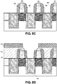
- FIG. 5C shows the structure of FIG. 5B , where a layer of silicon nitride 566 is placed around the sides of the pillars 560, 562, 564.
- FIG. 5D shows the structure of FIG. 5C , where a flowable dielectric 570 is deposited over the pillars 560, 562, 564, and subsequently planarized.
- a CHM layer 572 may then be deposited over the planar surface, and a self-aligned VCG may be etched selectively to the ESL 558 over the RMG 546.
- the etch may be selective to silicon nitride.
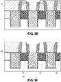
- FIG. 5E shows the structure of FIG. 5D , where the CHN layer 572 and a portion of the flowable dielectric 570 has been removed to leave flowable dielectric 571.
- this removal may be performed by using an oxide etchback.
- FIG. 5F shows the structure of FIG. 5E , but with removal of pillars 560, 562, 564, as well as removal of the ESL 558 layer above the trench connector 550, trench connector 552, and trench connector 554, as well as the ESL 558 layer above RMG 546.
- FIG. 5G shows the structure of FIG. 5F , with the metallization layer 574 applied.
- FIG. 5H shows the structure of FIG. 5G , with the surface planarized, exposing trench connectors 514, 516, 518, which may be similar to trench connectors 114, 116 of FIG. 1 , and exposing a VCG 515, which may be similar to VCG 115 of FIG. 1 , VCG 315 of FIG. 3 , or VCG 415 of FIG. 4 .
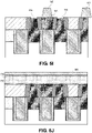
- FIG. 51 shows the structure of FIG. 5H , with VCx 520 formed on top of the VCG 515, and a VCx 521 formed on top of another trench connector.
- the VCG 515, 521 may be formed by metal deposition and a subtractive etch, or it may be formed using a replacement via technique.
- the subtractive etch may cause an over-etch of the exposed trench channel 514, 516, or of any exposed VCG 515.
- FIG. 5J shows the structure of FIG. 5H , and includes techniques for creating a VCx pillar using stack deposition techniques. This technique may be preferred for multi-via mask patterning, given the limitations of subtractively etching multiple times. In embodiments, a pattern is first collected as holes within a collection layer, and then tone inverted. This toning inversion allows a replacement contact via process with a few additional steps. A second layer of ESL layer 576 may be deposited, and subsequently an a-Si 578 layer is deposited on the ESL layer 576. A silicon nitride layer 580 is deposited on the a-Si 578 layer.
- FIG. 5K shows the structure of FIG. 5J , with part of the a-Si layer 578 and silicon nitride layer 580 etched away to leave two pillars 582, 584.
- FIG. 5L shows the structure of FIG. 5K , with a PMD layer 586 placed on top of the structure and a CMP process applied to polish the PMD layer 586 to the top surfaces of the pillars 582, 584.
- FIG. 5M shows the structure of FIG. 5L , with pillars 582, 584 removed, as well as portions of the ESL 576 at the bottom of pillars 582, 584 removed as well.
- FIG. 5N shows the structure of FIG. 5M , with a metallization layer applied and subsequently polished to provide VCx 520, which may be similar to VCx 120 of FIG. 1 , VCx 320 of FIG. 3 , and VCx 420 of FIG. 4 .
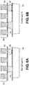
- FIGs. 6A-6B illustrate two cross-sections of an integrated circuit (IC) structure with a via between two metal lines, in accordance with various embodiments.
- FIG. 6A shows a single damascene metal line 688, which may also be referred to as a Mx+1 line, above an ESL 690 that is coupled with multiple Vx vias 692 that are in turn coupled with another metal layer 694, which may be referred to as Mx.
- Vx vias 692 may be constructed with techniques described herein, wherein the sides of the Vx vias 692 taper outward from a bottom of the Vx vias 692 to the top of the Vx vias 692.
- FIG. 6B shows an alternative embodiment, with a single damascene metal line 688, which may also be referred to as a Mx+1 line, above an ESL 690 that is coupled with multiple Vx vias 696 that are in turn coupled with another metal layer 694, which may be referred to as Mx.
- the Vx vias 696 may be constructed with techniques described herein, wherein the sides of the Vx vias 696 taper inward from a bottom of the Vx vias 696 to the top of the Vx vias 696.
- FIG. 7 illustrates an example process for manufacturing an IC structure with a VCG that has two separate sections, in accordance with various embodiments.
- process 700 may be implemented using the processes, techniques, systems, and apparatus described herein with respect to FIGs. 1 and 3-6B .
- the process may include forming a first layer of on top of a trench connector and a gate structure, with a first trench connector at a first side of the gate structure and a second trench connector at a second side of the gate structure opposite the first side of the gate structure, the gate structure including a gate and a dielectric material, wherein the first layer includes a first conductive via having a bottom side and a top side opposite the bottom side, wherein the bottom side is electrically coupled with the gate structure, and wherein the first conductive via has outwardly tapered walls extending from the bottom side of the first conductive via to the top side of the first conductive via.
- the process may further include forming a second layer on top of the first layer, wherein the second layer includes a second conductive via having a bottom side and a top side opposite the bottom side, wherein the bottom side of the second conductive via is electrically coupled with the top side of the first conductive via, and wherein the second conductive via has a inwardly tapered walls extending from the bottom side of the second conductive via to the top side of the second conductive via.
- Implementations of embodiments of the invention may be formed or carried out on a substrate, such as a semiconductor substrate.
- the semiconductor substrate may be a crystalline substrate formed using a bulk silicon or a silicon-on-insulator substructure.
- the semiconductor substrate may be formed using alternate materials, which may or may not be combined with silicon, that include but are not limited to germanium, indium antimonide, lead telluride, indium arsenide, indium phosphide, gallium arsenide, indium gallium arsenide, gallium antimonide, or other combinations of group III-V or group IV materials.
- germanium, indium antimonide, lead telluride, indium arsenide, indium phosphide, gallium arsenide, indium gallium arsenide, gallium antimonide, or other combinations of group III-V or group IV materials Although a few examples of materials from which the substrate may be formed are described here, any material that may serve as a foundation upon which a semiconductor device may be built falls within the spirit
- MOSFET metal-oxide-semiconductor field-effect transistors
- the MOS transistors may be planar transistors, nonplanar transistors, or a combination of both.
- Nonplanar transistors include FinFET transistors such as double-gate transistors and tri-gate transistors, and wrap-around or all-around gate transistors such as nanoribbon and nanowire transistors.
- Each MOS transistor includes a gate stack formed of at least two layers, a gate dielectric layer and a gate electrode layer.
- the gate dielectric layer may include one layer or a stack of layers.
- the one or more layers may include silicon oxide, silicon dioxide (SiO 2 ) and/or a high-k dielectric material.
- the high-k dielectric material may include elements such as hafnium, silicon, oxygen, titanium, tantalum, lanthanum, aluminum, zirconium, barium, strontium, yttrium, lead, scandium, niobium, and zinc.
- high-k materials that may be used in the gate dielectric layer include, but are not limited to, hafnium oxide, hafnium silicon oxide, lanthanum oxide, lanthanum aluminum oxide, zirconium oxide, zirconium silicon oxide, tantalum oxide, titanium oxide, barium strontium titanium oxide, barium titanium oxide, strontium titanium oxide, yttrium oxide, aluminum oxide, lead scandium tantalum oxide, and lead zinc niobate.
- an annealing process may be carried out on the gate dielectric layer to improve its quality when a high-k material is used.
- the gate electrode layer is formed on the gate dielectric layer and may consist of at least one P-type workfunction metal or N-type workfunction metal, depending on whether the transistor is to be a PMOS or an NMOS transistor.
- the gate electrode layer may consist of a stack of two or more metal layers, where one or more metal layers are workfunction metal layers and at least one metal layer is a fill metal layer.
- metals that may be used for the gate electrode include, but are not limited to, ruthenium, palladium, platinum, cobalt, nickel, and conductive metal oxides, e.g., ruthenium oxide.
- a P-type metal layer will enable the formation of a PMOS gate electrode with a workfunction that is between about 4.9 eV and about 5.2 eV.
- metals that may be used for the gate electrode include, but are not limited to, hafnium, zirconium, titanium, tantalum, aluminum, alloys of these metals, and carbides of these metals such as hafnium carbide, zirconium carbide, titanium carbide, tantalum carbide, and aluminum carbide.
- An N-type metal layer will enable the formation of an NMOS gate electrode with a workfunction that is between about 3.9 eV and about 4.2 eV.
- the gate electrode may consist of a "U"-shaped structure that includes a bottom portion substantially parallel to the surface of the substrate and two sidewall portions that are substantially perpendicular to the top surface of the substrate.
- at least one of the metal layers that form the gate electrode may simply be a planar layer that is substantially parallel to the top surface of the substrate and does not include sidewall portions substantially perpendicular to the top surface of the substrate.
- the gate electrode may consist of a combination of U-shaped structures and planar, non-U-shaped structures.
- the gate electrode may consist of one or more U-shaped metal layers formed atop one or more planar, non-U-shaped layers.
- a pair of sidewall spacers may be formed on opposing sides of the gate stack that bracket the gate stack.
- the sidewall spacers may be formed from a material such as silicon nitride, silicon oxide, silicon carbide, silicon nitride doped with carbon, and silicon oxynitride. Processes for forming sidewall spacers are well known in the art and generally include deposition and etching process steps. In an alternate implementation, a plurality of spacer pairs may be used, for instance, two pairs, three pairs, or four pairs of sidewall spacers may be formed on opposing sides of the gate stack.
- source and drain regions are formed within the substrate adjacent to the gate stack of each MOS transistor.
- the source and drain regions are generally formed using either an implantation/diffusion process or an etching/deposition process.
- dopants such as boron, aluminum, antimony, phosphorous, or arsenic may be ion-implanted into the substrate to form the source and drain regions.
- An annealing process that activates the dopants and causes them to diffuse further into the substrate typically follows the ion implantation process.
- the substrate may first be etched to form recesses at the locations of the source and drain regions.
- the source and drain regions may be fabricated using a silicon alloy such as silicon germanium or silicon carbide.
- the epitaxially deposited silicon alloy may be doped in situ with dopants such as boron, arsenic, or phosphorous.
- the source and drain regions may be formed using one or more alternate semiconductor materials such as germanium or a group III-V material or alloy. And in further embodiments, one or more layers of metal and/or metal alloys may be used to form the source and drain regions.
- ILD interlayer dielectrics
- the ILD layers may be formed using dielectric materials known for their applicability in integrated circuit structures, such as low-k dielectric materials. Examples of dielectric materials that may be used include, but are not limited to, silicon dioxide (SiO 2 ), carbon doped oxide (CDO), silicon nitride, organic polymers such as perfluorocyclobutane or polytetrafluoroethylene, fluorosilicate glass (FSG), and organosilicates such as silsesquioxane, siloxane, or organosilicate glass.
- the ILD layers may include pores or air gaps to further reduce their dielectric constant.
- FIG. 8 illustrates a computing device 800 in accordance with one implementation of the invention.
- the computing device 800 houses a board 802.
- the board 802 may include a number of components, including but not limited to a processor 804 and at least one communication chip 806.
- the processor 804 is physically and electrically coupled to the board 802.
- the at least one communication chip 806 is also physically and electrically coupled to the board 802.
- the communication chip 806 is part of the processor 804.
- computing device 800 may include other components that may or may not be physically and electrically coupled to the board 802. These other components include, but are not limited to, volatile memory (e.g., DRAM), non-volatile memory (e.g., ROM), flash memory, a graphics processor, a digital signal processor, a crypto processor, a chipset, an antenna, a display, a touchscreen display, a touchscreen controller, a battery, an audio codec, a video codec, a power amplifier, a global positioning system (GPS) device, a compass, an accelerometer, a gyroscope, a speaker, a camera, and a mass storage device (such as hard disk drive, compact disk (CD), digital versatile disk (DVD), and so forth).
- volatile memory e.g., DRAM
- non-volatile memory e.g., ROM
- flash memory e.g., a graphics processor, a digital signal processor, a crypto processor, a chipset, an antenna, a
- the communication chip 806 enables wireless communications for the transfer of data to and from the computing device 800.
- wireless and its derivatives may be used to describe circuits, devices, systems, methods, techniques, communications channels, etc., that may communicate data through the use of modulated electromagnetic radiation through a non-solid medium. The term does not imply that the associated devices do not contain any wires, although in some embodiments they might not.
- the communication chip 806 may implement any of a number of wireless standards or protocols, including but not limited to Wi-Fi (IEEE 802.11 family), WiMAX (IEEE 802.16 family), IEEE 802.20, long term evolution (LTE), Ev-DO, HSPA+, HSDPA+, HSUPA+, EDGE, GSM, GPRS, CDMA, TDMA, DECT, Bluetooth, derivatives thereof, as well as any other wireless protocols that are designated as 3G, 4G, 5G, and beyond.
- the computing device 800 may include a plurality of communication chips 806.
- a first communication chip 806 may be dedicated to shorter range wireless communications such as Wi-Fi and Bluetooth and a second communication chip 806 may be dedicated to longer range wireless communications such as GPS, EDGE, GPRS, CDMA, WiMAX, LTE, Ev-DO, and others.
- the processor 804 of the computing device 800 includes an integrated circuit die packaged within the processor 804.
- the integrated circuit die of the processor includes one or more devices, such as MOS-FET transistors built in accordance with implementations of the invention.
- the term "processor" may refer to any device or portion of a device that processes electronic data from registers and/or memory to transform that electronic data into other electronic data that may be stored in registers and/or memory.
- the communication chip 806 also includes an integrated circuit die packaged within the communication chip 806.
- the integrated circuit die of the communication chip includes one or more devices, such as MOS-FET transistors built in accordance with implementations of the invention.
- another component housed within the computing device 800 may contain an integrated circuit die that includes one or more devices, such as MOS-FET transistors built in accordance with implementations of the invention.
- the computing device 800 may be a laptop, a netbook, a notebook, an ultrabook, a smartphone, a tablet, a personal digital assistant (PDA), an ultra mobile PC, a mobile phone, a desktop computer, a server, a printer, a scanner, a monitor, a set-top box, an entertainment control unit, a digital camera, a portable music player, or a digital video recorder.
- the computing device 800 may be any other electronic device that processes data.
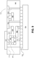
- FIG. 9 illustrates an interposer 900 that includes one or more embodiments of the invention.
- the interposer 900 is an intervening substrate used to bridge a first substrate 902 to a second substrate 904.
- the first substrate 902 may be, for instance, an integrated circuit die.
- the second substrate 904 may be, for instance, a memory module, a computer motherboard, or another integrated circuit die.
- the purpose of an interposer 900 is to spread a connection to a wider pitch or to reroute a connection to a different connection.
- an interposer 900 may couple an integrated circuit die to a ball grid array (BGA) 906 that can subsequently be coupled to the second substrate 904.
- BGA ball grid array
- first and second substrates 902/904 are attached to opposing sides of the interposer 900. In other embodiments, the first and second substrates 902/904 are attached to the same side of the interposer 900. And in further embodiments, three or more substrates are interconnected by way of the interposer 900.
- the interposer 900 may be formed of an epoxy resin, a fiberglass-reinforced epoxy resin, a ceramic material, or a polymer material such as polyimide. In further implementations, the interposer 900 may be formed of alternate rigid or flexible materials that may include the same materials described above for use in a semiconductor substrate, such as silicon, germanium, and other group III-V and group IV materials.
- the interposer 900 may include metal interconnects 908 and vias 910, including but not limited to through-silicon vias (TSVs) 912.
- the interposer 900 may further include embedded devices 914, including both passive and active devices.
- Such devices include, but are not limited to, capacitors, decoupling capacitors, resistors, inductors, fuses, diodes, transformers, sensors, and electrostatic discharge (ESD) devices. More complex devices such as radio-frequency (RF) devices, power amplifiers, power management devices, antennas, arrays, sensors, and MEMS devices may also be formed on the interposer 900.
- RF radio-frequency
- apparatuses or processes disclosed herein may be used in the fabrication of interposer 900.
- Example 1 is an integrated circuit structure, comprising: a gate structure above a channel structure, the gate structure comprising a gate and a gate dielectric; a first conductive via having a bottom side and a top side opposite the bottom side, the bottom side of the first conductive via electrically coupled with the gate, the first conductive via having outwardly tapered walls extending from the bottom side of the first conductive via to the top side of the first conductive via; a second conductive via having a bottom side and a top side opposite the bottom side, the bottom side of the second conductive via electrically coupled with the top side of the first conductive via, the second conductive via having inwardly tapered walls from the bottom side of the second conductive via to the top side of the second conductive via.
- Example 2 includes the integrated circuit structure of example 1, wherein the walls of the first conductive via have a slope between 90° and 85°, and wherein the walls of the second conductive via have a slope between 90° and 95°.
- Example 3 includes the integrated circuit structure of example 1, further comprising a metallization layer electrically coupled with the top side of the second conductive via.
- Example 4 includes the integrated circuit structure of example 1, further comprising a barrier liner between the bottom side of the second conductive via and the top side of the first conductive via.
- Example 5 includes the integrated circuit structure of example 1, wherein the bottom side of the first conductive via overlaps with a cut in the gate.
- Example 6 includes the integrated circuit structure of anyone of examples 1-5, wherein the first metal via and the second metal via include copper.
- Example 7 is an integrated circuit structure, comprising: a trench connector above a source or drain structure, the trench connector comprising a conductive metal; a first conductive via having a bottom side and a top side opposite the bottom side, the bottom side of the first conductive via electrically coupled with the trench connector, the first conductive via having outwardly tapered walls extending from the bottom side of the first conductive via to the top side of the first conductive via; a second conductive via having a bottom side and a top side opposite the bottom side, the bottom side of the second conductive via electrically coupled with the top side of the first conductive via, the second conductive via having inwardly tapered walls from the bottom side of the second conductive via to the top side of the second conductive via; a third conductive via having a first side and a second side opposite the first side, the bottom side of the third conductive via electrically coupled with gate structure above a channel structure, the gate structure comprising a gate and a gate dielectric; wherein the third conductive via has outwardly tapered
- Example 8 includes the integrated circuit structure of example 7, wherein the top side of the second conductive via is electrically coupled with a metallization layer.
- Example 9 includes the integrated circuit structure of example 7, wherein the third conductive via is electrically coupled with the metallization layer.
- Example 10 includes the integrated circuit structure of example 7, wherein the walls of the first conductive via have a slope between 90° and 85° and wherein the walls of the second conductive via have a slope between 90° and 95°.
- Example 11 includes the integrated circuit structure of any one of example 7-10, wherein the first conductive via, the second conductive via, and the third conductive via include copper.
- Example 12 is a method, comprising: forming a first layer of on top of a trench connector and a gate structure, with a first trench connector at a first side of the gate structure and a second trench connector at a second side of the gate structure opposite the first side of the gate structure, the gate structure including a gate and a dielectric material, wherein the first layer includes a first conductive via having a bottom side and a top side opposite the bottom side, wherein the bottom side is electrically coupled with the gate structure, wherein the first conductive via has outwardly tapered walls extending from the bottom side of the first conductive via to the top side of the first conductive via; and forming a second layer on top of the first layer, wherein the second layer includes a second conductive via having a bottom side and a top side opposite the bottom side, wherein the bottom side of the second conductive via is electrically coupled with the top side of the first conductive via, wherein the second conductive via has a inwardly tapered walls extending from the bottom side of the second
- Example 13 includes the method of example 12, wherein forming the first layer on top of the trench connector and the gate structure further includes forming a first pillar on top of the first trench connector and forming a second pillar on top of the second trench connector, the first pillar and the second pillar having, respectively, a bottom side and a top side opposite the bottom side, wherein the walls of the first pillar and the second pillar are inwardly tapered from the bottom side to the top side.
- Example 14 includes the method of example 13, wherein forming the first layer on top of the trench connector and the gate structure further includes applying a spacer to the walls of the first pillar and the second pillar.
- Example 15 includes the method of example 14, wherein forming the first layer on top of the trench connector and the gate structure further includes: applying a layer of pre-metal dielectric (PMD) covering the first pillar and the second pillar; and etching a volume of the PMD above the gate and between the first pillar and the second pillar, wherein the volume is bounded by a surface of the gate and the spacer covering the walls of the first pillar and the spacer covering the walls of the second pillar.
- PMD pre-metal dielectric
- Example 16 includes the method of example 15, wherein forming the first layer on top of the trench connector and the gate structure further includes removing the first pillar and the second pillar.
- Example 17 includes the method of example 16, wherein forming the first layer on top of the trench connector and the gate structure further includes depositing a metal layer in contact with the surface of the gate, the top of the first trench connector, and the top of the second trench connector.
- Example 18 includes the method of example 17, wherein forming the first layer on top of the trench connector and the gate structure further includes exposing the first trench connector, the second trench connector, and the first conductive via by planarizing the deposited metal layer.
- Example 19 includes the method of any one of examples 12-18, wherein forming the second layer on top of the first layer further includes forming the second conductive via on a top surface of the first conductive via.
- Example 20 includes the method of example 19, wherein forming the second conductive via further includes performing a metal direct etch.
Landscapes
- Internal Circuitry In Semiconductor Integrated Circuit Devices (AREA)
- Engineering & Computer Science (AREA)
- Manufacturing & Machinery (AREA)
- Metal-Oxide And Bipolar Metal-Oxide Semiconductor Integrated Circuits (AREA)
Abstract
Description
- Embodiments of the present disclosure generally relate to the field of integrated circuit (IC) manufacturing, and in particular to gate structure contacts.
- Continued growth in computing devices, virtual machines and cloud computing will continue to increase the demand for increased density of transistors in an IC.
-
-
FIG. 1 illustrates a cross-section of an integrated circuit (IC) structure perpendicular to a gate that shows a via gate contact (VCG) that has two separate sections, in accordance with various embodiments. -
FIG. 2 illustrates a legacy implementation of a VCG and a via trench contact (VCT). -
FIG. 3 illustrates a cross-section of an IC structure parallel to a gate that shows the VCG with two separate sections, in accordance with various embodiments. -
FIG. 4 illustrates a top down view of an IC structure that shows a VCG that has two separate sections near a gate cut, in accordance with various embodiments. -
FIGs. 5A-5N illustrates stages in the manufacture of an IC structure with a VCG with two separate sections, in accordance with various embodiments. -
FIGs. 6A-6B illustrate two cross-sections of an integrated circuit (IC) structure with a via between two metal lines, in accordance with various embodiments. -
FIG. 7 illustrates an example process for manufacturing a IC structure with a VCG that has two separate sections, in accordance with various embodiments. -
FIG. 8 illustrates acomputing device 800 in accordance with one implementation of the invention. -
FIG. 9 illustrates aninterposer 900 that includes one or more embodiments of the invention. - Embodiments described herein may be related to apparatuses, processes, and techniques used to construct via gate contact (VCG) between a metal gate of a gate structure and a metallization layer, which may be referred to as M0. In embodiments, the VCG is split into two separate portions. The bottom portion, VCG, may be oversized with respect to the metal gate and may be self-aligned to a trench connector that is in a same layer as the bottom portion of the VCG. The top portion, which may be referred to as VCx, may be an inverse taper that may be used to electrically couple the bottom portion VCG, or electrically couple another trench contact, with the metallization layer.
- Legacy implementations, as discussed further below with respect to
FIG. 2 , have a low process margin which can result in higher rates of via short and/or open failures when increasing transistor density is attempted. In particular, a VCG that is constructed using legacy techniques, such as two stacked vias or as a single via, requires a greater distance between the M0 layers because of the increasing widening from the base of the VCG to the top of the VCG where it electrically couples with the M0 layer. This increases the possibility of shorting. - In particular with legacy implementations, as the M0 pitch scales down, it becomes more difficult to align a VCG and a via trench contact (VCT) to the M0. This problem is particularly difficult with a subtractive M0, where there is no higher-k dielectric to prevent time-dependent dielectric breakdown. A concurrent issue in legacy implementations is that in standard cells, the M0-to-VCG-to-gate connections becomes very tight, often leaving zero to negative VCG-to-gate enclosure which results in high risk of a contact open.
- A result of embodiments described herein that provide the bottom VCG with a large area, and the top VCx with a small top area allows standard cells to be scaled further by (1) fully contacting the gate, and (2) by increasing the margin in the contact with M0 to allow for edge placement error (EPE) during manufacturing. In particular, when M0 itself has an inverse taper due to subtractive metal formation during manufacture. This will allow for improved quality and increased density of transistors on an IC. In addition, embodiments of processes described herein allow the VCG to self-align to the gate contact during manufacture.
- In the following detailed description, reference is made to the accompanying drawings which form a part hereof, wherein like numerals designate like parts throughout, and in which is shown by way of illustration embodiments in which the subject matter of the present disclosure may be practiced. It is to be understood that other embodiments may be utilized and structural or logical changes may be made without departing from the scope of the present disclosure. Therefore, the following detailed description is not to be taken in a limiting sense, and the scope of embodiments is defined by the appended claims and their equivalents.
- For the purposes of the present disclosure, the phrase "A and/or B" means (A), (B), or (A and B). For the purposes of the present disclosure, the phrase "A, B, and/or C" means (A), (B), (C), (A and B), (A and C), (B and C), or (A, B and C).
- The description may use perspective-based descriptions such as top/bottom, in/out, over/under, and the like. Such descriptions are merely used to facilitate the discussion and are not intended to restrict the application of embodiments described herein to any particular orientation.
- The description may use the phrases "in an embodiment," or "in embodiments," which may each refer to one or more of the same or different embodiments. Furthermore, the terms "comprising," "including," "having," and the like, as used with respect to embodiments of the present disclosure, are synonymous.
- The term "coupled with," along with its derivatives, may be used herein. "Coupled" may mean one or more of the following. "Coupled" may mean that two or more elements are in direct physical or electrical contact. However, "coupled" may also mean that two or more elements indirectly contact each other, but yet still cooperate or interact with each other, and may mean that one or more other elements are coupled or connected between the elements that are said to be coupled with each other. The term "directly coupled" may mean that two or more elements are in direct contact.
- Various operations may be described as multiple discrete operations in turn, in a manner that is most helpful in understanding the claimed subject matter. However, the order of description should not be construed as to imply that these operations are necessarily order dependent.
- As used herein, the term "module" may refer to, be part of, or include an ASIC, an electronic circuit, a processor (shared, dedicated, or group) and/or memory (shared, dedicated, or group) that execute one or more software or firmware programs, a combinational logic circuit, and/or other suitable components that provide the described functionality.
- Various Figures herein may depict one or more layers of one or more package assemblies. The layers depicted herein are depicted as examples of relative positions of the layers of the different package assemblies. The layers are depicted for the purposes of explanation, and are not drawn to scale. Therefore, comparative sizes of layers should not be assumed from the Figures, and sizes, thicknesses, or dimensions may be assumed for some embodiments only where specifically indicated or discussed.
- Various embodiments may include any suitable combination of the above-described embodiments including alternative (or) embodiments of embodiments that are described in conjunctive form (and) above (e.g., the "and" may be "and/or"). Furthermore, some embodiments may include one or more articles of manufacture (e.g., non-transitory computer-readable media) having instructions, stored thereon, that when executed result in actions of any of the above-described embodiments. Moreover, some embodiments may include apparatuses or systems having any suitable means for carrying out the various operations of the above-described embodiments.
-
FIG. 1 illustrates a cross-section of an integrated circuit (IC) structure perpendicular to a gate that shows a via gate contact (VCG) that has two separate sections, in accordance with various embodiments.IC structure 100 includes a cross-section of a portion of a transistor that includes agate 102 that is surrounded by a gate dielectric 104.Trench connectors spacers trench connectors gate 102 andtrench connectors structure 110. - Within
layer 112 there may be aVCG 115 that is electrically and physically coupled to thegate 102.Layer 112 may also includetrench connectors trench connector layer 112 may include a dielectric 118, which may serve as a spacer for VCG 115 self-alignment during manufacture. In embodiments, thetrench connectors trench connectors trench connectors trench connectors trench connectors - In embodiments, the VCG 115 may have an outward taper from the VCG 115 bottom where it couples with the
gate 102, to the top of the VCG 115. TheVCx 120 may be coupled with the metal 0 layer (M0) 126. At either side of the VCx there may be an inversetaper trench connector trench connector trench connector trench connector M0 126. - In embodiments, the dielectric 118 within
layer 112 may have various cavities formed into which thetrench connectors VCG 115 may be formed. A geometry of the various cavities will produce respective geometries (e.g. tapers) in thetrench connectors VCG 115. These various cavities within the dielectric 118 may be used to self-align theVCG 115 with thetrench connectors gate 102. -
FIG. 2 illustrates a legacy implementation of a VCG and a via trench contact (VCT). Legacy integratedcircuit structure 200 includes a legacy implementation of legacyelectrical contact structures M0 electrical contact structure 232 may come into contact with a trench contact below (not shown), and also be in electrical contact withM0 230b. During legacy manufacture techniques, the legacyelectrical contact structure 232 may include two via structures, atrench connector 236 and aVCT 234 placed on top of thetrench connector 236. As shown, each of these were created using a traditional via structure, having an outward taper from the bottom of the via 234, 236, to the top. - Because of the upward taper, this legacy implementation may result in the top of the
VCT 234 being very close to theM0 230a, possibly causing a short, as shown inregion 231, resulting in electrical contact between theVCT 234 and theM0 230a. This is particularly true given the edge placement error (EPE) during manufacture, particularly with respect to manufacturing integrated circuits with a higher density of transistors. - In legacy implementations, the
VCG 238 may be a single via with a traditional via structure, having an outward taper from the bottom of theVCG 238 via to the top. In this implementation, because of the height of the via, the top of theVCG 238 may be very broad due to its high aspect ratio, and be very close to theM0 230c, possibly causing a short, as shown inregion 237. Again, this is particularly true given EPE during manufacture, particularly with respect to manufacturing integrated circuits with a higher density of transistors. -
FIG. 3 illustrates a cross-section of an IC structure parallel to a gate that shows the VCG with two separate sections, in accordance with various embodiments.IC structure 300, which may be similar toIC structure 100, includes a cross-section of a portion of a transistor that includes agate 302,VCG 315, aVCx 320, and aM0 326, which may be similar togate 102,VCG 115,VCX 120, andM0 126 ofFIG. 1 . - As shown, a top portion of the
VCG 315 is coupled with a bottom portion of theVCx 320, where a bottom of theVCG 315 that is coupled with thegate 302 may have a larger surface area than a bottom of theVCX 320 that is coupled with the top of theVCG 315. The sides of theVCG 315 tapers outward from the bottom to the top. In this way, the bottom of theVCG 315 provides a good electrical connection with thegate 302, and even permits a partial overlap with agate cut 303, that may be used to electrically and physically decouple portions of thegate -
FIG. 4 illustrates a top down view of an IC structure that shows a VCG that has two separate sections near a gate cut, in accordance with various embodiments.IC structure 400, which may be similar toIC structure 300 ofFIG. 3 , shows a top-down view with theM0 326 not shown for clarity.VCG 415 is electrically physically coupled to the top ofgate 402, with theVCx 420 electrically and physically coupled to the top of theVCG 415. - In embodiments, the
VCG 415 may be elongated parallel to thegate 402 to maximize contact area with thegate 402. In embodiments, the elongation of theVCG 415 may overlap in part with agate cut 403, which may be similar to gate cut 303 ofFIG. 3 . In this way, even if there isgate cut 403 overlap, the electrical connection between theVCG 415 and thegate 402 will be a robust connection.VCx 420, which may be physically and electrically coupled to the top of theVCG 415 may have a smaller top, to create an electrical connection with theM0 326 that may not overlap with a surface of theM0 326, therefore creating a robust connection that is more tolerant of EPE with theM0 326 during manufacture. -
FIGs. 5A-5N illustrates stages in the manufacture of an IC structure with a VCG with two separate sections, in accordance with various embodiments. These various stages of manufacture may be used to construct one or more of the features described with respect toFIGs. 1 and3-4 . -
FIG. 5A shows an initial layer onto which theVCG 315 and theVCx 320 are to be subsequently built. The layer includes aFinFET 540, which may be similar toFinFET 110 ofFIG. 1 , which may include a contact etch stop layer (CESL) 542, with one or more replacement metal gates (RMG) 544, 546, 548. In embodiments, theRMG gate dielectric 545 and agate spacer 547. Between theRMG more trench connectors FinFET 540. In addition, a pre-metal dielectric (PMD) 556 may be disposed on top of theCESL 542 and/orFinFET 540. -
FIG. 5B shows the structure ofFIG. 5A , with an etch stop layer (ESL) 558 deposited on top of thePMD 556, theRMG trench connectors etch stop layer 558, sacrificial materials are deposited and patterned aspillars gate 102 and theM0 126 ofFIG. 1 . In embodiments, apillar 560 may include an amorphous silicon (a-Si),component 560a and asilicon nitride component 560b. Note that thesacrificial pillars ESL 558 above thetrench connectors -
FIG. 5C shows the structure ofFIG. 5B , where a layer ofsilicon nitride 566 is placed around the sides of thepillars -
FIG. 5D shows the structure ofFIG. 5C , where aflowable dielectric 570 is deposited over thepillars CHM layer 572 may then be deposited over the planar surface, and a self-aligned VCG may be etched selectively to theESL 558 over theRMG 546. In embodiments, the etch may be selective to silicon nitride. -
FIG. 5E shows the structure ofFIG. 5D , where theCHN layer 572 and a portion of theflowable dielectric 570 has been removed to leaveflowable dielectric 571. In embodiments, this removal may be performed by using an oxide etchback. -
FIG. 5F shows the structure ofFIG. 5E , but with removal ofpillars ESL 558 layer above thetrench connector 550,trench connector 552, andtrench connector 554, as well as theESL 558 layer aboveRMG 546. -
FIG. 5G shows the structure ofFIG. 5F , with themetallization layer 574 applied. -
FIG. 5H shows the structure ofFIG. 5G , with the surface planarized, exposingtrench connectors trench connectors FIG. 1 , and exposing aVCG 515, which may be similar toVCG 115 ofFIG. 1 ,VCG 315 ofFIG. 3 , orVCG 415 ofFIG. 4 . -
FIG. 51 shows the structure ofFIG. 5H , withVCx 520 formed on top of theVCG 515, and aVCx 521 formed on top of another trench connector. In embodiments, theVCG trench channel VCG 515. -
FIG. 5J shows the structure ofFIG. 5H , and includes techniques for creating a VCx pillar using stack deposition techniques. This technique may be preferred for multi-via mask patterning, given the limitations of subtractively etching multiple times. In embodiments, a pattern is first collected as holes within a collection layer, and then tone inverted. This toning inversion allows a replacement contact via process with a few additional steps. A second layer ofESL layer 576 may be deposited, and subsequently an a-Si 578 layer is deposited on theESL layer 576. Asilicon nitride layer 580 is deposited on the a-Si 578 layer. -
FIG. 5K shows the structure ofFIG. 5J , with part of thea-Si layer 578 andsilicon nitride layer 580 etched away to leave twopillars -
FIG. 5L shows the structure ofFIG. 5K , with aPMD layer 586 placed on top of the structure and a CMP process applied to polish thePMD layer 586 to the top surfaces of thepillars -
FIG. 5M shows the structure ofFIG. 5L , withpillars ESL 576 at the bottom ofpillars -
FIG. 5N shows the structure ofFIG. 5M , with a metallization layer applied and subsequently polished to provideVCx 520, which may be similar toVCx 120 ofFIG. 1 ,VCx 320 ofFIG. 3 , andVCx 420 ofFIG. 4 . -
FIGs. 6A-6B illustrate two cross-sections of an integrated circuit (IC) structure with a via between two metal lines, in accordance with various embodiments. -
FIG. 6A shows a single damascene metal line 688, which may also be referred to as a Mx+1 line, above an ESL 690 that is coupled with multiple Vx vias 692 that are in turn coupled with another metal layer 694, which may be referred to as Mx. In embodiments, Vx vias 692 may be constructed with techniques described herein, wherein the sides of the Vx vias 692 taper outward from a bottom of the Vx vias 692 to the top of the Vx vias 692. -
FIG. 6B shows an alternative embodiment, with a single damascene metal line 688, which may also be referred to as a Mx+1 line, above an ESL 690 that is coupled with multiple Vx vias 696 that are in turn coupled with another metal layer 694, which may be referred to as Mx. In embodiments, the Vx vias 696 may be constructed with techniques described herein, wherein the sides of the Vx vias 696 taper inward from a bottom of the Vx vias 696 to the top of the Vx vias 696. -
FIG. 7 illustrates an example process for manufacturing an IC structure with a VCG that has two separate sections, in accordance with various embodiments. In embodiments,process 700 may be implemented using the processes, techniques, systems, and apparatus described herein with respect toFIGs. 1 and3-6B . - At
block 702, the process may include forming a first layer of on top of a trench connector and a gate structure, with a first trench connector at a first side of the gate structure and a second trench connector at a second side of the gate structure opposite the first side of the gate structure, the gate structure including a gate and a dielectric material, wherein the first layer includes a first conductive via having a bottom side and a top side opposite the bottom side, wherein the bottom side is electrically coupled with the gate structure, and wherein the first conductive via has outwardly tapered walls extending from the bottom side of the first conductive via to the top side of the first conductive via. - At
block 704, the process may further include forming a second layer on top of the first layer, wherein the second layer includes a second conductive via having a bottom side and a top side opposite the bottom side, wherein the bottom side of the second conductive via is electrically coupled with the top side of the first conductive via, and wherein the second conductive via has a inwardly tapered walls extending from the bottom side of the second conductive via to the top side of the second conductive via. - Implementations of embodiments of the invention may be formed or carried out on a substrate, such as a semiconductor substrate. In one implementation, the semiconductor substrate may be a crystalline substrate formed using a bulk silicon or a silicon-on-insulator substructure. In other implementations, the semiconductor substrate may be formed using alternate materials, which may or may not be combined with silicon, that include but are not limited to germanium, indium antimonide, lead telluride, indium arsenide, indium phosphide, gallium arsenide, indium gallium arsenide, gallium antimonide, or other combinations of group III-V or group IV materials. Although a few examples of materials from which the substrate may be formed are described here, any material that may serve as a foundation upon which a semiconductor device may be built falls within the spirit and scope of the present invention.
- A plurality of transistors, such as metal-oxide-semiconductor field-effect transistors (MOSFET or simply MOS transistors), may be fabricated on the substrate. In various implementations of the invention, the MOS transistors may be planar transistors, nonplanar transistors, or a combination of both. Nonplanar transistors include FinFET transistors such as double-gate transistors and tri-gate transistors, and wrap-around or all-around gate transistors such as nanoribbon and nanowire transistors. Although the implementations described herein may illustrate only planar transistors, it should be noted that the invention may also be carried out using nonplanar transistors.
- Each MOS transistor includes a gate stack formed of at least two layers, a gate dielectric layer and a gate electrode layer. The gate dielectric layer may include one layer or a stack of layers. The one or more layers may include silicon oxide, silicon dioxide (SiO2) and/or a high-k dielectric material. The high-k dielectric material may include elements such as hafnium, silicon, oxygen, titanium, tantalum, lanthanum, aluminum, zirconium, barium, strontium, yttrium, lead, scandium, niobium, and zinc. Examples of high-k materials that may be used in the gate dielectric layer include, but are not limited to, hafnium oxide, hafnium silicon oxide, lanthanum oxide, lanthanum aluminum oxide, zirconium oxide, zirconium silicon oxide, tantalum oxide, titanium oxide, barium strontium titanium oxide, barium titanium oxide, strontium titanium oxide, yttrium oxide, aluminum oxide, lead scandium tantalum oxide, and lead zinc niobate. In some embodiments, an annealing process may be carried out on the gate dielectric layer to improve its quality when a high-k material is used.
- The gate electrode layer is formed on the gate dielectric layer and may consist of at least one P-type workfunction metal or N-type workfunction metal, depending on whether the transistor is to be a PMOS or an NMOS transistor. In some implementations, the gate electrode layer may consist of a stack of two or more metal layers, where one or more metal layers are workfunction metal layers and at least one metal layer is a fill metal layer.
- For a PMOS transistor, metals that may be used for the gate electrode include, but are not limited to, ruthenium, palladium, platinum, cobalt, nickel, and conductive metal oxides, e.g., ruthenium oxide. A P-type metal layer will enable the formation of a PMOS gate electrode with a workfunction that is between about 4.9 eV and about 5.2 eV. For an NMOS transistor, metals that may be used for the gate electrode include, but are not limited to, hafnium, zirconium, titanium, tantalum, aluminum, alloys of these metals, and carbides of these metals such as hafnium carbide, zirconium carbide, titanium carbide, tantalum carbide, and aluminum carbide. An N-type metal layer will enable the formation of an NMOS gate electrode with a workfunction that is between about 3.9 eV and about 4.2 eV.
- In some implementations, the gate electrode may consist of a "U"-shaped structure that includes a bottom portion substantially parallel to the surface of the substrate and two sidewall portions that are substantially perpendicular to the top surface of the substrate. In another implementation, at least one of the metal layers that form the gate electrode may simply be a planar layer that is substantially parallel to the top surface of the substrate and does not include sidewall portions substantially perpendicular to the top surface of the substrate. In further implementations of the invention, the gate electrode may consist of a combination of U-shaped structures and planar, non-U-shaped structures. For example, the gate electrode may consist of one or more U-shaped metal layers formed atop one or more planar, non-U-shaped layers.
- In some implementations of the invention, a pair of sidewall spacers may be formed on opposing sides of the gate stack that bracket the gate stack. The sidewall spacers may be formed from a material such as silicon nitride, silicon oxide, silicon carbide, silicon nitride doped with carbon, and silicon oxynitride. Processes for forming sidewall spacers are well known in the art and generally include deposition and etching process steps. In an alternate implementation, a plurality of spacer pairs may be used, for instance, two pairs, three pairs, or four pairs of sidewall spacers may be formed on opposing sides of the gate stack.
- As is well known in the art, source and drain regions are formed within the substrate adjacent to the gate stack of each MOS transistor. The source and drain regions are generally formed using either an implantation/diffusion process or an etching/deposition process. In the former process, dopants such as boron, aluminum, antimony, phosphorous, or arsenic may be ion-implanted into the substrate to form the source and drain regions. An annealing process that activates the dopants and causes them to diffuse further into the substrate typically follows the ion implantation process. In the latter process, the substrate may first be etched to form recesses at the locations of the source and drain regions. An epitaxial deposition process may then be carried out to fill the recesses with material that is used to fabricate the source and drain regions. In some implementations, the source and drain regions may be fabricated using a silicon alloy such as silicon germanium or silicon carbide. In some implementations the epitaxially deposited silicon alloy may be doped in situ with dopants such as boron, arsenic, or phosphorous. In further embodiments, the source and drain regions may be formed using one or more alternate semiconductor materials such as germanium or a group III-V material or alloy. And in further embodiments, one or more layers of metal and/or metal alloys may be used to form the source and drain regions.
- One or more interlayer dielectrics (ILD) are deposited over the MOS transistors. The ILD layers may be formed using dielectric materials known for their applicability in integrated circuit structures, such as low-k dielectric materials. Examples of dielectric materials that may be used include, but are not limited to, silicon dioxide (SiO2), carbon doped oxide (CDO), silicon nitride, organic polymers such as perfluorocyclobutane or polytetrafluoroethylene, fluorosilicate glass (FSG), and organosilicates such as silsesquioxane, siloxane, or organosilicate glass. The ILD layers may include pores or air gaps to further reduce their dielectric constant.
-
FIG. 8 illustrates acomputing device 800 in accordance with one implementation of the invention. Thecomputing device 800 houses aboard 802. Theboard 802 may include a number of components, including but not limited to aprocessor 804 and at least onecommunication chip 806. Theprocessor 804 is physically and electrically coupled to theboard 802. In some implementations the at least onecommunication chip 806 is also physically and electrically coupled to theboard 802. In further implementations, thecommunication chip 806 is part of theprocessor 804. - Depending on its applications,
computing device 800 may include other components that may or may not be physically and electrically coupled to theboard 802. These other components include, but are not limited to, volatile memory (e.g., DRAM), non-volatile memory (e.g., ROM), flash memory, a graphics processor, a digital signal processor, a crypto processor, a chipset, an antenna, a display, a touchscreen display, a touchscreen controller, a battery, an audio codec, a video codec, a power amplifier, a global positioning system (GPS) device, a compass, an accelerometer, a gyroscope, a speaker, a camera, and a mass storage device (such as hard disk drive, compact disk (CD), digital versatile disk (DVD), and so forth). - The
communication chip 806 enables wireless communications for the transfer of data to and from thecomputing device 800. The term "wireless" and its derivatives may be used to describe circuits, devices, systems, methods, techniques, communications channels, etc., that may communicate data through the use of modulated electromagnetic radiation through a non-solid medium. The term does not imply that the associated devices do not contain any wires, although in some embodiments they might not. Thecommunication chip 806 may implement any of a number of wireless standards or protocols, including but not limited to Wi-Fi (IEEE 802.11 family), WiMAX (IEEE 802.16 family), IEEE 802.20, long term evolution (LTE), Ev-DO, HSPA+, HSDPA+, HSUPA+, EDGE, GSM, GPRS, CDMA, TDMA, DECT, Bluetooth, derivatives thereof, as well as any other wireless protocols that are designated as 3G, 4G, 5G, and beyond. Thecomputing device 800 may include a plurality ofcommunication chips 806. For instance, afirst communication chip 806 may be dedicated to shorter range wireless communications such as Wi-Fi and Bluetooth and asecond communication chip 806 may be dedicated to longer range wireless communications such as GPS, EDGE, GPRS, CDMA, WiMAX, LTE, Ev-DO, and others. - The
processor 804 of thecomputing device 800 includes an integrated circuit die packaged within theprocessor 804. In some implementations of the invention, the integrated circuit die of the processor includes one or more devices, such as MOS-FET transistors built in accordance with implementations of the invention. The term "processor" may refer to any device or portion of a device that processes electronic data from registers and/or memory to transform that electronic data into other electronic data that may be stored in registers and/or memory. - The
communication chip 806 also includes an integrated circuit die packaged within thecommunication chip 806. In accordance with another implementation of the invention, the integrated circuit die of the communication chip includes one or more devices, such as MOS-FET transistors built in accordance with implementations of the invention. - In further implementations, another component housed within the
computing device 800 may contain an integrated circuit die that includes one or more devices, such as MOS-FET transistors built in accordance with implementations of the invention. - In various implementations, the
computing device 800 may be a laptop, a netbook, a notebook, an ultrabook, a smartphone, a tablet, a personal digital assistant (PDA), an ultra mobile PC, a mobile phone, a desktop computer, a server, a printer, a scanner, a monitor, a set-top box, an entertainment control unit, a digital camera, a portable music player, or a digital video recorder. In further implementations, thecomputing device 800 may be any other electronic device that processes data. -
FIG. 9 illustrates aninterposer 900 that includes one or more embodiments of the invention. Theinterposer 900 is an intervening substrate used to bridge afirst substrate 902 to asecond substrate 904. Thefirst substrate 902 may be, for instance, an integrated circuit die. Thesecond substrate 904 may be, for instance, a memory module, a computer motherboard, or another integrated circuit die. Generally, the purpose of aninterposer 900 is to spread a connection to a wider pitch or to reroute a connection to a different connection. For example, aninterposer 900 may couple an integrated circuit die to a ball grid array (BGA) 906 that can subsequently be coupled to thesecond substrate 904. In some embodiments, the first andsecond substrates 902/904 are attached to opposing sides of theinterposer 900. In other embodiments, the first andsecond substrates 902/904 are attached to the same side of theinterposer 900. And in further embodiments, three or more substrates are interconnected by way of theinterposer 900. - The
interposer 900 may be formed of an epoxy resin, a fiberglass-reinforced epoxy resin, a ceramic material, or a polymer material such as polyimide. In further implementations, theinterposer 900 may be formed of alternate rigid or flexible materials that may include the same materials described above for use in a semiconductor substrate, such as silicon, germanium, and other group III-V and group IV materials. - The
interposer 900 may includemetal interconnects 908 and vias 910, including but not limited to through-silicon vias (TSVs) 912. Theinterposer 900 may further include embeddeddevices 914, including both passive and active devices. Such devices include, but are not limited to, capacitors, decoupling capacitors, resistors, inductors, fuses, diodes, transformers, sensors, and electrostatic discharge (ESD) devices. More complex devices such as radio-frequency (RF) devices, power amplifiers, power management devices, antennas, arrays, sensors, and MEMS devices may also be formed on theinterposer 900. In accordance with embodiments of the invention, apparatuses or processes disclosed herein may be used in the fabrication ofinterposer 900. - The above description of illustrated embodiments, including what is described in the Abstract, is not intended to be exhaustive or to limit embodiments to the precise forms disclosed. While specific embodiments are described herein for illustrative purposes, various equivalent modifications are possible within the scope of the embodiments, as those skilled in the relevant art will recognize.
- These modifications may be made to the embodiments in light of the above detailed description. The terms used in the following claims should not be construed to limit the embodiments to the specific implementations disclosed in the specification and the claims. Rather, the scope of the invention is to be determined entirely by the following claims, which are to be construed in accordance with established doctrines of claim interpretation.
- The following paragraphs describe examples of various embodiments.
- Example 1 is an integrated circuit structure, comprising: a gate structure above a channel structure, the gate structure comprising a gate and a gate dielectric; a first conductive via having a bottom side and a top side opposite the bottom side, the bottom side of the first conductive via electrically coupled with the gate, the first conductive via having outwardly tapered walls extending from the bottom side of the first conductive via to the top side of the first conductive via; a second conductive via having a bottom side and a top side opposite the bottom side, the bottom side of the second conductive via electrically coupled with the top side of the first conductive via, the second conductive via having inwardly tapered walls from the bottom side of the second conductive via to the top side of the second conductive via.
- Example 2 includes the integrated circuit structure of example 1, wherein the walls of the first conductive via have a slope between 90° and 85°, and wherein the walls of the second conductive via have a slope between 90° and 95°.
- Example 3 includes the integrated circuit structure of example 1, further comprising a metallization layer electrically coupled with the top side of the second conductive via.
- Example 4 includes the integrated circuit structure of example 1, further comprising a barrier liner between the bottom side of the second conductive via and the top side of the first conductive via.
- Example 5 includes the integrated circuit structure of example 1, wherein the bottom side of the first conductive via overlaps with a cut in the gate.
- Example 6 includes the integrated circuit structure of anyone of examples 1-5, wherein the first metal via and the second metal via include copper.
- Example 7 is an integrated circuit structure, comprising: a trench connector above a source or drain structure, the trench connector comprising a conductive metal; a first conductive via having a bottom side and a top side opposite the bottom side, the bottom side of the first conductive via electrically coupled with the trench connector, the first conductive via having outwardly tapered walls extending from the bottom side of the first conductive via to the top side of the first conductive via; a second conductive via having a bottom side and a top side opposite the bottom side, the bottom side of the second conductive via electrically coupled with the top side of the first conductive via, the second conductive via having inwardly tapered walls from the bottom side of the second conductive via to the top side of the second conductive via; a third conductive via having a first side and a second side opposite the first side, the bottom side of the third conductive via electrically coupled with gate structure above a channel structure, the gate structure comprising a gate and a gate dielectric; wherein the third conductive via has outwardly tapered walls extending from the bottom side of the third conductive via to the top side of the third conductive via; and wherein the first conductive via and the third conductive via are within a layer of the integrated circuit structure.
- Example 8 includes the integrated circuit structure of example 7, wherein the top side of the second conductive via is electrically coupled with a metallization layer.
- Example 9 includes the integrated circuit structure of example 7, wherein the third conductive via is electrically coupled with the metallization layer.
- Example 10 includes the integrated circuit structure of example 7, wherein the walls of the first conductive via have a slope between 90° and 85° and wherein the walls of the second conductive via have a slope between 90° and 95°.
- Example 11 includes the integrated circuit structure of any one of example 7-10, wherein the first conductive via, the second conductive via, and the third conductive via include copper.
- Example 12 is a method, comprising: forming a first layer of on top of a trench connector and a gate structure, with a first trench connector at a first side of the gate structure and a second trench connector at a second side of the gate structure opposite the first side of the gate structure, the gate structure including a gate and a dielectric material, wherein the first layer includes a first conductive via having a bottom side and a top side opposite the bottom side, wherein the bottom side is electrically coupled with the gate structure, wherein the first conductive via has outwardly tapered walls extending from the bottom side of the first conductive via to the top side of the first conductive via; and forming a second layer on top of the first layer, wherein the second layer includes a second conductive via having a bottom side and a top side opposite the bottom side, wherein the bottom side of the second conductive via is electrically coupled with the top side of the first conductive via, wherein the second conductive via has a inwardly tapered walls extending from the bottom side of the second conductive via to the top side of the second conductive via.
- Example 13 includes the method of example 12, wherein forming the first layer on top of the trench connector and the gate structure further includes forming a first pillar on top of the first trench connector and forming a second pillar on top of the second trench connector, the first pillar and the second pillar having, respectively, a bottom side and a top side opposite the bottom side, wherein the walls of the first pillar and the second pillar are inwardly tapered from the bottom side to the top side.
- Example 14 includes the method of example 13, wherein forming the first layer on top of the trench connector and the gate structure further includes applying a spacer to the walls of the first pillar and the second pillar.
- Example 15 includes the method of example 14, wherein forming the first layer on top of the trench connector and the gate structure further includes: applying a layer of pre-metal dielectric (PMD) covering the first pillar and the second pillar; and etching a volume of the PMD above the gate and between the first pillar and the second pillar, wherein the volume is bounded by a surface of the gate and the spacer covering the walls of the first pillar and the spacer covering the walls of the second pillar.
- Example 16 includes the method of example 15, wherein forming the first layer on top of the trench connector and the gate structure further includes removing the first pillar and the second pillar.
- Example 17 includes the method of example 16, wherein forming the first layer on top of the trench connector and the gate structure further includes depositing a metal layer in contact with the surface of the gate, the top of the first trench connector, and the top of the second trench connector.
- Example 18 includes the method of example 17, wherein forming the first layer on top of the trench connector and the gate structure further includes exposing the first trench connector, the second trench connector, and the first conductive via by planarizing the deposited metal layer.
- Example 19 includes the method of any one of examples 12-18, wherein forming the second layer on top of the first layer further includes forming the second conductive via on a top surface of the first conductive via.
- Example 20 includes the method of example 19, wherein forming the second conductive via further includes performing a metal direct etch.
Claims (15)
- An integrated circuit structure, comprising:a gate structure above a channel structure, the gate structure comprising a gate and a gate dielectric;a first conductive via having a bottom side and a top side opposite the bottom side,the bottom side of the first conductive via electrically coupled with the gate,the first conductive via having outwardly tapered walls extending from the bottom side of the first conductive via to the top side of the first conductive via;a second conductive via having a bottom side and a top side opposite the bottom side,the bottom side of the second conductive via electrically coupled with the top side of the first conductive via,the second conductive via having inwardly tapered walls from the bottom side of the second conductive via to the top side of the second conductive via.
- The integrated circuit structure of claim 1, wherein the walls of the first conductive via have a slope between 90° and 85°, and wherein the walls of the second conductive via have a slope between 90° and 95°.
- The integrated circuit structure of claim 1, further comprising a metallization layer electrically coupled with the top side of the second conductive via.
- The integrated circuit structure of claim 1, further comprising a barrier liner between the bottom side of the second conductive via and the top side of the first conductive via.
- The integrated circuit structure of claim 1, wherein the bottom side of the first conductive via overlaps with a cut in the gate.
- The integrated circuit structure of claim 1, 2, 3, 4 or 5, wherein the first metal via and the second metal via include copper.
- A method, comprising:forming a first layer of on top of a trench connector and a gate structure, with a first trench connector at a first side of the gate structure and a second trench connector at a second side of the gate structure opposite the first side of the gate structure, the gate structure including a gate and a dielectric material,wherein the first layer includes a first conductive via having a bottom side and a top side opposite the bottom side,wherein the bottom side is electrically coupled with the gate structure,wherein the first conductive via has outwardly tapered walls extending from the bottom side of the first conductive via to the top side of the first conductive via; andforming a second layer on top of the first layer,wherein the second layer includes a second conductive via having a bottom side and a top side opposite the bottom side,wherein the bottom side of the second conductive via is electrically coupled with the top side of the first conductive via,wherein the second conductive via has a inwardly tapered walls extending from the bottom side of the second conductive via to the top side of the second conductive via.
- The method of claim 7, wherein forming the first layer on top of the trench connector and the gate structure further includes forming a first pillar on top of the first trench connector and forming a second pillar on top of the second trench connector, the first pillar and the second pillar having, respectively, a bottom side and a top side opposite the bottom side, wherein the walls of the first pillar and the second pillar are inwardly tapered from the bottom side to the top side.
- The method of claim 8, wherein forming the first layer on top of the trench connector and the gate structure further includes applying a spacer to the walls of the first pillar and the second pillar.
- The method of claim 9, wherein forming the first layer on top of the trench connector and the gate structure further includes:applying a layer of pre-metal dielectric (PMD) covering the first pillar and the second pillar; andetching a volume of the PMD above the gate and between the first pillar and the second pillar, wherein the volume is bounded by a surface of the gate and the spacer covering the walls of the first pillar and the spacer covering the walls of the second pillar.
- The method of claim 10, wherein forming the first layer on top of the trench connector and the gate structure further includes removing the first pillar and the second pillar.
- The method of claim 11, wherein forming the first layer on top of the trench connector and the gate structure further includes depositing a metal layer in contact with the surface of the gate, the top of the first trench connector, and the top of the second trench connector.
- The method of claim 12, wherein forming the first layer on top of the trench connector and the gate structure further includes exposing the first trench connector, the second trench connector, and the first conductive via by planarizing the deposited metal layer.
- The method of claim 7, 8, 9, 10, 11, 12 or 13, wherein forming the second layer on top of the first layer further includes forming the second conductive via on a top surface of the first conductive via.
- The method of claim 14, wherein forming the second conductive via further includes performing a metal direct etch.
Applications Claiming Priority (1)
| Application Number | Priority Date | Filing Date | Title |
|---|---|---|---|
| US17/357,936 US20220415792A1 (en) | 2021-06-24 | 2021-06-24 | Inverse taper via to self-aligned gate contact |
Publications (2)
| Publication Number | Publication Date |
|---|---|
| EP4109503A1 true EP4109503A1 (en) | 2022-12-28 |
| EP4109503B1 EP4109503B1 (en) | 2024-02-14 |
Family
ID=81327952
Family Applications (1)
| Application Number | Title | Priority Date | Filing Date |
|---|---|---|---|
| EP22164186.3A Active EP4109503B1 (en) | 2021-06-24 | 2022-03-24 | Inverse taper via to self-aligned gate contact |
Country Status (4)
| Country | Link |
|---|---|
| US (1) | US20220415792A1 (en) |
| EP (1) | EP4109503B1 (en) |
| CN (1) | CN115527969A (en) |
| TW (1) | TW202301677A (en) |
Families Citing this family (3)
| Publication number | Priority date | Publication date | Assignee | Title |
|---|---|---|---|---|
| TWI847509B (en) * | 2023-01-19 | 2024-07-01 | 南亞科技股份有限公司 | Semiconductor structure and manufacturing method thereof |
| TWI886072B (en) * | 2023-01-19 | 2025-06-01 | 南亞科技股份有限公司 | Manufacturing method of semiconductor structure |
| US12538478B2 (en) | 2023-06-02 | 2026-01-27 | Nanya Technology Corporation | Semiconductor memory device and manufacturing method thereof |
Citations (3)
| Publication number | Priority date | Publication date | Assignee | Title |
|---|---|---|---|---|
| US20130119474A1 (en) * | 2011-11-14 | 2013-05-16 | Richard T. Schultz | Trench silicide and gate open with local interconnect with replacement gate process |
| US20150076708A1 (en) * | 2013-09-18 | 2015-03-19 | Kabushiki Kaisha Toshiba | Semiconductor device |
| US20190214298A1 (en) * | 2018-01-11 | 2019-07-11 | Globalfoundries Inc. | Middle of the line self-aligned direct pattern contacts |
Family Cites Families (3)
| Publication number | Priority date | Publication date | Assignee | Title |
|---|---|---|---|---|
| US9461143B2 (en) * | 2012-09-19 | 2016-10-04 | Intel Corporation | Gate contact structure over active gate and method to fabricate same |
| JP6253885B2 (en) * | 2013-01-07 | 2017-12-27 | ルネサスエレクトロニクス株式会社 | Vertical power MOSFET |
| US10784198B2 (en) * | 2017-03-20 | 2020-09-22 | Samsung Electronics Co., Ltd. | Power rail for standard cell block |
-
2021
- 2021-06-24 US US17/357,936 patent/US20220415792A1/en active Pending
-
2022
- 2022-03-18 TW TW111110095A patent/TW202301677A/en unknown
- 2022-03-24 EP EP22164186.3A patent/EP4109503B1/en active Active
- 2022-05-24 CN CN202210573539.0A patent/CN115527969A/en active Pending
Patent Citations (3)
| Publication number | Priority date | Publication date | Assignee | Title |
|---|---|---|---|---|
| US20130119474A1 (en) * | 2011-11-14 | 2013-05-16 | Richard T. Schultz | Trench silicide and gate open with local interconnect with replacement gate process |
| US20150076708A1 (en) * | 2013-09-18 | 2015-03-19 | Kabushiki Kaisha Toshiba | Semiconductor device |
| US20190214298A1 (en) * | 2018-01-11 | 2019-07-11 | Globalfoundries Inc. | Middle of the line self-aligned direct pattern contacts |
Also Published As
| Publication number | Publication date |
|---|---|
| EP4109503B1 (en) | 2024-02-14 |
| CN115527969A (en) | 2022-12-27 |
| TW202301677A (en) | 2023-01-01 |
| US20220415792A1 (en) | 2022-12-29 |
Similar Documents
| Publication | Publication Date | Title |
|---|---|---|
| US20200227545A1 (en) | Gallium nitride transistors with source and drain field plates and their methods of fabrication | |
| EP4109503B1 (en) | Inverse taper via to self-aligned gate contact | |
| US11690215B2 (en) | Self-aligned bitline and capacitor via formation | |
| US20180226492A1 (en) | Long channel mos transistors for low leakage applications on a short channel cmos chip | |
| US11908911B2 (en) | Thin film transistors with raised source and drain contacts and process for forming such | |
| EP4123690A2 (en) | Power rail between fins of a transistor structure | |
| EP4109523A1 (en) | Buried power rail with a silicide layer for well biasing | |
| US20220416057A1 (en) | Fin to fin trench contact through a metal gate cut | |
| US20240113108A1 (en) | Wall that includes a gas between metal gates of a semiconductor device | |
| US20240113233A1 (en) | Wall coupled with two stacks of nanoribbons to electrical isolate gate metals | |
| US11424335B2 (en) | Group III-V semiconductor devices having dual workfunction gate electrodes | |
| US10636907B2 (en) | Deep EPI enabled by backside reveal for stress enhancement and contact | |
| US11929415B2 (en) | Thin film transistors with offset source and drain structures and process for forming such | |
| US11335800B2 (en) | Work function based approaches to transistor threshold voltage tuning | |
| US20240113017A1 (en) | Plug in a metal layer | |
| US20240421201A1 (en) | Trench connection over disconnected epitaxial structure using directed self-assembly | |
| US12148806B2 (en) | Stacked source-drain-gate connection and process for forming such | |
| EP4109504A1 (en) | Protective layer for gate cap reinforcement | |
| US20240113109A1 (en) | Plug between two gates of a semiconductor device | |
| US20240332064A1 (en) | Back side interconnect patterning and front side metal interconnect on a transistor layer | |
| US20240113116A1 (en) | Epitaxial structure and gate metal structures with a planar top surface | |
| US20240332175A1 (en) | Backside transistor contact surrounded by oxide | |
| US12020929B2 (en) | Epitaxial layer with substantially parallel sides | |
| US20230097898A1 (en) | Transistor structure with a monolayer edge contact | |
| US20230111323A1 (en) | Oxide layer doping on a sub channel of a transistor structure |
Legal Events
| Date | Code | Title | Description |
|---|---|---|---|
| PUAI | Public reference made under article 153(3) epc to a published international application that has entered the european phase |
Free format text: ORIGINAL CODE: 0009012 |
|
| STAA | Information on the status of an ep patent application or granted ep patent |
Free format text: STATUS: THE APPLICATION HAS BEEN PUBLISHED |
|
| AK | Designated contracting states |
Kind code of ref document: A1 Designated state(s): AL AT BE BG CH CY CZ DE DK EE ES FI FR GB GR HR HU IE IS IT LI LT LU LV MC MK MT NL NO PL PT RO RS SE SI SK SM TR |
|
| STAA | Information on the status of an ep patent application or granted ep patent |
Free format text: STATUS: REQUEST FOR EXAMINATION WAS MADE |
|
| 17P | Request for examination filed |
Effective date: 20230605 |
|
| RBV | Designated contracting states (corrected) |
Designated state(s): AL AT BE BG CH CY CZ DE DK EE ES FI FR GB GR HR HU IE IS IT LI LT LU LV MC MK MT NL NO PL PT RO RS SE SI SK SM TR |
|
| RIC1 | Information provided on ipc code assigned before grant |
Ipc: H01L 23/522 20060101ALI20230725BHEP Ipc: H01L 23/485 20060101ALI20230725BHEP Ipc: H01L 21/768 20060101AFI20230725BHEP |
|
| GRAP | Despatch of communication of intention to grant a patent |
Free format text: ORIGINAL CODE: EPIDOSNIGR1 |
|
| STAA | Information on the status of an ep patent application or granted ep patent |
Free format text: STATUS: GRANT OF PATENT IS INTENDED |
|
| INTG | Intention to grant announced |
Effective date: 20230915 |
|
| RIN1 | Information on inventor provided before grant (corrected) |
Inventor name: WEI, ANDY CHIH-HUNG |
|
| GRAS | Grant fee paid |
Free format text: ORIGINAL CODE: EPIDOSNIGR3 |
|
| GRAA | (expected) grant |
Free format text: ORIGINAL CODE: 0009210 |
|
| STAA | Information on the status of an ep patent application or granted ep patent |
Free format text: STATUS: THE PATENT HAS BEEN GRANTED |
|
| AK | Designated contracting states |
Kind code of ref document: B1 Designated state(s): AL AT BE BG CH CY CZ DE DK EE ES FI FR GB GR HR HU IE IS IT LI LT LU LV MC MK MT NL NO PL PT RO RS SE SI SK SM TR |
|
| REG | Reference to a national code |
Ref country code: GB Ref legal event code: FG4D |
|
| REG | Reference to a national code |
Ref country code: CH Ref legal event code: EP |
|
| REG | Reference to a national code |
Ref country code: DE Ref legal event code: R096 Ref document number: 602022001900 Country of ref document: DE |
|
| REG | Reference to a national code |
Ref country code: IE Ref legal event code: FG4D |
|
| P01 | Opt-out of the competence of the unified patent court (upc) registered |
Effective date: 20240220 |
|
| REG | Reference to a national code |
Ref country code: LT Ref legal event code: MG9D |
|
| PG25 | Lapsed in a contracting state [announced via postgrant information from national office to epo] |
Ref country code: IS Free format text: LAPSE BECAUSE OF FAILURE TO SUBMIT A TRANSLATION OF THE DESCRIPTION OR TO PAY THE FEE WITHIN THE PRESCRIBED TIME-LIMIT Effective date: 20240614 |
|
| PG25 | Lapsed in a contracting state [announced via postgrant information from national office to epo] |
Ref country code: LT Free format text: LAPSE BECAUSE OF FAILURE TO SUBMIT A TRANSLATION OF THE DESCRIPTION OR TO PAY THE FEE WITHIN THE PRESCRIBED TIME-LIMIT Effective date: 20240214 |
|
| PG25 | Lapsed in a contracting state [announced via postgrant information from national office to epo] |
Ref country code: GR Free format text: LAPSE BECAUSE OF FAILURE TO SUBMIT A TRANSLATION OF THE DESCRIPTION OR TO PAY THE FEE WITHIN THE PRESCRIBED TIME-LIMIT Effective date: 20240515 |
|
| REG | Reference to a national code |
Ref country code: AT Ref legal event code: MK05 Ref document number: 1657800 Country of ref document: AT Kind code of ref document: T Effective date: 20240214 |
|
| PG25 | Lapsed in a contracting state [announced via postgrant information from national office to epo] |
Ref country code: RS Free format text: LAPSE BECAUSE OF FAILURE TO SUBMIT A TRANSLATION OF THE DESCRIPTION OR TO PAY THE FEE WITHIN THE PRESCRIBED TIME-LIMIT Effective date: 20240514 Ref country code: HR Free format text: LAPSE BECAUSE OF FAILURE TO SUBMIT A TRANSLATION OF THE DESCRIPTION OR TO PAY THE FEE WITHIN THE PRESCRIBED TIME-LIMIT Effective date: 20240214 |
|
| PG25 | Lapsed in a contracting state [announced via postgrant information from national office to epo] |
Ref country code: ES Free format text: LAPSE BECAUSE OF FAILURE TO SUBMIT A TRANSLATION OF THE DESCRIPTION OR TO PAY THE FEE WITHIN THE PRESCRIBED TIME-LIMIT Effective date: 20240214 |
|
| PG25 | Lapsed in a contracting state [announced via postgrant information from national office to epo] |
Ref country code: AT Free format text: LAPSE BECAUSE OF FAILURE TO SUBMIT A TRANSLATION OF THE DESCRIPTION OR TO PAY THE FEE WITHIN THE PRESCRIBED TIME-LIMIT Effective date: 20240214 |
|
| PG25 | Lapsed in a contracting state [announced via postgrant information from national office to epo] |
Ref country code: RS Free format text: LAPSE BECAUSE OF FAILURE TO SUBMIT A TRANSLATION OF THE DESCRIPTION OR TO PAY THE FEE WITHIN THE PRESCRIBED TIME-LIMIT Effective date: 20240514 Ref country code: NO Free format text: LAPSE BECAUSE OF FAILURE TO SUBMIT A TRANSLATION OF THE DESCRIPTION OR TO PAY THE FEE WITHIN THE PRESCRIBED TIME-LIMIT Effective date: 20240514 Ref country code: LT Free format text: LAPSE BECAUSE OF FAILURE TO SUBMIT A TRANSLATION OF THE DESCRIPTION OR TO PAY THE FEE WITHIN THE PRESCRIBED TIME-LIMIT Effective date: 20240214 Ref country code: IS Free format text: LAPSE BECAUSE OF FAILURE TO SUBMIT A TRANSLATION OF THE DESCRIPTION OR TO PAY THE FEE WITHIN THE PRESCRIBED TIME-LIMIT Effective date: 20240614 Ref country code: HR Free format text: LAPSE BECAUSE OF FAILURE TO SUBMIT A TRANSLATION OF THE DESCRIPTION OR TO PAY THE FEE WITHIN THE PRESCRIBED TIME-LIMIT Effective date: 20240214 Ref country code: GR Free format text: LAPSE BECAUSE OF FAILURE TO SUBMIT A TRANSLATION OF THE DESCRIPTION OR TO PAY THE FEE WITHIN THE PRESCRIBED TIME-LIMIT Effective date: 20240515 Ref country code: FI Free format text: LAPSE BECAUSE OF FAILURE TO SUBMIT A TRANSLATION OF THE DESCRIPTION OR TO PAY THE FEE WITHIN THE PRESCRIBED TIME-LIMIT Effective date: 20240214 Ref country code: ES Free format text: LAPSE BECAUSE OF FAILURE TO SUBMIT A TRANSLATION OF THE DESCRIPTION OR TO PAY THE FEE WITHIN THE PRESCRIBED TIME-LIMIT Effective date: 20240214 Ref country code: BG Free format text: LAPSE BECAUSE OF FAILURE TO SUBMIT A TRANSLATION OF THE DESCRIPTION OR TO PAY THE FEE WITHIN THE PRESCRIBED TIME-LIMIT Effective date: 20240214 Ref country code: AT Free format text: LAPSE BECAUSE OF FAILURE TO SUBMIT A TRANSLATION OF THE DESCRIPTION OR TO PAY THE FEE WITHIN THE PRESCRIBED TIME-LIMIT Effective date: 20240214 |
|
| PG25 | Lapsed in a contracting state [announced via postgrant information from national office to epo] |
Ref country code: PT Free format text: LAPSE BECAUSE OF FAILURE TO SUBMIT A TRANSLATION OF THE DESCRIPTION OR TO PAY THE FEE WITHIN THE PRESCRIBED TIME-LIMIT Effective date: 20240614 Ref country code: PL Free format text: LAPSE BECAUSE OF FAILURE TO SUBMIT A TRANSLATION OF THE DESCRIPTION OR TO PAY THE FEE WITHIN THE PRESCRIBED TIME-LIMIT Effective date: 20240214 |
|
| PG25 | Lapsed in a contracting state [announced via postgrant information from national office to epo] |
Ref country code: SE Free format text: LAPSE BECAUSE OF FAILURE TO SUBMIT A TRANSLATION OF THE DESCRIPTION OR TO PAY THE FEE WITHIN THE PRESCRIBED TIME-LIMIT Effective date: 20240214 Ref country code: PT Free format text: LAPSE BECAUSE OF FAILURE TO SUBMIT A TRANSLATION OF THE DESCRIPTION OR TO PAY THE FEE WITHIN THE PRESCRIBED TIME-LIMIT Effective date: 20240614 Ref country code: PL Free format text: LAPSE BECAUSE OF FAILURE TO SUBMIT A TRANSLATION OF THE DESCRIPTION OR TO PAY THE FEE WITHIN THE PRESCRIBED TIME-LIMIT Effective date: 20240214 Ref country code: LV Free format text: LAPSE BECAUSE OF FAILURE TO SUBMIT A TRANSLATION OF THE DESCRIPTION OR TO PAY THE FEE WITHIN THE PRESCRIBED TIME-LIMIT Effective date: 20240214 |
|
| PG25 | Lapsed in a contracting state [announced via postgrant information from national office to epo] |
Ref country code: DK Free format text: LAPSE BECAUSE OF FAILURE TO SUBMIT A TRANSLATION OF THE DESCRIPTION OR TO PAY THE FEE WITHIN THE PRESCRIBED TIME-LIMIT Effective date: 20240214 |
|
| PG25 | Lapsed in a contracting state [announced via postgrant information from national office to epo] |
Ref country code: SM Free format text: LAPSE BECAUSE OF FAILURE TO SUBMIT A TRANSLATION OF THE DESCRIPTION OR TO PAY THE FEE WITHIN THE PRESCRIBED TIME-LIMIT Effective date: 20240214 |
|
| PG25 | Lapsed in a contracting state [announced via postgrant information from national office to epo] |
Ref country code: EE Free format text: LAPSE BECAUSE OF FAILURE TO SUBMIT A TRANSLATION OF THE DESCRIPTION OR TO PAY THE FEE WITHIN THE PRESCRIBED TIME-LIMIT Effective date: 20240214 Ref country code: CZ Free format text: LAPSE BECAUSE OF FAILURE TO SUBMIT A TRANSLATION OF THE DESCRIPTION OR TO PAY THE FEE WITHIN THE PRESCRIBED TIME-LIMIT Effective date: 20240214 |
|
| PG25 | Lapsed in a contracting state [announced via postgrant information from national office to epo] |
Ref country code: SK Free format text: LAPSE BECAUSE OF FAILURE TO SUBMIT A TRANSLATION OF THE DESCRIPTION OR TO PAY THE FEE WITHIN THE PRESCRIBED TIME-LIMIT Effective date: 20240214 |
|
| PG25 | Lapsed in a contracting state [announced via postgrant information from national office to epo] |
Ref country code: SM Free format text: LAPSE BECAUSE OF FAILURE TO SUBMIT A TRANSLATION OF THE DESCRIPTION OR TO PAY THE FEE WITHIN THE PRESCRIBED TIME-LIMIT Effective date: 20240214 Ref country code: SK Free format text: LAPSE BECAUSE OF FAILURE TO SUBMIT A TRANSLATION OF THE DESCRIPTION OR TO PAY THE FEE WITHIN THE PRESCRIBED TIME-LIMIT Effective date: 20240214 Ref country code: RO Free format text: LAPSE BECAUSE OF FAILURE TO SUBMIT A TRANSLATION OF THE DESCRIPTION OR TO PAY THE FEE WITHIN THE PRESCRIBED TIME-LIMIT Effective date: 20240214 Ref country code: EE Free format text: LAPSE BECAUSE OF FAILURE TO SUBMIT A TRANSLATION OF THE DESCRIPTION OR TO PAY THE FEE WITHIN THE PRESCRIBED TIME-LIMIT Effective date: 20240214 Ref country code: DK Free format text: LAPSE BECAUSE OF FAILURE TO SUBMIT A TRANSLATION OF THE DESCRIPTION OR TO PAY THE FEE WITHIN THE PRESCRIBED TIME-LIMIT Effective date: 20240214 Ref country code: CZ Free format text: LAPSE BECAUSE OF FAILURE TO SUBMIT A TRANSLATION OF THE DESCRIPTION OR TO PAY THE FEE WITHIN THE PRESCRIBED TIME-LIMIT Effective date: 20240214 |
|
| REG | Reference to a national code |
Ref country code: DE Ref legal event code: R097 Ref document number: 602022001900 Country of ref document: DE |
|
| PG25 | Lapsed in a contracting state [announced via postgrant information from national office to epo] |
Ref country code: LU Free format text: LAPSE BECAUSE OF NON-PAYMENT OF DUE FEES Effective date: 20240324 |
|
| PG25 | Lapsed in a contracting state [announced via postgrant information from national office to epo] |
Ref country code: MC Free format text: LAPSE BECAUSE OF FAILURE TO SUBMIT A TRANSLATION OF THE DESCRIPTION OR TO PAY THE FEE WITHIN THE PRESCRIBED TIME-LIMIT Effective date: 20240214 |
|
| PG25 | Lapsed in a contracting state [announced via postgrant information from national office to epo] |
Ref country code: MC Free format text: LAPSE BECAUSE OF FAILURE TO SUBMIT A TRANSLATION OF THE DESCRIPTION OR TO PAY THE FEE WITHIN THE PRESCRIBED TIME-LIMIT Effective date: 20240214 Ref country code: LU Free format text: LAPSE BECAUSE OF NON-PAYMENT OF DUE FEES Effective date: 20240324 |
|
| PG25 | Lapsed in a contracting state [announced via postgrant information from national office to epo] |
Ref country code: IT Free format text: LAPSE BECAUSE OF FAILURE TO SUBMIT A TRANSLATION OF THE DESCRIPTION OR TO PAY THE FEE WITHIN THE PRESCRIBED TIME-LIMIT Effective date: 20240214 |
|
| REG | Reference to a national code |
Ref country code: BE Ref legal event code: MM Effective date: 20240331 |
|
| PLBE | No opposition filed within time limit |
Free format text: ORIGINAL CODE: 0009261 |
|
| STAA | Information on the status of an ep patent application or granted ep patent |
Free format text: STATUS: NO OPPOSITION FILED WITHIN TIME LIMIT |
|
| PG25 | Lapsed in a contracting state [announced via postgrant information from national office to epo] |
Ref country code: IT Free format text: LAPSE BECAUSE OF FAILURE TO SUBMIT A TRANSLATION OF THE DESCRIPTION OR TO PAY THE FEE WITHIN THE PRESCRIBED TIME-LIMIT Effective date: 20240214 |
|
| PG25 | Lapsed in a contracting state [announced via postgrant information from national office to epo] |
Ref country code: BE Free format text: LAPSE BECAUSE OF NON-PAYMENT OF DUE FEES Effective date: 20240331 |
|
| 26N | No opposition filed |
Effective date: 20241115 |
|
| PG25 | Lapsed in a contracting state [announced via postgrant information from national office to epo] |
Ref country code: IE Free format text: LAPSE BECAUSE OF NON-PAYMENT OF DUE FEES Effective date: 20240324 |
|
| PG25 | Lapsed in a contracting state [announced via postgrant information from national office to epo] |
Ref country code: IE Free format text: LAPSE BECAUSE OF NON-PAYMENT OF DUE FEES Effective date: 20240324 Ref country code: BE Free format text: LAPSE BECAUSE OF NON-PAYMENT OF DUE FEES Effective date: 20240331 |
|
| PG25 | Lapsed in a contracting state [announced via postgrant information from national office to epo] |
Ref country code: SI Free format text: LAPSE BECAUSE OF FAILURE TO SUBMIT A TRANSLATION OF THE DESCRIPTION OR TO PAY THE FEE WITHIN THE PRESCRIBED TIME-LIMIT Effective date: 20240214 |
|
| PG25 | Lapsed in a contracting state [announced via postgrant information from national office to epo] |
Ref country code: CY Free format text: LAPSE BECAUSE OF FAILURE TO SUBMIT A TRANSLATION OF THE DESCRIPTION OR TO PAY THE FEE WITHIN THE PRESCRIBED TIME-LIMIT; INVALID AB INITIO Effective date: 20220324 |
|
| REG | Reference to a national code |
Ref country code: CH Ref legal event code: H13 Free format text: ST27 STATUS EVENT CODE: U-0-0-H10-H13 (AS PROVIDED BY THE NATIONAL OFFICE) Effective date: 20251023 |
|
| REG | Reference to a national code |
Ref country code: DE Ref legal event code: R079 Ref document number: 602022001900 Country of ref document: DE Free format text: PREVIOUS MAIN CLASS: H01L0021768000 Ipc: H10W0020000000 |
|
| PG25 | Lapsed in a contracting state [announced via postgrant information from national office to epo] |
Ref country code: TR Free format text: LAPSE BECAUSE OF FAILURE TO SUBMIT A TRANSLATION OF THE DESCRIPTION OR TO PAY THE FEE WITHIN THE PRESCRIBED TIME-LIMIT Effective date: 20240214 |
|
| PG25 | Lapsed in a contracting state [announced via postgrant information from national office to epo] |
Ref country code: CH Free format text: LAPSE BECAUSE OF NON-PAYMENT OF DUE FEES Effective date: 20250331 |
|
| PGFP | Annual fee paid to national office [announced via postgrant information from national office to epo] |
Ref country code: NL Payment date: 20260227 Year of fee payment: 5 |
|
| PGFP | Annual fee paid to national office [announced via postgrant information from national office to epo] |
Ref country code: GB Payment date: 20260219 Year of fee payment: 5 |
|
| PGFP | Annual fee paid to national office [announced via postgrant information from national office to epo] |
Ref country code: DE Payment date: 20260102 Year of fee payment: 5 |
|
| PGFP | Annual fee paid to national office [announced via postgrant information from national office to epo] |
Ref country code: FR Payment date: 20260223 Year of fee payment: 5 |