EP4109475A1 - Semiconductor devices having a resistor structure with more refined coupling effect for improved linearity of resistance - Google Patents
Semiconductor devices having a resistor structure with more refined coupling effect for improved linearity of resistance Download PDFInfo
- Publication number
- EP4109475A1 EP4109475A1 EP22178601.5A EP22178601A EP4109475A1 EP 4109475 A1 EP4109475 A1 EP 4109475A1 EP 22178601 A EP22178601 A EP 22178601A EP 4109475 A1 EP4109475 A1 EP 4109475A1
- Authority
- EP
- European Patent Office
- Prior art keywords
- terminal
- floating plate
- resistive
- floating
- coupled
- Prior art date
- Legal status (The legal status is an assumption and is not a legal conclusion. Google has not performed a legal analysis and makes no representation as to the accuracy of the status listed.)
- Pending
Links
Images



Classifications
-
- H—ELECTRICITY
- H10—SEMICONDUCTOR DEVICES; ELECTRIC SOLID-STATE DEVICES NOT OTHERWISE PROVIDED FOR
- H10D—INORGANIC ELECTRIC SEMICONDUCTOR DEVICES
- H10D84/00—Integrated devices formed in or on semiconductor substrates that comprise only semiconducting layers, e.g. on Si wafers or on GaAs-on-Si wafers
- H10D84/201—Integrated devices formed in or on semiconductor substrates that comprise only semiconducting layers, e.g. on Si wafers or on GaAs-on-Si wafers characterised by the integration of only components covered by H10D1/00 or H10D8/00, e.g. RLC circuits
- H10D84/204—Integrated devices formed in or on semiconductor substrates that comprise only semiconducting layers, e.g. on Si wafers or on GaAs-on-Si wafers characterised by the integration of only components covered by H10D1/00 or H10D8/00, e.g. RLC circuits of combinations of diodes or capacitors or resistors
- H10D84/209—Integrated devices formed in or on semiconductor substrates that comprise only semiconducting layers, e.g. on Si wafers or on GaAs-on-Si wafers characterised by the integration of only components covered by H10D1/00 or H10D8/00, e.g. RLC circuits of combinations of diodes or capacitors or resistors of only resistors
-
- H—ELECTRICITY
- H01—ELECTRIC ELEMENTS
- H01C—RESISTORS
- H01C17/00—Apparatus or processes specially adapted for manufacturing resistors
- H01C17/28—Apparatus or processes specially adapted for manufacturing resistors adapted for applying terminals
- H01C17/288—Apparatus or processes specially adapted for manufacturing resistors adapted for applying terminals by thin film techniques
-
- H—ELECTRICITY
- H01—ELECTRIC ELEMENTS
- H01C—RESISTORS
- H01C7/00—Non-adjustable resistors formed as one or more layers or coatings; Non-adjustable resistors made from powdered conducting material or powdered semi-conducting material with or without insulating material
- H01C7/006—Thin film resistors
-
- H—ELECTRICITY
- H10—SEMICONDUCTOR DEVICES; ELECTRIC SOLID-STATE DEVICES NOT OTHERWISE PROVIDED FOR
- H10D—INORGANIC ELECTRIC SEMICONDUCTOR DEVICES
- H10D1/00—Resistors, capacitors or inductors
- H10D1/40—Resistors
- H10D1/47—Resistors having no potential barriers
-
- H—ELECTRICITY
- H10—SEMICONDUCTOR DEVICES; ELECTRIC SOLID-STATE DEVICES NOT OTHERWISE PROVIDED FOR
- H10W—GENERIC PACKAGES, INTERCONNECTIONS, CONNECTORS OR OTHER CONSTRUCTIONAL DETAILS OF DEVICES COVERED BY CLASS H10
- H10W44/00—Electrical arrangements for controlling or matching impedance
- H10W44/401—Resistive arrangements
Definitions
- Resistors are optimally linear devices, that is, the output is directly proportional to the input.
- achieving a highly linear resistor in an integrated circuit is difficult or expensive.
- polycrystalline silicon also referred to as polysilicon, poly-Si or simply poly
- This non-linearity is caused by an accumulation of carriers (and thus reduced resistance) in the presence of a positive electric field, or conversely, by a depletion of carriers (and thus increased resistance) in the presence of a negative electric field.
- a semiconductor device comprises a first terminal, a second terminal positioned away from the first terminal, a first resistive segment coupled between the first terminal and the second terminal, a third terminal positioned away from the first terminal and the second terminal, a second resistive segment coupled between the second terminal and third terminal, a first floating plate disposed physically proximate the first resistive segment and comprising a first end coupled to one of the first terminal and the second terminal, and a second floating plate disposed physically proximate the second resistive segment and comprising a first end coupled to one of the second terminal and the third terminal.
- a semiconductor device comprises a first terminal, a second terminal positioned away from the first terminal, a first resistive segment coupled between the first terminal and the second terminal, a third terminal positioned away from the first terminal and the second terminal, a second resistive segment coupled between the second terminal and third terminal, a first floating plate disposed physically proximate the first resistive segment and comprising a first end coupled to one of the first terminal and the second terminal and a second end being a floating end, and a second floating plate disposed physically proximate the second resistive segment and comprising a first end coupled to one of the second terminal and the third terminal and a second end being a floating end. At most one of the first end of the first floating plate and the first end of the second floating plate is electrically coupled to the second terminal.
- a semiconductor device comprises a first terminal, a second terminal positioned away from the first terminal, a first resistive segment coupled between the first terminal and the second terminal, a third terminal positioned away from the first terminal and the second terminal, a second resistive segment coupled between the second terminal and third terminal, a first floating plate disposed physically proximate the first resistive segment and comprising a first end coupled to the first terminal and a second end being a floating end, a second floating plate disposed physically proximate the second resistive segment and comprising a first end coupled to the third terminal and a second end being a floating end, a third floating plate disposed physically proximate the first resistive segment and comprising a first end coupled to the second terminal and a second end being a floating end, and a fourth floating plate disposed physically proximate the second resistive segment and comprising a first end coupled to the second terminal and a second end being a floating end.
- the first floating plate is disposed at one side of the first resistive segment and the third floating plate is disposed at another side of the first resistive segment, and the second floating plate is disposed at one side of the second resistive segment and the fourth floating plate is disposed at another side of the second resistive segment.
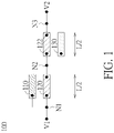
- FIG. 1 shows a section view of a semiconductor device according to a first embodiment of the invention.
- the semiconductor device 100 may be a resistive device, such as a resistor.
- the resistive device may be formed by multiple resistive segments.
- the resistive device or the resistor may be formed by the resistive segments 120 and 122, where the resistive segments 120 and 122 may have the same length or substantially the same length.
- the length of the resistive device or the resistor is L
- the length of the resistive segment 120 may be L/2
- the length of the resistive segment 122 may also be L/2.
- the semiconductor device 100 may comprises terminals N1, N2 and N3, where the terminal N2 is positioned away from the terminal N1 and the terminal N3 is positioned away from the terminals N1 and N2.
- the resistive segment 120 is coupled between the terminals N1 and N2, and the resistive segment 122 is coupled between the terminals N2 and N3.
- the resistive segments 120 and 122 may have resistances that vary non-linearly with applied voltage.
- the resistive segments 120 and 122 may comprise polycrystalline silicon resistive elements.
- At least a first floating plate, such as the floating plate 110 may be disposed physically proximate the resistive segment 120 and a second floating plate, such as the floating plate 130, may be disposed physically proximate the resistive segment 122.
- the floating plate 110 is disposed at one side of the resistive segment 120 (as well as the resistive segments 120 and 122), and the floating plate 130 is disposed at an opposite side of the resistive segment 122 (as well as the resistive segments 120 and 122).
- the floating plate 110 may be a top floating plate and the floating plate 130 may be a bottom floating plate.
- the floating plate 110 may comprise one end being a non-floating end (that is, being coupled to a terminal) and another end being a floating end (that is, not coupled to any terminal).
- the floating plate 130 may also comprise one end being a non-floating end and another end being a floating end (that is, not coupled to any terminal).
- a first end (non-floating end) of the floating plate 110 is coupled to one of the terminal N1 and the terminal N2 and a first end (i.e. the non-floating end) of the floating plate 130 is coupled to one of the terminal N2 and the terminal N3.
- a first end (i.e. the non-floating end) of the floating plate 130 is coupled to one of the terminal N2 and the terminal N3.
- at most one of them is electrically coupled or connected to the terminal N2. Therefore, in some other embodiments of the invention, none of them being electrically coupled or connected to the terminal N2 may also be possible.
- the first end (i.e. the non-floating end) of the floating plate 110 is coupled to the terminal N1 and the first end (i.e. the non-floating end) of the floating plate 130 is coupled to the terminal N2.
- resistive segments are shown in FIG. 1 , the number of resistive segments is not a limit of the invention.
- FIG. 2 shows a section view of a semiconductor device according to a second embodiment of the invention.
- the semiconductor device 200 may be a resistive device, such as a resistor, and may be formed by N resistive segments, such as the resistive segments 220-1, 220-2, 220-3, 220-4...220-(N-1) and 220-N, where the resistive segments 220-1 ⁇ 220-N have the same length or substantially the same length.
- the length of the resistive device or the resistor is L
- the length of each resistive segment may be L/N, where L is a positive number and N is a positive number greater than 1.
- the resistive segments 220-1 ⁇ 220-N may have resistances that vary non-linearly with applied voltage.
- the resistive segments 220-1 ⁇ 220-N may comprise polycrystalline silicon resistive elements.
- multiple floating plates such as the top floating plates 210-1, 210-2...210-(N/2), may be disposed physically proximate and above the resistive segment 220-1, 220-3...220-(N-1), and multiple floating plates, such as the bottom floating plates 230-1, 230-2...230-(N/2), may be disposed physically proximate and under the resistive segment 220-2, 220-4...220-N.
- Each resistive segment may comprise two terminals with one terminal being electrically coupled or connected to a top floating plate and another terminal being electrically coupled or connected to a bottom floating plate.
- each floating plate in FIG. 2 has one end being a floating end.
- non-linearity of resistance of one resistive segment at least partially compensates for non-linearity of resistance of another (as an example, the adjacent) resistive segment.
- the adjacent resistive segment when two different voltages, e.g. the voltages V1 and V2 as shown, are respectively applied to two terminals of the resistive device (or, the resistor formed by the resistive segments), by virtue of the connections of the terminals of the resistive segments to the terminals (or, one ends) of the top floating plates and the terminals (or, one ends) of the bottom floating plates, respectively, the electric fields may be generated between the resistive segments and the top floating plates and between the resistive segments and the bottom floating plates. Consequently, the variation in impedance in a resistive segment is offset by the variation in impedance in one or more adjacent resistive segments.
- the floating plates may be implemented by well process or metal process.
- the top floating plates 210-1, 210-2...210-(N/2) may be implemented by a metal layer and the bottom floating plates 230-1, 230-2...230-(N/2) may be implemented by a substrate well, such as a N-well or P-well.
- the top floating plates 210-1, 210-2...210-(N/2) may be implemented by a first metal layer and the bottom floating plates 230-1, 230-2...230-(N/2) may be implemented by a second metal layer.
- a first isolation layer or isolation region formed of a dielectric material may be interposed between the top floating plates 210-1, 210-2...210-(N/2) and the resistive segments 220-1, 220-3...220-(N-1), and a second isolation layer or isolation region formed of a dielectric material may be interposed between the resistive segments 220-2, 220-4...220-N and the bottom floating plates 230-1, 230-2...230-(N/2).
- the first end (i.e. the non-floating end) of the floating plate 110 may be coupled to the terminal N2 and the first end (i.e. the non-floating end) of the floating plate 130 may be coupled to the terminal N3.
- FIG. 3 shows a section view of a semiconductor device according to a third embodiment of the invention.
- the semiconductor device 300 may be a resistive device, such as a resistor, and may be formed by N resistive segments, such as the resistive segments 320-1, 320-2, 320-3, 320-4...320-(N-1) and 320-N, where the resistive segments 320-1 ⁇ 320-N have the same length or substantially the same length.
- the length of the resistive device or the resistor is L
- the length of each resistive segment may be L/N, where L is a positive number and N is a positive number greater than 1.
- the resistive segments 320-1 ⁇ 320-N may have resistances that vary non-linearly with applied voltage.
- the resistive segments 320-1 ⁇ 320-N may comprise polycrystalline silicon resistive elements.
- multiple floating plates such as the top floating plates 310-1, 310-2... 310-(N/2), may be disposed physically proximate and above the resistive segment 320-1, 320-3...320-(N-1), and multiple floating plates, such as the bottom floating plates 330-1, 330-2...330-(N/2), may be disposed physically proximate and under the resistive segment 320-2, 320-4...320-N.
- Each resistive segment may comprise two terminals with one terminal being electrically coupled or connected to a top floating plate and another terminal being electrically coupled or connected to a bottom floating plate.
- each floating plate in FIG. 3 has one end being a floating end.
- non-linearity of resistance of one resistive segment at least partially compensates for non-linearity of resistance of another (as an example, the adjacent) resistive segment.
- the adjacent resistive segment when two different voltages, e.g. the voltages V1 and V2 as shown, are respectively applied to two terminals of the resistive device (or, the resistor formed by the resistive segments), by virtue of the connections of the terminals of the resistive segments to the terminals (or, one ends) of the top floating plates and the terminals (or, one ends) of the bottom floating plates, respectively, the electric fields may be generated between the resistive segments and the top floating plates and between the resistive segments and the bottom floating plates. Consequently, the variation in impedance in a resistive segment is offset by the variation in impedance in one or more adjacent resistive segments.
- the floating plates may be implemented by well process or metal process.
- the top floating plates 310-1, 310-2...310-(N/2) may be implemented by a metal layer and the bottom floating plates 330-1, 330-2...330-(N/2) may be implemented by a substrate well, such as a N-well or P-well.
- the top floating plates 310-1, 310-2...310-(N/2) may be implemented by a first metal layer and the bottom floating plates 330-1, 330-2...330-(N/2) may be implemented by a second metal layer.
- a first isolation layer or isolation region formed of a dielectric material may be interposed between the top floating plates 310-1, 310-2...310-(N/2) and the resistive segments 320-1, 320-3...320-(N-1), and a second isolation layer or isolation region formed of a dielectric material may be interposed between the resistive segments 320-2, 320-4...320-N and the bottom floating plates 330-1, 330-2...330-(N/2).
- the first end (i.e. the non-floating end) of the floating plate 110 may be coupled to the terminal N1 and the first end (i.e. the non-floating end) of the floating plate 130 may be coupled to the terminal N3. Since it would be no doubt for those skilled in the art to derive the structure of the semiconductor device in further alternative of the first embodiment of the invention with N resistive segments comprised therein based on the teachings of FIG. 2 and FIG. 3 , the corresponding drawing and descriptions are omitted here for brevity.
- one more floating plate may be added and disposed physically proximate the resistive segment 120 and with respect to the floating plate 110 which is also disposed physically proximate the resistive segment 120, and a first end (non-floating end) of this floating plate is coupled to another of the terminal N1 and the terminal N2.
- the two floating plates disposed physically proximate the resistive segment 120 may be disposed at different or opposite side of the resistive segment 120, and both of the two floating plates have one end being a floating end.
- one more floating plate may be added and disposed physically proximate the resistive segment 122 and with respect to the floating plate 130 which is also disposed physically proximate the resistive segment 122, and a first end (non-floating end) of this floating plate is coupled to another of the terminal N2 and the terminal N3.
- the two floating plates disposed physically proximate the resistive segment 122 may be disposed at different or opposite side of the resistive segment 122, and both of the two floating plates have one end being a floating end.
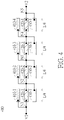
- FIG. 4 shows a section view of a semiconductor device according to a fourth embodiment of the invention.
- the semiconductor device 400 may be a resistive device, such as a resistor, and may be formed by 4 resistive segments, such as the resistive segments 420-1, 420-2, 420-3 and 420-4, where the resistive segments 420-1 ⁇ 420-4 have the same length or substantially the same length.
- the length of the resistive device or the resistor is L
- the length of each resistive segment may be L/4.
- the semiconductor device 400 may comprises terminals N1, N2, N3, N4 and N5.
- the resistive segment 420-1 is coupled between the terminals N1 and N2, the resistive segment 420-2 is coupled between the terminals N2 and N3, the resistive segment 420-3 is coupled between the terminals N3 and N4 and the resistive segment 420-4 is coupled between the terminals N4 and N5.
- the resistive segments 420-1 ⁇ 420-4 may have resistances that vary non-linearly with applied voltage.
- the resistive segments 420-1 ⁇ 420-4 may comprise polycrystalline silicon resistive elements.
- floating plates such as the top floating plates 410-1 ⁇ 410-4, may be disposed physically proximate and above the resistive segment 420-1 ⁇ 420-4, and floating plates, such as the bottom floating plates 430-1 ⁇ 430-4, may be disposed physically proximate and under the resistive segment 420-1 ⁇ 420-4.
- two floating plates 410-1 and 430-1 are disposed physically proximate the resistive segment 420-1 and are disposed at different or opposite side of the resistive segment 420-1, where the first end (i.e. the non-floating end) of the floating plate 410-1 is coupled to the terminal N1 and the first end (i.e. the non-floating end) of the floating plate 430-1 is coupled to the terminal N2.
- two floating plates 410-2 and 430-2 are disposed physically proximate the resistive segment 420-2 and are disposed at different or opposite side of the resistive segment 420-2, where the first end (i.e. the non-floating end) of the floating plate 410-2 is coupled to the terminal N2 and the first end (i.e. the non-floating end) of the floating plate 430-2 is coupled to the terminal N3, and the rest may be deduced by analogy.
- two floating plates disposed at different or opposite side of the resistive segments may be electrically coupled or connected to the same terminal.
- the top floating plate 410-2 and the bottom floating plate 430-1 may both be electrically coupled or connected to the terminal N2
- the top floating plate 410-3 and the bottom floating plate 430-2 may both be electrically coupled or connected to the terminal N3, and so on.
- non-linearity of resistance of one resistive segment at least partially compensates for non-linearity of resistance of another (as an example, the adjacent) resistive segment.
- the adjacent resistive segment when two different voltages, e.g. the voltages V1 and V2 as shown, are respectively applied to two terminals of the resistive device (or, the resistor formed by the resistive segments), by virtue of the connections of the terminals of the resistive segments to the terminals (or, one ends) of the top floating plates and the terminals (or, one ends) of the bottom floating plates, respectively, the electric fields may be generated between the resistive segments and the top floating plates and between the resistive segments and the bottom floating plates. Consequently, the variation in impedance in a resistive segment is offset by the variation in impedance in one or more adjacent resistive segments.
- resistive segments Although four resistive segments is shown in FIG. 4 , the number of resistive segments is not a limit of the invention.
- FIG. 5 shows another exemplary semiconductor device according to a fifth embodiment of the invention, which may be an extension of the structure shown in FIG. 4 .
- the semiconductor device 500 may be a resistive device, such as a resistor, and may be formed by N resistive segments, such as the resistive segments 520-1, 520-2, 520-3, 520-4...520-(N-1) and 520-N, where the resistive segments 520-1 ⁇ 520-N have the same length or substantially the same length.
- the length of the resistive device or the resistor is L
- the length of each resistive segment may be L/N, where L is a positive number and N is a positive number greater than 1.
- each resistive segment may comprise two terminals with one terminal being electrically coupled or connected to a top floating plate and another terminal being electrically coupled or connected to a bottom floating plate.
- each floating plate e.g. in FIG.
- top floating plates 510-1 ⁇ 510-N disposed above the resistive segments 520-1 ⁇ 520-N and the bottom floating plates 530-1 ⁇ 530-N disposed under the resistive segments 520-1 ⁇ 520-N has one end being a floating end.
- the pair of floating plates disposed physically proximate the same resistive segment are electrically coupled or connected to different terminals of that resistive segment.
- the pair of floating plates 510-1 and 530-1 disposed physically proximate the same resistive segment 520-1 are electrically coupled or connected to different terminals N1 and N2 of the resistive segment 520-1
- the pair of floating plates 510-2 and 530-2 disposed physically proximate the same resistive segment 520-2 are electrically coupled or connected to different terminals N2 and N3 of the resistive segment 520-2
- the rest may be deduced by analogy.
- the pair of floating plates disposed physically proximate the same resistive segment may be coupled with different electric potential when two different voltages, e.g. the voltages V1 and V2 as shown, are respectively applied to two terminals of the resistive device.
- a pair of floating plates disposed physically proximate adjacent resistive segment may be electrically coupled or connected to the same terminal.
- the pair of floating plates 510-2 and 530-1 are both electrically coupled or connected to the terminal N2
- the pair of floating plates 510-3 and 530-2 are both electrically coupled or connected to the terminal N3, and the rest may be deduced by analogy.
- non-linearity of resistance of one resistive segment at least partially compensates for non-linearity of resistance of another (as an example, the adjacent) resistive segment.
- the floating plates may be implemented by well process or metal process.
- the top floating plates 510-1 ⁇ 510-N may be implemented by a metal layer and the bottom floating plates 530-1 ⁇ 530-N may be implemented by a substrate well, such as a N-well or P-well.
- the top floating plates 510-1 ⁇ 510-N may be implemented by a first metal layer and the bottom floating plates 530-1 ⁇ 530-N may be implemented by a second metal layer.
- a first isolation layer or isolation region formed of a dielectric material may be interposed between the top floating plates 510-1 ⁇ 510-N and the resistive segments 520-1 ⁇ 520-N, and a second isolation layer or isolation region formed of a dielectric material may be interposed between the resistive segments 520-1 ⁇ 520-N and the bottom floating plates 530-1 ⁇ 530-N.
Landscapes
- Engineering & Computer Science (AREA)
- Microelectronics & Electronic Packaging (AREA)
- Manufacturing & Machinery (AREA)
- Physics & Mathematics (AREA)
- Electromagnetism (AREA)
- Semiconductor Integrated Circuits (AREA)
- Lead Frames For Integrated Circuits (AREA)
Abstract
Description
- This application claims the benefit of
U.S. Provisional Application No. 63/213,797, filed on June 23rd, 2021 - Resistors are optimally linear devices, that is, the output is directly proportional to the input. However, achieving a highly linear resistor in an integrated circuit is difficult or expensive. For example, the resistance of polycrystalline silicon (also referred to as polysilicon, poly-Si or simply poly) varies with the applied voltage in a non-linear fashion in the presence of an electric field. This non-linearity is caused by an accumulation of carriers (and thus reduced resistance) in the presence of a positive electric field, or conversely, by a depletion of carriers (and thus increased resistance) in the presence of a negative electric field.
- Because such non-linearity is undesirable in many applications, a novel resistor structure with more refined coupling effect for improved linearity of resistance is highly required.
- A semiconductor device according to the invention is defined in
independent claim 1. The dependent claims define preferred embodiments thereof. According to an embodiment of the invention, a semiconductor device comprises a first terminal, a second terminal positioned away from the first terminal, a first resistive segment coupled between the first terminal and the second terminal, a third terminal positioned away from the first terminal and the second terminal, a second resistive segment coupled between the second terminal and third terminal, a first floating plate disposed physically proximate the first resistive segment and comprising a first end coupled to one of the first terminal and the second terminal, and a second floating plate disposed physically proximate the second resistive segment and comprising a first end coupled to one of the second terminal and the third terminal. - According to another embodiment of the invention, a semiconductor device comprises a first terminal, a second terminal positioned away from the first terminal, a first resistive segment coupled between the first terminal and the second terminal, a third terminal positioned away from the first terminal and the second terminal, a second resistive segment coupled between the second terminal and third terminal, a first floating plate disposed physically proximate the first resistive segment and comprising a first end coupled to one of the first terminal and the second terminal and a second end being a floating end, and a second floating plate disposed physically proximate the second resistive segment and comprising a first end coupled to one of the second terminal and the third terminal and a second end being a floating end. At most one of the first end of the first floating plate and the first end of the second floating plate is electrically coupled to the second terminal.
- According to another embodiment of the invention, a semiconductor device comprises a first terminal, a second terminal positioned away from the first terminal, a first resistive segment coupled between the first terminal and the second terminal, a third terminal positioned away from the first terminal and the second terminal, a second resistive segment coupled between the second terminal and third terminal, a first floating plate disposed physically proximate the first resistive segment and comprising a first end coupled to the first terminal and a second end being a floating end, a second floating plate disposed physically proximate the second resistive segment and comprising a first end coupled to the third terminal and a second end being a floating end, a third floating plate disposed physically proximate the first resistive segment and comprising a first end coupled to the second terminal and a second end being a floating end, and a fourth floating plate disposed physically proximate the second resistive segment and comprising a first end coupled to the second terminal and a second end being a floating end. The first floating plate is disposed at one side of the first resistive segment and the third floating plate is disposed at another side of the first resistive segment, and the second floating plate is disposed at one side of the second resistive segment and the fourth floating plate is disposed at another side of the second resistive segment.
- These and other objectives of the present invention will no doubt become obvious to those of ordinary skill in the art after reading the following detailed description of the preferred embodiment that is illustrated in the various figures and drawings.
-
-
FIG. 1 shows a section view of a semiconductor device according to a first embodiment of the invention. -
FIG. 2 shows a section view of a semiconductor device according to a second embodiment of the invention. -
FIG. 3 shows a section view of a semiconductor device according to a third embodiment of the invention. -
FIG. 4 shows a section view of a semiconductor device according to a fourth embodiment of the invention. -
FIG. 5 shows another exemplary semiconductor device according to t a fifth embodiment of the invention. -
FIG. 1 shows a section view of a semiconductor device according to a first embodiment of the invention. Preferably, thesemiconductor device 100 may be a resistive device, such as a resistor. In the embodiments of the invention, the resistive device may be formed by multiple resistive segments. As shown inFIG. 1 , the resistive device or the resistor may be formed by theresistive segments resistive segments resistive segment 120 may be L/2 and the length of theresistive segment 122 may also be L/2. - The
semiconductor device 100 may comprises terminals N1, N2 and N3, where the terminal N2 is positioned away from the terminal N1 and the terminal N3 is positioned away from the terminals N1 and N2. Theresistive segment 120 is coupled between the terminals N1 and N2, and theresistive segment 122 is coupled between the terminals N2 and N3. - Preferably, the
resistive segments resistive segments - In one of the proposed structures with more refined coupling effect for supreme linearity, as shown in
FIG. 1 , at least a first floating plate, such as thefloating plate 110, may be disposed physically proximate theresistive segment 120 and a second floating plate, such as thefloating plate 130, may be disposed physically proximate theresistive segment 122. Preferably, thefloating plate 110 is disposed at one side of the resistive segment 120 (as well as theresistive segments 120 and 122), and thefloating plate 130 is disposed at an opposite side of the resistive segment 122 (as well as theresistive segments 120 and 122). In addition, preferably, thefloating plate 110 may be a top floating plate and thefloating plate 130 may be a bottom floating plate. - The
floating plate 110 may comprise one end being a non-floating end (that is, being coupled to a terminal) and another end being a floating end (that is, not coupled to any terminal). Thefloating plate 130 may also comprise one end being a non-floating end and another end being a floating end (that is, not coupled to any terminal). - As an example, a first end (non-floating end) of the
floating plate 110 is coupled to one of the terminal N1 and the terminal N2 and a first end (i.e. the non-floating end) of thefloating plate 130 is coupled to one of the terminal N2 and the terminal N3. Note that in some embodiments of the invention, at most one of them is electrically coupled or connected to the terminal N2. Therefore, in some other embodiments of the invention, none of them being electrically coupled or connected to the terminal N2 may also be possible. - In the first embodiment of the invention, as shown in
FIG. 1 , the first end (i.e. the non-floating end) of thefloating plate 110 is coupled to the terminal N1 and the first end (i.e. the non-floating end) of thefloating plate 130 is coupled to the terminal N2. - It is to be noted that although two resistive segments are shown in
FIG. 1 , the number of resistive segments is not a limit of the invention. -
FIG. 2 shows a section view of a semiconductor device according to a second embodiment of the invention. Preferably, thesemiconductor device 200 may be a resistive device, such as a resistor, and may be formed by N resistive segments, such as the resistive segments 220-1, 220-2, 220-3, 220-4...220-(N-1) and 220-N, where the resistive segments 220-1~220-N have the same length or substantially the same length. Suppose that the length of the resistive device or the resistor is L, the length of each resistive segment may be L/N, where L is a positive number and N is a positive number greater than 1. - Preferably, the resistive segments 220-1~220-N may have resistances that vary non-linearly with applied voltage. Preferably, the resistive segments 220-1~220-N may comprise polycrystalline silicon resistive elements.
- In the proposed structures with more refined coupling effect for supreme linearity, as shown in
FIG. 2 , multiple floating plates, such as the top floating plates 210-1, 210-2...210-(N/2), may be disposed physically proximate and above the resistive segment 220-1, 220-3...220-(N-1), and multiple floating plates, such as the bottom floating plates 230-1, 230-2...230-(N/2), may be disposed physically proximate and under the resistive segment 220-2, 220-4...220-N. - Each resistive segment, except for the last resistive segment 220-N, may comprise two terminals with one terminal being electrically coupled or connected to a top floating plate and another terminal being electrically coupled or connected to a bottom floating plate. In addition, each floating plate in
FIG. 2 has one end being a floating end. - By implementing the proposed structure, non-linearity of resistance of one resistive segment at least partially compensates for non-linearity of resistance of another (as an example, the adjacent) resistive segment. To be more specific, when two different voltages, e.g. the voltages V1 and V2 as shown, are respectively applied to two terminals of the resistive device (or, the resistor formed by the resistive segments), by virtue of the connections of the terminals of the resistive segments to the terminals (or, one ends) of the top floating plates and the terminals (or, one ends) of the bottom floating plates, respectively, the electric fields may be generated between the resistive segments and the top floating plates and between the resistive segments and the bottom floating plates. Consequently, the variation in impedance in a resistive segment is offset by the variation in impedance in one or more adjacent resistive segments.
- Preferably, the floating plates may be implemented by well process or metal process. As an example, the top floating plates 210-1, 210-2...210-(N/2) may be implemented by a metal layer and the bottom floating plates 230-1, 230-2...230-(N/2) may be implemented by a substrate well, such as a N-well or P-well. As another example, the top floating plates 210-1, 210-2...210-(N/2) may be implemented by a first metal layer and the bottom floating plates 230-1, 230-2...230-(N/2) may be implemented by a second metal layer. In addition, a first isolation layer or isolation region formed of a dielectric material may be interposed between the top floating plates 210-1, 210-2...210-(N/2) and the resistive segments 220-1, 220-3...220-(N-1), and a second isolation layer or isolation region formed of a dielectric material may be interposed between the resistive segments 220-2, 220-4...220-N and the bottom floating plates 230-1, 230-2...230-(N/2).
- Referring back to
FIG. 1 , in an alternative of the first embodiment of the invention, the first end (i.e. the non-floating end) of thefloating plate 110 may be coupled to the terminal N2 and the first end (i.e. the non-floating end) of thefloating plate 130 may be coupled to the terminal N3. -
FIG. 3 shows a section view of a semiconductor device according to a third embodiment of the invention. Preferably, thesemiconductor device 300 may be a resistive device, such as a resistor, and may be formed by N resistive segments, such as the resistive segments 320-1, 320-2, 320-3, 320-4...320-(N-1) and 320-N, where the resistive segments 320-1~320-N have the same length or substantially the same length. Suppose that the length of the resistive device or the resistor is L, the length of each resistive segment may be L/N, where L is a positive number and N is a positive number greater than 1. - Preferably, the resistive segments 320-1~320-N may have resistances that vary non-linearly with applied voltage. Preferably, the resistive segments 320-1~320-N may comprise polycrystalline silicon resistive elements.
- In the proposed structures with more refined coupling effect for supreme linearity, as shown in
FIG. 3 , multiple floating plates, such as the top floating plates 310-1, 310-2... 310-(N/2), may be disposed physically proximate and above the resistive segment 320-1, 320-3...320-(N-1), and multiple floating plates, such as the bottom floating plates 330-1, 330-2...330-(N/2), may be disposed physically proximate and under the resistive segment 320-2, 320-4...320-N. - Each resistive segment, except for the first resistive segment 320-1, may comprise two terminals with one terminal being electrically coupled or connected to a top floating plate and another terminal being electrically coupled or connected to a bottom floating plate. In addition, each floating plate in
FIG. 3 has one end being a floating end. - By implementing the proposed structure, non-linearity of resistance of one resistive segment at least partially compensates for non-linearity of resistance of another (as an example, the adjacent) resistive segment. To be more specific, when two different voltages, e.g. the voltages V1 and V2 as shown, are respectively applied to two terminals of the resistive device (or, the resistor formed by the resistive segments), by virtue of the connections of the terminals of the resistive segments to the terminals (or, one ends) of the top floating plates and the terminals (or, one ends) of the bottom floating plates, respectively, the electric fields may be generated between the resistive segments and the top floating plates and between the resistive segments and the bottom floating plates. Consequently, the variation in impedance in a resistive segment is offset by the variation in impedance in one or more adjacent resistive segments.
- Preferably, the floating plates may be implemented by well process or metal process. As an example, the top floating plates 310-1, 310-2...310-(N/2) may be implemented by a metal layer and the bottom floating plates 330-1, 330-2...330-(N/2) may be implemented by a substrate well, such as a N-well or P-well. As another example, the top floating plates 310-1, 310-2...310-(N/2) may be implemented by a first metal layer and the bottom floating plates 330-1, 330-2...330-(N/2) may be implemented by a second metal layer. In addition, a first isolation layer or isolation region formed of a dielectric material may be interposed between the top floating plates 310-1, 310-2...310-(N/2) and the resistive segments 320-1, 320-3...320-(N-1), and a second isolation layer or isolation region formed of a dielectric material may be interposed between the resistive segments 320-2, 320-4...320-N and the bottom floating plates 330-1, 330-2...330-(N/2).
- Again, referring back to
FIG. 1 , in a further alternative of the first embodiment of the invention, the first end (i.e. the non-floating end) of the floatingplate 110 may be coupled to the terminal N1 and the first end (i.e. the non-floating end) of the floatingplate 130 may be coupled to the terminal N3. Since it would be no doubt for those skilled in the art to derive the structure of the semiconductor device in further alternative of the first embodiment of the invention with N resistive segments comprised therein based on the teachings ofFIG. 2 andFIG. 3 , the corresponding drawing and descriptions are omitted here for brevity. - In a still further alternative of the first embodiment of the invention, based on the structure shown in
FIG. 1 , one more floating plate may be added and disposed physically proximate theresistive segment 120 and with respect to the floatingplate 110 which is also disposed physically proximate theresistive segment 120, and a first end (non-floating end) of this floating plate is coupled to another of the terminal N1 and the terminal N2. Note that the two floating plates disposed physically proximate theresistive segment 120 may be disposed at different or opposite side of theresistive segment 120, and both of the two floating plates have one end being a floating end. - Similarly, one more floating plate may be added and disposed physically proximate the
resistive segment 122 and with respect to the floatingplate 130 which is also disposed physically proximate theresistive segment 122, and a first end (non-floating end) of this floating plate is coupled to another of the terminal N2 and the terminal N3. Note that the two floating plates disposed physically proximate theresistive segment 122 may be disposed at different or opposite side of theresistive segment 122, and both of the two floating plates have one end being a floating end. -
FIG. 4 shows a section view of a semiconductor device according to a fourth embodiment of the invention. Preferably, thesemiconductor device 400 may be a resistive device, such as a resistor, and may be formed by 4 resistive segments, such as the resistive segments 420-1, 420-2, 420-3 and 420-4, where the resistive segments 420-1~420-4 have the same length or substantially the same length. Suppose that the length of the resistive device or the resistor is L, the length of each resistive segment may be L/4. - The
semiconductor device 400 may comprises terminals N1, N2, N3, N4 and N5. The resistive segment 420-1 is coupled between the terminals N1 and N2, the resistive segment 420-2 is coupled between the terminals N2 and N3, the resistive segment 420-3 is coupled between the terminals N3 and N4 and the resistive segment 420-4 is coupled between the terminals N4 and N5. - Preferably, the resistive segments 420-1~420-4 may have resistances that vary non-linearly with applied voltage. Preferably, the resistive segments 420-1~420-4 may comprise polycrystalline silicon resistive elements.
- In the proposed structures with more refined coupling effect for supreme linearity, as shown in
FIG. 4 , floating plates, such as the top floating plates 410-1~410-4, may be disposed physically proximate and above the resistive segment 420-1~420-4, and floating plates, such as the bottom floating plates 430-1~430-4, may be disposed physically proximate and under the resistive segment 420-1~420-4. - As shown in
FIG. 4 , two floating plates 410-1 and 430-1 are disposed physically proximate the resistive segment 420-1 and are disposed at different or opposite side of the resistive segment 420-1, where the first end (i.e. the non-floating end) of the floating plate 410-1 is coupled to the terminal N1 and the first end (i.e. the non-floating end) of the floating plate 430-1 is coupled to the terminal N2. Similarly, two floating plates 410-2 and 430-2 are disposed physically proximate the resistive segment 420-2 and are disposed at different or opposite side of the resistive segment 420-2, where the first end (i.e. the non-floating end) of the floating plate 410-2 is coupled to the terminal N2 and the first end (i.e. the non-floating end) of the floating plate 430-2 is coupled to the terminal N3, and the rest may be deduced by analogy. - In the fourth embodiment, two floating plates disposed at different or opposite side of the resistive segments may be electrically coupled or connected to the same terminal. As an example, the top floating plate 410-2 and the bottom floating plate 430-1 may both be electrically coupled or connected to the terminal N2, the top floating plate 410-3 and the bottom floating plate 430-2 may both be electrically coupled or connected to the terminal N3, and so on.
- By implementing the proposed structure, non-linearity of resistance of one resistive segment at least partially compensates for non-linearity of resistance of another (as an example, the adjacent) resistive segment. To be more specific, when two different voltages, e.g. the voltages V1 and V2 as shown, are respectively applied to two terminals of the resistive device (or, the resistor formed by the resistive segments), by virtue of the connections of the terminals of the resistive segments to the terminals (or, one ends) of the top floating plates and the terminals (or, one ends) of the bottom floating plates, respectively, the electric fields may be generated between the resistive segments and the top floating plates and between the resistive segments and the bottom floating plates. Consequently, the variation in impedance in a resistive segment is offset by the variation in impedance in one or more adjacent resistive segments.
- It is to be noted that although four resistive segments is shown in
FIG. 4 , the number of resistive segments is not a limit of the invention. -
FIG. 5 shows another exemplary semiconductor device according to a fifth embodiment of the invention, which may be an extension of the structure shown inFIG. 4 . Thesemiconductor device 500 may be a resistive device, such as a resistor, and may be formed by N resistive segments, such as the resistive segments 520-1, 520-2, 520-3, 520-4...520-(N-1) and 520-N, where the resistive segments 520-1~520-N have the same length or substantially the same length. Suppose that the length of the resistive device or the resistor is L, the length of each resistive segment may be L/N, where L is a positive number and N is a positive number greater than 1. - In the proposed structures with more refined coupling effect for supreme linearity, as shown in
FIG. 5 , a pair of floating plates, comprising one top floating plate and one bottom floating plate, may be disposed physically proximate one resistive segment and disposed at different sides or opposite sides of that resistive segment. Therefore, in the fourth and fifth embodiments, each resistive segment may comprise two terminals with one terminal being electrically coupled or connected to a top floating plate and another terminal being electrically coupled or connected to a bottom floating plate. In addition, each floating plate, e.g. inFIG. 5 , such as the top floating plates 510-1∼510-N disposed above the resistive segments 520-1~520-N and the bottom floating plates 530-1~530-N disposed under the resistive segments 520-1~520-N, has one end being a floating end. - Note that in the fourth and fifth embodiments of the invention, the pair of floating plates disposed physically proximate the same resistive segment are electrically coupled or connected to different terminals of that resistive segment. As an example, the pair of floating plates 510-1 and 530-1 disposed physically proximate the same resistive segment 520-1 are electrically coupled or connected to different terminals N1 and N2 of the resistive segment 520-1, the pair of floating plates 510-2 and 530-2 disposed physically proximate the same resistive segment 520-2 are electrically coupled or connected to different terminals N2 and N3 of the resistive segment 520-2, and the rest may be deduced by analogy. In this manner, the pair of floating plates disposed physically proximate the same resistive segment may be coupled with different electric potential when two different voltages, e.g. the voltages V1 and V2 as shown, are respectively applied to two terminals of the resistive device.
- In addition, a pair of floating plates disposed physically proximate adjacent resistive segment may be electrically coupled or connected to the same terminal. As an example, the pair of floating plates 510-2 and 530-1 are both electrically coupled or connected to the terminal N2, the pair of floating plates 510-3 and 530-2 are both electrically coupled or connected to the terminal N3, and the rest may be deduced by analogy.
- Similarly, by implementing the proposed structure, non-linearity of resistance of one resistive segment at least partially compensates for non-linearity of resistance of another (as an example, the adjacent) resistive segment.
- Preferably, the floating plates may be implemented by well process or metal process. As an example, the top floating plates 510-1∼510-N may be implemented by a metal layer and the bottom floating plates 530-1~530-N may be implemented by a substrate well, such as a N-well or P-well. As another example, the top floating plates 510-1∼510-N may be implemented by a first metal layer and the bottom floating plates 530-1~530-N may be implemented by a second metal layer. In addition, a first isolation layer or isolation region formed of a dielectric material may be interposed between the top floating plates 510-1∼510-N and the resistive segments 520-1~520-N, and a second isolation layer or isolation region formed of a dielectric material may be interposed between the resistive segments 520-1~520-N and the bottom floating plates 530-1~530-N.
- By implementing the proposed resistor structures with more refined coupling effect as illustrated above in the embodiments of the invention, linearity of resistance of the resistor or resistive device is greatly improved.
- Those skilled in the art will readily observe that numerous modifications and alterations of the device and method may be made while retaining the teachings of the invention. Accordingly, the above disclosure should be construed as limited only by the metes and bounds of the appended claims.
Claims (15)
- A semiconductor device (100; 200; 300; 400; 500), comprising:a first terminal (N1);a second terminal (N2), positioned away from the first terminal (N1);a first resistive segment (120; 220-1; 320-1; 420-1; 520-1), coupled between the first terminal (N1) and the second terminal (N2);a third terminal (N3), positioned away from the first terminal (N1) and the second terminal (N2);a second resistive segment (122; 220-2; 320-2; 420-2; 520-2), coupled between the second terminal (N2) and third terminal (N3);a first floating plate (110; 210-1; 310-1; 410-1; 510-1), disposed physically proximate the first resistive segment (120; 220-1; 320-1; 420-1; 520-1) and comprising a first end coupled to one of the first terminal (N1) and the second terminal (N2); anda second floating plate (130; 230-1; 330-1; 430-2; 530-2), disposed physically proximate the second resistive segment (122; 220-2; 320-2; 420-2; 520-2) and comprising a first end coupled to one of the second terminal (N2) and the third terminal (N3).
- The semiconductor device (300) of claim 1, wherein the first floating plate (310-1) further comprises a second end which is a floating end, and when the first end of the first floating plate (310-1) is coupled to the second terminal (N2), the first end of the second floating plate (330-1) is coupled to the third terminal (N3).
- The semiconductor device (100; 200) of claim 1 or 2, wherein the second floating plate (130; 230-1) further comprises a second end which is a floating end, and when the first end of the second floating plate (130; 230-1) is coupled to the second terminal (N2), the first end of the first floating plate (110; 210-1) is coupled to the first terminal (N1).
- The semiconductor device (100; 200; 300; 400; 500) of any one of claims 1 to 3, wherein the first floating plate (110; 210-1; 310-1; 410-1; 510-1) is disposed at one side of the first resistive segment (120; 220-1; 320-1; 420-1; 520-1) and the second resistive segment (122; 220-2; 320-2; 420-2; 520-2), and the second floating plate (130; 230-1; 330-1; 430-2; 530-2) is disposed at an opposite side of the first resistive segment (120; 220-1; 320-1; 420-1; 520-1) and the second resistive segment (122; 220-2; 320-2; 420-2; 520-2).
- The semiconductor device (400; 500) of any one of claims 1 to 4, further comprising:a third floating plate (430-1; 530-1), disposed physically proximate the first resistive segment (420-1; 520-1) and comprising a first end coupled to another of the first terminal (N1) and the second terminal (N2),wherein the first floating plate (410-1; 510-1) is disposed at one side of the first resistive segment (420-1; 520-1) and the third floating plate (430-1; 530-1) is disposed at an opposite side of the first resistive segment (420-1; 520-1).
- The semiconductor device (400; 500) of any one of claims 1 to 5, further comprising:a fourth floating plate (410-2; 510-2), disposed physically proximate the second resistive segment (420-2; 520-2) and comprising a first end coupled to another of the second terminal (N2) and the third terminal (N3),wherein the second floating plate (430-2; 530-2) is disposed at one side of the second resistive segment (420-2; 520-2) and the fourth floating plate (410-2; 510-2) is disposed at an opposite side of the second resistive segment (420-2; 520-2).
- The semiconductor device (100; 200; 300; 400; 500) of claim 1, whereinthe first floating plate (110; 210-1; 310-1; 410-1; 510-1) comprises a second end being a floating end,the second floating plate (130; 230-1; 330-1; 430-2; 530-2) comprises a second end being a floating end, andat most one of the first end of the first floating plate (110; 210-1; 310-1; 410-1; 510-1) and the first end of the second floating plate (130; 230-1; 330-1; 430-2; 530-2) is electrically coupled to the second terminal (N2).
- The semiconductor device (100; 200; 300) of claim 7, wherein when the first end of the first floating plate (110; 210-1; 310-1) is coupled to the second terminal (N2), the first end of the second floating plate (130; 230-1; 330-1; 430-2; 530-2) is coupled to the third terminal (N3), and when the first end of the second floating plate (130; 230-1; 330-1; 430-2; 530-2) is coupled to the second terminal (N2), the first end of the first floating plate (110; 210-1; 310-1) is coupled to the first terminal (N1).
- The semiconductor device (100; 200; 300; 400; 500) of claim 7 or 8, wherein the first floating plate (110; 210-1; 310-1; 410-1; 510-1) is disposed at one side of the first resistive segment (120; 220-1; 320-1; 420-1; 520-1) and the second resistive segment (122; 220-2; 320-2; 420-2; 520-2), and the second floating plate (130; 230-1; 330-1; 430-2; 530-2) is disposed at an opposite side of the first resistive segment (120; 220-1; 320-1; 420-1; 520-1) and the second resistive segment (122; 220-2; 320-2; 420-2; 520-2).
- The semiconductor device (400; 500) of any one of claims 7 to 9, further comprising:a third floating plate (430-1; 530-1), disposed physically proximate the first resistive segment (420-1; 520-1) and comprising a first end coupled to another of the first terminal (N1) and the second terminal (N2) and a second end being a floating end,wherein the first floating plate (410-1; 510-1) is disposed at one side of the first resistive segment (420-1; 520-1) and the third floating plate (430-1; 530-1) is disposed at an opposite side of the first resistive segment (420-1; 520-1).
- The semiconductor device (400; 500) of any one of claims 7 to 10, further comprising:a fourth floating plate (410-2; 510-2), disposed physically proximate the second resistive segment (420-2; 520-2) and comprising a first end coupled to another of the second terminal (N2) and the third terminal (N3) and a second end being a floating end,wherein the second floating plate (430-2; 530-2) is disposed at one side of the second resistive segment (420-2; 520-2) and the fourth floating plate (410-2; 510-2) is disposed at an opposite side of the second resistive segment (420-2; 520-2).
- The semiconductor device (400; 500) of any one of claims 7 to 9, further comprising:a third floating plate (430-1; 530-1), disposed physically proximate the first resistive segment (420-1; 520-1); anda fourth floating plate (410-2; 510-2), disposed physically proximate the second resistive segment (420-2; 520-2),wherein the first floating plate (410-1; 510-1) is disposed at one side of the first resistive segment (420-1; 520-1) and the third floating plate (430-1; 530-1) is disposed at another side of the first resistive segment (420-1; 520-1), the second floating plate (430-2; 530-2) is disposed at one side of the second resistive segment (420-2; 520-2) and the fourth floating plate (410-2; 510-2) is disposed at another side of the second resistive segment (420-2; 520-2), andwherein when the first end of the first floating plate (410-1; 510-1) is coupled to the first terminal (N1), the first end of the second floating plate (430-2; 530-2) is coupled to the third terminal (N3), and a first end of the third floating plate (430-1; 530-1) and a first end of the fourth floating plate (410-2; 510-2) are both coupled to the second terminal (N2).
- The semiconductor device (400; 500) of claim 1, whereinthe first floating plate (410-1; 510-1) comprises a first end coupled to the first terminal (N1) and a second end being a floating end; andthe second floating plate (430-2; 530-2) comprises a first end coupled to the third terminal (N3) and a second end being a floating end; andfurther comprising:a third floating plate (430-1; 530-1), disposed physically proximate the first resistive segment (420-1; 520-1) and comprising a first end coupled to the second terminal (N2) and a second end being a floating end; anda fourth floating plate (410-2; 510-2), disposed physically proximate the second resistive segment (420-2; 520-2) and comprising a first end coupled to the second terminal (N2) and a second end being a floating end,wherein the first floating plate (410-1; 510-1) is disposed at one side of the first resistive segment (420-1; 520-1) and the third floating plate (430-1; 530-1) is disposed at another side of the first resistive segment (420-1; 520-1), and the second floating plate (430-2; 530-2) is disposed at one side of the second resistive segment (420-2; 520-2) and the fourth floating plate (410-2; 510-2) is disposed at another side of the second resistive segment (420-2; 520-2).
- The semiconductor device (100; 200; 300; 400; 500) of any one of claims 1 to 13, wherein the first resistive segment (120; 220-1; 320-1; 420-1; 520-1) and the second resistive segment (122; 220-2; 320-2; 420-2; 520-2) have substantially a same length and/or comprise polycrystalline silicon resistive elements.
- The semiconductor device (100; 200; 300; 400; 500) of any one of claims 1 to 14, further comprising:a first isolation layer, interposed between the first resistive segment (120; 220-1; 320-1; 420-1; 520-1) and the first floating plate (110; 210-1; 310-1; 410-1; 510-1); anda second isolation layer, interposed between the second resistive segment (122; 220-2; 320-2; 420-2; 520-2) and the second floating plate (130; 230-1; 330-1; 430-2; 530-2).
Applications Claiming Priority (2)
| Application Number | Priority Date | Filing Date | Title |
|---|---|---|---|
| US202163213797P | 2021-06-23 | 2021-06-23 | |
| US17/830,348 US12211887B2 (en) | 2021-06-23 | 2022-06-02 | Semiconductor devices having a resistor structure with more refined coupling effect for improved linearity of resistance |
Publications (1)
| Publication Number | Publication Date |
|---|---|
| EP4109475A1 true EP4109475A1 (en) | 2022-12-28 |
Family
ID=82839353
Family Applications (1)
| Application Number | Title | Priority Date | Filing Date |
|---|---|---|---|
| EP22178601.5A Pending EP4109475A1 (en) | 2021-06-23 | 2022-06-13 | Semiconductor devices having a resistor structure with more refined coupling effect for improved linearity of resistance |
Country Status (4)
| Country | Link |
|---|---|
| US (1) | US12211887B2 (en) |
| EP (1) | EP4109475A1 (en) |
| CN (1) | CN115513185A (en) |
| TW (1) | TWI900777B (en) |
Citations (3)
| Publication number | Priority date | Publication date | Assignee | Title |
|---|---|---|---|---|
| US6369409B1 (en) * | 1995-08-24 | 2002-04-09 | Seiko Instruments Inc. | Semiconductor device and method of manufacturing the same |
| US20090085657A1 (en) * | 2007-09-28 | 2009-04-02 | Hua Yang | Compensation of field effect on polycrystalline resistors |
| US7586162B1 (en) * | 2004-05-14 | 2009-09-08 | Peregrine Semiconductor Corporation | High-value integrated resistor and method of making |
Family Cites Families (9)
| Publication number | Priority date | Publication date | Assignee | Title |
|---|---|---|---|---|
| KR100535062B1 (en) | 2001-06-04 | 2005-12-07 | 마츠시타 덴끼 산교 가부시키가이샤 | High-voltage semiconductor device |
| US7176781B2 (en) * | 2004-09-29 | 2007-02-13 | Agere Systems Inc | Structure and method for adjusting integrated circuit resistor value |
| CN103620706A (en) * | 2011-06-17 | 2014-03-05 | 美国亚德诺半导体公司 | Offset reducing resistor circuit |
| SG11201405269UA (en) | 2012-02-29 | 2014-11-27 | Mitsui Chemicals Tohcello Inc | Sheet set for encapsulating solar battery |
| US10107873B2 (en) * | 2016-03-10 | 2018-10-23 | Allegro Microsystems, Llc | Electronic circuit for compensating a sensitivity drift of a hall effect element due to stress |
| US10573711B2 (en) * | 2017-07-13 | 2020-02-25 | Semiconductor Components Industries, Llc | Semiconductor device resistor including vias and multiple metal layers |
| JP7027176B2 (en) * | 2018-01-22 | 2022-03-01 | ラピスセミコンダクタ株式会社 | Semiconductor device |
| CN114400216A (en) * | 2018-04-25 | 2022-04-26 | 华为技术有限公司 | Polycrystalline silicon resistor |
| TWI793186B (en) | 2018-10-03 | 2023-02-21 | 日商琳得科股份有限公司 | Method for producing laminate and hardened seal |
-
2022
- 2022-06-02 US US17/830,348 patent/US12211887B2/en active Active
- 2022-06-07 TW TW111120955A patent/TWI900777B/en active
- 2022-06-08 CN CN202210648048.8A patent/CN115513185A/en active Pending
- 2022-06-13 EP EP22178601.5A patent/EP4109475A1/en active Pending
Patent Citations (3)
| Publication number | Priority date | Publication date | Assignee | Title |
|---|---|---|---|---|
| US6369409B1 (en) * | 1995-08-24 | 2002-04-09 | Seiko Instruments Inc. | Semiconductor device and method of manufacturing the same |
| US7586162B1 (en) * | 2004-05-14 | 2009-09-08 | Peregrine Semiconductor Corporation | High-value integrated resistor and method of making |
| US20090085657A1 (en) * | 2007-09-28 | 2009-04-02 | Hua Yang | Compensation of field effect on polycrystalline resistors |
Also Published As
| Publication number | Publication date |
|---|---|
| CN115513185A (en) | 2022-12-23 |
| TW202316452A (en) | 2023-04-16 |
| US12211887B2 (en) | 2025-01-28 |
| US20220416009A1 (en) | 2022-12-29 |
| TWI900777B (en) | 2025-10-11 |
Similar Documents
| Publication | Publication Date | Title |
|---|---|---|
| US11888468B2 (en) | Tuning capacitance to enhance FET stack voltage withstand | |
| EP0555995A2 (en) | Monolithic high-voltage capacitor | |
| USRE46486E1 (en) | Semiconductor pressure sensor | |
| US20090002916A1 (en) | Interdigital capacitor | |
| US7598592B2 (en) | Capacitor structure for integrated circuit | |
| JP5491160B2 (en) | Microcapacitor element and semiconductor device using the same | |
| CN105896145B (en) | Connector | |
| TW200729518A (en) | Integrated capacitor arrangement for ultrahigh capacitance values | |
| TW200513023A (en) | Circuit for signal amplification and use of the same in active matrix devices | |
| JP2011015289A (en) | Semiconductor integrated circuit device | |
| KR102209244B1 (en) | Capacitive pressure sensor and input device | |
| WO2010002559A1 (en) | Dynamically-driven deep n-well circuit | |
| US7915995B2 (en) | Compensation of field effect on polycrystalline resistors | |
| TW303545B (en) | Gain controlled amplification circuit having differential amplifier | |
| US4626881A (en) | Capacitor produced of a layer combination of metal, insulator and semiconductor | |
| US7619873B2 (en) | Feedthrough multilayer capacitor | |
| KR20040008851A (en) | Metal-Insulator-Metal capacitor having constant capacitance and semiconductor device having the capacitor | |
| US20180247998A1 (en) | Apparatuses and methods for semiconductor circuit layout | |
| US10447202B2 (en) | Apparatus for communication across a capacitively coupled channel | |
| US20160276071A1 (en) | Apparatus and methods for generating a precise resistor | |
| US12211887B2 (en) | Semiconductor devices having a resistor structure with more refined coupling effect for improved linearity of resistance | |
| US9520355B2 (en) | Voltage and temperature independent MIM capacitors | |
| US4366455A (en) | Switched-capacity amplifier, switched-capacity filter and charge-transfer filter comprising such an amplifier | |
| US11049855B2 (en) | Tunable capacitive compensation for RF switch FET stacks | |
| CN102569299A (en) | Depletion type MOS (metal oxide semiconductor) resistor and formation method thereof |
Legal Events
| Date | Code | Title | Description |
|---|---|---|---|
| PUAI | Public reference made under article 153(3) epc to a published international application that has entered the european phase |
Free format text: ORIGINAL CODE: 0009012 |
|
| STAA | Information on the status of an ep patent application or granted ep patent |
Free format text: STATUS: THE APPLICATION HAS BEEN PUBLISHED |
|
| AK | Designated contracting states |
Kind code of ref document: A1 Designated state(s): AL AT BE BG CH CY CZ DE DK EE ES FI FR GB GR HR HU IE IS IT LI LT LU LV MC MK MT NL NO PL PT RO RS SE SI SK SM TR |
|
| STAA | Information on the status of an ep patent application or granted ep patent |
Free format text: STATUS: REQUEST FOR EXAMINATION WAS MADE |
|
| 17P | Request for examination filed |
Effective date: 20230620 |
|
| RBV | Designated contracting states (corrected) |
Designated state(s): AL AT BE BG CH CY CZ DE DK EE ES FI FR GB GR HR HU IE IS IT LI LT LU LV MC MK MT NL NO PL PT RO RS SE SI SK SM TR |
|
| P01 | Opt-out of the competence of the unified patent court (upc) registered |
Effective date: 20230627 |