EP4109151A1 - Device, method and system for optical communication with a waveguide structure and an integrated optical coupler of a photonic integrated circuit chip - Google Patents
Device, method and system for optical communication with a waveguide structure and an integrated optical coupler of a photonic integrated circuit chip Download PDFInfo
- Publication number
- EP4109151A1 EP4109151A1 EP22162068.5A EP22162068A EP4109151A1 EP 4109151 A1 EP4109151 A1 EP 4109151A1 EP 22162068 A EP22162068 A EP 22162068A EP 4109151 A1 EP4109151 A1 EP 4109151A1
- Authority
- EP
- European Patent Office
- Prior art keywords
- iecs
- edge
- pic
- coplanar
- waveguide structure
- Prior art date
- Legal status (The legal status is an assumption and is not a legal conclusion. Google has not performed a legal analysis and makes no representation as to the accuracy of the status listed.)
- Granted
Links
Images





Classifications
-
- G—PHYSICS
- G02—OPTICS
- G02B—OPTICAL ELEMENTS, SYSTEMS OR APPARATUS
- G02B6/00—Light guides; Structural details of arrangements comprising light guides and other optical elements, e.g. couplings
- G02B6/10—Light guides; Structural details of arrangements comprising light guides and other optical elements, e.g. couplings of the optical waveguide type
- G02B6/12—Light guides; Structural details of arrangements comprising light guides and other optical elements, e.g. couplings of the optical waveguide type of the integrated circuit kind
- G02B6/12004—Combinations of two or more optical elements
-
- G—PHYSICS
- G02—OPTICS
- G02B—OPTICAL ELEMENTS, SYSTEMS OR APPARATUS
- G02B6/00—Light guides; Structural details of arrangements comprising light guides and other optical elements, e.g. couplings
- G02B6/24—Coupling light guides
- G02B6/26—Optical coupling means
- G02B6/262—Optical details of coupling light into, or out of, or between fibre ends, e.g. special fibre end shapes or associated optical elements
-
- G—PHYSICS
- G02—OPTICS
- G02B—OPTICAL ELEMENTS, SYSTEMS OR APPARATUS
- G02B6/00—Light guides; Structural details of arrangements comprising light guides and other optical elements, e.g. couplings
- G02B6/10—Light guides; Structural details of arrangements comprising light guides and other optical elements, e.g. couplings of the optical waveguide type
- G02B6/12—Light guides; Structural details of arrangements comprising light guides and other optical elements, e.g. couplings of the optical waveguide type of the integrated circuit kind
- G02B6/122—Basic optical elements, e.g. light-guiding paths
-
- G—PHYSICS
- G02—OPTICS
- G02B—OPTICAL ELEMENTS, SYSTEMS OR APPARATUS
- G02B6/00—Light guides; Structural details of arrangements comprising light guides and other optical elements, e.g. couplings
- G02B6/10—Light guides; Structural details of arrangements comprising light guides and other optical elements, e.g. couplings of the optical waveguide type
- G02B6/12—Light guides; Structural details of arrangements comprising light guides and other optical elements, e.g. couplings of the optical waveguide type of the integrated circuit kind
-
- G—PHYSICS
- G02—OPTICS
- G02B—OPTICAL ELEMENTS, SYSTEMS OR APPARATUS
- G02B6/00—Light guides; Structural details of arrangements comprising light guides and other optical elements, e.g. couplings
- G02B6/24—Coupling light guides
- G02B6/26—Optical coupling means
- G02B6/30—Optical coupling means for use between fibre and thin-film device
-
- G—PHYSICS
- G02—OPTICS
- G02B—OPTICAL ELEMENTS, SYSTEMS OR APPARATUS
- G02B6/00—Light guides; Structural details of arrangements comprising light guides and other optical elements, e.g. couplings
- G02B6/24—Coupling light guides
- G02B6/26—Optical coupling means
- G02B6/30—Optical coupling means for use between fibre and thin-film device
- G02B6/305—Optical coupling means for use between fibre and thin-film device and having an integrated mode-size expanding section, e.g. tapered waveguide
-
- G—PHYSICS
- G02—OPTICS
- G02B—OPTICAL ELEMENTS, SYSTEMS OR APPARATUS
- G02B6/00—Light guides; Structural details of arrangements comprising light guides and other optical elements, e.g. couplings
- G02B6/24—Coupling light guides
- G02B6/42—Coupling light guides with opto-electronic elements
- G02B6/4201—Packages, e.g. shape, construction, internal or external details
- G02B6/4204—Packages, e.g. shape, construction, internal or external details the coupling comprising intermediate optical elements, e.g. lenses, holograms
-
- G—PHYSICS
- G02—OPTICS
- G02B—OPTICAL ELEMENTS, SYSTEMS OR APPARATUS
- G02B6/00—Light guides; Structural details of arrangements comprising light guides and other optical elements, e.g. couplings
- G02B6/10—Light guides; Structural details of arrangements comprising light guides and other optical elements, e.g. couplings of the optical waveguide type
- G02B6/12—Light guides; Structural details of arrangements comprising light guides and other optical elements, e.g. couplings of the optical waveguide type of the integrated circuit kind
- G02B2006/12035—Materials
- G02B2006/12061—Silicon
-
- G—PHYSICS
- G02—OPTICS
- G02B—OPTICAL ELEMENTS, SYSTEMS OR APPARATUS
- G02B6/00—Light guides; Structural details of arrangements comprising light guides and other optical elements, e.g. couplings
- G02B6/10—Light guides; Structural details of arrangements comprising light guides and other optical elements, e.g. couplings of the optical waveguide type
- G02B6/12—Light guides; Structural details of arrangements comprising light guides and other optical elements, e.g. couplings of the optical waveguide type of the integrated circuit kind
- G02B2006/12083—Constructional arrangements
- G02B2006/12085—Integrated
-
- G—PHYSICS
- G02—OPTICS
- G02B—OPTICAL ELEMENTS, SYSTEMS OR APPARATUS
- G02B6/00—Light guides; Structural details of arrangements comprising light guides and other optical elements, e.g. couplings
- G02B6/10—Light guides; Structural details of arrangements comprising light guides and other optical elements, e.g. couplings of the optical waveguide type
- G02B6/12—Light guides; Structural details of arrangements comprising light guides and other optical elements, e.g. couplings of the optical waveguide type of the integrated circuit kind
- G02B2006/12083—Constructional arrangements
- G02B2006/12102—Lens
-
- G—PHYSICS
- G02—OPTICS
- G02B—OPTICAL ELEMENTS, SYSTEMS OR APPARATUS
- G02B6/00—Light guides; Structural details of arrangements comprising light guides and other optical elements, e.g. couplings
- G02B6/10—Light guides; Structural details of arrangements comprising light guides and other optical elements, e.g. couplings of the optical waveguide type
- G02B6/12—Light guides; Structural details of arrangements comprising light guides and other optical elements, e.g. couplings of the optical waveguide type of the integrated circuit kind
- G02B6/122—Basic optical elements, e.g. light-guiding paths
- G02B6/124—Geodesic lenses or integrated gratings
-
- G—PHYSICS
- G02—OPTICS
- G02B—OPTICAL ELEMENTS, SYSTEMS OR APPARATUS
- G02B6/00—Light guides; Structural details of arrangements comprising light guides and other optical elements, e.g. couplings
- G02B6/24—Coupling light guides
- G02B6/42—Coupling light guides with opto-electronic elements
- G02B6/4201—Packages, e.g. shape, construction, internal or external details
- G02B6/4204—Packages, e.g. shape, construction, internal or external details the coupling comprising intermediate optical elements, e.g. lenses, holograms
- G02B6/4206—Optical features
-
- G—PHYSICS
- G02—OPTICS
- G02B—OPTICAL ELEMENTS, SYSTEMS OR APPARATUS
- G02B6/00—Light guides; Structural details of arrangements comprising light guides and other optical elements, e.g. couplings
- G02B6/24—Coupling light guides
- G02B6/42—Coupling light guides with opto-electronic elements
- G02B6/4201—Packages, e.g. shape, construction, internal or external details
- G02B6/4249—Packages, e.g. shape, construction, internal or external details comprising arrays of active devices and fibres
Definitions
- the conductive contacts 112 comprise any type of structure and materials - whether disposed in multiple layers or combined to form one or more alloys and/or one or more intermetallic compounds - capable of providing electrical communication between substrate 110 and one or more chips including (in this example embodiment) IC chip 120 and PIC chip 130.
- conductive contacts 112 include copper, aluminum, gold, silver, nickel, titanium, tungsten, as well as any combination of these and/or other metals.
- PIC chip 430 provides functionality of PIC chip 130 - e.g., wherein silicon waveguides 434a, 434b, 434c, edge 435, and IECs 436a, 436b, 436c correspond functionally to photonic waveguides 134, edge 135, and IECs 136 (respectively).
- recess structures 897 and respective lens structures formed by optical fibers 898 are themselves additional or alternative alignment features of assembly 850 - e.g., wherein each of recess structures 897 is to receive, at least in part, a corresponding lens structure formed by one of optical fibers 898.
Landscapes
- Physics & Mathematics (AREA)
- General Physics & Mathematics (AREA)
- Optics & Photonics (AREA)
- Engineering & Computer Science (AREA)
- Microelectronics & Electronic Packaging (AREA)
- Optical Integrated Circuits (AREA)
Abstract
Description
- This patent application is related to concurrently filed U.S. patent application Ser. TBD, titled "DEVICE, METHOD AND SYSTEM FOR OPTICAL COMMUNICATION WITH A PHOTONIC INTEGRATED CIRCUIT CHIP AND A TRANSVERSE ORIENTED LENS STRUCTURE," filed on June 25, 2021, which is assigned to the assignee of the presently claimed subject matter and herein incorporated by reference.
- This disclosure generally relates to photonic devices and more particularly, but not exclusively, to structures which facilitate optically coupling of a waveguide structure to an edge-wise oriented lens formed by a photonic integrated circuit chip.
- In optical communications, information is transmitted by way of an optical carrier whose frequency typically is in the visible or near-infrared region of the electromagnetic spectrum. A carrier with such a high frequency is sometimes referred to as an optical signal, an optical carrier, or a lightwave signal. A typical optical communication network includes several optical fibers, each of which may include several channels. A channel is a specified frequency band of an electromagnetic signal, and is sometimes referred to as a wavelength.
- Technological advances today include optical communication at the level of a photonic integrated circuit (PIC) chip. This is because PICs have size advantages that are attractive in computer systems. Optical photonics devices such as lasers, modulators, and detectors are typically fabricated on silicon-on-insulator (SOI) wafers which are subsequently singulated to form PIC chips. Silicon waveguides of a PIC chip are typically designed with submicron cross-sections, allowing dense integration of active and passive devices to achieve higher speed and lower driving power. A grating structure typically serves as an optical mode converter (OMC) to provide optical coupling between a silicon waveguide of a PIC chip and an optical fiber.
- As successive generations of semiconductor technologies continue to scale in terms of size, as well as speed and other capabilities, there is expected to be an increasing premium placed on improvements to techniques for providing optical signal communication between different devices.
- The various embodiments of the present invention are illustrated by way of example, and not by way of limitation, in the figures of the accompanying drawings and in which:
-
FIG. 1A shows a cross-sectional side view of a packaged device comprising a photonic integrated circuit (PIC) according to an embodiment. -
FIG. 1B shows, in a perspective view, structures of the package device represented inFIG. 1A . -
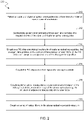
FIG. 2 shows features of a method to facilitate optical coupling between a PIC chip and a waveguide according to an embodiment. -
FIG. 3 shows a perspective view of an assembly to provide optical coupling between a PIC and a waveguide according to an embodiment. -
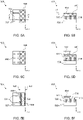
FIGs. 4A, 4B show features of respective PICs each according to a corresponding embodiment. -
FIGs. 5A through 5F show cross-sectional views each of a respective stage of processing to provide cylindrical lenses of a PIC according to an embodiment. -
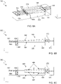
FIGs. 6A through 6C show respective views each of a respective assembly to optically couple a PIC and waveguide according to a corresponding embodiment. -
FIG. 7A shows an exploded view of an assembly to optically couple a PIC to a waveguide according to an embodiment. -
FIG. 7B shows, in a cross-sectional top view, structures of the assembly represented inFIG. 7A . -
FIGs. 8A, 8B show features of respective assemblies each to optically couple a PIC to optical fibers via a waveguide according to a corresponding embodiment. -
FIG. 9 shows a perspective view of an assembly to provide optical coupling between an integrated waveguide structure of a PIC and an optical fiber array according to an embodiment. -
FIG. 10 is a functional block diagram illustrating a computing device in accordance with one embodiment. -
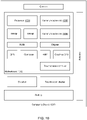
FIG. 11 is a functional block diagram illustrating an exemplary computer system, in accordance with one embodiment. -
FIG. 12 is a cross-sectional view of an interposer implementing one or more embodiments. - Embodiments discussed herein variously provide techniques and mechanisms for coupling a lens structure of a photonic integrated circuit (PIC) chip to an optical fiber via a waveguide which is distinct from the PIC. The technologies described herein may be implemented in one or more electronic devices. Non-limiting examples of electronic devices that may utilize the technologies described herein include any kind of mobile device and/or stationary device, such as cameras, cell phones, computer terminals, desktop computers, electronic readers, facsimile machines, kiosks, laptop computers, netbook computers, notebook computers, internet devices, payment terminals, personal digital assistants, media players and/or recorders, servers (e.g., blade server, rack mount server, combinations thereof, etc.), set-top boxes, smart phones, tablet personal computers, ultra-mobile personal computers, wired telephones, combinations thereof, and the like. More generally, the technologies described herein may be employed in any of a variety of electronic devices including a PIC which is coupled to a substrate to accommodate optical coupling, via a waveguide, between an optical fiber and a cylindrical lens formed at an edge of the PIC.
- In the following description, numerous details are discussed to provide a more thorough explanation of the embodiments of the present disclosure. It will be apparent to one skilled in the art, however, that embodiments of the present disclosure may be practiced without these specific details. In other instances, well-known structures and devices are shown in block diagram form, rather than in detail, in order to avoid obscuring embodiments of the present disclosure.
- Note that in the corresponding drawings of the embodiments, signals are represented with lines. Some lines may be thicker, to indicate a greater number of constituent signal paths, and/or have arrows at one or more ends, to indicate a direction of information flow. Such indications are not intended to be limiting. Rather, the lines are used in connection with one or more exemplary embodiments to facilitate easier understanding of a circuit or a logical unit. Any represented signal, as dictated by design needs or preferences, may actually comprise one or more signals that may travel in either direction and may be implemented with any suitable type of signal scheme.
- Throughout the specification, and in the claims, the term "connected" means a direct connection, such as electrical, mechanical, or magnetic connection between the things that are connected, without any intermediary devices. The term "coupled" means a direct or indirect connection, such as a direct electrical, mechanical, or magnetic connection between the things that are connected or an indirect connection, through one or more passive or active intermediary devices. The term "circuit" or "module" may refer to one or more passive and/or active components that are arranged to cooperate with one another to provide a desired function. The term "signal" may refer to at least one current signal, voltage signal, magnetic signal, or data/clock signal. The meaning of "a," "an," and "the" include plural references. The meaning of "in" includes "in" and "on."
- The term "device" may generally refer to an apparatus according to the context of the usage of that term. For example, a device may refer to a stack of layers or structures, a single structure or layer, a connection of various structures having active and/or passive elements, etc. Generally, a device is a three-dimensional structure with a plane along the x-y direction and a height along the z direction of an x-y-z Cartesian coordinate system. The plane of the device may also be the plane of an apparatus which comprises the device.
- The term "scaling" generally refers to converting a design (schematic and layout) from one process technology to another process technology and subsequently being reduced in layout area. The term "scaling" generally also refers to downsizing layout and devices within the same technology node. The term "scaling" may also refer to adjusting (e.g., slowing down or speeding up - i.e. scaling down, or scaling up respectively) of a signal frequency relative to another parameter, for example, power supply level.
- The terms "substantially," "close," "approximately," "near," and "about," generally refer to being within +/- 10% of a target value. For example, unless otherwise specified in the explicit context of their use, the terms "substantially equal," "about equal" and "approximately equal" mean that there is no more than incidental variation between among things so described. In the art, such variation is typically no more than +/-10% of a predetermined target value.
- It is to be understood that the terms so used are interchangeable under appropriate circumstances such that the embodiments of the invention described herein are, for example, capable of operation in other orientations than those illustrated or otherwise described herein.
- Unless otherwise specified the use of the ordinal adjectives "first," "second," and "third," etc., to describe a common object, merely indicate that different instances of like objects are being referred to and are not intended to imply that the objects so described must be in a given sequence, either temporally, spatially, in ranking or in any other manner.
- The terms "left," "right," "front," "back," "top," "bottom," "over," "under," and the like in the description and in the claims, if any, are used for descriptive purposes and not necessarily for describing permanent relative positions. For example, the terms "over," "under," "front side," "back side," "top," "bottom," "over," "under," and "on" as used herein refer to a relative position of one component, structure, or material with respect to other referenced components, structures or materials within a device, where such physical relationships are noteworthy. These terms are employed herein for descriptive purposes only and predominantly within the context of a device z-axis and therefore may be relative to an orientation of a device. Hence, a first material "over" a second material in the context of a figure provided herein may also be "under" the second material if the device is oriented upside-down relative to the context of the figure provided. In the context of materials, one material disposed over or under another may be directly in contact or may have one or more intervening materials. Moreover, one material disposed between two materials may be directly in contact with the two layers or may have one or more intervening layers. In contrast, a first material "on" a second material is in direct contact with that second material. Similar distinctions are to be made in the context of component assemblies.
- The term "between" may be employed in the context of the z-axis, x-axis or y-axis of a device. A material that is between two other materials may be in contact with one or both of those materials, or it may be separated from both of the other two materials by one or more intervening materials. A material "between" two other materials may therefore be in contact with either of the other two materials, or it may be coupled to the other two materials through an intervening material. A device that is between two other devices may be directly connected to one or both of those devices, or it may be separated from both of the other two devices by one or more intervening devices.
- As used throughout this description, and in the claims, a list of items joined by the term "at least one of' or "one or more of' can mean any combination of the listed terms. For example, the phrase "at least one of A, B or C" can mean A; B; C; A and B; A and C; B and C; or A, B and C. It is pointed out that those elements of a figure having the same reference numbers (or names) as the elements of any other figure can operate or function in any manner similar to that described, but are not limited to such.
- In addition, the various elements of combinatorial logic and sequential logic discussed in the present disclosure may pertain both to physical structures (such as AND gates, OR gates, or XOR gates), or to synthesized or otherwise optimized collections of devices implementing the logical structures that are Boolean equivalents of the logic under discussion.
- Embodiments described herein variously facilitate the provisioning of an assembly which comprises a substrate and a photonic integrated circuit (PIC) chip coupled thereto, wherein an optical waveguide structure is adjacent and optically coupled to photonic structures formed by the PIC chip. More particularly, the PIC chip forms one or more integrated optical structures - referred to herein as integrated edge-oriented couplers (IECs) - which are configured to be optically coupled for horizontal signal communication with the optical waveguide structure. In this particular context, "horizontal" refers to a direction in parallel with a plane in which one of two opposite sides of a PIC chip extends (e.g., wherein an edge of the PIC chip extends between the two sides). In various embodiments, an arrangement of the optical waveguide structure and one or more IECs facilitates the communication of an optical signal - in a direction parallel to a side of the PIC chip - between an IEC and a corresponding optical fiber. In various embodiments, a planar optical waveguide structure enables beam expansion, mode conversion, and/or other functionality to facilitate photonic signal communication between IECs of a PIC chip and another device (such as a fiber array) which is optically coupled to said PIC chip.
- In providing such an assembly, some embodiments variously improve the ease, efficiency and accuracy with which a PIC chip is optically coupled to an array of optical fibers (and/or to another PIC chip, for example). Additionally or alternatively, such embodiments efficiently provide a low (z-dimension) profile solution for communicating optical signals to and/or from a packaged device.
- Certain features of various embodiments are described herein with reference to an assembly comprising a PIC chip, and a preformed optical waveguide structure (referred to herein as an "waveguide preform") which are variously adhered, connected or otherwise coupled - directly or indirectly - each to a substrate. The PIC chip and the optical waveguide preform are distinct from each other, and extend over different respective regions of a package substrate (or other suitable substrate).
- In other embodiments, a PIC chip comprises both a plurality of IECs and an integrated optical waveguide structure which is optically coupled to said plurality of IECs. In one such embodiment, a PIC chip is of a silicon on insulator (SOI) type - e.g., comprising an upper layer of a semiconductor material, an underlayer which, for example, comprises the same (or another) semiconductor material, and a layer of a buried oxide between the upper layer and the underlayer. The upper layer comprises silicon and/or the buried oxide comprises silicon dioxide, for example. By way of illustration and not limitation, the integrated optical waveguide structure is deposited, nano-imprinted and/or otherwise formed on a region of the buried oxide which, for example, was previously exposed by removal of a portion of the upper layer.
- Certain features of various embodiments are described herein with reference to a given IEC of a PIC chip forming a divergent lens surface. In this particular context, "divergent" refers to the characteristic of the lens surface extending out from - e.g., as opposed to recessing into - a given edge (or other) surface of a PIC chip. In one illustrative embodiment, a divergent lens surface comprises a continuous convex surface at an edge of a PIC chip. Alternatively, a divergent lens surface comprises a plurality of discrete facets, individual ones of which are each substantially flat - e.g., over a respective transverse length and a respective longitudinal height of the lens surface. In one such embodiment, the plurality of discrete facets are "piecewise convex" - e.g., wherein corners (or other such structures) formed by said facets are variously located along the same convex curve.
-
FIG. 1A shows features of adevice 100 to facilitate optical signal communication between a photonic integrated circuit (PIC) chip and an optical fiber according to an embodiment.FIG. 1B shows aperspective view 101 of selected structures ofdevice 100.Device 100 illustrates one example of an embodiment wherein a PIC chip is coupled to a substrate to accommodate edge-wise optical coupling, via a waveguide structure (in this case, a waveguide preform), to one or more optical fibers. - As variously shown in
FIGs. 1A, 1B ,device 100 comprises asubstrate 110 and aPIC chip 130 coupled thereto.Substrate 110 comprises any of various organic, glass, silicon or other suitable substrate materials that (for example) are adapted from conventional packaging techniques. In one such embodiment,substrate 110 functions as a package substrate which is to provide support forPIC chip 130, an optical waveguide structure, and (for example) one or more other integrated circuit (IC) chips - e.g., including theillustrative IC chip 120 shown. By way of illustration and not limitation,PIC 130 andIC chip 120 are variously coupled to thesubstrate 110 via respective ones ofconductive contacts 112, which (for example) are disposed in any of various suitable underfill materials. Theconductive contacts 112 comprise any type of structure and materials - whether disposed in multiple layers or combined to form one or more alloys and/or one or more intermetallic compounds - capable of providing electrical communication betweensubstrate 110 and one or more chips including (in this example embodiment)IC chip 120 andPIC chip 130. For example,conductive contacts 112 include copper, aluminum, gold, silver, nickel, titanium, tungsten, as well as any combination of these and/or other metals. - In an embodiment, each of conductive contacts 112 (e.g., a pad, bump, stud bump, column, pillar, or other suitable structure or combination of structures) couples to a corresponding electrically conductive terminal (e.g., a pad, bump, stud bump, column, pillar, or other suitable structure or combination of structures) on a respective chip. Solder (e.g., in the form of balls or bumps) is disposed on the
conductive contacts 112 or on terminals of a given chip, which are then used to join PIC chip 130 (and, for example, IC chip 120) to substrate 110 - e.g., using a solder reflow process. In some embodiments, the solder material comprises any one or more of tin, copper, silver, gold, lead, nickel, indium, as well as any combination of these and/or other metals. In one such embodiment, the solder also includes one or more additives and/or filler materials to alter a characteristic of the solder (e.g., to alter the reflow temperature). Of course, it should be understood that many other types of interconnects and materials are possible (e.g., wirebonds extending betweensubstrate 110 and one ofIC chip 120 or PIC chip 130).Device 100 further comprises aball grid array 114 positioned proximate a surface of thesubstrate 110 to provide electrical connections with an underlying device (not shown) - e.g., a printed circuit board. - The one or more IC chips illustrated by
IC chip 120 comprise (for example) any of a variety of integrated circuit devices which are suitable for a particular application, such as (but not limited to) a microprocessor, a graphics processor, a signal processor, a network processor, a chipset, etc. In one embodiment,IC chip 120 comprises a system-on-chip (SoC) comprising one or more functional units (e.g., one or more processing units, one or more graphics units, one or more communications units, one or more signal processing units, one or more security units, etc.). However, it should be understood that some disclosed embodiments are not limited to any particular type or class of functionality to be provided with IC chip 120 (or other such integrated circuitry coupled tosubstrate 110 and PIC chip 130). -
PIC chip 130 comprises one or more optical coupler structures - e.g., including the illustrative integrated edge-oriented couplers (IECs) 136 shown - which are formed at anedge 135 ofPIC chip 130.PIC 130 further comprises integratedcircuitry 132 which, for example, comprises optical signal transit circuitry and/or optical signal receiver circuitry. For example, integrated circuitry 132 - e.g., comprising any of a various lasers, modulators, photodetectors and/or other integrated photonics circuits - is formed on anactive side 131 ofPIC chip 130, wherein anopposite side 133 comprises terminals with whichPIC chip 130 is to variously communicate electrical signals (for example, withIC chip 120 and/or other circuitry via substrate 110). In some embodiments, one or more optical signal transit circuits and/or one or more optical signal receiver circuits ofintegrated circuitry 132 are optically coupled each to a respective one of IECs 136 - e.g., via a corresponding one of one or more photonic waveguides of PIC chip 130 (such as the illustrativephotonic waveguides 134 shown). - In an example embodiment, a semiconductor substrate of
PIC chip 130 is of a silicon on insulator (SOI) type, and comprises (for example) an upper layer of a semiconductor material comprising silicon, an underlayer of the same semiconductor material (or another semiconductor material), and a buried oxide (BOX) layer between the upper layer and the underlayer.Photonic waveguides 134 and/orIECs 136 comprise any of various materials (such as crystalline silicon) which are suitable to communicate an optical signal - e.g., wherein such materials are adapted from conventional PIC chip designs. - To facilitate edge-wise communication of one or more optical signals to and/or from PIC chip 130 - i.e., via edge 135 -
device 100 further comprises a planaroptical waveguide preform 140 which is adhered to, or otherwise coupled over, a second region ofsubstrate 110. In an embodiment, anedge 141 of waveguide preform 140 - which comprisescladdings core 144 therebetween - is adjacent to IECs 136 atedge 135. In the example embodiment shown,device 100 further comprises (or facilitates coupling to) afiber array housing 150 which hasoptical fibers 152 extending therein. By way of illustration and not limitation,device 100 supports coupling to a pluggable connector of an optical cable - e.g., wherein the connector includesfiber array housing 150, and whereinoptical fibers 152 of the cable extend fromdevice 100 to couple to a remote packaged, or other, device (not shown). Although some embodiments are not limited in this regard, respective distal ends of some or all ofoptical fibers 152 variously form (or are coupled to)lens structures 154 to facilitate optical coupling with anadjacent edge 145 ofwaveguide preform 140. - In various embodiments,
waveguide preform 140 is formed by processing which, for example, is adapted from conventional photonics fabrication techniques. By way of illustration and not limitation,core 144 comprises any of various light transmissive materials - such as silicon nitride (Si3N4), silicon oxynitride (SiOxNy), and/or any of a various suitable doped oxides - exhibiting refractive index characteristics which facilitate optical coupling with optical fiber materials. However, it is to be appreciated that some embodiments are not limited to a particular one or more materials ofwaveguide preform 140, and the such materials may differ in various embodiments according to implementation-specific details. As described herein, one or more surfaces of waveguide preform 140 (in some embodiments) are etched, laser ablated or otherwise shaped to form any of various recess structures therein - e.g., wherein one or more such recess structures are each to facilitate optical interfacing betweenwaveguide preform 140 and a respective IEC or a respective optical fiber. - In some embodiments,
photonic waveguides 134 are coplanar with each other - e.g., wherein the plurality ofphotonic waveguides 134 each extend in an x-y plane such as one at (or under) aside 131 ofPIC chip 130. For example, some or all ofphotonic waveguides 134 are each within a thickness of material in or on a semiconductor substrate of PIC chip 130 - e.g., whereinphotonic waveguides 134 are within a top portion of the semiconductor substrate. In one such embodiment, some or all ofIECs 136 are coplanar with each other - e.g., whereinIECs 136 each extend in an x-y plane such as one at (or under)side 131. -
IECs 136 each terminate a respective one ofphotonic waveguides 134, and each form a respective lens surface that is divergent (in a y-z plane) and, in some embodiments, is substantially flat (in a x-y plane) over at least a thickness of the semiconductor substrate ofPIC chip 130. For example,IECs 136 are each substantially flat atside 131, in some embodiments. - In the example embodiment shown,
IECs 136 variously extend from an otherwise flat (in an y-z plane) side 135 - e.g., whereinIECs 136 form a portion ofedge 135 which is positioned farthest along the x-axis in the direction ofwaveguide preform 140. In an alternative embodiment, edge 135 forms a stepped structure, wherein an upper (along the z-axis) portion of the stepped structure comprisesIECs 136, and wherein a lower (along the z-axis) portion of the stepped structure extends past IECs 136 - e.g., by at least as much as a (x-axis) depth of a curvature of one of IECs 136 - to provide mechanical support for an overlapping portion ofwaveguide preform 140 - In some embodiments, a given one of
IECs 136 forms a convex lens surface which is substantially semicylindrical - e.g., wherein a curvature of the convex lens surface is symmetrical about a primary axis (along the x-dimension) of the convex lens surface. In one such embodiment, the primary axis of the given convex lens surface is in a lateral (y-axis) alignment with an optical axis of a corresponding one of the photonic waveguides 134 - e.g., wherein a radius of curvature of the given convex lens surface is equal to or larger than one half of a (y-axis) width of the corresponding photonic waveguide. - Additionally or alternatively, a divergent lens surface of one of
IECs 136 comprises a plurality of discrete diffractive edge facets which are symmetrically distributed about a primary axis of said divergent lens surface. In one such embodiment, individual ones of the edge facets are substantially flat over a transverse (y-axis) length and a longitudinal (z-axis) height of the lens surface. - In some embodiments, one or more divergent lens surfaces of
IECs 136 each extend into a semiconductor substrate ofPIC chip 130. By way of illustration and not limitation,photonic waveguides 134 andIECs 136 each comprise a material including silicon. In one such embodiment, the semiconductor substrate ofPIC chip 130 is of a silicon-on-insulator (SOI) type - e.g., whereinPIC chip 130 comprises a layer of silicon dioxide between the material and an underlayer. For example, one or more divergent lens surfaces ofIECs 136 each stop at, or within, the layer of silicon dioxide. Additionally or alternatively, one or more divergent lens surfaces ofIECs 136 each extend at least partially through the underlayer. - In the example embodiment shown,
core 144 forms a portion ofedge 141 which is substantially flat (for example, in a y-z plane) across some or all ofIECs 136. In some alternative embodiments, edge 141 forms one or more surface recesses which are each to at least partially receive or otherwise interface with a corresponding one ofIECs 136. For example, in one such embodiment, some or all of said surface recesses each have a respective profile which is complementary to the profile of a divergent lens surface formed by a corresponding one ofIECs 136. By way of illustration and not limitation, one or more divergent lens surfaces ofIECs 136 are each semicylindrical and convex, where one or more surface recesses atedge 141 each comprises a concave semicylinder. Some or all recesses formed atedge 141, in some embodiments, extend through an entire (z-axis) thickness ofcore 144 and ofcladding 146. Additionally or alternatively, some or all such recesses atedge 141 each form a respective surface which is substantially flat (in a x-y plane) over at least a partial thickness ofcore 144. - In the example embodiment shown, another
edge 145 of waveguide preform 140 - theedge 145 opposite edge 141 - is substantially flat (for example, in a y-z plane) across some or all ofIECs 136. In some other embodiments,edge 145 alternatively forms one or more surface recesses which are each to at least partially receive or otherwise interface with a corresponding one of optical fibers 152 (for example, to a corresponding one of lens structures 154). For example, in one such embodiment, edge 145 forms one or more substantially semispherical recesses, whereincore 144 optically couples individual ones ofIECs 136 each to a corresponding one of said one or more semispherical recesses. For example,fiber array housing 150 is connected to, adhered to and/or otherwise disposed over a third region ofsubstrate 110, wherein individual ones of optical fibers 152 (and, for example, individual ones of lens structures 154) are to be received by, or otherwise optically coupled to, individual ones of the second plurality of concave lens surfaces. - Although
FIGs. 1A, 1B show device 100 as providing optical coupling betweenIECs 136 ofPIC chip 130 andoptical fibers 152, it is to be appreciated that planar optical waveguide preform 140 (or any of various other planar optical waveguide structures having features described herein) additionally or alternatively supports optical coupling between IECs of a PIC chip, and any of various other external photonic devices (such as another PIC chip), in different embodiments. For example, some embodiments are variously provided entirely by a PIC chip, or entirely by a packaged device which includes such a PIC chip (e.g., independent of whether a PIC chip of said packaged device is optically coupled to another device via a planar optical waveguide structure of said packaged device). -
FIG. 2 shows features of amethod 200 to facilitate optical coupling of a PIC chip to a waveguide according to an embodiment. Operations such as those ofmethod 200 are performed, for example, to provide structures ofdevice 100. - As shown in
FIG. 2 ,method 200 comprises (at 210) patterning a plurality of coplanar optical waveguides into a thickness of a material over a plane of a substrate. In one illustrative embodiment, a silicon-on-insulator (SOI) substrate comprises an upper layer, an underlayer, and a buried dielectric (e.g. oxide) layer disposed therebetween. The upper layer (and, in some embodiments, the underlayer) comprises crystalline silicon and/or any of various other materials suitable to communicate an optical signal. In one such embodiment, the upper layer is then etched and/or otherwise patterned to form one or more rib waveguide structures therein or thereon. The patterning at 210 involves, for example, wet or dry etching techniques, any of various lithographic processes, or other patterning processes such as ablation, ruling, or other techniques which will be apparent to those skilled in the art. -
Method 200 further comprises (at 212) subtractively patterning divergent lens profiles each at a terminus of a respective one of the plurality of coplanar optical waveguides. By way of illustration and not limitation, the subtractive patterning comprises deposition of a patterned mask over a region of the substrate where the plurality of coplanar optical waveguides are to end (and, for example, where an edge of a PIC chip is to be subsequently formed). Subsequently, deep reactive ion etching (DRIE) and/or other suitable etch processing is performed through the patterned mask to form one or more lens structures. In some embodiments the patterning at 210 is performed concurrently with the subtractive patterning at 212. -
Method 200 further comprises (at 214) singulating a photonic integrated circuit (PIC) chip comprising the plurality of coplanar optical waveguides, the divergent lens profiles, and a portion of the substrate. For example, the singulating at 214 comprises dicing a semiconductor wafer to form the edges of the PIC chip, wherein one such edge comprises integrated edge-oriented couplers (IECs) which each include a respective lens structure formed at 212. In some embodiments,method 200 additionally or alternatively comprises operations (not shown) to form a planar optical waveguide structure which is integrated on the substrate - e.g., wherein a core of the planar optical waveguide structure is adjacent to (and optically coupled with) the IECs, and wherein the planar optical waveguide structure is integrated with, and extends to an edge of, the singulated PIC chip. -
Method 200 further comprises (at 216) coupling the PIC chip over a first region of a package substrate - e.g., wherein such coupling comprises operations adapted from conventional flip-chip, wire bonding and/or other techniques.Method 200 further comprises (at 218) coupling an optical waveguide preform over a second region of the package substrate - e.g., wherein the waveguide preform is adhered or otherwise bonded to the second region. In other embodiments,method 200 omits the coupling at 218 - e.g., wherein the planar optical waveguide structure is formed as an integrated structure of the PIC chip.Method 200 further comprises (at 220) coupling an array of optical fibers to the planar optical waveguide preform. In an embodiment, the waveguide preform comprises a core, opposite ends of which are optically coupled (respectively) to the IECs and to the array of optical fibers. -
FIG. 3 shows features of anassembly 300 to facilitate optical communications with a PIC chip and a waveguide according to an embodiment. In various embodiments,assembly 300 provides functionality such as that of device 100 - e.g., wherein one or more operations ofmethod 200 are to provide structures ofassembly 300. - As shown in
FIG. 3 ,assembly 300 comprises aPIC chip 330, afiber array housing 350, and awaveguide preform 340 which are variously coupled, directly or indirectly, to a substrate (not shown) such assubstrate 110.Waveguide preform 340 facilitates edge-wise communication of one or more optical signals to and/or from PIC chip - e.g., wherein acore 344 ofwaveguide preform 340 optically couplesoptical fibers fiber array housing 350, each to a respective one of IECs 336a, 336b which are variously formed at an edge ofPIC chip 330. In one such embodiment,PIC chip 330,waveguide preform 340, andfiber array housing 350 correspond functionally toPIC chip 130,waveguide preform 140, and fiber array housing 150 (respectively) - e.g., wherein IECs 336a, 336b,core 344, andoptical fibers IECs 136,core 144, and optical fibers 152 (respectively). - In the example embodiment shown, a length x2 of
core 344, between the edge ofPIC chip 330 andfiber array housing 350, is in a range of 0.5 mm to 100 mm - e.g., wherein length x2 is in a range of 1.0 mm to 50mm (and, in some embodiments, in a range of 1.0 mm to 10mm). In one such embodiment, an x-axis depth x1 of a curvature ofIEC 336a (for example) is in a range of 3 µm to 50 µm - e.g., wherein depth x1 is in a range of 4 µm to 20 µm and, in some embodiments, in a range of 5 µm to 15 µm. By way of illustration and not limitation, a y-axis width y1 of a given one of IECs 336a, 336b is in a range of 20 µm to 200 µm (e.g., in a range of 20 µm to 100 µm and, in some embodiments, in a range of 20 µm to 50 µm). In one such embodiment,IEC 336a forms a convex surface, wherein a radius of curvature r1 of the convex surface is at least 50% of width y1 (e.g., where radius r1 is in a range of 50% to 150% of width y1). - In the example embodiment shown,
core 344 has a (z-axis) thickness z1 which is the same along the length x2. For example, thickness z1 is in a range of 0.1 microns (µm) to 20 µm (e.g., in a range of 3 µm to 10 µm). In some alternative embodiments,core 344 has different thicknesses at various points along the length x2. In one such embodiment, a first end ofcore 344, which adjoinsIECs core 344, which adjoinsoptical fibers fiber array housing 350, is in a range of 30 µm to 200 µm. It is appreciated that, in some embodiments, the above described ranges of values for various dimensions ofassembly 300 are merely illustrative, and that some or all such ranges may differ in other embodiments, according to implementation-specific details. -
FIGs. 4A, 4B show features ofrespective PIC chips method 200 are to facilitate optical coupling of a waveguide preform with one ofPIC chips - As shown in
FIG. 4A , asurface 431 ofPIC chip 430 has formed therein or thereonsilicon waveguides surface 431. Anedge 435 ofPIC chip 430 forms the respective divergent lens surfaces of IECs 436a, 436b, 436c, which are each at a respective terminus of a corresponding one ofsilicon waveguides PIC chip 430 provides functionality of PIC chip 130 - e.g., whereinsilicon waveguides edge 435, andIECs photonic waveguides 134,edge 135, and IECs 136 (respectively). -
PIC chip 430 illustrates one embodiment wherein one or more IECs each form a respective divergent lens surface which is piecewise convex. For example, the divergent lens surface ofIEC 436c comprises a plurality of discretediffractive edge facets 438 which, in some embodiments, are symmetrically distributed about a primary axis CL1 ofIEC 436c. In one such embodiment, individual ones of saidedge facets 438 are each substantially flat over a transverse (y-axis) length and a longitudinal (z-axis) height ofIEC 436c. Additionally or alternatively, the primary axis CL1 ofIEC 436c is in a transverse (y-axis) alignment with an optical axis of the correspondingsilicon waveguide 434c. In one such embodiment, the divergent lens surface ofIEC 436c includes corners (or other such points) which are distributed along a semicylindrical curve, a radius of which is equal to or larger than one half of a (y-axis) width w1 ofsilicon waveguide 434c. - As shown in
FIG. 4B , asurface 481 ofPIC chip 480 has formed therein or thereonsilicon waveguides surface 481. Anedge 485 ofPIC chip 480 forms the respective divergent lens surfaces of IECs 486a, 486b, 486c, at the respective termini ofsilicon waveguides PIC chip 480 provides functionality of PIC chip 130 - e.g., whereinsilicon waveguides edge 485, andIECs photonic waveguides 134,edge 135, and IECs 136 (respectively). -
PIC chip 480 illustrates one embodiment wherein one or more IECs each form a respective convex lens surface. For example,IEC 486a forms a convex lens surface which is symmetrical about a primary axis CL2. In one such embodiment, the primary axis CL2 ofIEC 486a is in a transverse (y-axis) alignment with an optical axis of the correspondingsilicon waveguide 484a. Additionally or alternatively, the convex surface ofIEC 486a conforms to a semicylindrical curve, a radius of which is equal to or larger than one half of a (y-axis) width w2 ofsilicon waveguide 484a. -
FIGs. 5A, 5C, 5E show various structures duringrespective stages stages PIC chips method 200 include or are otherwise based on some or all such processing. The various structures instages cross-sectional side views FIGs. 5B, 5D, 5F (respectively). The cross-sections forside views - As shown in
FIG. 5A , structures atstage 500 are formed by processing of a SOI wafer which comprises anunderlayer 539 of a semiconductor material, aninsulator layer 538 comprising any of various suitable dielectric materials (such as SiO2) overunderlayer 539, and anupper layer 537 of a material which (for example) comprises silicon. Some or all of upper layer 537 (and, in some embodiments, the underlayer 539) comprises crystalline silicon and/or any of various other materials suitable to communicate an optical signal. - At
stage 500, photonic waveguide structures (such as theillustrative silicon waveguides 534 shown) are formed in or on layer 537 - e.g., where such forming includes any of various suitable wet or dry etching techniques, any of various lithographic processes, or other patterning processes such as ablation, ruling, or the like. In one such embodiment,silicon waveguides 534 are rib waveguide structures formed by patterned etching of crystalline silicon in a material layer above a horizontal (x-y) plane p1 which extends in or onlayer 537.Silicon waveguides 534 variously extend to a body of a material 540 which (for example) comprises crystalline silicon or any of various other materials which are suitable to communicate an optical signal. At stage 500 (or alternatively, at a later processing stage),silicon waveguides 534 further extend variously betweenmaterial 540 and integrated circuitry (not shown) - e.g., including integrated photonic circuitry and, in some embodiments, integrated electrical circuitry - which is formed in or onlayer 537. In various embodiments,material 540 has a same composition as a material ofsilicon waveguides 534. - As shown in
FIG. 5C , apatterned mask 550 is formed atstage 502 on structures which are variously formed in or on layer 537 - e.g., the structures includingsilicon waveguides 534, and portions ofmaterial 540. In an embodiment, some portions of patterned mask 550 - which extend over material 540 - comprise various concave or otherwise divergent profiles, which are to facilitate the formation of IEC structures. - As shown in
FIG. 5E , structures atstage 504 are formed by an etch process, after which the patternedmask 550 is removed fromsilicon waveguides 534 and/or from other structures which are formed in or onlayer 537. In some embodiments, the etch process - e.g., comprising deep reactive ion etching (DRIE) - selectively removes portions ofmaterial 540, wherein remaining portions ofmaterial 540form IECs 536 which are at an edge portion oflayer 537, and which are each at a respective termini of a corresponding one ofsilicon waveguides 534. - In this example embodiment,
IECs 536 extend vertically to insulator layer 538 - e.g., wherein the etch process exposes asurface 543 of insulator layer 538 (for example).IECs 536 forms one or more divergent lens profiles, wherein a maximum horizontal (x-axis) extent of said lens profiles is indicated by the vertical plane 542 (i.e., an y-z plane) shown. In various embodiments, subsequent singulation forms a PIC chip which comprises the structures shown inview 505. For example, an edge of the singulated PIC chip forms a stepped structure comprising an upper portion and a lower portion. In one such embodiment, the upper portion, which is abovesurface 543, comprises the respective divergent lens profiles of IECs 536 - e.g., wherein the lower portion is belowsurface 543, and extends horizontally pastvertical plane 542 to anothervertical plane 541. As described herein, the lower portion provides support for, and/or facilitates alignment with, a waveguide preform that is to be optically coupled withIECs 536, in some embodiments. -
FIGs. 6A through 6C show features ofrespective assemblies Assemblies assemblies device 100, or assembly 300 (for example) - e.g., whereinmethod 200 is to provide functionality of one or more ofassemblies - As shown in
FIG. 6A ,assembly 600 comprises aPIC chip 630, afiber array housing 650, and awaveguide preform 640 which optically couples optical fibers 652 (which extend in fiber array housing 650) each to a respective one ofIECs 636 which are variously formed at anedge 635 ofPIC chip 630.IECs 636 facilitate edge-wise communication of optical signals - viasilicon waveguides 634 of PIC chip 630 - betweenwaveguide preform 640 and integrated circuitry ofPIC chip 630. For example,waveguide preform 640 comprises cladding 642, cladding 646, and acore 644 which is extends therebetween, wherein a first edge ofwaveguide preform 640 is positioned to have one end ofcore 644 be adjacent to IECs 636 (which are each at a terminus of a respective one of silicon waveguides 634). A second edge of waveguide preform 640 (opposite the first edge) is positioned to have an opposite end ofcore 644 be adjacent tooptical fibers 652 which variously extend infiber array housing 650. - In one such embodiment,
PIC chip 630,waveguide preform 640, andfiber array housing 650 correspond functionally toPIC chip 130,waveguide preform 140, and fiber array housing 150 (respectively) - e.g., whereinsilicon waveguides 634,edge 635,IECs 636, cladding 642,core 644, cladding 646, andoptical fibers 652 correspond functionally tophotonic waveguides 134,edge 135,IECs 136, cladding 142,core 144, cladding 146, and optical fibers 152 (respectively). - In the example embodiment shown, the top and bottom surfaces of
core 644 are variously inclined each with respect to a horizontal (x-y) plane in whichsilicon waveguides 634 variously extend. Accordingly,core 644 provides for an expansion of an optical signal during communication thereof from one ofIECs 636 to a corresponding one ofoptical fibers 652. Alternatively or in addition,core 644 provides for an optical signal decreasing in size during communication thereof from one ofoptical fibers 652 to a corresponding one ofIECs 636. - Additionally or alternatively, in some embodiments,
edge 635 ofPIC chip 630 forms a stepped structure, wherein an upper portion of the stepped structure comprisesIECs 636, and a lower portion of the stepped structure extendspast IECs 636. In one such embodiment,waveguide preform 640 overlaps the lower portion of said stepped structure - e.g., wherein the lower portion facilitates alignment of, and/or provides support for, at least a portion ofwaveguide preform 640. - As shown in
FIG. 6B ,assembly 660 comprises aPIC chip 661, afiber array housing 670, and awaveguide preform 665 which optically couples optical fibers 672 (which extend in fiber array housing 670) each to a respective one ofIECs 664 which are variously formed at anedge 663 ofPIC chip 661.IECs 664 facilitate edge-wise communication of optical signals - viasilicon waveguides 662 of PIC chip 661 - betweenwaveguide preform 665 and integrated circuitry ofPIC chip 661. In one suchembodiment PIC chip 661,waveguide preform 665, andfiber array housing 670 correspond functionally toPIC chip 130,waveguide preform 140, and fiber array housing 150 (respectively). In the example embodiment shown, a core of waveguide preform 665 (the core adjacent to IECs 664 and optical fibers 672) comprises atop surface 666 and abottom surface 667, only one of which is inclined with respect to a horizontal (x-y) plane in whichsilicon waveguides 662 variously extend. For example,top surface 666 is inclined toward atop side 668 ofwaveguide preform 665, whilebottom surface 667 is parallel to bothtop side 668 and abottom side 669 ofwaveguide preform 665. - As shown in
FIG. 6C ,assembly 680 comprises aPIC chip 681, afiber array housing 690, and awaveguide preform 685 which optically couples optical fibers 692 (which extend in fiber array housing 690) each to a respective one ofIECs 684 which are variously formed at anedge 683 ofPIC chip 681.IECs 684 facilitate communication of optical signals, viasilicon waveguides 682 ofPIC chip 681, betweenwaveguide preform 685 and integrated circuitry ofPIC chip 681. In one suchembodiment PIC chip 681,waveguide preform 685, andfiber array housing 690 correspond functionally toPIC chip 130,waveguide preform 140, and fiber array housing 150 (respectively). In the example embodiment shown, a core of waveguide preform 685 (the core adjacent to IECs 684 and optical fibers 692) comprises atop surface 686 and abottom surface 687, which are variously inclined step-wise in different respective vertical (z-axis) directions, along the length ofwaveguide 685, fromIECs 684 tooptical fibers 692. -
FIG. 7A shows, in an exploded view, features of anassembly 700 to communicate an optical signal with a PIC chip according to an embodiment.FIG. 7B shows a cross-sectionaltop view 701 ofassembly 700. In various embodiments,assembly 700 includes some or all features of device 100 - e.g., wherein structures ofassembly 700 are provided by and/or used in operations ofmethod 200, for example. - As shown in
FIG. 7A ,assembly 700 comprises aPIC chip 730, awaveguide preform 740, and afiber array housing 750 which, for example, correspond functionally toPIC chip 130,waveguide preform 140, and fiber array housing 150 (respectively). In one such embodiment,IECs 736, which are formed by anedge 735 ofPIC chip 730, facilitate edge-wise communication of optical signals betweenwaveguide preform 740 and integrated circuitry (not shown) ofPIC chip 730. For example,waveguide preform 740 comprises cladding 742, cladding 746, and acore 744 which is extends therebetween, wherein anedge 741 ofwaveguide preform 740 is positioned to have one end ofcore 744 be adjacent to edge 735. Anotheredge 745 ofwaveguide preform 740 is positioned to have an opposite end ofcore 744 be adjacent to anedge 755 offiber array housing 750. In an embodiment,optical fibers 752 extending fromedge 755 are optically coupled, viacore 744, each to a corresponding one ofIECs 736. - In the example embodiment shown, edge 741
forms recess structures 743, individual ones of which are each to receive, or otherwise interface with, a corresponding one ofIECs 736. For example, individual ones ofrecess structures 743 each have a respective profile which is complementary to a profile of the divergent lens surface of the corresponding IEC. In some embodiments, some or all ofrecess structures 743 extend only partially along the (z-axis) height of edge 741 - e.g., wherein individual ones ofrecess structures 743 each form a substantially flat, horizontal (in an x-y plane) surface over at least a partial (z-axis) thickness ofcore 744. In one such embodiment, a divergent lens surface formed by a given one ofIECs 736 is convex and (for example) substantially semicylindrical, wherein a corresponding ofrecess structures 743 comprises a concave semicylinder. Additionally or alternatively, individual ones ofrecess structures 743 extend through the entire thickness of cladding 746 (for example). - In the example embodiment shown, the
edge 745 of waveguide preform 740 (opposite edge 741) formsrecess structures 747 which are each to receive or otherwise interface with a corresponding one ofoptical fibers 752. By way of illustration and not limitation,recess structures 747 comprise substantially hemispherical surfaces, whereincore 744 optically couples individual ones ofIECs 736 to individual ones of said substantially hemispherical surfaces. -
FIGs. 8A, 8B show exploded views ofrespective assemblies assemblies method 200 is to provide functionality of one or more ofassemblies - As shown in
FIG. 8A ,assembly 800 comprises a sub-assembly 812 and acable 814 which (in this example) is to be pluggably connected to sub-assembly 812.Sub-assembly 812 comprises asubstrate 810 and aPIC chip 830 coupled thereto.PIC chip 830 comprises integratedcircuitry 832 andIECs 836 which are variously optically coupled tointegrated circuitry 832 each via a respective silicon waveguide on a substrate ofPIC chip 830. Furthermore,cable 814 comprises apluggable connector 840 and afiber array housing 846 coupled thereto - e.g., whereinoptical fibers 848 infiber array housing 846 variously extend frompluggable connector 840 to facilitate coupling ofassembly 800 to another device.Pluggable connector 840 includes a waveguide preform which comprises a core 844 that is optically coupled to respective distal ends ofoptical fibers 848. In one such embodiment,PIC chip 830, the waveguide preform ofpluggable connector 840, andfiber array housing 846 correspond functionally toPIC chip 130,waveguide preform 140, and fiber array housing 150 (respectively) - e.g., whereinintegrated circuitry 832,IECs 836,core 844, andoptical fibers 848 correspond functionally tointegrated circuitry 132,IECs 136,core 144, and optical fibers 152 (respectively). - In the example embodiment of
assembly 800,PIC chip 830 is positioned at an edge of substrate 810 - e.g., whereinIECs 836 extend to (and in some embodiments, beyond) said edge ofsubstrate 810, and whereincable 814 includes a waveguide preform to be optically coupled toIECs 836. In various embodiments, respective alignment features ofsub-assembly 812 andcable 814 facilitate efficient optical alignment ofIECs 836 each with a respective one ofoptical fibers 848. By way of illustration and not limitation,substrate 810 andpluggable connector 840 have formed therein respective alignment features 811, 841 (e.g., comprising one or more holes, pins, posts, or other suitable structures), which are reciprocal to each other, to facilitate an optical interfacing ofIECs 836 withrecess structures 843 which are variously formed at a nearest side ofcore 844. In an alternative embodiment, alignment features 811 are formed in a package mold (not shown) or other suitable structure ofsub-assembly 812 which is disposed on, under and/or aroundsubstrate 810. In some embodiments,IECs 836 andrecess structures 843 are themselves additional or alternative alignment features of assembly 800 - e.g., wherein each ofrecess structures 843 is to receive, at least in part, a corresponding one ofIECs 836. - As shown in
FIG. 8B ,assembly 850 comprises a sub-assembly 862 and acable 864 which (for example) is pluggably connected to sub-assembly 862.Sub-assembly 862 comprises asubstrate 860 and aPIC chip 880 coupled thereto.PIC chip 880 comprises integratedcircuitry 882 andIECs 886 which are variously coupled tointegrated circuitry 882 each via a respective silicon waveguide on a substrate ofPIC chip 880.Sub-assembly 862 further comprises a waveguide preform which includes a core 894 that is optically coupled to PIC chip 880 - e.g., whereinIECs 886 are each received into a respective recess structure formed at an adjoining side ofcore 894. Furthermore,cable 864 comprises apluggable connector 896, whereinoptical fibers 898 ofcable 864 variously extend frompluggable connector 896 to facilitate coupling ofassembly 850 to another device. In one such embodiment,PIC chip 880, the waveguide preform ofsub-assembly 862, andpluggable connector 896 correspond functionally toPIC chip 130,waveguide preform 140, and fiber array housing 150 (respectively) - e.g., whereinintegrated circuitry 882,IECs 886,core 894, andoptical fibers 898 correspond functionally tointegrated circuitry 132,IECs 136,core 144, and optical fibers 152 (respectively). - In the example embodiment of
assembly 850,PIC chip 880 is recessed from an edge of substrate 860 - e.g., whereincore 894, which extends to said edge ofsubstrate 860, formsrecess structures 897 which are each to receive or otherwise interface with a corresponding one ofoptical fibers 898. In various embodiments, respective alignment features ofsub-assembly 862 andcable 864 facilitate efficient optical alignment ofIECs 886 each with a respective one ofoptical fibers 898. By way of illustration and not limitation,substrate 860 andpluggable connector 896 have formed therein respective alignment features 861, 891 (e.g., comprising one or more holes, pins, posts, or other suitable structures), which are reciprocal to each other, to facilitate an optical interfacing ofrecess structures 897 each with a corresponding one ofoptical fibers 898. In some embodiments, alignment features 861 are alternatively formed in a package mold (not shown) or other suitable structure ofsub-assembly 862 which is disposed on, under and/or aroundsubstrate 860. In some embodiments,recess structures 897 and respective lens structures formed byoptical fibers 898 are themselves additional or alternative alignment features of assembly 850 - e.g., wherein each ofrecess structures 897 is to receive, at least in part, a corresponding lens structure formed by one ofoptical fibers 898. -
FIG. 9 show features of anassembly 900 to facilitate optical communications with a PIC chip comprising both IECs, and an integrated planar waveguide structure according to an embodiment.Assembly 900 provides functionality ofdevice 100, or of one ofassemblies method 200 is to provide functionality ofassembly 900. - As shown in
FIG. 9 ,assembly 900 comprises aPIC chip 930, and afiber array housing 950, wherein an integratedplanar waveguide structure 940 ofPIC chip 930 optically couples optical fibers 952 (which extend in fiber array housing 950) each to a respective one ofIECs 936 which are variously formed at asidewall structure 935a ofPIC chip 930.IECs 936 facilitate edge-wise communication of optical signals - viasilicon waveguides 934 of PIC chip 930 - between integratedplanar waveguide structure 940 andintegrated circuitry 932 ofPIC chip 930. For example, integratedplanar waveguide structure 940 comprises cladding 942, and acore 944 which is extends therebetween, wherein a first edge of integratedplanar waveguide structure 940 is positioned to have one end ofcore 944 be adjacent to IECs 936 (which are each at a terminus of a respective one of silicon waveguides 934). Anedge 935b ofPIC chip 930 forms, or is otherwise proximate to, a second edge of integrated planar waveguide structure 940 (opposite the first edge) - wherein the second edge is positioned to have an opposite end ofcore 944 be adjacent tooptical fibers 952. In one such embodiment, integratedplanar waveguide structure 940, corresponds functionally to waveguide preform 140 - e.g., whereinsilicon waveguides 934,IECs 936, cladding 942,core 944, andoptical fibers 952 correspond functionally tophotonic waveguides 134,IECs 136, cladding 142,core 144, and optical fibers 152 (respectively). - In the example embodiment shown,
PIC chip 930 is of a silicon on insulator (SOI) type - e.g., whereinintegrated circuitry 932,silicon waveguides 934, andIECs 936 are variously formed in an upper layer comprising a semiconductor material.PIC 930 further comprises an underlayer 938 (of the same semiconductor material, for example), and a buriedoxide layer 937 which is between the upper layer andunderlayer 938. The upper layer comprises silicon and/or the buried oxide comprises silicon dioxide, for example. By way of illustration and not limitation, thecore 944 of integratedoptical waveguide structure 940 is deposited, nano-imprinted and/or otherwise formed on a region of the buried oxide layer 937 - e.g., where such region was previously exposed by removal of a portion of the upper layer. Formation ofcore 944, and cladding 942 on buriedoxide layer 937 includes any of various suitable operations which (for example) are adapted from conventional lithographic etch, and deposition techniques. In some embodiments, the underlying portion of buriedoxide layer 937 functions as a bottom cladding beneath thecore 944. -
FIG. 10 illustrates acomputing device 1000 in accordance with one embodiment. Thecomputing device 1000 houses aboard 1002. Theboard 1002 may include a number of components, including but not limited to aprocessor 1004 and at least onecommunication chip 1006. Theprocessor 1004 is physically and electrically coupled to theboard 1002. In some implementations the at least onecommunication chip 1006 is also physically and electrically coupled to theboard 1002. In further implementations, thecommunication chip 1006 is part of theprocessor 1004. - Depending on its applications,
computing device 1000 may include other components that may or may not be physically and electrically coupled to theboard 1002. These other components include, but are not limited to, volatile memory (e.g., DRAM), non-volatile memory (e.g., ROM), flash memory, a graphics processor, a digital signal processor, a crypto processor, a chipset, an antenna, a display, a touchscreen display, a touchscreen controller, a battery, an audio codec, a video codec, a power amplifier, a global positioning system (GPS) device, a compass, an accelerometer, a gyroscope, a speaker, a camera, and a mass storage device (such as hard disk drive, compact disk (CD), digital versatile disk (DVD), and so forth). - The
communication chip 1006 enables wireless communications for the transfer of data to and from thecomputing device 1000. The term "wireless" and its derivatives may be used to describe circuits, devices, systems, methods, techniques, communications channels, etc., that may communicate data through the use of modulated electromagnetic radiation through a non-solid medium. The term does not imply that the associated devices do not contain any wires, although in some embodiments they might not. Thecommunication chip 1006 may implement any of a number of wireless standards or protocols, including but not limited to Wi-Fi (IEEE 802.11 family), WiMAX (IEEE 802.16 family), IEEE 802.20, long term evolution (LTE), Ev-DO, HSPA+, HSDPA+, HSUPA+, EDGE, GSM, GPRS, CDMA, TDMA, DECT, Bluetooth, derivatives thereof, as well as any other wireless protocols that are designated as 3G, 4G, 5G, and beyond. Thecomputing device 1000 may include a plurality ofcommunication chips 1006. For instance, afirst communication chip 1006 may be dedicated to shorter range wireless communications such as Wi-Fi and Bluetooth and asecond communication chip 1006 may be dedicated to longer range wireless communications such as GPS, EDGE, GPRS, CDMA, WiMAX, LTE, Ev-DO, and others. - The
processor 1004 of thecomputing device 1000 includes an integrated circuit die packaged within theprocessor 1004. The term "processor" may refer to any device or portion of a device that processes electronic data from registers and/or memory to transform that electronic data into other electronic data that may be stored in registers and/or memory. Thecommunication chip 1006 also includes an integrated circuit die packaged within thecommunication chip 1006. - In various implementations, the
computing device 1000 may be a laptop, a netbook, a notebook, an ultrabook, a smartphone, a tablet, a personal digital assistant (PDA), an ultra mobile PC, a mobile phone, a desktop computer, a server, a printer, a scanner, a monitor, a set-top box, an entertainment control unit, a digital camera, a portable music player, or a digital video recorder. In further implementations, thecomputing device 1000 may be any other electronic device that processes data. - Some embodiments may be provided as a computer program product, or software, that may include a machine-readable medium having stored thereon instructions, which may be used to program a computer system (or other electronic devices) to perform a process according to an embodiment. A machine-readable medium includes any mechanism for storing or transmitting information in a form readable by a machine (e.g., a computer). For example, a machine-readable (e.g., computer-readable) medium includes a machine (e.g., a computer) readable storage medium (e.g., read only memory ("ROM"), random access memory ("RAM"), magnetic disk storage media, optical storage media, flash memory devices, etc.), a machine (e.g., computer) readable transmission medium (electrical, optical, acoustical or other form of propagated signals (e.g., infrared signals, digital signals, etc.)), etc.
-
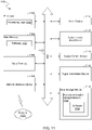
FIG. 11 illustrates a diagrammatic representation of a machine in the exemplary form of acomputer system 1100 within which a set of instructions, for causing the machine to perform any one or more of the methodologies described herein, may be executed. In alternative embodiments, the machine may be connected (e.g., networked) to other machines in a Local Area Network (LAN), an intranet, an extranet, or the Internet. The machine may operate in the capacity of a server or a client machine in a client-server network environment, or as a peer machine in a peer-to-peer (or distributed) network environment. The machine may be a personal computer (PC), a tablet PC, a set-top box (STB), a Personal Digital Assistant (PDA), a cellular telephone, a web appliance, a server, a network router, switch or bridge, or any machine capable of executing a set of instructions (sequential or otherwise) that specify actions to be taken by that machine. Further, while only a single machine is illustrated, the term "machine" shall also be taken to include any collection of machines (e.g., computers) that individually or jointly execute a set (or multiple sets) of instructions to perform any one or more of the methodologies described herein. - The
exemplary computer system 1100 includes aprocessor 1102, a main memory 1104 (e.g., read-only memory (ROM), flash memory, dynamic random access memory (DRAM) such as synchronous DRAM (SDRAM) or Rambus DRAM (RDRAM), etc.), a static memory 1106 (e.g., flash memory, static random access memory (SRAM), etc.), and a secondary memory 1118 (e.g., a data storage device), which communicate with each other via abus 1130. -
Processor 1102 represents one or more general-purpose processing devices such as a microprocessor, central processing unit, or the like. More particularly, theprocessor 1102 may be a complex instruction set computing (CISC) microprocessor, reduced instruction set computing (RISC) microprocessor, very long instruction word (VLIW) microprocessor, processor implementing other instruction sets, or processors implementing a combination of instruction sets.Processor 1102 may also be one or more special-purpose processing devices such as an application specific integrated circuit (ASIC), a field programmable gate array (FPGA), a digital signal processor (DSP), network processor, or the like.Processor 1102 is configured to execute theprocessing logic 1126 for performing the operations described herein. - The
computer system 1100 may further include anetwork interface device 1108. Thecomputer system 1100 also may include a video display unit 1110 (e.g., a liquid crystal display (LCD), a light emitting diode display (LED), or a cathode ray tube (CRT)), an alphanumeric input device 1112 (e.g., a keyboard), a cursor control device 1114 (e.g., a mouse), and a signal generation device 1116 (e.g., a speaker). - The
secondary memory 1118 may include a machine-accessible storage medium (or more specifically a computer-readable storage medium) 1132 on which is stored one or more sets of instructions (e.g., software 1122) embodying any one or more of the methodologies or functions described herein. Thesoftware 1122 may also reside, completely or at least partially, within themain memory 1104 and/or within theprocessor 1102 during execution thereof by thecomputer system 1100, themain memory 1104 and theprocessor 1102 also constituting machine-readable storage media. Thesoftware 1122 may further be transmitted or received over anetwork 1120 via thenetwork interface device 1108. - While the machine-
accessible storage medium 1132 is shown in an exemplary embodiment to be a single medium, the term "machine-readable storage medium" should be taken to include a single medium or multiple media (e.g., a centralized or distributed database, and/or associated caches and servers) that store the one or more sets of instructions. The term "machine-readable storage medium" shall also be taken to include any medium that is capable of storing or encoding a set of instructions for execution by the machine and that cause the machine to perform any of one or more embodiments. The term "machine-readable storage medium" shall accordingly be taken to include, but not be limited to, solid-state memories, and optical and magnetic media. -
FIG. 12 illustrates aninterposer 1200 that includes one or more embodiments. Theinterposer 1200 is an intervening substrate used to bridge afirst substrate 1202 to asecond substrate 1204. Thefirst substrate 1202 may be, for instance, an integrated circuit die. Thesecond substrate 1204 may be, for instance, a memory module, a computer motherboard, or another integrated circuit die. Generally, the purpose of aninterposer 1200 is to spread a connection to a wider pitch or to reroute a connection to a different connection. For example, aninterposer 1200 may couple an integrated circuit die to a ball grid array (BGA) 1206 that can subsequently be coupled to thesecond substrate 1204. In some embodiments, the first andsecond substrates interposer 1200. In other embodiments, the first andsecond substrates interposer 1200. And in further embodiments, three or more substrates are interconnected by way of theinterposer 1200. - The
interposer 1200 may be formed of an epoxy resin, a fiberglass-reinforced epoxy resin, a ceramic material, or a polymer material such as polyimide. In further implementations, the interposer may be formed of alternate rigid or flexible materials that may include the same materials described above for use in a semiconductor substrate, such as silicon, germanium, and other group III-V and group IV materials. - The interposer may include
metal interconnects 1208 and vias 1210, including but not limited to through-silicon vias (TSVs) 1212. Theinterposer 1200 may further include embeddeddevices 1214, including both passive and active devices. Such devices include, but are not limited to, capacitors, decoupling capacitors, resistors, inductors, fuses, diodes, transformers, sensors, and electrostatic discharge (ESD) devices. More complex devices such as radiofrequency (RF) devices, power amplifiers, power management devices, antennas, arrays, sensors, and MEMS devices may also be formed on theinterposer 1200. In accordance with some embodiments, apparatuses or processes disclosed herein may be used in the fabrication ofinterposer 1200. - In one or more first embodiments, a photonic device comprises a package substrate, and a photonic integrated circuit (PIC) chip which extends over a first region of the package substrate, the PIC chip comprising a plurality of coplanar photonic waveguides, and a plurality of coplanar integrated edge-oriented couplers (IECs), wherein individual ones of the plurality of coplanar IECs each terminate a respective one of the coplanar photonic waveguides with a respective divergent lens surface that is substantially flat over at least the thickness, wherein a planar optical waveguide structure of the photonic device extends over a second region of the package substrate, the planar optical waveguide structure comprising a core, wherein an edge of the core is adjacent to the plurality of coplanar IECs.
- In one or more second embodiments, further to the first embodiment, the planar optical waveguide structure is a waveguide preform which is coupled to the package substrate independent of the PIC.
- In one or more third embodiments, further to the first embodiment or the second embodiment, PIC comprises the planar optical waveguide structure.
- In one or more fourth embodiments, further to the first embodiment through third embodiments, the PIC forms a stepped structure, an upper portion of the stepped structure comprises the plurality of coplanar IECs, a lower portion of the stepped structure extends past the plurality of coplanar IECs, and the planar optical waveguide structure overlaps the lower portion.
- In one or more fifth embodiments, further to any of the first through fourth embodiments, the edge of the planar optical waveguide structure comprises a plurality of surface recesses, and individual ones of the plurality of surface recesses each interface with a corresponding one of the plurality of coplanar IECs.
- In one or more sixth embodiments, further to the fifth embodiment, individual ones of the plurality of surface recesses have a profile complementary to a profile of a respective divergent lens surface of the plurality of coplanar IECs.
- In one or more seventh embodiments, further to the sixth embodiment, individual ones of the plurality of surface recesses each form a respective substantially flat surface over at least a partial thickness of the core.
- In one or more eighth embodiments, further to the seventh embodiment, individual ones of the plurality of surface recesses extend through an entire thickness of a bottom cladding of the planar optical waveguide structure.
- In one or more ninth embodiments, further to the seventh embodiment, a first divergent lens surface of the plurality of coplanar IECs is semicylindrical, and a first surface recess of the plurality of surface recesses is semicylindrical.
- In one or more tenth embodiments, further to the fifth embodiment, the edge of the planar optical waveguide structure is a first edge, and the plurality of surface recesses is a first plurality of surface recesses, wherein a second edge of the planar optical waveguide structure, opposite the first edge, comprises a second plurality of concave lens surfaces.
- In one or more eleventh embodiments, further to the tenth embodiment, the second plurality of concave lens surfaces comprise a plurality of semispherical surfaces, and wherein the planar optical waveguide structure optically couples individual ones of the plurality of coplanar IECs to individual ones of the spherical surfaces.
- In one or more twelfth embodiments, further to the tenth embodiment, the photonic device further comprises a plurality of optical fibers over a third region of the package substrate, wherein individual ones of the optical fibers are optically coupled to individual ones of the second plurality of concave lens surfaces.
- In one or more thirteenth embodiments, further to any of the first through fifth embodiments, the edge of the planar optical waveguide structure is a first edge, the photonic device further comprises a plurality of optical fibers adjacent to a second edge of the planar optical waveguide structure, opposite the first edge.
- In one or more fourteenth embodiments, a photonic integrated circuit (PIC) chip comprises a substrate, a plurality of coplanar photonic waveguides within a thickness of a material over a plane of the substrate, and a plurality of coplanar integrated edge-oriented couplers (IECs), wherein individual ones of the plurality of coplanar IECs each terminate a respective one of the coplanar photonic waveguides with a respective divergent lens surface that is substantially flat over at least the thickness, wherein the PIC forms a stepped structure, an upper portion of the stepped structure comprises the plurality of coplanar IECs, and a lower portion of the stepped structure extends past the plurality of coplanar IECs.
- In one or more fifteenth embodiments, further to the fourteenth embodiment, the PIC chip further comprises a planar optical waveguide structure comprising a core, wherein an edge of the core is adjacent to the plurality of coplanar IECs.
- In one or more sixteenth embodiments, further to the fourteenth embodiment or the fifteenth embodiment, a first divergent lens surface of the plurality of coplanar IECs comprises a plurality of discrete diffractive edge facets symmetrically distributed about a primary axis of the first divergent lens surface, and wherein individual ones of the edge facets are substantially flat.
- In one or more seventeenth embodiments, further to any of the fourteenth through sixteenth embodiments, a first divergent lens surface of the plurality of coplanar IECs is substantially semicylindrical, and wherein a radius of curvature of the first divergent lens surface is symmetrical about a primary axis of the first divergent lens surface.
- In one or more eighteenth embodiments, further to the seventeenth embodiment, the primary axis of the first divergent lens surface is in a lateral alignment with an optical axis of a first photonic waveguide of the plurality of photonic waveguides, wherein the radius of curvature is equal to or larger than one half of a width of the first photonic waveguide.
- In one or more nineteenth embodiments, further to any of the fourteenth through seventeenth embodiments, a first divergent lens surface of the plurality of coplanar IECs extends a depth into the substrate.
- In one or more twentieth embodiments, further to the nineteenth embodiment, the material is silicon, and the substrate comprises an underlayer and a layer of silicon dioxide between the silicon and the underlayer.
- In one or more twenty-first embodiments, further to the twentieth embodiment, the first divergent lens surface stops at, or within, the layer of silicon dioxide.
- In one or more twenty-second embodiments, further to the twentieth embodiment, the first divergent lens surface extends at least partially through the underlayer.
- In one or more twenty-third embodiments, a system comprises a packaged device comprising package substrate, a photonic integrated circuit (PIC) chip which extends over a first region of the package substrate, the PIC chip comprising a plurality of coplanar photonic waveguides within a thickness of a material over a plane of the substrate, a plurality of coplanar integrated edge-oriented couplers (IECs), wherein individual ones of the plurality of coplanar IECs each terminate a respective one of the coplanar photonic waveguides with a respective divergent lens surface that is substantially flat over at least the thickness wherein a planar optical waveguide structure of the photonic device is over a second region of the package substrate, planar optical waveguide structure comprising a core, wherein an edge of the core is adjacent to the plurality of coplanar IECs, a connector coupled to the packaged device, the connector comprising an array of optical fibers adjacent to the planar optical waveguide structure, and a printed circuit board coupled to the packaged circuit device.
- In one or more twenty-fourth embodiments, further to the twenty-third embodiment, the planar optical waveguide structure is a waveguide preform which is coupled to the package substrate independent of the PIC.
- In one or more twenty-fifth embodiments, further to the twenty-third embodiment or the twenty-fourth embodiment, the PIC comprises the planar optical waveguide structure.
- In one or more twenty-sixth embodiments, further to any of the twenty-third through twenty-fifth embodiments, an edge of the PIC forms a stepped structure, an upper portion of the stepped structure comprises the plurality of coplanar IECs, a lower portion of the stepped structure extends past the plurality of coplanar IECs, and the planar optical waveguide structure overlaps the lower portion.
- In one or more twenty-seventh embodiments, further to any of the twenty-third through twenty-sixth embodiments, the edge of the planar optical waveguide structure comprises a plurality of surface recesses, and individual ones of the plurality of surface recesses each interface with a corresponding one of the plurality of coplanar IECs.
- In one or more twenty-eighth embodiments, further to the twenty-seventh embodiment, individual ones of the plurality of surface recesses have a profile complementary to a profile of a respective divergent lens surface of the plurality of coplanar IECs.
- In one or more twenty-ninth embodiments, further to the twenty-eighth embodiment, individual ones of the plurality of surface recesses each form a respective substantially flat surface over at least a partial thickness of the core.
- In one or more thirtieth embodiments, further to the twenty-ninth embodiment, individual ones of the plurality of surface recesses extend through an entire thickness of a bottom cladding of the planar optical waveguide structure.
- In one or more thirty-first embodiments, further to the twenty-ninth embodiment, a first divergent lens surface of the plurality of coplanar IECs is semicylindrical, and a first surface recess of the plurality of surface recesses is semicylindrical.
- In one or more thirty-second embodiments, further to the twenty-seventh embodiment, the edge of the planar optical waveguide structure is a first edge, and the plurality of surface recesses is a first plurality of surface recesses, wherein a second edge of the planar optical waveguide structure, opposite the first edge, comprises a second plurality of concave lens surfaces.
- In one or more thirty-third embodiments, further to the thirty-third embodiment, the second plurality of concave lens surfaces comprise a plurality of semispherical surfaces, and wherein the planar optical waveguide structure optically couples individual ones of the plurality of coplanar IECs to individual ones of the spherical surfaces.
- In one or more thirty-fourth embodiments, a method comprises receiving a substrate, patterning a plurality of coplanar optical waveguides into a thickness of a material over a plane of the substrate, subtractively patterning divergent lens profiles each at a terminus of a respective one of the plurality of coplanar optical waveguides, wherein the divergent lens profiles are each substantially flat over at least the thickness, and singulating a photonic integrated circuit (PIC) chip comprising the plurality of coplanar optical waveguides, the divergent lens profiles, and a portion of the substate, wherein integrated edge-oriented couplers (IECs) of the PIC chip each comprise a respective one of the divergent lens profiles.
- In one or more thirty-fifth embodiments, further to the thirty-fourth embodiment, the material is silicon, and wherein the substrate comprises an underlayer and a layer of silicon dioxide between the silicon and the underlayer, the method further comprising removing a portion of the silicon to expose a region of the layer of silicon dioxide, and forming a planar optical waveguide structure on the region, the planar optical waveguide structure comprising a core, wherein an edge of the core is adjacent to the plurality of coplanar IECs.
- In one or more thirty-sixth embodiments, further to the thirty-fourth embodiment or the thirty-fifth embodiment, subtractively patterning the divergent lens profiles comprises masking the material and anisotropically etching through the thickness of the material.
- In one or more thirty-seventh embodiments, further to the thirty-sixth embodiment, the etching is stopped within the substrate.
- In one or more thirty-eighth embodiments, further to any of the thirty-fourth through thirty-fifth embodiments, the method further comprises coupling the PIC chip over a first region of a package substrate, coupling a planar optical waveguide structure over a second region of the package substrate, the planar optical waveguide structure comprising a core, wherein an edge of the core is adjacent to the plurality of coplanar IECs
- In one or more thirty-ninth embodiments, further to the thirty-eighth embodiment, the method further comprises coupling an array of optical fibers to the planar optical waveguide structure.
- Techniques and architectures for optically coupling a photonic integrated circuit with optical fibers via a waveguide are described herein. In the above description, for purposes of explanation, numerous specific details are set forth in order to provide a thorough understanding of certain embodiments. It will be apparent, however, to one skilled in the art that certain embodiments can be practiced without these specific details. In other instances, structures and devices are shown in block diagram form in order to avoid obscuring the description.
- Reference in the specification to "one embodiment" or "an embodiment" means that a particular feature, structure, or characteristic described in connection with the embodiment is included in at least one embodiment of the invention. The appearances of the phrase "in one embodiment" in various places in the specification are not necessarily all referring to the same embodiment.
- Some portions of the detailed description herein are presented in terms of algorithms and symbolic representations of operations on data bits within a computer memory. These algorithmic descriptions and representations are the means used by those skilled in the computing arts to most effectively convey the substance of their work to others skilled in the art. An algorithm is here, and generally, conceived to be a self-consistent sequence of steps leading to a desired result. The steps are those requiring physical manipulations of physical quantities. Usually, though not necessarily, these quantities take the form of electrical or magnetic signals capable of being stored, transferred, combined, compared, and otherwise manipulated. It has proven convenient at times, principally for reasons of common usage, to refer to these signals as bits, values, elements, symbols, characters, terms, numbers, or the like.
- It should be borne in mind, however, that all of these and similar terms are to be associated with the appropriate physical quantities and are merely convenient labels applied to these quantities. Unless specifically stated otherwise as apparent from the discussion herein, it is appreciated that throughout the description, discussions utilizing terms such as "processing" or "computing" or "calculating" or "determining" or "displaying" or the like, refer to the action and processes of a computer system, or similar electronic computing device, that manipulates and transforms data represented as physical (electronic) quantities within the computer system's registers and memories into other data similarly represented as physical quantities within the computer system memories or registers or other such information storage, transmission or display devices.
- Certain embodiments also relate to apparatus for performing the operations herein. This apparatus may be specially constructed for the required purposes, or it may comprise a general purpose computer selectively activated or reconfigured by a computer program stored in the computer. Such a computer program may be stored in a computer readable storage medium, such as, but is not limited to, any type of disk including floppy disks, optical disks, CD-ROMs, and magnetic-optical disks, read-only memories (ROMs), random access memories (RAMs) such as dynamic RAM (DRAM), EPROMs, EEPROMs, magnetic or optical cards, or any type of media suitable for storing electronic instructions, and coupled to a computer system bus.
- The algorithms and displays presented herein are not inherently related to any particular computer or other apparatus. Various general purpose systems may be used with programs in accordance with the teachings herein, or it may prove convenient to construct more specialized apparatus to perform the required method steps. The required structure for a variety of these systems will appear from the description herein. In addition, certain embodiments are not described with reference to any particular programming language. It will be appreciated that a variety of programming languages may be used to implement the teachings of such embodiments as described herein.
- Besides what is described herein, various modifications may be made to the disclosed embodiments and implementations thereof without departing from their scope. Therefore, the illustrations and examples herein should be construed in an illustrative, and not a restrictive sense. The scope of the invention should be measured solely by reference to the claims that follow.
Claims (15)
- A photonic device comprising:a package substrate; anda photonic integrated circuit (PIC) chip which extends over a first region of the package substrate, the PIC chip comprising:a plurality of coplanar photonic waveguides; anda plurality of coplanar integrated edge-oriented couplers (IECs), wherein individual ones of the plurality of coplanar IECs each terminate a respective one of the coplanar photonic waveguides with a respective divergent lens surface that issubstantially flat over at least the thickness;wherein a planar optical waveguide structure of the photonic device extends over a second region of the package substrate, the planar optical waveguide structure comprising a core, wherein an edge of the core is adjacent to the plurality of coplanar IECs.
- The photonic device of claim 1, wherein the planar optical waveguide structure is a waveguide preform which is coupled to the package substrate independent of the PIC.
- The photonic device of claim 1, wherein PIC comprises the planar optical waveguide structure.
- The photonic device of any of claim 1 through claim 3, wherein:the PIC forms a stepped structure;an upper portion of the stepped structure comprises the plurality of coplanar IECs;a lower portion of the stepped structure extends past the plurality of coplanar IECs; andthe planar optical waveguide structure overlaps the lower portion.
- The photonic device of any of claim 1 through claim 3, wherein:the edge of the planar optical waveguide structure comprises a plurality of surface recesses; andindividual ones of the plurality of surface recesses each interface with a corresponding one of the plurality of coplanar IECs.
- The photonic device of claim 5, wherein individual ones of the plurality of surface recesses have a profile complementary to a profile of a respective divergent lens surface of the plurality of coplanar IECs.
- The photonic device of claim 6, wherein individual ones of the plurality of surface recesses each form a respective substantially flat surface over at least a partial thickness of the core.
- The photonic device of claim 7, wherein individual ones of the plurality of surface recesses extend through an entire thickness of a bottom cladding of the planar optical waveguide structure.
- The photonic device of claim 5, wherein the edge of the planar optical waveguide structure is a first edge, and the plurality of surface recesses is a first plurality of surface recesses, wherein a second edge of the planar optical waveguide structure, opposite the first edge, comprises a second plurality of concave lens surfaces.
- The photonic device of any of claim 1 through claim 3, wherein the edge of the planar optical waveguide structure is a first edge, the photonic device further comprising a plurality of optical fibers adjacent to a second edge of the planar optical waveguide structure, opposite the first edge.
- A method comprising:receiving a substrate;patterning a plurality of coplanar optical waveguides into a thickness of a material over a plane of the substrate;subtractively patterning divergent lens profiles each at a terminus of a respective one of the plurality of coplanar optical waveguides, wherein the divergent lens profiles are each substantially flat over at least the thickness; andsingulating a photonic integrated circuit (PIC) chip comprising the plurality of coplanar optical waveguides, the divergent lens profiles, and a portion of the substate, wherein integrated edge-oriented couplers (IECs) of the PIC chip each comprise a respective one of the divergent lens profiles.
- The method of claim 11, wherein the material is silicon, and wherein the substrate comprises an underlayer and a layer of silicon dioxide between the silicon and the underlayer, the method further comprising:removing a portion of the silicon to expose a region of the layer of silicon dioxide; andforming a planar optical waveguide structure on the region, the planar optical waveguide structure comprising a core, wherein an edge of the core is adjacent to the plurality of coplanar IECs.
- The method of either of claim 11 or claim 12, wherein subtractively patterning the divergent lens profiles comprises masking the material and anisotropically etching through the thickness of the material.
- The method of claim 13, wherein the etching is stopped within the substrate.
- The method of either of claim 11 or claim 12, further comprising:coupling the PIC chip over a first region of a package substrate;coupling a planar optical waveguide structure over a second region of the package substrate, the planar optical waveguide structure comprising a core, wherein an edge of the core is adjacent to the plurality of coplanar IECs
Applications Claiming Priority (1)
| Application Number | Priority Date | Filing Date | Title |
|---|---|---|---|
| US17/359,178 US12164147B2 (en) | 2021-06-25 | 2021-06-25 | Device, method and system for optical communication with a waveguide structure and an integrated optical coupler of a photonic integrated circuit chip |
Publications (2)
| Publication Number | Publication Date |
|---|---|
| EP4109151A1 true EP4109151A1 (en) | 2022-12-28 |
| EP4109151B1 EP4109151B1 (en) | 2024-09-04 |
Family
ID=80781003
Family Applications (1)
| Application Number | Title | Priority Date | Filing Date |
|---|---|---|---|
| EP22162068.5A Active EP4109151B1 (en) | 2021-06-25 | 2022-03-15 | Device, method and system for optical communication with a waveguide structure and an integrated optical coupler of a photonic integrated circuit chip |
Country Status (3)
| Country | Link |
|---|---|
| US (1) | US12164147B2 (en) |
| EP (1) | EP4109151B1 (en) |
| CN (1) | CN115524794A (en) |
Families Citing this family (9)
| Publication number | Priority date | Publication date | Assignee | Title |
|---|---|---|---|---|
| US12164147B2 (en) * | 2021-06-25 | 2024-12-10 | Intel Corporation | Device, method and system for optical communication with a waveguide structure and an integrated optical coupler of a photonic integrated circuit chip |
| US12298572B2 (en) * | 2021-06-25 | 2025-05-13 | Intel Corporation | Device, method and system for optical communication with a photonic integrated circuit chip and a transverse oriented lens structure |
| US11835757B2 (en) * | 2021-10-01 | 2023-12-05 | Advanced Semiconductor Engineering, Inc. | Optoelectronic package and method for manufacturing the same |
| US12332478B2 (en) * | 2022-03-18 | 2025-06-17 | Taiwan Semiconductor Manufacturing Company, Ltd. | Photonic device and methods of forming same |
| US12386119B2 (en) * | 2022-03-30 | 2025-08-12 | Taiwan Semiconductor Manufacturing Company, Ltd. | Facet profile to improve edge coupler beam pointing and coupling efficiency for photonics |
| US12487417B2 (en) * | 2022-10-04 | 2025-12-02 | Applied Materials, Inc. | Photonic glass layer substrate with embedded optical structures for communicating with an electro optical integrated circuit |
| US20240194657A1 (en) * | 2022-12-13 | 2024-06-13 | Intel Corporation | Integrated photonic device and electronic device architectures |
| CN116679388B (en) * | 2023-06-12 | 2025-02-07 | Nano科技(北京)有限公司 | A fiber array structure coupled with a silicon photonic integrated chip |
| US12613376B2 (en) | 2023-06-29 | 2026-04-28 | Intel Corporation | Optical isolators for multi-channel optical interconnects |
Citations (6)
| Publication number | Priority date | Publication date | Assignee | Title |
|---|---|---|---|---|
| US4755014A (en) * | 1986-06-20 | 1988-07-05 | Northrop Corporation | Refractive optical waveguide interface and lens |
| US4756591A (en) * | 1984-02-09 | 1988-07-12 | Siemens Aktiengesellschaft | Device for releasable coupling of an optical fiber to an optoelectronic component |
| DE19613755A1 (en) * | 1996-04-06 | 1997-10-09 | Sel Alcatel Ag | Optical coupler for light guide structures |
| US6810190B2 (en) * | 2001-08-07 | 2004-10-26 | Massachusetts Institute Of Technology | Compact three-dimensional mode size converters for fiber-waveguide coupling |
| US20160139338A1 (en) * | 2013-04-12 | 2016-05-19 | Hon Hai Precision Industry Co., Ltd. | Optical connector having waveguide and method for manufacturing same |
| US9698564B1 (en) * | 2016-02-09 | 2017-07-04 | Oracle International Corporation | Hybrid integrated MCM with waveguide-fiber connector |
Family Cites Families (23)
| Publication number | Priority date | Publication date | Assignee | Title |
|---|---|---|---|---|
| JPH0744313B2 (en) * | 1989-02-24 | 1995-05-15 | 日本電信電話株式会社 | Semiconductor laser device |
| US5977567A (en) | 1998-01-06 | 1999-11-02 | Lightlogic, Inc. | Optoelectronic assembly and method of making the same |
| JP4665240B2 (en) | 2001-06-25 | 2011-04-06 | 富士通株式会社 | Optical transmission equipment |
| EP1376179A3 (en) * | 2002-06-27 | 2004-04-14 | Toyoda Koki Kabushiki Kaisha | Laminated optical waveguide array, optical beam collecting device and laser emission device |
| US20040120672A1 (en) | 2002-12-18 | 2004-06-24 | Gabel Chong | Waveguides with integrated lenses and reflective surfaces |
| JP4161745B2 (en) * | 2003-03-06 | 2008-10-08 | 株式会社デンソー | Optical element and manufacturing method thereof |
| US20050048409A1 (en) | 2003-08-29 | 2005-03-03 | Elqaq Deirdre H. | Method of making an optical device in silicon |
| US20050105853A1 (en) | 2003-11-13 | 2005-05-19 | Ansheng Liu | Method and apparatus for dual tapering an optical waveguide |
| US7676131B2 (en) * | 2004-06-04 | 2010-03-09 | Poa Sana Liquidating Trust | Waveguide with a three-dimensional lens |
| KR20070103478A (en) * | 2005-02-07 | 2007-10-23 | 알피오 피티와이 리미티드 | Waveguide structure incorporating reflective optics |
| JP4847389B2 (en) | 2007-04-11 | 2011-12-28 | 日東電工株式会社 | Optical waveguide for touch panel and touch panel using the same |
| JP5007280B2 (en) | 2008-07-10 | 2012-08-22 | 日東電工株式会社 | Method for producing optical waveguide for touch panel and optical waveguide for touch panel obtained thereby |
| US7643710B1 (en) | 2008-09-17 | 2010-01-05 | Intel Corporation | Method and apparatus for efficient coupling between silicon photonic chip and optical fiber |
| US8319237B2 (en) | 2009-12-31 | 2012-11-27 | Intel Corporation | Integrated optical receiver architecture for high speed optical I/O applications |
| US9229169B2 (en) | 2011-08-16 | 2016-01-05 | International Business Machines Corporation | Lens array optical coupling to photonic chip |
| WO2013089755A1 (en) | 2011-12-15 | 2013-06-20 | Intel Corporation | An efficient backside-emitting/collecting grating coupler |
| US9664858B2 (en) | 2012-12-20 | 2017-05-30 | Intel Corporation | Optical photonic circuit coupling |
| WO2015191659A1 (en) | 2014-06-13 | 2015-12-17 | TeraDiode, Inc. | Optical alignment systems and methods for wavelength beam combining laser systems |
| US9971089B2 (en) | 2015-12-09 | 2018-05-15 | Intel Corporation | Chip-to-chip interconnect with embedded electro-optical bridge structures |
| US10242976B2 (en) | 2016-12-31 | 2019-03-26 | Intel Corporation | In-package photonics integration and assembly architecture |
| US10996408B2 (en) | 2019-07-19 | 2021-05-04 | Intel Corporation | Optical device including buried optical waveguides and output couplers |
| US12298572B2 (en) * | 2021-06-25 | 2025-05-13 | Intel Corporation | Device, method and system for optical communication with a photonic integrated circuit chip and a transverse oriented lens structure |
| US12164147B2 (en) * | 2021-06-25 | 2024-12-10 | Intel Corporation | Device, method and system for optical communication with a waveguide structure and an integrated optical coupler of a photonic integrated circuit chip |
-
2021
- 2021-06-25 US US17/359,178 patent/US12164147B2/en active Active
-
2022
- 2022-03-15 EP EP22162068.5A patent/EP4109151B1/en active Active
- 2022-05-24 CN CN202210570901.9A patent/CN115524794A/en active Pending
Patent Citations (6)
| Publication number | Priority date | Publication date | Assignee | Title |
|---|---|---|---|---|
| US4756591A (en) * | 1984-02-09 | 1988-07-12 | Siemens Aktiengesellschaft | Device for releasable coupling of an optical fiber to an optoelectronic component |
| US4755014A (en) * | 1986-06-20 | 1988-07-05 | Northrop Corporation | Refractive optical waveguide interface and lens |
| DE19613755A1 (en) * | 1996-04-06 | 1997-10-09 | Sel Alcatel Ag | Optical coupler for light guide structures |
| US6810190B2 (en) * | 2001-08-07 | 2004-10-26 | Massachusetts Institute Of Technology | Compact three-dimensional mode size converters for fiber-waveguide coupling |
| US20160139338A1 (en) * | 2013-04-12 | 2016-05-19 | Hon Hai Precision Industry Co., Ltd. | Optical connector having waveguide and method for manufacturing same |
| US9698564B1 (en) * | 2016-02-09 | 2017-07-04 | Oracle International Corporation | Hybrid integrated MCM with waveguide-fiber connector |
Non-Patent Citations (1)
| Title |
|---|
| MINOT M M ET AL: "A NEW GUIDED-WAVE LENS STRUCTURE", JOURNAL OF LIGHTWAVE TECHNOLOGY, IEEE, USA, vol. 8, no. 12, 1 December 1990 (1990-12-01), pages 1856 - 1865, XP000204665, ISSN: 0733-8724, DOI: 10.1109/50.62883 * |
Also Published As
| Publication number | Publication date |
|---|---|
| US20220413210A1 (en) | 2022-12-29 |
| EP4109151B1 (en) | 2024-09-04 |
| CN115524794A (en) | 2022-12-27 |
| US12164147B2 (en) | 2024-12-10 |
Similar Documents
| Publication | Publication Date | Title |
|---|---|---|
| EP4109151A1 (en) | Device, method and system for optical communication with a waveguide structure and an integrated optical coupler of a photonic integrated circuit chip | |
| US10598875B2 (en) | Photonic package with a bridge between a photonic die and an optical coupling structure | |
| US20260099015A1 (en) | Photonic integrated circuit packaging architectures | |
| US20230204879A1 (en) | Optical packaging using embedded-in-mold (eim) optical module integration | |
| US11251228B2 (en) | Optical receiver package with backside lens-integrated photodetector die | |
| US12392970B2 (en) | Photonic integrated circuit packaging architectures | |
| US12298572B2 (en) | Device, method and system for optical communication with a photonic integrated circuit chip and a transverse oriented lens structure | |
| US12399334B2 (en) | Photonic integrated circuit packaging architectures | |
| EP4310563A1 (en) | Improved photonics integrated circuit device packaging | |
| US20230089877A1 (en) | Photonic integrated circuit packaging architectures | |
| US20230087809A1 (en) | Photonic integrated circuit packaging architectures | |
| US20230089494A1 (en) | Photonic integrated circuit packaging architectures | |
| US20240027710A1 (en) | Embedded photonics integrated circuit in glass core of substrate | |
| US20240176068A1 (en) | Photonic integrated circuit packages including substrates with glass cores | |
| US20240027699A1 (en) | Technologies for a beam expansion in glass substrates | |
| US20240027697A1 (en) | Pluggable optical connector with interfacial alignment features | |
| US12591096B2 (en) | Technologies for a beam expansion and collimation for photonic integrated circuits | |
| CN119065073A (en) | Optical connector for kinematic alignment of silicon photonic integrated circuits (PICs) and method of manufacturing the same | |
| US20250110270A1 (en) | Optical co-packaging on a glass substrate with 3d die-stacking | |
| US20240395567A1 (en) | Selective underfilling using pre-applied thermoset adhesive | |
| US20250110289A1 (en) | Optical connector ferrule | |
| US20240176069A1 (en) | Photonic integrated circuit packages including substrates with glass cores | |
| CN118091832A (en) | Photonic integrated circuit package including a substrate having a glass core | |
| US20260086307A1 (en) | Optical coupling using shifted out-of-plane light propagation | |
| US20250004219A1 (en) | Architecture and method for passive-active optical alignment of photonic integrated circuit (pic) and fiber array unit (fau) |
Legal Events
| Date | Code | Title | Description |
|---|---|---|---|
| PUAI | Public reference made under article 153(3) epc to a published international application that has entered the european phase |
Free format text: ORIGINAL CODE: 0009012 |
|
| STAA | Information on the status of an ep patent application or granted ep patent |
Free format text: STATUS: THE APPLICATION HAS BEEN PUBLISHED |
|
| AK | Designated contracting states |
Kind code of ref document: A1 Designated state(s): AL AT BE BG CH CY CZ DE DK EE ES FI FR GB GR HR HU IE IS IT LI LT LU LV MC MK MT NL NO PL PT RO RS SE SI SK SM TR |
|
| STAA | Information on the status of an ep patent application or granted ep patent |
Free format text: STATUS: REQUEST FOR EXAMINATION WAS MADE |
|
| 17P | Request for examination filed |
Effective date: 20230628 |
|
| RBV | Designated contracting states (corrected) |
Designated state(s): AL AT BE BG CH CY CZ DE DK EE ES FI FR GB GR HR HU IE IS IT LI LT LU LV MC MK MT NL NO PL PT RO RS SE SI SK SM TR |
|
| GRAP | Despatch of communication of intention to grant a patent |
Free format text: ORIGINAL CODE: EPIDOSNIGR1 |
|
| STAA | Information on the status of an ep patent application or granted ep patent |
Free format text: STATUS: GRANT OF PATENT IS INTENDED |
|
| INTG | Intention to grant announced |
Effective date: 20240404 |
|
| GRAS | Grant fee paid |
Free format text: ORIGINAL CODE: EPIDOSNIGR3 |
|
| GRAA | (expected) grant |
Free format text: ORIGINAL CODE: 0009210 |
|
| STAA | Information on the status of an ep patent application or granted ep patent |
Free format text: STATUS: THE PATENT HAS BEEN GRANTED |
|
| AK | Designated contracting states |
Kind code of ref document: B1 Designated state(s): AL AT BE BG CH CY CZ DE DK EE ES FI FR GB GR HR HU IE IS IT LI LT LU LV MC MK MT NL NO PL PT RO RS SE SI SK SM TR |
|
| REG | Reference to a national code |
Ref country code: GB Ref legal event code: FG4D |
|
| REG | Reference to a national code |
Ref country code: CH Ref legal event code: EP |
|
| P01 | Opt-out of the competence of the unified patent court (upc) registered |
Free format text: CASE NUMBER: APP_47523/2024 Effective date: 20240817 |
|
| REG | Reference to a national code |
Ref country code: IE Ref legal event code: FG4D |
|
| REG | Reference to a national code |
Ref country code: DE Ref legal event code: R096 Ref document number: 602022005772 Country of ref document: DE |
|
| REG | Reference to a national code |
Ref country code: NL Ref legal event code: FP |
|
| REG | Reference to a national code |
Ref country code: LT Ref legal event code: MG9D |
|
| PG25 | Lapsed in a contracting state [announced via postgrant information from national office to epo] |
Ref country code: NO Free format text: LAPSE BECAUSE OF FAILURE TO SUBMIT A TRANSLATION OF THE DESCRIPTION OR TO PAY THE FEE WITHIN THE PRESCRIBED TIME-LIMIT Effective date: 20241204 |
|
| PG25 | Lapsed in a contracting state [announced via postgrant information from national office to epo] |
Ref country code: GR Free format text: LAPSE BECAUSE OF FAILURE TO SUBMIT A TRANSLATION OF THE DESCRIPTION OR TO PAY THE FEE WITHIN THE PRESCRIBED TIME-LIMIT Effective date: 20241205 Ref country code: PL Free format text: LAPSE BECAUSE OF FAILURE TO SUBMIT A TRANSLATION OF THE DESCRIPTION OR TO PAY THE FEE WITHIN THE PRESCRIBED TIME-LIMIT Effective date: 20240904 Ref country code: FI Free format text: LAPSE BECAUSE OF FAILURE TO SUBMIT A TRANSLATION OF THE DESCRIPTION OR TO PAY THE FEE WITHIN THE PRESCRIBED TIME-LIMIT Effective date: 20240904 |
|
| PG25 | Lapsed in a contracting state [announced via postgrant information from national office to epo] |
Ref country code: BG Free format text: LAPSE BECAUSE OF FAILURE TO SUBMIT A TRANSLATION OF THE DESCRIPTION OR TO PAY THE FEE WITHIN THE PRESCRIBED TIME-LIMIT Effective date: 20240904 |
|
| PG25 | Lapsed in a contracting state [announced via postgrant information from national office to epo] |
Ref country code: LV Free format text: LAPSE BECAUSE OF FAILURE TO SUBMIT A TRANSLATION OF THE DESCRIPTION OR TO PAY THE FEE WITHIN THE PRESCRIBED TIME-LIMIT Effective date: 20240904 |
|
| PG25 | Lapsed in a contracting state [announced via postgrant information from national office to epo] |
Ref country code: HR Free format text: LAPSE BECAUSE OF FAILURE TO SUBMIT A TRANSLATION OF THE DESCRIPTION OR TO PAY THE FEE WITHIN THE PRESCRIBED TIME-LIMIT Effective date: 20240904 |
|
| PG25 | Lapsed in a contracting state [announced via postgrant information from national office to epo] |
Ref country code: RS Free format text: LAPSE BECAUSE OF FAILURE TO SUBMIT A TRANSLATION OF THE DESCRIPTION OR TO PAY THE FEE WITHIN THE PRESCRIBED TIME-LIMIT Effective date: 20241204 Ref country code: ES Free format text: LAPSE BECAUSE OF FAILURE TO SUBMIT A TRANSLATION OF THE DESCRIPTION OR TO PAY THE FEE WITHIN THE PRESCRIBED TIME-LIMIT Effective date: 20240904 |
|
| PG25 | Lapsed in a contracting state [announced via postgrant information from national office to epo] |
Ref country code: RS Free format text: LAPSE BECAUSE OF FAILURE TO SUBMIT A TRANSLATION OF THE DESCRIPTION OR TO PAY THE FEE WITHIN THE PRESCRIBED TIME-LIMIT Effective date: 20241204 Ref country code: PL Free format text: LAPSE BECAUSE OF FAILURE TO SUBMIT A TRANSLATION OF THE DESCRIPTION OR TO PAY THE FEE WITHIN THE PRESCRIBED TIME-LIMIT Effective date: 20240904 Ref country code: NO Free format text: LAPSE BECAUSE OF FAILURE TO SUBMIT A TRANSLATION OF THE DESCRIPTION OR TO PAY THE FEE WITHIN THE PRESCRIBED TIME-LIMIT Effective date: 20241204 Ref country code: LV Free format text: LAPSE BECAUSE OF FAILURE TO SUBMIT A TRANSLATION OF THE DESCRIPTION OR TO PAY THE FEE WITHIN THE PRESCRIBED TIME-LIMIT Effective date: 20240904 Ref country code: HR Free format text: LAPSE BECAUSE OF FAILURE TO SUBMIT A TRANSLATION OF THE DESCRIPTION OR TO PAY THE FEE WITHIN THE PRESCRIBED TIME-LIMIT Effective date: 20240904 Ref country code: GR Free format text: LAPSE BECAUSE OF FAILURE TO SUBMIT A TRANSLATION OF THE DESCRIPTION OR TO PAY THE FEE WITHIN THE PRESCRIBED TIME-LIMIT Effective date: 20241205 Ref country code: FI Free format text: LAPSE BECAUSE OF FAILURE TO SUBMIT A TRANSLATION OF THE DESCRIPTION OR TO PAY THE FEE WITHIN THE PRESCRIBED TIME-LIMIT Effective date: 20240904 Ref country code: ES Free format text: LAPSE BECAUSE OF FAILURE TO SUBMIT A TRANSLATION OF THE DESCRIPTION OR TO PAY THE FEE WITHIN THE PRESCRIBED TIME-LIMIT Effective date: 20240904 Ref country code: BG Free format text: LAPSE BECAUSE OF FAILURE TO SUBMIT A TRANSLATION OF THE DESCRIPTION OR TO PAY THE FEE WITHIN THE PRESCRIBED TIME-LIMIT Effective date: 20240904 |
|
| REG | Reference to a national code |
Ref country code: AT Ref legal event code: MK05 Ref document number: 1720963 Country of ref document: AT Kind code of ref document: T Effective date: 20240904 |
|
| PG25 | Lapsed in a contracting state [announced via postgrant information from national office to epo] |
Ref country code: IS Free format text: LAPSE BECAUSE OF FAILURE TO SUBMIT A TRANSLATION OF THE DESCRIPTION OR TO PAY THE FEE WITHIN THE PRESCRIBED TIME-LIMIT Effective date: 20250104 Ref country code: PT Free format text: LAPSE BECAUSE OF FAILURE TO SUBMIT A TRANSLATION OF THE DESCRIPTION OR TO PAY THE FEE WITHIN THE PRESCRIBED TIME-LIMIT Effective date: 20250106 |
|
| PG25 | Lapsed in a contracting state [announced via postgrant information from national office to epo] |
Ref country code: RO Free format text: LAPSE BECAUSE OF FAILURE TO SUBMIT A TRANSLATION OF THE DESCRIPTION OR TO PAY THE FEE WITHIN THE PRESCRIBED TIME-LIMIT Effective date: 20240904 Ref country code: SM Free format text: LAPSE BECAUSE OF FAILURE TO SUBMIT A TRANSLATION OF THE DESCRIPTION OR TO PAY THE FEE WITHIN THE PRESCRIBED TIME-LIMIT Effective date: 20240904 |
|
| PG25 | Lapsed in a contracting state [announced via postgrant information from national office to epo] |
Ref country code: EE Free format text: LAPSE BECAUSE OF FAILURE TO SUBMIT A TRANSLATION OF THE DESCRIPTION OR TO PAY THE FEE WITHIN THE PRESCRIBED TIME-LIMIT Effective date: 20240904 Ref country code: AT Free format text: LAPSE BECAUSE OF FAILURE TO SUBMIT A TRANSLATION OF THE DESCRIPTION OR TO PAY THE FEE WITHIN THE PRESCRIBED TIME-LIMIT Effective date: 20240904 |
|
| PG25 | Lapsed in a contracting state [announced via postgrant information from national office to epo] |
Ref country code: CZ Free format text: LAPSE BECAUSE OF FAILURE TO SUBMIT A TRANSLATION OF THE DESCRIPTION OR TO PAY THE FEE WITHIN THE PRESCRIBED TIME-LIMIT Effective date: 20240904 |
|
| PG25 | Lapsed in a contracting state [announced via postgrant information from national office to epo] |
Ref country code: IT Free format text: LAPSE BECAUSE OF FAILURE TO SUBMIT A TRANSLATION OF THE DESCRIPTION OR TO PAY THE FEE WITHIN THE PRESCRIBED TIME-LIMIT Effective date: 20240904 Ref country code: SK Free format text: LAPSE BECAUSE OF FAILURE TO SUBMIT A TRANSLATION OF THE DESCRIPTION OR TO PAY THE FEE WITHIN THE PRESCRIBED TIME-LIMIT Effective date: 20240904 |
|
| REG | Reference to a national code |
Ref country code: DE Ref legal event code: R097 Ref document number: 602022005772 Country of ref document: DE |
|
| PG25 | Lapsed in a contracting state [announced via postgrant information from national office to epo] |
Ref country code: DK Free format text: LAPSE BECAUSE OF FAILURE TO SUBMIT A TRANSLATION OF THE DESCRIPTION OR TO PAY THE FEE WITHIN THE PRESCRIBED TIME-LIMIT Effective date: 20240904 |
|
| PLBE | No opposition filed within time limit |
Free format text: ORIGINAL CODE: 0009261 |
|
| STAA | Information on the status of an ep patent application or granted ep patent |
Free format text: STATUS: NO OPPOSITION FILED WITHIN TIME LIMIT |
|
| 26N | No opposition filed |
Effective date: 20250605 |
|
| PG25 | Lapsed in a contracting state [announced via postgrant information from national office to epo] |
Ref country code: SE Free format text: LAPSE BECAUSE OF FAILURE TO SUBMIT A TRANSLATION OF THE DESCRIPTION OR TO PAY THE FEE WITHIN THE PRESCRIBED TIME-LIMIT Effective date: 20240904 |
|
| PG25 | Lapsed in a contracting state [announced via postgrant information from national office to epo] |
Ref country code: MC Free format text: LAPSE BECAUSE OF FAILURE TO SUBMIT A TRANSLATION OF THE DESCRIPTION OR TO PAY THE FEE WITHIN THE PRESCRIBED TIME-LIMIT Effective date: 20240904 |
|
| REG | Reference to a national code |
Ref country code: CH Ref legal event code: H13 Free format text: ST27 STATUS EVENT CODE: U-0-0-H10-H13 (AS PROVIDED BY THE NATIONAL OFFICE) Effective date: 20251023 |
|
| PG25 | Lapsed in a contracting state [announced via postgrant information from national office to epo] |
Ref country code: LU Free format text: LAPSE BECAUSE OF NON-PAYMENT OF DUE FEES Effective date: 20250315 |
|
| REG | Reference to a national code |
Ref country code: BE Ref legal event code: MM Effective date: 20250331 |
|
| PG25 | Lapsed in a contracting state [announced via postgrant information from national office to epo] |
Ref country code: BE Free format text: LAPSE BECAUSE OF NON-PAYMENT OF DUE FEES Effective date: 20250331 |
|
| PG25 | Lapsed in a contracting state [announced via postgrant information from national office to epo] |
Ref country code: CH Free format text: LAPSE BECAUSE OF NON-PAYMENT OF DUE FEES Effective date: 20250331 |
|
| PG25 | Lapsed in a contracting state [announced via postgrant information from national office to epo] |
Ref country code: IE Free format text: LAPSE BECAUSE OF NON-PAYMENT OF DUE FEES Effective date: 20250315 |
|
| PGFP | Annual fee paid to national office [announced via postgrant information from national office to epo] |
Ref country code: NL Payment date: 20260227 Year of fee payment: 5 |
|
| PGFP | Annual fee paid to national office [announced via postgrant information from national office to epo] |
Ref country code: GB Payment date: 20260223 Year of fee payment: 5 |
|
| PGFP | Annual fee paid to national office [announced via postgrant information from national office to epo] |
Ref country code: DE Payment date: 20260102 Year of fee payment: 5 |
|
| PGFP | Annual fee paid to national office [announced via postgrant information from national office to epo] |
Ref country code: FR Payment date: 20260223 Year of fee payment: 5 |