EP4109126A1 - Method and apparatus for detecting a color of light received from a scene by a time-of-flight sensor - Google Patents
Method and apparatus for detecting a color of light received from a scene by a time-of-flight sensor Download PDFInfo
- Publication number
- EP4109126A1 EP4109126A1 EP21181322.5A EP21181322A EP4109126A1 EP 4109126 A1 EP4109126 A1 EP 4109126A1 EP 21181322 A EP21181322 A EP 21181322A EP 4109126 A1 EP4109126 A1 EP 4109126A1
- Authority
- EP
- European Patent Office
- Prior art keywords
- charge
- color
- amount
- electrical potential
- sensor pixel
- Prior art date
- Legal status (The legal status is an assumption and is not a legal conclusion. Google has not performed a legal analysis and makes no representation as to the accuracy of the status listed.)
- Granted
Links
Images




Classifications
-
- G—PHYSICS
- G01—MEASURING; TESTING
- G01S—RADIO DIRECTION-FINDING; RADIO NAVIGATION; DETERMINING DISTANCE OR VELOCITY BY USE OF RADIO WAVES; LOCATING OR PRESENCE-DETECTING BY USE OF THE REFLECTION OR RERADIATION OF RADIO WAVES; ANALOGOUS ARRANGEMENTS USING OTHER WAVES
- G01S7/00—Details of systems according to groups G01S13/00, G01S15/00, G01S17/00
- G01S7/48—Details of systems according to groups G01S13/00, G01S15/00, G01S17/00 of systems according to group G01S17/00
- G01S7/4802—Details of systems according to groups G01S13/00, G01S15/00, G01S17/00 of systems according to group G01S17/00 using analysis of echo signal for target characterisation; Target signature; Target cross-section
-
- G—PHYSICS
- G01—MEASURING; TESTING
- G01J—MEASUREMENT OF INTENSITY, VELOCITY, SPECTRAL CONTENT, POLARISATION, PHASE OR PULSE CHARACTERISTICS OF INFRARED, VISIBLE OR ULTRAVIOLET LIGHT; COLORIMETRY; RADIATION PYROMETRY
- G01J3/00—Spectrometry; Spectrophotometry; Monochromators; Measuring colours
- G01J3/46—Measurement of colour; Colour measuring devices, e.g. colorimeters
- G01J3/50—Measurement of colour; Colour measuring devices, e.g. colorimeters using electric radiation detectors
-
- G—PHYSICS
- G01—MEASURING; TESTING
- G01S—RADIO DIRECTION-FINDING; RADIO NAVIGATION; DETERMINING DISTANCE OR VELOCITY BY USE OF RADIO WAVES; LOCATING OR PRESENCE-DETECTING BY USE OF THE REFLECTION OR RERADIATION OF RADIO WAVES; ANALOGOUS ARRANGEMENTS USING OTHER WAVES
- G01S7/00—Details of systems according to groups G01S13/00, G01S15/00, G01S17/00
- G01S7/48—Details of systems according to groups G01S13/00, G01S15/00, G01S17/00 of systems according to group G01S17/00
- G01S7/483—Details of pulse systems
- G01S7/486—Receivers
- G01S7/4861—Circuits for detection, sampling, integration or read-out
-
- G—PHYSICS
- G01—MEASURING; TESTING
- G01S—RADIO DIRECTION-FINDING; RADIO NAVIGATION; DETERMINING DISTANCE OR VELOCITY BY USE OF RADIO WAVES; LOCATING OR PRESENCE-DETECTING BY USE OF THE REFLECTION OR RERADIATION OF RADIO WAVES; ANALOGOUS ARRANGEMENTS USING OTHER WAVES
- G01S7/00—Details of systems according to groups G01S13/00, G01S15/00, G01S17/00
- G01S7/48—Details of systems according to groups G01S13/00, G01S15/00, G01S17/00 of systems according to group G01S17/00
- G01S7/491—Details of non-pulse systems
- G01S7/4912—Receivers
- G01S7/4913—Circuits for detection, sampling, integration or read-out
-
- G—PHYSICS
- G01—MEASURING; TESTING
- G01S—RADIO DIRECTION-FINDING; RADIO NAVIGATION; DETERMINING DISTANCE OR VELOCITY BY USE OF RADIO WAVES; LOCATING OR PRESENCE-DETECTING BY USE OF THE REFLECTION OR RERADIATION OF RADIO WAVES; ANALOGOUS ARRANGEMENTS USING OTHER WAVES
- G01S17/00—Systems using the reflection or reradiation of electromagnetic waves other than radio waves, e.g. lidar systems
- G01S17/88—Lidar systems specially adapted for specific applications
- G01S17/89—Lidar systems specially adapted for specific applications for mapping or imaging
- G01S17/894—Three-dimensional [3D] imaging with simultaneous measurement of time-of-flight at a two-dimensional [2D] array of receiver pixels, e.g. time-of-flight cameras or flash lidar
Definitions
- the present disclosure relates to color sensing with Time-of-Flight (ToF) sensors.
- examples relate to a method and an apparatus for detecting a color of light received from a scene by a ToF sensor.
- Color information is used for object segmentation in images of a ToF camera.
- An RGB camera is conventionally used together with the ToF camera to provide the color information.
- the images of the ToF camera and the RGB camera have a different angle to the observed scene such that synchronization between both cameras is needed.
- the combination of the ToF camera and the RGB camera causes high system costs and high system complexity.
- An example relates to a method for detecting a color of light received from a scene by a ToF sensor.
- the method includes applying a first electrical potential to a first modulation gate of a sensor pixel of the ToF sensor during an exposure time of the ToF sensor. Further, the method includes applying a second electrical potential to a second modulation gate of the sensor pixel during the exposure time. The second electrical potential is different from the first electrical potential.
- the method includes receiving data indicating a first amount of charge collected at a first charge storage of the sensor pixel during the exposure time and a second amount of charge collected at a second charge storage of the sensor pixel during the exposure time. The method further includes determining the color of the light received by the sensor pixel based on the first amount of charge and the second amount of charge.
- the apparatus comprises driver circuitry configured to apply a first electrical potential to a first modulation gate of a sensor pixel of the ToF sensor during an exposure time of the ToF sensor. Further, the driver circuitry is configured to apply a second electrical potential to a second modulation gate of the sensor pixel during the exposure time. The second electrical potential is different from the first electrical potential.
- the apparatus additionally comprises processing circuitry configured to receive data indicating a first amount of charge collected at a first charge storage of the sensor pixel during the exposure time and a second amount of charge collected at a second charge storage of the sensor pixel during the exposure time. The processing circuitry is further configured to determine the color of the light received by the sensor pixel based on the first amount of charge and the second amount of charge.
- Fig. 1 illustrates a flowchart of an example of a method 100 for detecting a color of light received from a scene by a ToF sensor.
- the method 100 will be described in the following further with reference to Fig. 2 which illustrates an exemplary ToF sensor 240 together with an apparatus 200 for detecting a color of light 205 received from a scene by the ToF sensor 240. Contrary to conventional ToF measurements, the scene is not actively illuminated for detecting the color of received light 205.
- Fig. 2 illustrates a sectional view of a sensor pixel 250 of the ToF sensor 240 along a thickness direction z of the ToF sensor 240.
- the ToF sensor 240 may comprise one or more additional sensor pixels that are analogous to the sensor pixel 250 illustrated in Fig. 2 and described in the following.
- the sensor pixel 250 i.e., ToF sensor 240, comprises a semiconductor material/substrate (e.g. silicon) 258.
- the received light 205 penetrates the semiconductor material 258 along the thickness direction z with different depth.
- the penetration depth of the light 205 depends on the wavelength of the light 205. The longer the wavelength of the light 205, the deeper the light is able to penetrate the ToF sensor 240.
- the penetration depth of blue light is rather low such that the blue light is substantially completely absorbed in the upper part of the semiconductor material 258.
- the charge carriers 201 only occur in the upper part of the semiconductor material 258.
- Green light can penetrate the semiconductor material 258 deeper than blue light.
- the charge carriers 202 occur from the upper to the middle part of the semiconductor material 258.
- Red light can penetrate the semiconductor material 258 deepest.
- the charge carriers 203 are generated in the semiconductor material 258 from the upper part of the sensor pixel 250 to deep areas at the lower part of the sensor pixel 250.
- the wavelength-dependent penetration depth of the light 205 allows to determine the color of the light 205.
- the electric field within the sensor pixel 250 may be shaped such that the charge carriers generated by the wavelength components of the light 205 may be separated.
- the electric field within the sensor pixel 250 depends on the potentials applied to modulation gates (modulation gate terminals) of the sensor pixel 250.
- the sensor pixel 250 comprises three modulation gates (modulation gate terminals) 251, 252 and 253. It is to be noted that the present disclosure is not limited thereto. In other examples, the sensor pixel 250 may comprise only two modulation gates (e.g. the modulation gate 253 may be omitted). In still other examples, the sensor pixel 250 may comprise more than three modulation gates. In other words, a sensor pixel according to the present disclosure comprises at least two modulation gates.
- the sensor pixel 250 may optionally comprise further terminals such as the separation terminals 254 and 255 illustrated in Fig. 2 for separating the modulation gates 251, 252 and 253 from readout terminals 256 and 257 of the pixel sensor 250.
- the modulation gates 251, 252 and 253 are isolated from the semiconductor material 258 by an isolation layer (e.g. a thin oxide layer) 259. As described above, the movement of generated charge carriers is controlled by the signals applied to the modulation gates 251, 252 and 253 during an exposure time of the ToF sensor. Accordingly, a transport of the generated charged carriers to the left or to the right side of the sensor pixel 250 may be influenced.
- an isolation layer e.g. a thin oxide layer
- the method 100 comprises applying 102 a first electrical potential 211 to the first modulation gate 251 during a (single) exposure time of the ToF sensor 240. Additionally, the method 100 comprises applying 104 a second electrical potential 212 to the second modulation gate 252 during the exposure time.
- the apparatus 200 comprises driver circuitry 210 coupled to the first modulation gate 251 as well as the second modulation gate 252 and configured to apply the respective electrical potential.
- the first electrical potential 211 and the second electrical potential 212 may be constant potentials. Further, the first electrical potential 211 and the second electrical potential 212 may be continuously applied to the respective one of the first modulation gate 251 and the second modulation gate 252 during the exposure time.
- the driver circuitry 210 may be configured to apply a third electrical potential 213 to the third modulation gate 253.
- the third modulation gate 253 is arranged between the first modulation gate 251 and the second modulation gate 252 along a lateral extension of the sensor pixel 250, the third electrical potential 213 is between the first electrical potential 211 and the second electrical potential 212. In other words, the third electrical potential 213 is an intermediate potential.
- Readout diodes 261 and 262 serving as charge storages for the generated charge carriers are formed by the n+ (i.e. highly n-doped) regions below the readout terminals 256 and 257.
- the readout terminals 256 and 257 are coupled to a respective one of the readout diodes 261 and 262 serving as charge storages.
- the readout terminal 256 is coupled to a first charge storage formed by the readout diode 261, whereas the readout terminal 257 is coupled to a second charge storage formed by the readout diode 262. It is to be noted that instead of n+ regions in a p-doped semiconductor material 258, p+ regions in an n-doped semiconductor material 258 may be used alternatively.
- the readout signal provided by the readout terminal 256 indicates a first amount of charge collected at the first charge storage of the sensor pixel 250 during the exposure time.
- the readout signal provided by the readout terminal 257 indicates a second amount of charge collected at the second charge storage of the sensor pixel 250 during the exposure time.
- the readout terminals 256 and 257 are directly coupled to processing circuitry 220 of the apparatus 200 in the example of Fig. 2 such that the processing circuitry 220 receives readout signals from the readout terminals 256 and 257.
- the present disclosure is not limited thereto.
- the readout signals provided by the readout terminals 256 and 257 may first be pre-processed within the ToF sensor 240. Accordingly, various types and numbers of signals may be provided from the ToF sensor 240 to the processing circuitry 220 for informing the processing circuitry 220 about the charges collected at the charge storages of the sensor pixel 250 during the exposure time.
- the processing circuitry 220 is configured to receive data 259 (e.g.
- the method 100 comprises receiving 106 data indicating the first amount of charge collected at the first charge storage of the sensor pixel 250 during the exposure time and the second amount of charge collected at the second charge storage of the sensor pixel 250 during the exposure time.
- the processing circuitry 220 is illustrates as separate circuitry external to the ToF sensor 240.
- the ToF sensor 240 may comprise the processing circuitry 220.
- the processing circuitry 220 may be an integral part of the ToF sensor 240 such that the data 259 are processed within the ToF sensor 240.
- the first amount of charge collected at the first charge storage of the sensor pixel 250 compared to the second amount of charge collected at the second charge storage of the sensor pixel 240 during the exposure time depends on the color of the received light 205 due to the wavelength-dependent penetration depth of the light 205.
- the method 100 comprises determining 108 the color of the light 205 received by the sensor pixel 240 based on the first amount of charge and the second amount of charge.
- the processing circuitry 220 is accordingly configured to determine the color of the light 205 received by the sensor pixel 240 based on the first amount of charge and the second amount of charge.
- Fig. 3 exemplarily illustrates how the first amount of charge and the second amount of charge depend on the wavelength of the light 205.
- the abscissa in each of subfigures (a) to (c) of Fig. 3 denotes the value of the first electrical potential 211 used during the exposure time of the ToF sensor 240 in arbitrary units.
- the first electrical potential 211 is higher than the second electrical potential 212 in the example of Fig. 3 and not changed.
- the second electrical potential 212 is the same for each data point in the example of Fig. 3 .
- Fig. 3 illustrates in subfigure (a) the respective first amount of charge collected at the first charge storage (i.e. the readout diode 261) of the sensor pixel 250 for different colors of the received light 205 and for the different values of the first electrical potential 211.
- the ordinate denotes the first amount of charge in arbitrary units.
- the curve 310 represents the respective first amount of charge collected at the first charge storage of the sensor pixel 250 for red light.
- the curve 320 represents the respective first amount of charge collected at the first charge storage of the sensor pixel 250 for green light.
- the curve 330 represents the respective first amount of charge collected at the first charge storage of the sensor pixel 250 for blue light.
- subfigure (a) the first amount of charge collected at the first charge storage is different for red, green and blue light. Further, subfigure (a) illustrates that the first amount of charge decreases if the value of the first electrical potential 211 is increased. When comparing the curves 310, 320 and 330, it is evident that the degree of change depends on the color of the received light 205.
- Subfigure (b) of Fig. 3 illustrates the respective second amount of charge collected at the second charge storage (i.e. the readout diode 262) of the sensor pixel 250 for the different colors of the received light 205 and for the different values of the first electrical potential 211.
- the ordinate denotes the second amount of charge in arbitrary units.
- the curve 340 represents the respective second amount of charge collected at the second charge storage of the sensor pixel 250 for the red light.
- the curve 350 represents the respective second amount of charge collected at the second charge storage of the sensor pixel 250 for the green light.
- the curve 360 represents the respective second amount of charge collected at second first charge storage of the sensor pixel 250 for the blue light.
- subfigure (b) the second amount of charge collected at the second charge storage is different for red, green and blue light. Further, subfigure (b) illustrates that the second amount of charge increases if the value of the first electrical potential 211 is increased. When comparing the curves 340, 350 and 360, it is evident that the degree of change depends on the color of the received light 205.
- the respective second amount of charge is significantly smaller than the respective first amount of charge for each of the colors.
- the first electrical potential 211 is higher than the second potential 212, most electrons generated by the received light 205 in the semiconductor material 258 of the sensor pixel 250 travel to the readout diode 261 at the right side and are, hence, collected in the first charge storage.
- a comparatively small amount of the generated electrons travels to the readout diode 262 at the left side and is, hence, collected in the second charge storage.
- Fig. 3 illustrates in subfigure (c) the respective ratio of the first amount of charge to the second amount of charge for the different values of the first electrical potential 211.
- the ordinate denotes the respective ratio value.
- the curve 370 represents the respective ratio of the first amount of charge to the second amount of charge for the blue light.
- the curve 380 represents the respective ratio of the first amount of charge to the second amount of charge for the green light.
- the curve 390 represents the respective ratio of the first amount of charge to the second amount of charge for the red light.
- the ratio of the first amount of charge to the second amount of charge increases for each of the colors if the value of the first electrical potential 211 is increased.
- the relation between the ratios for the different colors stay substantially constant irrespective of the value of the first electrical potential 211.
- the ratio of the first amount of charge to the second amount of charge is higher for blue light than for green light irrespective of the value of the first electrical potential 211.
- the ratio of the first amount of charge to the second amount of charge is higher for green light than for red light irrespective of the value of the first electrical potential 211.
- This behavior of the ratio of the first amount of charge to the second amount of charge allows to determine the color of the light 205.
- Determining 108 the color of the light 205 received by the sensor pixel 250 may, hence, comprise determining a ratio value (e.g. as illustrated in subfigure (c) of Fig. 3 ) representing a ratio of the first amount of charge (e.g. as illustrated in subfigure (a) of Fig. 3 ) to the second amount of charge (e.g. as illustrated in subfigure (b) of Fig. 3 ). Further, the determining 108 the color of the light 205 received by the sensor pixel 250 may comprise determining the color of the light 205 received by the sensor pixel 250 based on the ratio value as the ratio value is characteristic for the color of the light 205. In other words, the information stored in the charge storage elements of the sensor pixel 250 is sampled. The sampled values are divided. The ratio of these values indicates the sensed color. The ratio may be fitted to a color scale as will be described in the following.
- the ratio of the first amount of charge to the second amount of charge is within a certain value range for each color and for each value of the first electrical potential 211. This may be used for determining the color of the light 205.
- determining 108 the color of the light received by the sensor pixel based on the ratio value may comprise determining which of a plurality of value ranges includes the ratio value representing the ratio of the first amount of charge to the second amount of charge.
- Each of the value ranges represents a possible color of the light received by the sensor pixel such as red, green or blue. Accordingly, the possible color represented by the one of the plurality of value ranges which includes the ratio value may be determined as the color of the light received by the sensor pixel.
- Fig. 4 This is exemplarily illustrated in Fig. 4 illustrating three value ranges 410, 420 and 420 used for mapping the ratio value r rat to an exemplary color spectrum which comprises three colors.
- the value range 410 represents red
- the value range 420 represents green
- the value range 410 represents blue.
- the value range 410 is bounded by the values r red and r red + r green 2 .
- the value range 420 is bounded by the values r red + r green 2 and r green + r blue 2 .
- the value range 420 is bounded by the values r green + r blue 2 and r blue .
- 1 denotes in mathematical expressions (1) to (3) that the ratio value r rat is within the respective value range and that the color of the received light 205 is, hence, the possible color represented by the respective value range.
- 0 denotes in mathematical expressions (1) to (3) that the ratio value r rat is not within the value range and that the color of the received light 205 is, hence, not the possible color represented by the respective value range.
- the ratio value r rat is fitted to a color space by means of a threshold comparison.
- Fig. 4 illustrates similarly to Fig. 3 in its subfigure (a) the respective first amount of charge collected at the first charge storage (i.e. the readout diode 261) of the sensor pixel 250 for different colors of the received light 205 and for the different values of the first electrical potential 211.
- subfigure (a) of Fig. 5 further illustrates the curves 315 and 325 for cyan and yellow. Further, Fig.
- FIG. 5 illustrates similarly to Fig. 3 in its subfigure (b) the respective second amount of charge collected at the second charge storage (i.e. the readout diode 262) of the sensor pixel 250 for the different colors of the received light 205 and for the different values of the first electrical potential 211.
- subfigure (b) of Fig. 5 further illustrates the curves 345 and 355 for cyan and yellow.
- Fig. 5 illustrates similarly to Fig. 3 in its subfigure (c) the respective ratio of the first amount of charge to the second amount of charge.
- subfigure (c) of Fig. 5 further illustrates the curves 375 and 385 for cyan and yellow.
- Fig. 5 Further illustrated in Fig. 5 is a gray scale representation of a color spectrum 500 to which the determined ratio value may be mapped.
- Fig. 6 illustrates the gray scale representation of the color spectrum 500 with more details.
- the color spectrum 500 comprises not only red, green and blue but also gradations, i.e. mixtures of red, green and blue.
- the values r red , r red + r green 2 , r green , r green + r blue 2 and r blue are again illustrated in Fig. 6 .
- value ranges for red, orange, yellow, green, cyan and blue may be defined and used for the comparison such that the color of the received light 205 may be determined with higher granularity.
- reference values representing a respective possible color of the receive light 205 may be defined and used instead of the value ranges.
- reference values may be defined for different shades/tones of red, orange, yellow, green, blue etc.
- determining 108 the color of the light received by the sensor pixel based on the ratio value may comprise comparing the ratio value to a plurality of reference values.
- each of the reference values represents a possible color of the light 205 received by the sensor pixel 250.
- the possible color represented by the one of the plurality of reference values that best matches the ratio value may be determined as the color of the light 205 received by the sensor pixel 250.
- the respective difference between the ratio value and each of the reference values may be determined and the possible color represented by the reference value exhibiting the smallest difference to the ratio value may be determined as the color of the received light 205.
- a plurality of primary colors may be mixed, wherein the mixing ratios are determined based on the ratio value.
- determining 108 the color of the light 205 received by the sensor pixel 250 may comprise determining weights for a plurality of primary colors of a color space based on the ratio value and combining the plurality of primary colors using the weights for obtaining the color of the received light 205.
- the weights determine (describe) the intensities of the primary colors such that the color of the received light 205 is a mixture of the intensities of the primary colors.
- red, green and blue are the primary colors of an exemplary color space, they may be combined as follows for obtaining the color C of the received light 205:
- C R G B w red ⁇ R + w green ⁇ G + w blue ⁇ B with R denoting red, w red denoting the weight for red, G denoting green, w green denoting the weight for green, B denoting blue and w blue denoting the weight for blue.
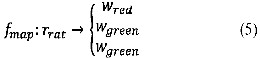
- the weights w red , w green and w blue depend on the ratio value r rat . This may be expressed as follows: f map : r rat ⁇ ⁇ w red w green w green with f map denoting a mapping function used for determining the weights w red , w green and w blue for the primary colors red, green and blue of the color space based on the ratio value r rat .
- a color space such as the RGB color space may be represented using intermediate colors (e.g. yellow, cyan, etc.) by adjusting the weights to create mixed results.
- the pixel structure of the ToF sensor 240 may be non-symmetric such that different offset errors may be introduced into the measurement.
- the offset error may be compensated by an additional measurement.
- the first electrical potential 211 is applied to the first modulation gate 251 and the second electrical potential 212 is applied to the second modulation gate 252 as described above, the signals are switched during another second exposure time for a second measurement.
- the second electrical potential 212 is applied to the first modulation gate 251 during the second exposure time of the ToF sensor 240 and the first electrical potential 211 is applied to the second modulation gate 252. This is done by the driver circuitry 210.
- the received data 259 indicates the first amount of charge collected at the first charge storage of the sensor pixel 240 during the first exposure time and the second amount of charge collected at the second charge storage of the sensor pixel 240 during the first exposure time and additionally a third amount of charge collected at the first charge storage of the sensor pixel 240 during the second exposure time and a fourth amount of charge collected at the second charge storage of the sensor pixel 240 during the second exposure time.
- two color measurements are performed. Using the difference between both measurements may allow to compensate for the offset error.
- a first difference value representing a charge difference between the first amount of charge and the third amount of charge may be determined.
- a second difference value representing a charge difference between the second amount of charge and the fourth amount of charge may be determined.
- the ratio value r rat may accordingly represent the ratio of the first difference value r diff 1 to the second difference value r diff 2 .
- r rat r diff 1 r diff 2
- the color of the light 205 received by the sensor pixel 240 may be determined based on the ratio value r rat analogously to what is described above.
- the above described mapping of the ratio value r rat to a color scale is not the only option for determining the color of the received light 205.
- a variety of classification/mapping schemes may be used.
- the processing circuitry 220 may execute a classification/mapping algorithm for determining the color of the received light 205 based on at least the measured first amount of charge and the measured second amount of charge.
- An alternative approach for determining the color of the received light 205 will be described in the following with reference to Fig. 7 . In the example of Fig. 7 , a plurality of measurements, i.e., a plurality of exposure times are used.
- the first electrical potential 211 is applied to the first modulation gate 251 and the second electrical potential 212 is applied to the second modulation gate 252 of the sensor pixel 250 during the plurality of exposure times of the ToF sensor 240.
- a value of the first electrical potential 211 is equal (i.e. the same, is not changed) for the plurality of exposure times.
- a value of the second electrical potential 212 is different for each of the plurality of exposure times.
- the value of the second electrical potential 212 may be increased or decreased over the plurality of exposure times. In the example of Fig. 7 , the value of the second electrical potential 212 is increased.
- the first electrical potential 211 is higher than the second electrical potential 212 in the example of Fig. 7 .
- the data 259 received indicate the respective first amount of charge collected at the first charge storage of the sensor pixel 250 and the respective second amount of charge collected at the second charge storage of the sensor pixel 250 for the plurality of exposure times.
- the data 259 indicates the respective first amount of charge and the respective second amount of charge for each of the plurality of exposure times (e.g. three or more). This is illustrated in subfigures (a) and (b) of Fig. 7 .
- Fig. 7 illustrates similarly to Fig. 3 in its subfigure (a) the respective first amount of charge collected at the first charge storage (i.e. the readout diode 261) of the sensor pixel 250 for different colors of the received light 205 and for the different values of the second electrical potential 212.
- the curve 710 represents the respective first amount of charge collected at the first charge storage of the sensor pixel 250 for red light.
- the curve 720 represents the respective first amount of charge collected at the first charge storage of the sensor pixel 250 for green light.
- the curve 730 represents the respective first amount of charge collected at the first charge storage of the sensor pixel 250 for blue light.
- Fig. 7 illustrates similarly to Fig. 3 in its subfigure (b) the respective second amount of charge collected at the second charge storage (i.e. the readout diode 262) of the sensor pixel 250 for the different colors of the received light 205 and for the different values of the second electrical potential 212.
- the curve 740 represents the respective second amount of charge collected at the second charge storage of the sensor pixel 250 for the blue light.
- the curve 750 represents the respective second amount of charge collected at the second charge storage of the sensor pixel 250 for the green light.
- the curve 760 represents the respective second amount of charge collected at second first charge storage of the sensor pixel 250 for the red light.
- Fig. 7 illustrates similarly to Fig. 3 in its subfigure (c) the respective ratio of the first amount of charge to the second amount of charge for the different values of the second electrical potential 212.
- the curve 770 represents the respective ratio of the first amount of charge to the second amount of charge for the blue light.
- the curve 780 represents the respective ratio of the first amount of charge to the second amount of charge for the green light.
- the curve 790 represents the respective ratio of the first amount of charge to the second amount of charge for the red light.
- the slopes of the curves 770, 780 and 790 are different from each other. This is exemplarily illustrated by the slopes 775 and 795 of the curves 770 and 790.
- the different slopes of the curves allow to determine the color of the received light 205.
- Determining 108 the color of the light 205 received by the sensor pixel 250 may, hence, comprise determining for the plurality of exposure times a respective ratio value representing a ratio of the respective first amount of charge to the respective second amount of charge as described above and illustrated in subfigure (c) of Fig. 7 .
- a slope (value) of a course of the determined ratio values with respect to the values of the second electrical potential used for the plurality of exposure times may be determined.
- the slope of a curve defined by a plurality of curve points is determined, wherein the curve points are each given by the determined ratio value and the value of the second electrical potential used for the respective exposure time of the plurality of exposure times.
- the determined ratio values are plotted against the values of the second electrical potential used for the plurality of exposure times and a slope of the resulting curve is determined.
- the color of the light 205 received by the sensor pixel 250 may be determined based on the slope (value). For example, it may be determined which of a plurality of value ranges includes the slope (value). Similar to what is described above, each of the value ranges may represent a possible color of the received light 205. Accordingly, the possible color represented by the one of the plurality of value ranges which includes the slope (value) may be determined as the color of the light 205 received by the sensor pixel 250. Alternatively, the slope (value) may be compared to a plurality of reference slopes (slope values). Similar to what is described above, each of the reference slopes (slope values) represents a possible color of the light received by the sensor pixel.
- the possible color represented by the one of the plurality of reference slopes (slope values) that best matches the slope (value) may be determined as the color of the light 205 received by the sensor pixel 250.
- the respective difference between the slope (value) and each of the reference slopes (slope values) may be determined and the possible color represented by the reference slopes (slope values) exhibiting the smallest difference to the slope (value) may be determined as the color of the received light 205.
- the above described value ranges, reference values, reference slopes or mapping functions may be determined based on calibration measurements with the ToF sensor 240.
- at least one of the plurality of value ranges, at least one of the plurality of reference values, a mapping function used for determining the weights for the plurality of primary colors of the color space based on the ratio value or at least one reference slope used for determining the color of the light received by the sensor pixel based on the slope may be determined based on at least one calibration measurement in which the ToF sensor receives predetermined monochromatic light.
- the values r red , r green and r blue used in the example of Figs. 3 and 4 may be determined as follows:
- the received light 205 may be predetermined red light in a first calibration measurement.
- the first electrical potential is applied to the first modulation gate 251 of the sensor pixel 240 during an exposure time of the first calibration measurement.
- the second electrical potential is applied to the second modulation gate 252 of the sensor pixel 240 during the exposure time of the first calibration measurement.
- the first amount of charge C 1 ,cal 1 collected at the first charge storage of the sensor pixel 250 during the exposure time of the first calibration measurement and the second amount of charge C 2, cal 1 collected at the second charge storage of the sensor pixel during 250 the exposure time of the first calibration measurement are determined and analyzed.
- the first electrical potential 211, the second electrical potential 212, the third potential 213, etc. may each be constant during the respective exposure time (i.e. the value of the respective electrical potential is constant / does not change during the respective exposure time). Further, the first electrical potential 211, the second electrical potential 212, the third potential 213, etc. may each be applied continuously during the (whole) respective exposure time.
- one of the first electrical potential 211 and the second electrical potential 212 is ground.
- the other one of the first electrical potential 211 and the second electrical potential 212 is different from ground. If more than two electrical potentials (e.g. third electrical potential 213) are used as the sensor pixel comprises more than two modulation gates, also the other electrical potentials are different from ground.
- each of the first electrical potential 211 and the second electrical potential 212 is different from ground. If more than two electrical potentials (e.g. third electrical potential 213) are used as the sensor pixel comprises more than two modulation gates, also the other electrical potentials are different from ground. Using only electrical potentials different from ground may allow to improve the separation of the charge carriers generated by the received light 205. For example, if the first electrical potential 211 is higher than the second electrical potential 212 and if the second electrical potential 212 is different from ground, more of the generated charge carriers (e.g. electrons or holes) may be sucked into the first charge storage formed by the readout diode 261 compared to a situation in which the second electrical potential 212 is equal to ground. For example, the first electrical potential 211 may be 0.7 V and the second electrical potential 212 may be 0.3 V.
- first electrical potential 211 and the second electrical potential 212 need not be constant potentials.
- a value the first electrical potential 211 may periodically and continuously alternate between a first value and a second value during a respective (single) exposure time of the ToF sensor 240 for the color measurement.
- a value of the second electrical potential 212 may periodically and continuously alternate between the first value and the second value during the respective (single) exposure time of the ToF sensor 240 for the color measurement.
- the values of the first electrical potential 211 and the second electrical potential 212 may alternate periodically and continuously.
- the values of the first electrical potential 211 and the second electrical potential 212 vary inversely between the first value and the second value.
- the value of the first electrical potential 211 changes from the first value to the second value
- the value of the second electrical potential 212 changes from the second value to the first value
- the first value may be 0.7 V and the second value may be between 0 V (i.e. ground) and 0.4 V.
- two continuous wave signals may be applied to the first and second modulation gates 251 and 252, wherein the two continuous wave signals are inverted with respect to each other.
- the third potential 213 applied to the third modulation gate 253 may be constant during the respective exposure time.
- Applying two alternating electrical potentials to the modulation gates 251 and 252 of the sensor pixel 250 may allow to measure the "AC contrast" of the electrons within the sensor pixel 250, whereas applying constant electrical potentials to the modulation gates 251 and 252 of the sensor pixel 250 as described above may allow to measure the "DC contrast” of the electrons within the sensor pixel 250. Irrespective of whether the electrical potentials applied to the modulation gates 251 and 252 are constant or alternate, the charge carriers generated in the semiconductor material 258 of the sensor pixel 250 due to the received light 205 are separated due to the potential difference between the electrical potentials applied to the modulation gates 251 and 252.
- the processing circuitry 220 may further output data indicative of the determined color.
- a color coded image of the scene may be generated and output by the processing circuitry 220.
- the color coded image comprises one or more pixels, wherein one of one or more pixels represents the determined color of the light 205 received by the sensor pixel 250 of the ToF sensor 240.
- the ToF sensor 240 comprises a plurality of sensor pixels
- the color coded image may comprise a plurality of pixels representing the determined colors of the light received by the plurality of sensor pixels of the ToF sensor 240.
- the intensities of the individual pixels may be scaled based on the collected charges. For example, an intensity of the color coded image's pixel may be scaled on the sum of the first amount of charge and the second amount of charge as measured at the sensor pixel 240 for the exposure time.
- the color coded image may be used for image segmentation of a depth image of the scene.
- the ToF sensor 240 may be caused (controlled) to perform at least one ToF measurement of the scene for obtaining a depth image of the scene (e.g. by illuminating the scene with light based on an illumination signal and by driving the modulation gates of the sensor pixel 250 based on a modulated reference signal).
- an image segmentation process may be performed on the depth image for locating one or more objects and/or one or more boundaries in the depth image.
- the image segmentation process uses the color coded image of the scene for locating the one or more objects and/or the one or more boundaries in the depth image.
- the image segmentation using the color coded image of the scene may be done according to conventional techniques.
- the proposed technique for the ToF sensor 240 may allow to capture the depth image and the color coded image with the same image sensor. Accordingly, the depth image and the color coded image are captured with the same angle relative to the scene. Hence, no additional efforts for synchronizing the depth image and the color coded image are needed.
- the RGB camera is not needed such that system costs and system complexity may be reduced.
- Some examples relate to a method for detecting a color of light received from a scene by a ToF sensor.
- the method includes applying a first electrical potential to a first modulation gate of a sensor pixel of the ToF sensor during an exposure time of the ToF sensor. Further, the method includes applying a second electrical potential to a second modulation gate of the sensor pixel during the exposure time. The second electrical potential is different from the first electrical potential.
- the method includes receiving data indicating a first amount of charge collected at a first charge storage of the sensor pixel during the exposure time and a second amount of charge collected at a second charge storage of the sensor pixel during the exposure time. The method further includes determining the color of the light received by the sensor pixel based on the first amount of charge and the second amount of charge.
- determining the color of the light received by the sensor pixel comprises: determining a ratio value representing a ratio of the first amount of charge to the second amount of charge; and determining the color of the light received by the sensor pixel based on the ratio value.
- the method further comprises: applying the second electrical potential to the first modulation gate during another exposure time of the ToF sensor; applying the first electrical potential to the second modulation gate during the other exposure time; and receiving data indicating a third amount of charge collected at the first charge storage during the other exposure time and a fourth amount of charge collected at the second charge storage during the other exposure time, wherein determining the color of the light received by the sensor pixel comprises: determining a first difference value representing a charge difference between the first amount of charge and the third amount of charge; determining a second difference value representing a charge difference between the second amount of charge and the fourth amount of charge; determining a ratio value representing a ratio of the first difference value to the second difference value; and determining the color of the light received by the sensor pixel based on the ratio value.
- determining the color of the light received by the sensor pixel based on the ratio value comprises: determining which of a plurality of value ranges includes the ratio value, each of the value ranges representing a possible color of the light received by the sensor pixel; and determining the possible color represented by the one of the plurality of value ranges which includes the ratio value as the color of the light received by the sensor pixel.
- determining the color of the light received by the sensor pixel based on the ratio value comprises: comparing the ratio value to a plurality of reference values, each of the reference values representing a possible color of the light received by the sensor pixel; and determining the possible color represented by the one of the plurality of reference values that best matches the ratio value as the color of the light received by the sensor pixel.
- determining the color of the light received by the sensor pixel based on the ratio value comprises: determining weights for a plurality of primary colors of a color space based on the ratio value; and combining the plurality of primary colors using the weights for obtaining the color of the light received by the sensor pixel.
- the first electrical potential is applied to the first modulation gate and the second electrical potential is applied to the second modulation gate during a plurality of exposure times of the ToF sensor, wherein a value of the first electrical potential is equal for the plurality of exposure times, wherein a value of the second electrical potential is different for each of the plurality of exposure times, wherein data are received indicating the respective first amount of charge and the respective second amount of charge for the plurality of exposure times, and wherein determining the color of the light received by the sensor pixel based on the first amount of charge and the second amount of charge comprises: determining for the plurality of exposure times a respective ratio value representing a ratio of the respective first amount of charge to the respective second amount of charge; determining a slope of a course of the determined ratio values with respect to the values of the second electrical potential used for the plurality of exposure times; and determining the color of the light received by the sensor pixel based on the slope.
- the method further comprises determining, based on at least one calibration measurement in which the ToF sensor receives predetermined monochromatic light, at least one of the plurality of value ranges, at least one of the plurality of reference values, a mapping function used for determining the weights for the plurality of primary colors of the color space based on the ratio value or at least one reference slope used for determining the color of the light received by the sensor pixel based on the slope.
- the method further comprises generating a color coded image of the scene comprising a pixel representing the determined color of the light received by the sensor pixel of the ToF sensor.
- the method further comprises scaling an intensity of the color coded image's pixel based on a sum of the first amount of charge and the second amount of charge.
- the method further comprises: causing the time-of-flight sensor to perform at least one ToF measurement of the scene for obtaining a depth image of the scene; and performing an image segmentation process on the depth image for locating one or more objects and/or one or more boundaries in the depth image, wherein the image segmentation process uses the color coded image of the scene for locating the one or more objects and/or the one or more boundaries in the depth image.
- the method further comprises applying a third electrical potential to a third modulation gate of the sensor pixel during the exposure time, wherein the third modulation gate is arranged between the first modulation gate and the second modulation gate, and wherein the third electrical potential is between the first electrical potential and the second electrical potential.
- one of the first electrical potential and the second electrical potential is ground.
- each of the first electrical potential and the second electrical potential is different from ground.
- the first electrical potential and the second electrical potential are constant during the exposure time of the ToF sensor.
- a value of the first electrical potential periodically alternates between a first value and a second value during the exposure time of the ToF sensor, wherein a value the second electrical potential periodically alternates between the first value and the second value during the exposure time of the ToF sensor, and wherein the values of the first electrical potential and the second electrical potential vary inversely between the first value and the second value.
- the apparatus comprises driver circuitry configured to apply a first electrical potential to a first modulation gate of a sensor pixel of the ToF sensor during an exposure time of the ToF sensor. Further, the driver circuitry is configured to apply a second electrical potential to a second modulation gate of the sensor pixel during the exposure time. The second electrical potential is different from the first electrical potential.
- the apparatus additionally comprises processing circuitry configured to receive data indicating a first amount of charge collected at a first charge storage of the sensor pixel during the exposure time and a second amount of charge collected at a second charge storage of the sensor pixel during the exposure time. The processing circuitry is further configured to determine the color of the light received by the sensor pixel based on the first amount of charge and the second amount of charge.
- Examples of the present disclosure may enable color sensing with ToF imagers.
- aspects described in relation to a device or system should also be understood as a description of the corresponding method.
- a block, device or functional aspect of the device or system may correspond to a feature, such as a method step, of the corresponding method.
- aspects described in relation to a method shall also be understood as a description of a corresponding block, a corresponding element, a property or a functional feature of a corresponding device or a corresponding system.
Landscapes
- Engineering & Computer Science (AREA)
- Physics & Mathematics (AREA)
- General Physics & Mathematics (AREA)
- Computer Networks & Wireless Communication (AREA)
- Radar, Positioning & Navigation (AREA)
- Remote Sensing (AREA)
- Spectroscopy & Molecular Physics (AREA)
- Color Television Image Signal Generators (AREA)
Abstract
Description
- The present disclosure relates to color sensing with Time-of-Flight (ToF) sensors. In particular, examples relate to a method and an apparatus for detecting a color of light received from a scene by a ToF sensor.
- Color information is used for object segmentation in images of a ToF camera. An RGB camera is conventionally used together with the ToF camera to provide the color information. The images of the ToF camera and the RGB camera have a different angle to the observed scene such that synchronization between both cameras is needed. The combination of the ToF camera and the RGB camera causes high system costs and high system complexity.
- Hence, there may be a demand for color sensing with ToF sensors.
- The demand may be satisfied by the subject matter of the appended claims.
- An example relates to a method for detecting a color of light received from a scene by a ToF sensor. The method includes applying a first electrical potential to a first modulation gate of a sensor pixel of the ToF sensor during an exposure time of the ToF sensor. Further, the method includes applying a second electrical potential to a second modulation gate of the sensor pixel during the exposure time. The second electrical potential is different from the first electrical potential. In addition, the method includes receiving data indicating a first amount of charge collected at a first charge storage of the sensor pixel during the exposure time and a second amount of charge collected at a second charge storage of the sensor pixel during the exposure time. The method further includes determining the color of the light received by the sensor pixel based on the first amount of charge and the second amount of charge.
- Another example relates to an apparatus for detecting a color of light received from a scene by a ToF sensor. The apparatus comprises driver circuitry configured to apply a first electrical potential to a first modulation gate of a sensor pixel of the ToF sensor during an exposure time of the ToF sensor. Further, the driver circuitry is configured to apply a second electrical potential to a second modulation gate of the sensor pixel during the exposure time. The second electrical potential is different from the first electrical potential. The apparatus additionally comprises processing circuitry configured to receive data indicating a first amount of charge collected at a first charge storage of the sensor pixel during the exposure time and a second amount of charge collected at a second charge storage of the sensor pixel during the exposure time. The processing circuitry is further configured to determine the color of the light received by the sensor pixel based on the first amount of charge and the second amount of charge.
- Some examples of apparatuses and/or methods will be described in the following by way of example only, and with reference to the accompanying figures, in which
-
Fig. 1 illustrates a flowchart of an example of a method for detecting a color of light received from a scene by a ToF sensor; -
Fig. 2 illustrates an example of ToF sensor together with an apparatus for detecting a color of light received from a scene by the ToF sensor; -
Fig. 3 illustrates exemplary courses of charges collected at charge storages of a ToF sensor; -
Fig. 4 illustrates an exemplary color spectrum; -
Fig. 5 illustrates exemplary courses of charges collected at charge storages of a ToF sensor; -
Fig. 6 illustrates another exemplary color spectrum; and -
Fig. 7 illustrates exemplary courses of charges collected at charge storages of a ToF sensor. - Some examples are now described in more detail with reference to the enclosed figures. However, other possible examples are not limited to the features of these embodiments described in detail. Other examples may include modifications of the features as well as equivalents and alternatives to the features. Furthermore, the terminology used herein to describe certain examples should not be restrictive of further possible examples.
- Throughout the description of the figures same or similar reference numerals refer to same or similar elements and/or features, which may be identical or implemented in a modified form while providing the same or a similar function. The thickness of lines, layers and/or areas in the figures may also be exaggerated for clarification.
- When two elements A and B are combined using an "or", this is to be understood as disclosing all possible combinations, i.e. only A, only B as well as A and B, unless expressly defined otherwise in the individual case. As an alternative wording for the same combinations, "at least one of A and B" or "A and/or B" may be used. This applies equivalently to combinations of more than two elements.
- If a singular form, such as "a", "an" and "the" is used and the use of only a single element is not defined as mandatory either explicitly or implicitly, further examples may also use several elements to implement the same function. If a function is described below as implemented using multiple elements, further examples may implement the same function using a single element or a single processing entity. It is further understood that the terms "include", "including", "comprise" and/or "comprising", when used, describe the presence of the specified features, integers, steps, operations, processes, elements, components and/or a group thereof, but do not exclude the presence or addition of one or more other features, integers, steps, operations, processes, elements, components and/or a group thereof.
-
Fig. 1 illustrates a flowchart of an example of amethod 100 for detecting a color of light received from a scene by a ToF sensor. Themethod 100 will be described in the following further with reference toFig. 2 which illustrates anexemplary ToF sensor 240 together with anapparatus 200 for detecting a color oflight 205 received from a scene by theToF sensor 240. Contrary to conventional ToF measurements, the scene is not actively illuminated for detecting the color of receivedlight 205. -
Fig. 2 illustrates a sectional view of asensor pixel 250 of theToF sensor 240 along a thickness direction z of theToF sensor 240. TheToF sensor 240 may comprise one or more additional sensor pixels that are analogous to thesensor pixel 250 illustrated inFig. 2 and described in the following. - The
sensor pixel 250, i.e.,ToF sensor 240, comprises a semiconductor material/substrate (e.g. silicon) 258. The receivedlight 205 penetrates thesemiconductor material 258 along the thickness direction z with different depth. In particular, the penetration depth of thelight 205 depends on the wavelength of thelight 205. The longer the wavelength of thelight 205, the deeper the light is able to penetrate theToF sensor 240. - The penetration depth of blue light is rather low such that the blue light is substantially completely absorbed in the upper part of the
semiconductor material 258. This is illustrated inFig. 2 by means of the charge carriers (e.g. electrons or holes) 201 generated in thesemiconductor material 258 by the blue light. Thecharge carriers 201 only occur in the upper part of thesemiconductor material 258. Green light can penetrate thesemiconductor material 258 deeper than blue light. This is illustrated inFig. 2 by means of thecharge carriers 202 generated in thesemiconductor material 258 by the green light. Thecharge carriers 202 occur from the upper to the middle part of thesemiconductor material 258. Red light can penetrate thesemiconductor material 258 deepest. This is illustrated inFig. 2 by means of thecharge carriers 203 generated in thesemiconductor material 258 by the red light. Thecharge carriers 203 are generated in thesemiconductor material 258 from the upper part of thesensor pixel 250 to deep areas at the lower part of thesensor pixel 250. - The wavelength-dependent penetration depth of the
light 205 allows to determine the color of thelight 205. In particular, the electric field within thesensor pixel 250 may be shaped such that the charge carriers generated by the wavelength components of thelight 205 may be separated. The electric field within thesensor pixel 250 depends on the potentials applied to modulation gates (modulation gate terminals) of thesensor pixel 250. In the example ofFig. 2 , thesensor pixel 250 comprises three modulation gates (modulation gate terminals) 251, 252 and 253. It is to be noted that the present disclosure is not limited thereto. In other examples, thesensor pixel 250 may comprise only two modulation gates (e.g. the modulation gate 253 may be omitted). In still other examples, thesensor pixel 250 may comprise more than three modulation gates. In other words, a sensor pixel according to the present disclosure comprises at least two modulation gates. - The
sensor pixel 250 may optionally comprise further terminals such as theseparation terminals Fig. 2 for separating themodulation gates 251, 252 and 253 fromreadout terminals pixel sensor 250. - The
modulation gates 251, 252 and 253 are isolated from thesemiconductor material 258 by an isolation layer (e.g. a thin oxide layer) 259. As described above, the movement of generated charge carriers is controlled by the signals applied to themodulation gates 251, 252 and 253 during an exposure time of the ToF sensor. Accordingly, a transport of the generated charged carriers to the left or to the right side of thesensor pixel 250 may be influenced. - The
method 100 comprises applying 102 a firstelectrical potential 211 to thefirst modulation gate 251 during a (single) exposure time of theToF sensor 240. Additionally, themethod 100 comprises applying 104 a secondelectrical potential 212 to the second modulation gate 252 during the exposure time. Theapparatus 200 comprisesdriver circuitry 210 coupled to thefirst modulation gate 251 as well as the second modulation gate 252 and configured to apply the respective electrical potential. The firstelectrical potential 211 and the secondelectrical potential 212 may be constant potentials. Further, the firstelectrical potential 211 and the secondelectrical potential 212 may be continuously applied to the respective one of thefirst modulation gate 251 and the second modulation gate 252 during the exposure time. - Similarly, the
driver circuitry 210 may be configured to apply a thirdelectrical potential 213 to the third modulation gate 253. As the third modulation gate 253 is arranged between thefirst modulation gate 251 and the second modulation gate 252 along a lateral extension of thesensor pixel 250, the thirdelectrical potential 213 is between the firstelectrical potential 211 and the secondelectrical potential 212. In other words, the thirdelectrical potential 213 is an intermediate potential. - For example, if the first
electrical potential 211 is higher than the secondelectrical potential 212, generated electrons may substantially travel to the right side of thesensor pixel 250 and accumulate near thereadout terminal 257. Only a few generated electrons may travel to the left side of thesensor pixel 250 and accumulate near thereadout terminal 256.Readout diodes readout terminals readout terminals readout diodes readout terminal 256 is coupled to a first charge storage formed by thereadout diode 261, whereas thereadout terminal 257 is coupled to a second charge storage formed by thereadout diode 262. It is to be noted that instead of n+ regions in a p-dopedsemiconductor material 258, p+ regions in an n-dopedsemiconductor material 258 may be used alternatively. - Accordingly, the readout signal provided by the
readout terminal 256 indicates a first amount of charge collected at the first charge storage of thesensor pixel 250 during the exposure time. Similarly, the readout signal provided by thereadout terminal 257 indicates a second amount of charge collected at the second charge storage of thesensor pixel 250 during the exposure time. - The
readout terminals processing circuitry 220 of theapparatus 200 in the example ofFig. 2 such that theprocessing circuitry 220 receives readout signals from thereadout terminals readout terminals ToF sensor 240. Accordingly, various types and numbers of signals may be provided from theToF sensor 240 to theprocessing circuitry 220 for informing theprocessing circuitry 220 about the charges collected at the charge storages of thesensor pixel 250 during the exposure time. In general, theprocessing circuitry 220 is configured to receive data 259 (e.g. encoded to one or more signals) indicating the first amount of charge collected at the first charge storage of thesensor pixel 250 during the exposure time and the second amount of charge collected at the second charge storage of thesensor pixel 250 during the exposure time. Analogously, themethod 100 comprises receiving 106 data indicating the first amount of charge collected at the first charge storage of thesensor pixel 250 during the exposure time and the second amount of charge collected at the second charge storage of thesensor pixel 250 during the exposure time. - In the example of
Fig. 2 , theprocessing circuitry 220 is illustrates as separate circuitry external to theToF sensor 240. However, it is to be noted that the present disclosure is not limited thereto. In alternative examples, theToF sensor 240 may comprise theprocessing circuitry 220. In other words, theprocessing circuitry 220 may be an integral part of theToF sensor 240 such that thedata 259 are processed within theToF sensor 240. - The first amount of charge collected at the first charge storage of the
sensor pixel 250 compared to the second amount of charge collected at the second charge storage of thesensor pixel 240 during the exposure time depends on the color of the received light 205 due to the wavelength-dependent penetration depth of the light 205. - Accordingly, the
method 100 comprises determining 108 the color of the light 205 received by thesensor pixel 240 based on the first amount of charge and the second amount of charge. Theprocessing circuitry 220 is accordingly configured to determine the color of the light 205 received by thesensor pixel 240 based on the first amount of charge and the second amount of charge. -
Fig. 3 exemplarily illustrates how the first amount of charge and the second amount of charge depend on the wavelength of the light 205. The abscissa in each of subfigures (a) to (c) ofFig. 3 denotes the value of the firstelectrical potential 211 used during the exposure time of theToF sensor 240 in arbitrary units. The firstelectrical potential 211 is higher than the secondelectrical potential 212 in the example ofFig. 3 and not changed. In other words, the secondelectrical potential 212 is the same for each data point in the example ofFig. 3 . -
Fig. 3 illustrates in subfigure (a) the respective first amount of charge collected at the first charge storage (i.e. the readout diode 261) of thesensor pixel 250 for different colors of the received light 205 and for the different values of the firstelectrical potential 211. The ordinate denotes the first amount of charge in arbitrary units. Thecurve 310 represents the respective first amount of charge collected at the first charge storage of thesensor pixel 250 for red light. Thecurve 320 represents the respective first amount of charge collected at the first charge storage of thesensor pixel 250 for green light. Thecurve 330 represents the respective first amount of charge collected at the first charge storage of thesensor pixel 250 for blue light. As can be seen from subfigure (a), the first amount of charge collected at the first charge storage is different for red, green and blue light. Further, subfigure (a) illustrates that the first amount of charge decreases if the value of the firstelectrical potential 211 is increased. When comparing thecurves light 205. - Subfigure (b) of
Fig. 3 illustrates the respective second amount of charge collected at the second charge storage (i.e. the readout diode 262) of thesensor pixel 250 for the different colors of the received light 205 and for the different values of the firstelectrical potential 211. The ordinate denotes the second amount of charge in arbitrary units. Thecurve 340 represents the respective second amount of charge collected at the second charge storage of thesensor pixel 250 for the red light. Thecurve 350 represents the respective second amount of charge collected at the second charge storage of thesensor pixel 250 for the green light. Thecurve 360 represents the respective second amount of charge collected at second first charge storage of thesensor pixel 250 for the blue light. As can be seen from subfigure (b), the second amount of charge collected at the second charge storage is different for red, green and blue light. Further, subfigure (b) illustrates that the second amount of charge increases if the value of the firstelectrical potential 211 is increased. When comparing thecurves light 205. - When comparing the corresponding curves in subfigures (a) and (b), it is evident that the respective second amount of charge is significantly smaller than the respective first amount of charge for each of the colors. As the first
electrical potential 211 is higher than thesecond potential 212, most electrons generated by the received light 205 in thesemiconductor material 258 of thesensor pixel 250 travel to thereadout diode 261 at the right side and are, hence, collected in the first charge storage. A comparatively small amount of the generated electrons travels to thereadout diode 262 at the left side and is, hence, collected in the second charge storage. -
Fig. 3 illustrates in subfigure (c) the respective ratio of the first amount of charge to the second amount of charge for the different values of the firstelectrical potential 211. The ordinate denotes the respective ratio value. Thecurve 370 represents the respective ratio of the first amount of charge to the second amount of charge for the blue light. Thecurve 380 represents the respective ratio of the first amount of charge to the second amount of charge for the green light. Thecurve 390 represents the respective ratio of the first amount of charge to the second amount of charge for the red light. - As can be seen from subfigure (c), the ratio of the first amount of charge to the second amount of charge increases for each of the colors if the value of the first
electrical potential 211 is increased. However, the relation between the ratios for the different colors stay substantially constant irrespective of the value of the firstelectrical potential 211. As illustrated inFig. 3 , the ratio of the first amount of charge to the second amount of charge is higher for blue light than for green light irrespective of the value of the firstelectrical potential 211. Similarly, the ratio of the first amount of charge to the second amount of charge is higher for green light than for red light irrespective of the value of the firstelectrical potential 211. - This behavior of the ratio of the first amount of charge to the second amount of charge allows to determine the color of the light 205.
- Determining 108 the color of the light 205 received by the
sensor pixel 250 may, hence, comprise determining a ratio value (e.g. as illustrated in subfigure (c) ofFig. 3 ) representing a ratio of the first amount of charge (e.g. as illustrated in subfigure (a) ofFig. 3 ) to the second amount of charge (e.g. as illustrated in subfigure (b) ofFig. 3 ). Further, the determining 108 the color of the light 205 received by thesensor pixel 250 may comprise determining the color of the light 205 received by thesensor pixel 250 based on the ratio value as the ratio value is characteristic for the color of the light 205. In other words, the information stored in the charge storage elements of thesensor pixel 250 is sampled. The sampled values are divided. The ratio of these values indicates the sensed color. The ratio may be fitted to a color scale as will be described in the following. - As can be seen from
Fig. 3 , the ratio of the first amount of charge to the second amount of charge is within a certain value range for each color and for each value of the firstelectrical potential 211. This may be used for determining the color of the light 205. - For example, determining 108 the color of the light received by the sensor pixel based on the ratio value may comprise determining which of a plurality of value ranges includes the ratio value representing the ratio of the first amount of charge to the second amount of charge. Each of the value ranges represents a possible color of the light received by the sensor pixel such as red, green or blue. Accordingly, the possible color represented by the one of the plurality of value ranges which includes the ratio value may be determined as the color of the light received by the sensor pixel.
- This is exemplarily illustrated in
Fig. 4 illustrating three value ranges 410, 420 and 420 used for mapping the ratio value rrat to an exemplary color spectrum which comprises three colors. Thevalue range 410 represents red, thevalue range 420 represents green and thevalue range 410 represents blue. - The
value range 410 is bounded by the values rred and
value range 420 is bounded by the values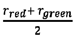

value range 420 is bounded by the values
- The classification of the ratio value rrat may be done as follows:


- 1 denotes in mathematical expressions (1) to (3) that the ratio value rrat is within the respective value range and that the color of the received light 205 is, hence, the possible color represented by the respective value range. 0 denotes in mathematical expressions (1) to (3) that the ratio value rrat is not within the value range and that the color of the received light 205 is, hence, not the possible color represented by the respective value range. In other words, the ratio value rrat is fitted to a color space by means of a threshold comparison.
- However, it is to be noted that the value ranges of
Fig. 4 are merely exemplary. More or less value ranges may be used to decrease or increase the granularity of the color mapping. This is exemplarily illustrated inFigs. 5 and6 .Fig. 5 illustrates similarly toFig. 3 in its subfigure (a) the respective first amount of charge collected at the first charge storage (i.e. the readout diode 261) of thesensor pixel 250 for different colors of the received light 205 and for the different values of the firstelectrical potential 211. In addition to thecurves Fig. 5 further illustrates thecurves Fig. 5 illustrates similarly toFig. 3 in its subfigure (b) the respective second amount of charge collected at the second charge storage (i.e. the readout diode 262) of thesensor pixel 250 for the different colors of the received light 205 and for the different values of the firstelectrical potential 211. In addition to thecurves Fig. 5 further illustrates thecurves Fig. 5 illustrates similarly toFig. 3 in its subfigure (c) the respective ratio of the first amount of charge to the second amount of charge. In addition to thecurves Fig. 5 further illustrates thecurves - Further illustrated in
Fig. 5 is a gray scale representation of acolor spectrum 500 to which the determined ratio value may be mapped.Fig. 6 illustrates the gray scale representation of thecolor spectrum 500 with more details. In comparison to the example ofFig. 4 , thecolor spectrum 500 comprises not only red, green and blue but also gradations, i.e. mixtures of red, green and blue. As a reference, the values rred ,

Fig. 6 . For example, value ranges for red, orange, yellow, green, cyan and blue may be defined and used for the comparison such that the color of the received light 205 may be determined with higher granularity. - Alternatively, reference values representing a respective possible color of the receive light 205 may be defined and used instead of the value ranges. For example, reference values may be defined for different shades/tones of red, orange, yellow, green, blue etc. Accordingly, determining 108 the color of the light received by the sensor pixel based on the ratio value may comprise comparing the ratio value to a plurality of reference values. As described above, each of the reference values represents a possible color of the light 205 received by the
sensor pixel 250. The possible color represented by the one of the plurality of reference values that best matches the ratio value may be determined as the color of the light 205 received by thesensor pixel 250. For example, the respective difference between the ratio value and each of the reference values may be determined and the possible color represented by the reference value exhibiting the smallest difference to the ratio value may be determined as the color of the receivedlight 205. - In other examples, a plurality of primary colors (e.g. red, green and blue) may be mixed, wherein the mixing ratios are determined based on the ratio value. This may allow a more complex color mapping. Accordingly, determining 108 the color of the light 205 received by the
sensor pixel 250 may comprise determining weights for a plurality of primary colors of a color space based on the ratio value and combining the plurality of primary colors using the weights for obtaining the color of the receivedlight 205. The weights determine (describe) the intensities of the primary colors such that the color of the received light 205 is a mixture of the intensities of the primary colors. - For example, if red, green and blue are the primary colors of an exemplary color space, they may be combined as follows for obtaining the color C of the received light 205:

- The weights wred, wgreen and wblue depend on the ratio value rrat . This may be expressed as follows:
- For example, similar to the example of
Fig. 4 , the weights wred, wgreen and wblue may be set either to 0 or 1 depending on the ratio value rrat :


- In other examples, a color space such as the RGB color space may be represented using intermediate colors (e.g. yellow, cyan, etc.) by adjusting the weights to create mixed results. In the following example, the intermediate colors yellow and cyan are used for the RGB color space:


- In this examples, the weights wred, wgreen and wblue are set as follows depending on the ratio value rrat :


- However, it is to be noted that the above examples are merely exemplary. More or less and/or different primary colors may be used. Similarly, the weighted primary colors may be combined differently.
- The pixel structure of the
ToF sensor 240 may be non-symmetric such that different offset errors may be introduced into the measurement. The offset error may be compensated by an additional measurement. - While during the first exposure for the first measurement, the first
electrical potential 211 is applied to thefirst modulation gate 251 and the secondelectrical potential 212 is applied to the second modulation gate 252 as described above, the signals are switched during another second exposure time for a second measurement. In other words, the secondelectrical potential 212 is applied to thefirst modulation gate 251 during the second exposure time of theToF sensor 240 and the firstelectrical potential 211 is applied to the second modulation gate 252. This is done by thedriver circuitry 210. - Accordingly, the received
data 259 indicates the first amount of charge collected at the first charge storage of thesensor pixel 240 during the first exposure time and the second amount of charge collected at the second charge storage of thesensor pixel 240 during the first exposure time and additionally a third amount of charge collected at the first charge storage of thesensor pixel 240 during the second exposure time and a fourth amount of charge collected at the second charge storage of thesensor pixel 240 during the second exposure time. In other words, two color measurements are performed. Using the difference between both measurements may allow to compensate for the offset error. - Accordingly, a first difference value representing a charge difference between the first amount of charge and the third amount of charge may be determined. Similarly, a second difference value representing a charge difference between the second amount of charge and the fourth amount of charge may be determined.
- The ratio value rrat may accordingly represent the ratio of the first difference value r diff1 to the second difference value r diff2. In other words:

- The color of the light 205 received by the
sensor pixel 240 may be determined based on the ratio value rrat analogously to what is described above. - The above described mapping of the ratio value rrat to a color scale is not the only option for determining the color of the received
light 205. A variety of classification/mapping schemes may be used. For example, theprocessing circuitry 220 may execute a classification/mapping algorithm for determining the color of the received light 205 based on at least the measured first amount of charge and the measured second amount of charge. An alternative approach for determining the color of the received light 205 will be described in the following with reference toFig. 7 . In the example ofFig. 7 , a plurality of measurements, i.e., a plurality of exposure times are used. - Similar to what is described above, the first
electrical potential 211 is applied to thefirst modulation gate 251 and the secondelectrical potential 212 is applied to the second modulation gate 252 of thesensor pixel 250 during the plurality of exposure times of theToF sensor 240. A value of the firstelectrical potential 211 is equal (i.e. the same, is not changed) for the plurality of exposure times. A value of the secondelectrical potential 212 is different for each of the plurality of exposure times. For example, the value of the secondelectrical potential 212 may be increased or decreased over the plurality of exposure times. In the example ofFig. 7 , the value of the secondelectrical potential 212 is increased. The firstelectrical potential 211 is higher than the secondelectrical potential 212 in the example ofFig. 7 . - Accordingly, the
data 259 received indicate the respective first amount of charge collected at the first charge storage of thesensor pixel 250 and the respective second amount of charge collected at the second charge storage of thesensor pixel 250 for the plurality of exposure times. For example, thedata 259 indicates the respective first amount of charge and the respective second amount of charge for each of the plurality of exposure times (e.g. three or more). This is illustrated in subfigures (a) and (b) ofFig. 7 . -
Fig. 7 illustrates similarly toFig. 3 in its subfigure (a) the respective first amount of charge collected at the first charge storage (i.e. the readout diode 261) of thesensor pixel 250 for different colors of the received light 205 and for the different values of the secondelectrical potential 212. Thecurve 710 represents the respective first amount of charge collected at the first charge storage of thesensor pixel 250 for red light. Thecurve 720 represents the respective first amount of charge collected at the first charge storage of thesensor pixel 250 for green light. Thecurve 730 represents the respective first amount of charge collected at the first charge storage of thesensor pixel 250 for blue light. - Further,
Fig. 7 illustrates similarly toFig. 3 in its subfigure (b) the respective second amount of charge collected at the second charge storage (i.e. the readout diode 262) of thesensor pixel 250 for the different colors of the received light 205 and for the different values of the secondelectrical potential 212. Thecurve 740 represents the respective second amount of charge collected at the second charge storage of thesensor pixel 250 for the blue light. Thecurve 750 represents the respective second amount of charge collected at the second charge storage of thesensor pixel 250 for the green light. Thecurve 760 represents the respective second amount of charge collected at second first charge storage of thesensor pixel 250 for the red light. - Still further,
Fig. 7 illustrates similarly toFig. 3 in its subfigure (c) the respective ratio of the first amount of charge to the second amount of charge for the different values of the secondelectrical potential 212. Thecurve 770 represents the respective ratio of the first amount of charge to the second amount of charge for the blue light. Thecurve 780 represents the respective ratio of the first amount of charge to the second amount of charge for the green light. Thecurve 790 represents the respective ratio of the first amount of charge to the second amount of charge for the red light. - As can be seen from subfigure (c), the slopes of the
curves slopes curves light 205. - Determining 108 the color of the light 205 received by the
sensor pixel 250 may, hence, comprise determining for the plurality of exposure times a respective ratio value representing a ratio of the respective first amount of charge to the respective second amount of charge as described above and illustrated in subfigure (c) ofFig. 7 . - Further, a slope (value) of a course of the determined ratio values with respect to the values of the second electrical potential used for the plurality of exposure times may be determined. In other words, the slope of a curve defined by a plurality of curve points is determined, wherein the curve points are each given by the determined ratio value and the value of the second electrical potential used for the respective exposure time of the plurality of exposure times. As illustrated in subfigure (c) of
Fig. 7 , the determined ratio values are plotted against the values of the second electrical potential used for the plurality of exposure times and a slope of the resulting curve is determined. - As the slope is color dependent, the color of the light 205 received by the
sensor pixel 250 may be determined based on the slope (value). For example, it may be determined which of a plurality of value ranges includes the slope (value). Similar to what is described above, each of the value ranges may represent a possible color of the receivedlight 205. Accordingly, the possible color represented by the one of the plurality of value ranges which includes the slope (value) may be determined as the color of the light 205 received by thesensor pixel 250. Alternatively, the slope (value) may be compared to a plurality of reference slopes (slope values). Similar to what is described above, each of the reference slopes (slope values) represents a possible color of the light received by the sensor pixel. The possible color represented by the one of the plurality of reference slopes (slope values) that best matches the slope (value) may be determined as the color of the light 205 received by thesensor pixel 250. For example, the respective difference between the slope (value) and each of the reference slopes (slope values) may be determined and the possible color represented by the reference slopes (slope values) exhibiting the smallest difference to the slope (value) may be determined as the color of the receivedlight 205. - The above described value ranges, reference values, reference slopes or mapping functions may be determined based on calibration measurements with the
ToF sensor 240. According to examples, at least one of the plurality of value ranges, at least one of the plurality of reference values, a mapping function used for determining the weights for the plurality of primary colors of the color space based on the ratio value or at least one reference slope used for determining the color of the light received by the sensor pixel based on the slope may be determined based on at least one calibration measurement in which the ToF sensor receives predetermined monochromatic light. - For example, the values rred, rgreen and rblue used in the example of
Figs. 3 and4 may be determined as follows: For determining rred, the received light 205 may be predetermined red light in a first calibration measurement. Similar to what is described above, the first electrical potential is applied to thefirst modulation gate 251 of thesensor pixel 240 during an exposure time of the first calibration measurement. Analogously, the second electrical potential is applied to the second modulation gate 252 of thesensor pixel 240 during the exposure time of the first calibration measurement. The first amount of charge C 1,cal1 collected at the first charge storage of thesensor pixel 250 during the exposure time of the first calibration measurement and the second amount of charge C 2,cal1 collected at the second charge storage of the sensor pixel during 250 the exposure time of the first calibration measurement are determined and analyzed. The value red is determined based on the ratio of the measurement amounts of charge as follows:
- Analogously, a second calibration measurement with predetermined green light may be performed for determining the value rgreen :

sensor pixel 250 during the exposure time of the second calibration measurement. - A third calibration measurement with predetermined blue light may be performed for determining the value rblue:

sensor pixel 250 during the exposure time of the third calibration measurement. - While measuring a color and/or while performing a calibration measurement, the first
electrical potential 211, the secondelectrical potential 212, thethird potential 213, etc. may each be constant during the respective exposure time (i.e. the value of the respective electrical potential is constant / does not change during the respective exposure time). Further, the firstelectrical potential 211, the secondelectrical potential 212, thethird potential 213, etc. may each be applied continuously during the (whole) respective exposure time. - In some examples, one of the first
electrical potential 211 and the secondelectrical potential 212 is ground. The other one of the firstelectrical potential 211 and the secondelectrical potential 212 is different from ground. If more than two electrical potentials (e.g. third electrical potential 213) are used as the sensor pixel comprises more than two modulation gates, also the other electrical potentials are different from ground. - In other examples, each of the first
electrical potential 211 and the secondelectrical potential 212 is different from ground. If more than two electrical potentials (e.g. third electrical potential 213) are used as the sensor pixel comprises more than two modulation gates, also the other electrical potentials are different from ground. Using only electrical potentials different from ground may allow to improve the separation of the charge carriers generated by the receivedlight 205. For example, if the firstelectrical potential 211 is higher than the secondelectrical potential 212 and if the secondelectrical potential 212 is different from ground, more of the generated charge carriers (e.g. electrons or holes) may be sucked into the first charge storage formed by thereadout diode 261 compared to a situation in which the secondelectrical potential 212 is equal to ground. For example, the firstelectrical potential 211 may be 0.7 V and the secondelectrical potential 212 may be 0.3 V. - It is to be noted that the first
electrical potential 211 and the secondelectrical potential 212 need not be constant potentials. In some examples, a value the firstelectrical potential 211 may periodically and continuously alternate between a first value and a second value during a respective (single) exposure time of theToF sensor 240 for the color measurement. In this example, also a value of the secondelectrical potential 212 may periodically and continuously alternate between the first value and the second value during the respective (single) exposure time of theToF sensor 240 for the color measurement. Also during a calibration measurement, the values of the firstelectrical potential 211 and the secondelectrical potential 212 may alternate periodically and continuously. The values of the firstelectrical potential 211 and the secondelectrical potential 212 vary inversely between the first value and the second value. That is, when the value of the first electrical potential 211 changes from the first value to the second value, the value of the second electrical potential 212 changes from the second value to the first value, and vice versa. For example, the first value may be 0.7 V and the second value may be between 0 V (i.e. ground) and 0.4 V. In other words, two continuous wave signals (that oscillate between two signal levels/values) may be applied to the first andsecond modulation gates 251 and 252, wherein the two continuous wave signals are inverted with respect to each other. The third potential 213 applied to the third modulation gate 253 may be constant during the respective exposure time. - Applying two alternating electrical potentials to the
modulation gates 251 and 252 of thesensor pixel 250 may allow to measure the "AC contrast" of the electrons within thesensor pixel 250, whereas applying constant electrical potentials to themodulation gates 251 and 252 of thesensor pixel 250 as described above may allow to measure the "DC contrast" of the electrons within thesensor pixel 250. Irrespective of whether the electrical potentials applied to themodulation gates 251 and 252 are constant or alternate, the charge carriers generated in thesemiconductor material 258 of thesensor pixel 250 due to the received light 205 are separated due to the potential difference between the electrical potentials applied to themodulation gates 251 and 252. - The
processing circuitry 220 may further output data indicative of the determined color. For example, a color coded image of the scene may be generated and output by theprocessing circuitry 220. The color coded image comprises one or more pixels, wherein one of one or more pixels represents the determined color of the light 205 received by thesensor pixel 250 of theToF sensor 240. For example, if theToF sensor 240 comprises a plurality of sensor pixels, the color coded image may comprise a plurality of pixels representing the determined colors of the light received by the plurality of sensor pixels of theToF sensor 240. - In order to provide a uniform intensity among the pixels of the color coded image of the scene, the intensities of the individual pixels may be scaled based on the collected charges. For example, an intensity of the color coded image's pixel may be scaled on the sum of the first amount of charge and the second amount of charge as measured at the
sensor pixel 240 for the exposure time. - The color coded image may be used for image segmentation of a depth image of the scene. For example, the
ToF sensor 240 may be caused (controlled) to perform at least one ToF measurement of the scene for obtaining a depth image of the scene (e.g. by illuminating the scene with light based on an illumination signal and by driving the modulation gates of thesensor pixel 250 based on a modulated reference signal). Subsequently, an image segmentation process may be performed on the depth image for locating one or more objects and/or one or more boundaries in the depth image. The image segmentation process uses the color coded image of the scene for locating the one or more objects and/or the one or more boundaries in the depth image. The image segmentation using the color coded image of the scene may be done according to conventional techniques. Compared to conventional system architectures using a separate RGB camera for obtaining a color coded image of the scene, the proposed technique for theToF sensor 240 may allow to capture the depth image and the color coded image with the same image sensor. Accordingly, the depth image and the color coded image are captured with the same angle relative to the scene. Hence, no additional efforts for synchronizing the depth image and the color coded image are needed. Compared to conventional system architectures using a separate RGB camera for obtaining a color coded image of the scene, the RGB camera is not needed such that system costs and system complexity may be reduced. - The examples as described herein may be summarized as follows:
Some examples relate to a method for detecting a color of light received from a scene by a ToF sensor. The method includes applying a first electrical potential to a first modulation gate of a sensor pixel of the ToF sensor during an exposure time of the ToF sensor. Further, the method includes applying a second electrical potential to a second modulation gate of the sensor pixel during the exposure time. The second electrical potential is different from the first electrical potential. In addition, the method includes receiving data indicating a first amount of charge collected at a first charge storage of the sensor pixel during the exposure time and a second amount of charge collected at a second charge storage of the sensor pixel during the exposure time. The method further includes determining the color of the light received by the sensor pixel based on the first amount of charge and the second amount of charge. - According to some examples, determining the color of the light received by the sensor pixel comprises: determining a ratio value representing a ratio of the first amount of charge to the second amount of charge; and determining the color of the light received by the sensor pixel based on the ratio value.
- In alternative examples, the method further comprises: applying the second electrical potential to the first modulation gate during another exposure time of the ToF sensor; applying the first electrical potential to the second modulation gate during the other exposure time; and receiving data indicating a third amount of charge collected at the first charge storage during the other exposure time and a fourth amount of charge collected at the second charge storage during the other exposure time, wherein determining the color of the light received by the sensor pixel comprises: determining a first difference value representing a charge difference between the first amount of charge and the third amount of charge; determining a second difference value representing a charge difference between the second amount of charge and the fourth amount of charge; determining a ratio value representing a ratio of the first difference value to the second difference value; and determining the color of the light received by the sensor pixel based on the ratio value.
- According to some examples, determining the color of the light received by the sensor pixel based on the ratio value comprises: determining which of a plurality of value ranges includes the ratio value, each of the value ranges representing a possible color of the light received by the sensor pixel; and determining the possible color represented by the one of the plurality of value ranges which includes the ratio value as the color of the light received by the sensor pixel.
- In alternative examples, determining the color of the light received by the sensor pixel based on the ratio value comprises: comparing the ratio value to a plurality of reference values, each of the reference values representing a possible color of the light received by the sensor pixel; and determining the possible color represented by the one of the plurality of reference values that best matches the ratio value as the color of the light received by the sensor pixel.
- In further alternative examples, determining the color of the light received by the sensor pixel based on the ratio value comprises: determining weights for a plurality of primary colors of a color space based on the ratio value; and combining the plurality of primary colors using the weights for obtaining the color of the light received by the sensor pixel.
- In some examples, the first electrical potential is applied to the first modulation gate and the second electrical potential is applied to the second modulation gate during a plurality of exposure times of the ToF sensor, wherein a value of the first electrical potential is equal for the plurality of exposure times, wherein a value of the second electrical potential is different for each of the plurality of exposure times, wherein data are received indicating the respective first amount of charge and the respective second amount of charge for the plurality of exposure times, and wherein determining the color of the light received by the sensor pixel based on the first amount of charge and the second amount of charge comprises: determining for the plurality of exposure times a respective ratio value representing a ratio of the respective first amount of charge to the respective second amount of charge; determining a slope of a course of the determined ratio values with respect to the values of the second electrical potential used for the plurality of exposure times; and determining the color of the light received by the sensor pixel based on the slope.
- According to some examples, the method further comprises determining, based on at least one calibration measurement in which the ToF sensor receives predetermined monochromatic light, at least one of the plurality of value ranges, at least one of the plurality of reference values, a mapping function used for determining the weights for the plurality of primary colors of the color space based on the ratio value or at least one reference slope used for determining the color of the light received by the sensor pixel based on the slope.
- In some examples, the method further comprises generating a color coded image of the scene comprising a pixel representing the determined color of the light received by the sensor pixel of the ToF sensor.
- According to some examples, the method further comprises scaling an intensity of the color coded image's pixel based on a sum of the first amount of charge and the second amount of charge.
- In some examples, the method further comprises: causing the time-of-flight sensor to perform at least one ToF measurement of the scene for obtaining a depth image of the scene; and performing an image segmentation process on the depth image for locating one or more objects and/or one or more boundaries in the depth image, wherein the image segmentation process uses the color coded image of the scene for locating the one or more objects and/or the one or more boundaries in the depth image.
- According to some examples, the method further comprises applying a third electrical potential to a third modulation gate of the sensor pixel during the exposure time, wherein the third modulation gate is arranged between the first modulation gate and the second modulation gate, and wherein the third electrical potential is between the first electrical potential and the second electrical potential.
- In some examples, one of the first electrical potential and the second electrical potential is ground.
- According to some examples, each of the first electrical potential and the second electrical potential is different from ground.
- In some example, the first electrical potential and the second electrical potential are constant during the exposure time of the ToF sensor.
- In alternative examples, a value of the first electrical potential periodically alternates between a first value and a second value during the exposure time of the ToF sensor, wherein a value the second electrical potential periodically alternates between the first value and the second value during the exposure time of the ToF sensor, and wherein the values of the first electrical potential and the second electrical potential vary inversely between the first value and the second value.
- Other examples relate to an apparatus for detecting a color of light received from a scene by a ToF sensor. The apparatus comprises driver circuitry configured to apply a first electrical potential to a first modulation gate of a sensor pixel of the ToF sensor during an exposure time of the ToF sensor. Further, the driver circuitry is configured to apply a second electrical potential to a second modulation gate of the sensor pixel during the exposure time. The second electrical potential is different from the first electrical potential. The apparatus additionally comprises processing circuitry configured to receive data indicating a first amount of charge collected at a first charge storage of the sensor pixel during the exposure time and a second amount of charge collected at a second charge storage of the sensor pixel during the exposure time. The processing circuitry is further configured to determine the color of the light received by the sensor pixel based on the first amount of charge and the second amount of charge.
- Examples of the present disclosure may enable color sensing with ToF imagers.
- The aspects and features described in relation to a particular one of the previous examples may also be combined with one or more of the further examples to replace an identical or similar feature of that further example or to additionally introduce the features into the further example.
- It is further understood that the disclosure of several steps, processes, operations or functions disclosed in the description or claims shall not be construed to imply that these operations are necessarily dependent on the order described, unless explicitly stated in the individual case or necessary for technical reasons. Therefore, the previous description does not limit the execution of several steps or functions to a certain order. Furthermore, in further examples, a single step, function, process or operation may include and/or be broken up into several sub-steps, - functions, -processes or -operations.
- If some aspects have been described in relation to a device or system, these aspects should also be understood as a description of the corresponding method. For example, a block, device or functional aspect of the device or system may correspond to a feature, such as a method step, of the corresponding method. Accordingly, aspects described in relation to a method shall also be understood as a description of a corresponding block, a corresponding element, a property or a functional feature of a corresponding device or a corresponding system.
- The following claims are hereby incorporated in the detailed description, wherein each claim may stand on its own as a separate example. It should also be noted that although in the claims a dependent claim refers to a particular combination with one or more other claims, other examples may also include a combination of the dependent claim with the subject matter of any other dependent or independent claim. Such combinations are hereby explicitly proposed, unless it is stated in the individual case that a particular combination is not intended. Furthermore, features of a claim should also be included for any other independent claim, even if that claim is not directly defined as dependent on that other independent claim.
Claims (15)
- A method (100) for detecting a color of light received from a scene by a Time-of-Flight, ToF, sensor, the method (100) comprising:applying (102) a first electrical potential to a first modulation gate of a sensor pixel of the ToF sensor during an exposure time of the ToF sensor;applying (104) a second electrical potential to a second modulation gate of the sensor pixel during the exposure time, wherein the second electrical potential is different from the first electrical potential;receiving (106) data indicating a first amount of charge collected at a first charge storage of the sensor pixel during the exposure time and a second amount of charge collected at a second charge storage of the sensor pixel during the exposure time; anddetermining (108) the color of the light received by the sensor pixel based on the first amount of charge and the second amount of charge.
- The method (100) of claim 1, wherein determining (108) the color of the light received by the sensor pixel comprises:determining a ratio value representing a ratio of the first amount of charge to the second amount of charge; anddetermining the color of the light received by the sensor pixel based on the ratio value.
- The method (100) of claim 1, further comprising:applying the second electrical potential to the first modulation gate during another exposure time of the ToF sensor;applying the first electrical potential to the second modulation gate during the other exposure time; andreceiving data indicating a third amount of charge collected at the first charge storage during the other exposure time and a fourth amount of charge collected at the second charge storage during the other exposure time,wherein determining (108) the color of the light received by the sensor pixel comprises:determining a first difference value representing a charge difference between the first amount of charge and the third amount of charge;determining a second difference value representing a charge difference between the second amount of charge and the fourth amount of charge;determining a ratio value representing a ratio of the first difference value to the second difference value; anddetermining the color of the light received by the sensor pixel based on the ratio value.
- The method (100) of claim 2 or claim 3, wherein determining the color of the light received by the sensor pixel based on the ratio value comprises:determining which of a plurality of value ranges includes the ratio value, each of the value ranges representing a possible color of the light received by the sensor pixel; anddetermining the possible color represented by the one of the plurality of value ranges which includes the ratio value as the color of the light received by the sensor pixel.
- The method (100) of claim 2 or claim 3, wherein determining the color of the light received by the sensor pixel based on the ratio value comprises:comparing the ratio value to a plurality of reference values, each of the reference values representing a possible color of the light received by the sensor pixel; anddetermining the possible color represented by the one of the plurality of reference values that best matches the ratio value as the color of the light received by the sensor pixel.
- The method (100) of claim 2 or claim 3, wherein determining the color of the light received by the sensor pixel based on the ratio value comprises:determining weights for a plurality of primary colors of a color space based on the ratio value; andcombining the plurality of primary colors using the weights for obtaining the color of the light received by the sensor pixel.
- The method (100) of claim 1, wherein the first electrical potential is applied to the first modulation gate and the second electrical potential is applied to the second modulation gate during a plurality of exposure times of the ToF sensor, wherein a value of the first electrical potential is equal for the plurality of exposure times, wherein a value of the second electrical potential is different for each of the plurality of exposure times, wherein data are received indicating the respective first amount of charge and the respective second amount of charge for the plurality of exposure times, and wherein determining (108) the color of the light received by the sensor pixel based on the first amount of charge and the second amount of charge comprises:determining for the plurality of exposure times a respective ratio value representing a ratio of the respective first amount of charge to the respective second amount of charge;determining a slope of a course of the determined ratio values with respect to the values of the second electrical potential used for the plurality of exposure times; anddetermining the color of the light received by the sensor pixel based on the slope.
- The method (100) of any one of claims 4 to 7, further comprising:
determining, based on at least one calibration measurement in which the ToF sensor receives predetermined monochromatic light, at least one of the plurality of value ranges, at least one of the plurality of reference values, a mapping function used for determining the weights for the plurality of primary colors of the color space based on the ratio value or at least one reference slope used for determining the color of the light received by the sensor pixel based on the slope. - The method (100) of any one of the preceding claims, further comprising:
generating a color coded image of the scene comprising a pixel representing the determined color of the light received by the sensor pixel of the ToF sensor. - The method (100) of claim 9, further comprising:
scaling an intensity of the color coded image's pixel based on a sum of the first amount of charge and the second amount of charge. - The method (100) of claim 9 or claim 10, further comprising:causing the ToF sensor to perform at least one ToF measurement of the scene for obtaining a depth image of the scene; andperforming an image segmentation process on the depth image for locating one or more objects and/or one or more boundaries in the depth image, wherein the image segmentation process uses the color coded image of the scene for locating the one or more objects and/or the one or more boundaries in the depth image.
- The method (100) of any one of the preceding claims, further comprising:
applying a third electrical potential to a third modulation gate of the sensor pixel during the exposure time, wherein the third modulation gate is arranged between the first modulation gate and the second modulation gate, and wherein the third electrical potential is between the first electrical potential and the second electrical potential. - The method (100) of any one of the preceding claims, wherein one of the first electrical potential and the second electrical potential is ground.
- The method (100) of any one of claims 1 to 12, wherein each of the first electrical potential and the second electrical potential is different from ground.
- An apparatus (200) for detecting a color of light (205) received from a scene by a Time-of-Flight, ToF, sensor (240), the apparatus (200) comprising:driver circuitry (210) configured to:apply a first electrical potential (211) to a first modulation gate (251) of a sensor pixel (240) of the ToF sensor (250) during an exposure time of the ToF sensor (250); andapply a second electrical potential (212) to a second modulation gate (252) of the sensor pixel (240) during the exposure time, wherein the second electrical potential (212) is different from the first electrical potential (211); andprocessing circuitry (220) configured to:receive data (259) indicating a first amount of charge collected at a first charge storage of the sensor pixel (250) during the exposure time and a second amount of charge collected at a second charge storage of the sensor pixel (250) during the exposure time; anddetermine the color of the light (205) received by the sensor pixel (250) based on the first amount of charge and the second amount of charge.
Priority Applications (1)
| Application Number | Priority Date | Filing Date | Title |
|---|---|---|---|
| EP21181322.5A EP4109126B1 (en) | 2021-06-24 | 2021-06-24 | Method and apparatus for detecting a color of light received from a scene by a time-of-flight sensor |
Applications Claiming Priority (1)
| Application Number | Priority Date | Filing Date | Title |
|---|---|---|---|
| EP21181322.5A EP4109126B1 (en) | 2021-06-24 | 2021-06-24 | Method and apparatus for detecting a color of light received from a scene by a time-of-flight sensor |
Publications (2)
| Publication Number | Publication Date |
|---|---|
| EP4109126A1 true EP4109126A1 (en) | 2022-12-28 |
| EP4109126B1 EP4109126B1 (en) | 2024-02-28 |
Family
ID=76623878
Family Applications (1)
| Application Number | Title | Priority Date | Filing Date |
|---|---|---|---|
| EP21181322.5A Active EP4109126B1 (en) | 2021-06-24 | 2021-06-24 | Method and apparatus for detecting a color of light received from a scene by a time-of-flight sensor |
Country Status (1)
| Country | Link |
|---|---|
| EP (1) | EP4109126B1 (en) |
Citations (3)
| Publication number | Priority date | Publication date | Assignee | Title |
|---|---|---|---|---|
| US20060128087A1 (en) * | 2000-11-09 | 2006-06-15 | Canesta, Inc. | Methods and devices for improved charge management for three-dimensional and color sensing |
| US20180115767A1 (en) * | 2014-09-10 | 2018-04-26 | Infineon Technologies Ag | Imaging circuits and a method for operating an imaging circuit |
| US20190349536A1 (en) * | 2018-05-08 | 2019-11-14 | Microsoft Technology Licensing, Llc | Depth and multi-spectral camera |
-
2021
- 2021-06-24 EP EP21181322.5A patent/EP4109126B1/en active Active
Patent Citations (3)
| Publication number | Priority date | Publication date | Assignee | Title |
|---|---|---|---|---|
| US20060128087A1 (en) * | 2000-11-09 | 2006-06-15 | Canesta, Inc. | Methods and devices for improved charge management for three-dimensional and color sensing |
| US20180115767A1 (en) * | 2014-09-10 | 2018-04-26 | Infineon Technologies Ag | Imaging circuits and a method for operating an imaging circuit |
| US20190349536A1 (en) * | 2018-05-08 | 2019-11-14 | Microsoft Technology Licensing, Llc | Depth and multi-spectral camera |
Also Published As
| Publication number | Publication date |
|---|---|
| EP4109126B1 (en) | 2024-02-28 |
Similar Documents
| Publication | Publication Date | Title |
|---|---|---|
| US9485391B2 (en) | Method, apparatus and program for restoring and correcting surface reflectance with color image processing | |
| US20090046928A1 (en) | Auto white balance method | |
| EP1920610B1 (en) | Image processing device with automatic white balance | |
| US10210604B2 (en) | Method and device for adjusting contrast | |
| US7358976B2 (en) | Methods for processing color image data employing a chroma, hue, and intensity color representation | |
| US7542077B2 (en) | White balance adjustment device and color identification device | |
| US9591282B2 (en) | Image processing method, image processing device, and electronic apparatus | |
| US7362357B2 (en) | Calibration of digital color imagery | |
| US20090207274A1 (en) | Apparatus and method for adjusting white balance in a digital imaging device | |
| US20090169098A1 (en) | Image quality estimation device and method | |
| US20130216130A1 (en) | Image processing device, image processing method, and program | |
| Cardei et al. | White point estimation for uncalibrated images | |
| US8422771B2 (en) | Methods and systems for demosaicing | |
| US11592536B2 (en) | Control of image capture | |
| US20190154590A1 (en) | Printed matter inspection device and printed matter inspection method | |
| US7706606B1 (en) | Fast, adaptive color to grayscale conversion | |
| CN104572971A (en) | Image retrieval method and device | |
| US20120263386A1 (en) | Apparatus and method for refining a value of a similarity measure | |
| JP5697646B2 (en) | Vehicle periphery monitoring device | |
| EP1677548A2 (en) | Color interpolation algorithm | |
| EP4109126B1 (en) | Method and apparatus for detecting a color of light received from a scene by a time-of-flight sensor | |
| US20110058031A1 (en) | Image processing measuring apparatus and image processing measurement method | |
| US7593043B2 (en) | Image processing device and white balance adjustment device | |
| US8026954B2 (en) | System and computer-readable medium for automatic white balancing | |
| US10418410B2 (en) | Optoelectronic modules operable to collect spectral data and distance data |
Legal Events
| Date | Code | Title | Description |
|---|---|---|---|
| PUAI | Public reference made under article 153(3) epc to a published international application that has entered the european phase |
Free format text: ORIGINAL CODE: 0009012 |
|
| STAA | Information on the status of an ep patent application or granted ep patent |
Free format text: STATUS: REQUEST FOR EXAMINATION WAS MADE |
|
| 17P | Request for examination filed |
Effective date: 20220411 |
|
| AK | Designated contracting states |
Kind code of ref document: A1 Designated state(s): AL AT BE BG CH CY CZ DE DK EE ES FI FR GB GR HR HU IE IS IT LI LT LU LV MC MK MT NL NO PL PT RO RS SE SI SK SM TR |
|
| GRAP | Despatch of communication of intention to grant a patent |
Free format text: ORIGINAL CODE: EPIDOSNIGR1 |
|
| STAA | Information on the status of an ep patent application or granted ep patent |
Free format text: STATUS: GRANT OF PATENT IS INTENDED |
|
| INTG | Intention to grant announced |
Effective date: 20230926 |
|
| GRAS | Grant fee paid |
Free format text: ORIGINAL CODE: EPIDOSNIGR3 |
|
| GRAA | (expected) grant |
Free format text: ORIGINAL CODE: 0009210 |
|
| STAA | Information on the status of an ep patent application or granted ep patent |
Free format text: STATUS: THE PATENT HAS BEEN GRANTED |
|
| P01 | Opt-out of the competence of the unified patent court (upc) registered |
Effective date: 20231221 |
|
| AK | Designated contracting states |
Kind code of ref document: B1 Designated state(s): AL AT BE BG CH CY CZ DE DK EE ES FI FR GB GR HR HU IE IS IT LI LT LU LV MC MK MT NL NO PL PT RO RS SE SI SK SM TR |
|
| REG | Reference to a national code |
Ref country code: GB Ref legal event code: FG4D |
|
| REG | Reference to a national code |
Ref country code: CH Ref legal event code: EP |
|
| REG | Reference to a national code |
Ref country code: DE Ref legal event code: R096 Ref document number: 602021009757 Country of ref document: DE |
|
| REG | Reference to a national code |
Ref country code: IE Ref legal event code: FG4D |
|
| REG | Reference to a national code |
Ref country code: LT Ref legal event code: MG9D |
|
| PG25 | Lapsed in a contracting state [announced via postgrant information from national office to epo] |
Ref country code: IS Free format text: LAPSE BECAUSE OF FAILURE TO SUBMIT A TRANSLATION OF THE DESCRIPTION OR TO PAY THE FEE WITHIN THE PRESCRIBED TIME-LIMIT Effective date: 20240628 |
|
| REG | Reference to a national code |
Ref country code: NL Ref legal event code: MP Effective date: 20240228 |
|
| PG25 | Lapsed in a contracting state [announced via postgrant information from national office to epo] |
Ref country code: LT Free format text: LAPSE BECAUSE OF FAILURE TO SUBMIT A TRANSLATION OF THE DESCRIPTION OR TO PAY THE FEE WITHIN THE PRESCRIBED TIME-LIMIT Effective date: 20240228 |
|
| PG25 | Lapsed in a contracting state [announced via postgrant information from national office to epo] |
Ref country code: GR Free format text: LAPSE BECAUSE OF FAILURE TO SUBMIT A TRANSLATION OF THE DESCRIPTION OR TO PAY THE FEE WITHIN THE PRESCRIBED TIME-LIMIT Effective date: 20240529 |
|
| PG25 | Lapsed in a contracting state [announced via postgrant information from national office to epo] |
Ref country code: RS Free format text: LAPSE BECAUSE OF FAILURE TO SUBMIT A TRANSLATION OF THE DESCRIPTION OR TO PAY THE FEE WITHIN THE PRESCRIBED TIME-LIMIT Effective date: 20240528 Ref country code: HR Free format text: LAPSE BECAUSE OF FAILURE TO SUBMIT A TRANSLATION OF THE DESCRIPTION OR TO PAY THE FEE WITHIN THE PRESCRIBED TIME-LIMIT Effective date: 20240228 Ref country code: NL Free format text: LAPSE BECAUSE OF FAILURE TO SUBMIT A TRANSLATION OF THE DESCRIPTION OR TO PAY THE FEE WITHIN THE PRESCRIBED TIME-LIMIT Effective date: 20240228 |
|
| PG25 | Lapsed in a contracting state [announced via postgrant information from national office to epo] |
Ref country code: ES Free format text: LAPSE BECAUSE OF FAILURE TO SUBMIT A TRANSLATION OF THE DESCRIPTION OR TO PAY THE FEE WITHIN THE PRESCRIBED TIME-LIMIT Effective date: 20240228 |
|
| PG25 | Lapsed in a contracting state [announced via postgrant information from national office to epo] |
Ref country code: RS Free format text: LAPSE BECAUSE OF FAILURE TO SUBMIT A TRANSLATION OF THE DESCRIPTION OR TO PAY THE FEE WITHIN THE PRESCRIBED TIME-LIMIT Effective date: 20240528 Ref country code: NO Free format text: LAPSE BECAUSE OF FAILURE TO SUBMIT A TRANSLATION OF THE DESCRIPTION OR TO PAY THE FEE WITHIN THE PRESCRIBED TIME-LIMIT Effective date: 20240528 Ref country code: NL Free format text: LAPSE BECAUSE OF FAILURE TO SUBMIT A TRANSLATION OF THE DESCRIPTION OR TO PAY THE FEE WITHIN THE PRESCRIBED TIME-LIMIT Effective date: 20240228 Ref country code: LT Free format text: LAPSE BECAUSE OF FAILURE TO SUBMIT A TRANSLATION OF THE DESCRIPTION OR TO PAY THE FEE WITHIN THE PRESCRIBED TIME-LIMIT Effective date: 20240228 Ref country code: IS Free format text: LAPSE BECAUSE OF FAILURE TO SUBMIT A TRANSLATION OF THE DESCRIPTION OR TO PAY THE FEE WITHIN THE PRESCRIBED TIME-LIMIT Effective date: 20240628 Ref country code: HR Free format text: LAPSE BECAUSE OF FAILURE TO SUBMIT A TRANSLATION OF THE DESCRIPTION OR TO PAY THE FEE WITHIN THE PRESCRIBED TIME-LIMIT Effective date: 20240228 Ref country code: GR Free format text: LAPSE BECAUSE OF FAILURE TO SUBMIT A TRANSLATION OF THE DESCRIPTION OR TO PAY THE FEE WITHIN THE PRESCRIBED TIME-LIMIT Effective date: 20240529 Ref country code: FI Free format text: LAPSE BECAUSE OF FAILURE TO SUBMIT A TRANSLATION OF THE DESCRIPTION OR TO PAY THE FEE WITHIN THE PRESCRIBED TIME-LIMIT Effective date: 20240228 Ref country code: ES Free format text: LAPSE BECAUSE OF FAILURE TO SUBMIT A TRANSLATION OF THE DESCRIPTION OR TO PAY THE FEE WITHIN THE PRESCRIBED TIME-LIMIT Effective date: 20240228 Ref country code: BG Free format text: LAPSE BECAUSE OF FAILURE TO SUBMIT A TRANSLATION OF THE DESCRIPTION OR TO PAY THE FEE WITHIN THE PRESCRIBED TIME-LIMIT Effective date: 20240228 |
|
| PG25 | Lapsed in a contracting state [announced via postgrant information from national office to epo] |
Ref country code: PT Free format text: LAPSE BECAUSE OF FAILURE TO SUBMIT A TRANSLATION OF THE DESCRIPTION OR TO PAY THE FEE WITHIN THE PRESCRIBED TIME-LIMIT Effective date: 20240628 Ref country code: PL Free format text: LAPSE BECAUSE OF FAILURE TO SUBMIT A TRANSLATION OF THE DESCRIPTION OR TO PAY THE FEE WITHIN THE PRESCRIBED TIME-LIMIT Effective date: 20240228 |
|
| REG | Reference to a national code |
Ref country code: AT Ref legal event code: MK05 Ref document number: 1661733 Country of ref document: AT Kind code of ref document: T Effective date: 20240228 |
|
| PG25 | Lapsed in a contracting state [announced via postgrant information from national office to epo] |
Ref country code: SE Free format text: LAPSE BECAUSE OF FAILURE TO SUBMIT A TRANSLATION OF THE DESCRIPTION OR TO PAY THE FEE WITHIN THE PRESCRIBED TIME-LIMIT Effective date: 20240228 Ref country code: PT Free format text: LAPSE BECAUSE OF FAILURE TO SUBMIT A TRANSLATION OF THE DESCRIPTION OR TO PAY THE FEE WITHIN THE PRESCRIBED TIME-LIMIT Effective date: 20240628 Ref country code: PL Free format text: LAPSE BECAUSE OF FAILURE TO SUBMIT A TRANSLATION OF THE DESCRIPTION OR TO PAY THE FEE WITHIN THE PRESCRIBED TIME-LIMIT Effective date: 20240228 Ref country code: LV Free format text: LAPSE BECAUSE OF FAILURE TO SUBMIT A TRANSLATION OF THE DESCRIPTION OR TO PAY THE FEE WITHIN THE PRESCRIBED TIME-LIMIT Effective date: 20240228 |
|
| PG25 | Lapsed in a contracting state [announced via postgrant information from national office to epo] |
Ref country code: DK Free format text: LAPSE BECAUSE OF FAILURE TO SUBMIT A TRANSLATION OF THE DESCRIPTION OR TO PAY THE FEE WITHIN THE PRESCRIBED TIME-LIMIT Effective date: 20240228 |
|
| PG25 | Lapsed in a contracting state [announced via postgrant information from national office to epo] |
Ref country code: SM Free format text: LAPSE BECAUSE OF FAILURE TO SUBMIT A TRANSLATION OF THE DESCRIPTION OR TO PAY THE FEE WITHIN THE PRESCRIBED TIME-LIMIT Effective date: 20240228 |
|
| PG25 | Lapsed in a contracting state [announced via postgrant information from national office to epo] |
Ref country code: EE Free format text: LAPSE BECAUSE OF FAILURE TO SUBMIT A TRANSLATION OF THE DESCRIPTION OR TO PAY THE FEE WITHIN THE PRESCRIBED TIME-LIMIT Effective date: 20240228 Ref country code: CZ Free format text: LAPSE BECAUSE OF FAILURE TO SUBMIT A TRANSLATION OF THE DESCRIPTION OR TO PAY THE FEE WITHIN THE PRESCRIBED TIME-LIMIT Effective date: 20240228 |
|
| PG25 | Lapsed in a contracting state [announced via postgrant information from national office to epo] |
Ref country code: AT Free format text: LAPSE BECAUSE OF FAILURE TO SUBMIT A TRANSLATION OF THE DESCRIPTION OR TO PAY THE FEE WITHIN THE PRESCRIBED TIME-LIMIT Effective date: 20240228 |
|
| PG25 | Lapsed in a contracting state [announced via postgrant information from national office to epo] |
Ref country code: SK Free format text: LAPSE BECAUSE OF FAILURE TO SUBMIT A TRANSLATION OF THE DESCRIPTION OR TO PAY THE FEE WITHIN THE PRESCRIBED TIME-LIMIT Effective date: 20240228 |
|
| PG25 | Lapsed in a contracting state [announced via postgrant information from national office to epo] |
Ref country code: SM Free format text: LAPSE BECAUSE OF FAILURE TO SUBMIT A TRANSLATION OF THE DESCRIPTION OR TO PAY THE FEE WITHIN THE PRESCRIBED TIME-LIMIT Effective date: 20240228 Ref country code: SK Free format text: LAPSE BECAUSE OF FAILURE TO SUBMIT A TRANSLATION OF THE DESCRIPTION OR TO PAY THE FEE WITHIN THE PRESCRIBED TIME-LIMIT Effective date: 20240228 Ref country code: RO Free format text: LAPSE BECAUSE OF FAILURE TO SUBMIT A TRANSLATION OF THE DESCRIPTION OR TO PAY THE FEE WITHIN THE PRESCRIBED TIME-LIMIT Effective date: 20240228 Ref country code: EE Free format text: LAPSE BECAUSE OF FAILURE TO SUBMIT A TRANSLATION OF THE DESCRIPTION OR TO PAY THE FEE WITHIN THE PRESCRIBED TIME-LIMIT Effective date: 20240228 Ref country code: DK Free format text: LAPSE BECAUSE OF FAILURE TO SUBMIT A TRANSLATION OF THE DESCRIPTION OR TO PAY THE FEE WITHIN THE PRESCRIBED TIME-LIMIT Effective date: 20240228 Ref country code: CZ Free format text: LAPSE BECAUSE OF FAILURE TO SUBMIT A TRANSLATION OF THE DESCRIPTION OR TO PAY THE FEE WITHIN THE PRESCRIBED TIME-LIMIT Effective date: 20240228 Ref country code: AT Free format text: LAPSE BECAUSE OF FAILURE TO SUBMIT A TRANSLATION OF THE DESCRIPTION OR TO PAY THE FEE WITHIN THE PRESCRIBED TIME-LIMIT Effective date: 20240228 |
|
| REG | Reference to a national code |
Ref country code: DE Ref legal event code: R097 Ref document number: 602021009757 Country of ref document: DE |
|
| PG25 | Lapsed in a contracting state [announced via postgrant information from national office to epo] |
Ref country code: IT Free format text: LAPSE BECAUSE OF FAILURE TO SUBMIT A TRANSLATION OF THE DESCRIPTION OR TO PAY THE FEE WITHIN THE PRESCRIBED TIME-LIMIT Effective date: 20240228 |
|
| PG25 | Lapsed in a contracting state [announced via postgrant information from national office to epo] |
Ref country code: IT Free format text: LAPSE BECAUSE OF FAILURE TO SUBMIT A TRANSLATION OF THE DESCRIPTION OR TO PAY THE FEE WITHIN THE PRESCRIBED TIME-LIMIT Effective date: 20240228 |
|
| PLBE | No opposition filed within time limit |
Free format text: ORIGINAL CODE: 0009261 |
|
| STAA | Information on the status of an ep patent application or granted ep patent |
Free format text: STATUS: NO OPPOSITION FILED WITHIN TIME LIMIT |
|
| PG25 | Lapsed in a contracting state [announced via postgrant information from national office to epo] |
Ref country code: MC Free format text: LAPSE BECAUSE OF FAILURE TO SUBMIT A TRANSLATION OF THE DESCRIPTION OR TO PAY THE FEE WITHIN THE PRESCRIBED TIME-LIMIT Effective date: 20240228 |
|
| REG | Reference to a national code |
Ref country code: CH Ref legal event code: PL |
|
| 26N | No opposition filed |
Effective date: 20241129 |
|
| PG25 | Lapsed in a contracting state [announced via postgrant information from national office to epo] |
Ref country code: LU Free format text: LAPSE BECAUSE OF NON-PAYMENT OF DUE FEES Effective date: 20240624 |
|
| PG25 | Lapsed in a contracting state [announced via postgrant information from national office to epo] |
Ref country code: IE Free format text: LAPSE BECAUSE OF NON-PAYMENT OF DUE FEES Effective date: 20240624 |
|
| PG25 | Lapsed in a contracting state [announced via postgrant information from national office to epo] |
Ref country code: BE Free format text: LAPSE BECAUSE OF NON-PAYMENT OF DUE FEES Effective date: 20240630 Ref country code: CH Free format text: LAPSE BECAUSE OF NON-PAYMENT OF DUE FEES Effective date: 20240630 Ref country code: SI Free format text: LAPSE BECAUSE OF FAILURE TO SUBMIT A TRANSLATION OF THE DESCRIPTION OR TO PAY THE FEE WITHIN THE PRESCRIBED TIME-LIMIT Effective date: 20240228 |
|
| REG | Reference to a national code |
Ref country code: BE Ref legal event code: MM Effective date: 20240630 |
|
| PGFP | Annual fee paid to national office [announced via postgrant information from national office to epo] |
Ref country code: GB Payment date: 20250618 Year of fee payment: 5 |
|
| PGFP | Annual fee paid to national office [announced via postgrant information from national office to epo] |
Ref country code: FR Payment date: 20250627 Year of fee payment: 5 |
|
| PGFP | Annual fee paid to national office [announced via postgrant information from national office to epo] |
Ref country code: DE Payment date: 20250822 Year of fee payment: 5 |
|
| PG25 | Lapsed in a contracting state [announced via postgrant information from national office to epo] |
Ref country code: CY Free format text: LAPSE BECAUSE OF FAILURE TO SUBMIT A TRANSLATION OF THE DESCRIPTION OR TO PAY THE FEE WITHIN THE PRESCRIBED TIME-LIMIT; INVALID AB INITIO Effective date: 20210624 |
|
| PG25 | Lapsed in a contracting state [announced via postgrant information from national office to epo] |
Ref country code: HU Free format text: LAPSE BECAUSE OF FAILURE TO SUBMIT A TRANSLATION OF THE DESCRIPTION OR TO PAY THE FEE WITHIN THE PRESCRIBED TIME-LIMIT; INVALID AB INITIO Effective date: 20210624 |