EP4106103A1 - Antenna assembly and electronic device - Google Patents
Antenna assembly and electronic device Download PDFInfo
- Publication number
- EP4106103A1 EP4106103A1 EP21768360.6A EP21768360A EP4106103A1 EP 4106103 A1 EP4106103 A1 EP 4106103A1 EP 21768360 A EP21768360 A EP 21768360A EP 4106103 A1 EP4106103 A1 EP 4106103A1
- Authority
- EP
- European Patent Office
- Prior art keywords
- signal
- conductive branch
- conductive
- frame
- antenna assembly
- Prior art date
- Legal status (The legal status is an assumption and is not a legal conclusion. Google has not performed a legal analysis and makes no representation as to the accuracy of the status listed.)
- Withdrawn
Links
- 239000003990 capacitor Substances 0.000 claims description 26
- 239000000758 substrate Substances 0.000 claims description 18
- 230000008878 coupling Effects 0.000 claims description 4
- 238000010168 coupling process Methods 0.000 claims description 4
- 238000005859 coupling reaction Methods 0.000 claims description 4
- 229910052751 metal Inorganic materials 0.000 description 14
- 239000002184 metal Substances 0.000 description 14
- 238000013461 design Methods 0.000 description 9
- 238000004891 communication Methods 0.000 description 7
- 230000005855 radiation Effects 0.000 description 6
- 230000009977 dual effect Effects 0.000 description 5
- 230000009471 action Effects 0.000 description 4
- 239000004020 conductor Substances 0.000 description 4
- 238000004088 simulation Methods 0.000 description 4
- 239000000463 material Substances 0.000 description 3
- 238000010586 diagram Methods 0.000 description 2
- 238000012986 modification Methods 0.000 description 2
- 230000004048 modification Effects 0.000 description 2
- 230000001360 synchronised effect Effects 0.000 description 2
- 229910000838 Al alloy Inorganic materials 0.000 description 1
- 229910000861 Mg alloy Inorganic materials 0.000 description 1
- 239000000919 ceramic Substances 0.000 description 1
- 238000011161 development Methods 0.000 description 1
- 239000003989 dielectric material Substances 0.000 description 1
- 238000005516 engineering process Methods 0.000 description 1
- 239000011521 glass Substances 0.000 description 1
- 230000007774 longterm Effects 0.000 description 1
- 238000000034 method Methods 0.000 description 1
- 239000000203 mixture Substances 0.000 description 1
- 238000010295 mobile communication Methods 0.000 description 1
- 229910052755 nonmetal Inorganic materials 0.000 description 1
- 230000008569 process Effects 0.000 description 1
- 238000012545 processing Methods 0.000 description 1
- 230000003068 static effect Effects 0.000 description 1
Images



Classifications
-
- H—ELECTRICITY
- H01—ELECTRIC ELEMENTS
- H01Q—ANTENNAS, i.e. RADIO AERIALS
- H01Q1/00—Details of, or arrangements associated with, antennas
- H01Q1/12—Supports; Mounting means
- H01Q1/22—Supports; Mounting means by structural association with other equipment or articles
- H01Q1/24—Supports; Mounting means by structural association with other equipment or articles with receiving set
- H01Q1/241—Supports; Mounting means by structural association with other equipment or articles with receiving set used in mobile communications, e.g. GSM
- H01Q1/242—Supports; Mounting means by structural association with other equipment or articles with receiving set used in mobile communications, e.g. GSM specially adapted for hand-held use
- H01Q1/243—Supports; Mounting means by structural association with other equipment or articles with receiving set used in mobile communications, e.g. GSM specially adapted for hand-held use with built-in antennas
-
- H—ELECTRICITY
- H01—ELECTRIC ELEMENTS
- H01Q—ANTENNAS, i.e. RADIO AERIALS
- H01Q1/00—Details of, or arrangements associated with, antennas
- H01Q1/36—Structural form of radiating elements, e.g. cone, spiral, umbrella; Particular materials used therewith
- H01Q1/38—Structural form of radiating elements, e.g. cone, spiral, umbrella; Particular materials used therewith formed by a conductive layer on an insulating support
-
- H—ELECTRICITY
- H01—ELECTRIC ELEMENTS
- H01Q—ANTENNAS, i.e. RADIO AERIALS
- H01Q1/00—Details of, or arrangements associated with, antennas
- H01Q1/44—Details of, or arrangements associated with, antennas using equipment having another main function to serve additionally as an antenna, e.g. means for giving an antenna an aesthetic aspect
-
- H—ELECTRICITY
- H01—ELECTRIC ELEMENTS
- H01Q—ANTENNAS, i.e. RADIO AERIALS
- H01Q5/00—Arrangements for simultaneous operation of antennas on two or more different wavebands, e.g. dual-band or multi-band arrangements
- H01Q5/30—Arrangements for providing operation on different wavebands
- H01Q5/307—Individual or coupled radiating elements, each element being fed in an unspecified way
- H01Q5/314—Individual or coupled radiating elements, each element being fed in an unspecified way using frequency dependent circuits or components, e.g. trap circuits or capacitors
- H01Q5/335—Individual or coupled radiating elements, each element being fed in an unspecified way using frequency dependent circuits or components, e.g. trap circuits or capacitors at the feed, e.g. for impedance matching
-
- H—ELECTRICITY
- H01—ELECTRIC ELEMENTS
- H01Q—ANTENNAS, i.e. RADIO AERIALS
- H01Q5/00—Arrangements for simultaneous operation of antennas on two or more different wavebands, e.g. dual-band or multi-band arrangements
- H01Q5/30—Arrangements for providing operation on different wavebands
- H01Q5/307—Individual or coupled radiating elements, each element being fed in an unspecified way
- H01Q5/342—Individual or coupled radiating elements, each element being fed in an unspecified way for different propagation modes
- H01Q5/35—Individual or coupled radiating elements, each element being fed in an unspecified way for different propagation modes using two or more simultaneously fed points
-
- H—ELECTRICITY
- H01—ELECTRIC ELEMENTS
- H01Q—ANTENNAS, i.e. RADIO AERIALS
- H01Q5/00—Arrangements for simultaneous operation of antennas on two or more different wavebands, e.g. dual-band or multi-band arrangements
- H01Q5/50—Feeding or matching arrangements for broad-band or multi-band operation
-
- H—ELECTRICITY
- H01—ELECTRIC ELEMENTS
- H01Q—ANTENNAS, i.e. RADIO AERIALS
- H01Q9/00—Electrically-short antennas having dimensions not more than twice the operating wavelength and consisting of conductive active radiating elements
- H01Q9/04—Resonant antennas
- H01Q9/30—Resonant antennas with feed to end of elongated active element, e.g. unipole
Definitions
- the present disclosure relates to a technical field of antennas, and in particular to an antenna assembly and an electronic device.
- An antenna of an electronic device including a metal frame is mainly realized based on the metal frame.
- a profile height of the metal frame is one of the main factors affecting a radiation efficiency of the metal frame.
- the profile height of the metal frame of the electronic device may be understood as a metal width of the metal frame in a thickness direction of a cellphone. Under a trend of pursuing an ultimate performance of an appearance of the cellphone, a design for a frame having a low profile height makes a new challenge to a performance of the antenna.
- An antenna assembly and an electronic device are provided in various embodiments of the present disclosure.
- an antenna assembly may include a conductive frame, a resonant module and a signal source module.
- the conductive frame may define at least one slot.
- the conductive frame may be divided by the slot at least into a first conductive branch and a second conductive branch separate from each other.
- a first feed point may be provided on the first conductive branch.
- a second feed point may be provided on the second conductive branch.
- the resonant module may include a first resonant circuit and a second resonant circuit.
- the signal source module may include a first signal source and a second signal source.
- the first signal source may be coupled to the first conductive branch via the first resonant circuit and the first feed point, and feed a first current signal to the first conductive branch, such that a plurality of resonant frequencies may be generated in the first conductive branch.
- a first radio frequency signal including a plurality of operating frequency bands may be simultaneously radiated.
- the second signal source may be coupled to the second conductive branch via the second resonant circuit and the second feed point, and feed a second current signal to the second conductive branch, such that at least one resonant frequency may be generated in the second conductive branch.
- a second radio frequency signal including at least an operating frequency band may be radiated.
- an electronic device may include a substrate and an antenna assembly as mentioned above.
- the substrate may be accommodated in a cavity enclosed by the conductive frame.
- the resonant module and the signal source module are arranged on the substrate.
- the first conductive branch and the second conductive branch may share the same slot, such that the radiation of the first radio frequency signal and the second radio frequency signal may be realized at the same time.
- the space-utilizing rates of the slot and the conductive frame of the electronic device may be increased.
- the first radiator and the second radiator may be integrated on the top frame or the bottom frame of the electronic device. In this way, the pressure of integrating the antenna assembly on the side frames may be reduced. Therefore, the profile heights of the side frames may be reduced.
- the first resonant circuit By arranging the first resonant circuit in the antenna assembly, a plurality of resonant frequencies may be generated in the first conductive branch, such that the first radiator of the first conductive branch may radiate the first radio frequency signal including a plurality of operating frequency bands simultaneously.
- the second resonant circuit By arranging the second resonant circuit in the antenna assembly, at least one resonant frequency may be generated in the second conductive branch, such that the second radio frequency signal including at least an operating frequency band may be radiated. In this way, the performance of the antenna may be increased.
- first, second, etc. used in the present disclosure may be configured to describe various elements herein.
- the various elements are not limited to the terms.
- the terms are simply configured to distinguish a first element from another element, and not intended to indicate or imply relative importance or significance or to imply the number of indicated technical features.
- the feature defined with “first”, “second”, or the like may include one or more of such a feature.
- a plurality of' or “multiple” means two or more, unless specified otherwise.
- an element being "attached to" another element may indicate that the element is directly on the another element or that an intervening element may exist.
- an element When an element is considered to be “connected to” another element, the element may be directly connected to the another element, or an intervening element may exist simultaneously.
- the electronic device may include the cellphone, a tablet computer, a notebook computer, a palmtop computer, a Mobile Internet Device (MID), a wearable device (such as a smart watch, a smart bracelet, a pedometer, etc.) or other communication modules capable of arranging an array-antenna assembly.
- MID Mobile Internet Device
- a wearable device such as a smart watch, a smart bracelet, a pedometer, etc.
- the electronic device 10 may include a conductive frame 110, a rear cover, a display screen assembly 120, a substrate 130 and a radio frequency circuit.
- the display screen assembly 120 is fixed on a housing assembly.
- the housing assembly includes the conductive frame 110 and the rear cover.
- An external structure of the electronic device 10 may include the display screen assembly 120 and the housing assembly.
- the display screen assembly 120 may be configured to display pictures or characters, and provide an operating interface for a user.
- the rear cover is configured to define an outer contour of the electronic device 10.
- the rear cover may be integrally formed.
- a structure such as a rear camera hole, a fingerprint-identifying module, a mounting hole of the antenna assembly or the like, may be defined or arranged on the rear cover.
- the rear cover may be a non-metal rear cover.
- the rear cover may be a plastic rear cover, a ceramic rear cover, a 3D glass rear cover or the like.
- the conductive frame 110 may be a frame structure defining a through hole.
- a material of the conductive frame 110 may include a metal frame such as an aluminum alloy metal frame, a magnesium alloy metal frame or the like.
- the conductive frame 110 may be a rectangular frame with rounded corners.
- the conductive frame 110 may include a first frame and a third frame opposite to the first frame.
- the conductive frame 110 may include a second frame and a fourth frame opposite to the second frame.
- the second frame is connected to the first frame and the third frame.
- the first frame may be regarded as a top frame of the electronic device 10.
- the third frame may be regarded as a bottom frame of the electronic device 10.
- the second frame and the fourth frame may be regarded as side frames of the electronic device 10.
- the antenna assembly may be partially or wholly formed of a portion of the conductive frame 110 of the electronic device 10.
- a radiator of the antenna assembly may be partially integrated on at least one of the top frame, the bottom frame, a first side frame, and a second side frame of the electronic device 10.
- the substrate 130 may be accommodated in an accommodating space defined by the conductive frame 110 and the rear cover.
- the substrate 130 may be a printed circuit board (PCB) or a flexible printed circuit (FPC).
- a part of a radio frequency circuit for processing radio frequency signals may be integrated on the substrate 130.
- a controller capable of controlling operations of the electronic device 10 may also be integrated on the substrate 130.
- the radio frequency circuit may include but is not limited to the antenna assembly, at least one amplifier, a transceiver, a coupler, a low noise amplifier (LNA), a duplexer or the like.
- the radio frequency circuit may also communicate with a network and other devices by means of a wireless communication.
- the wireless communication mentioned above may adopt any communication standard or protocol that includes but is limited to a global system of mobile communication (GSM), a general packet radio service (GPRS), a code division multiple access (CDMA), a wideband code division multiple access (WCDMA), a long term evolution (LTE), email, a short messaging service (SMS), etc.
- GSM global system of mobile communication
- GPRS general packet radio service
- CDMA code division multiple access
- WCDMA wideband code division multiple access
- LTE long term evolution
- SMS short messaging service
- the antenna assembly include the conductive frame 110, a resonance module 210 and a signal source module 220.
- At least one slot 111 may be defined in the conductive frame 110.
- the conductive frame 110 may be divided by the at least one slot 111 at least into a first conductive branch 113 and a second conductive branch 115 separate from each other.
- the slot 111 is a part of the antenna assembly, and may be understood as a slit.
- the conductive frame 110 may be divided into at least two independent conductive branches by the slit.
- one slot 111 may be configured to divide the conductive frame 110 into the first conductive branch 113 the second conductive branch 115 separating from each other.
- the conductive frame 110 may be divided into N+1 independent conductive branches.
- the slot 111 may be filled with air, plastic and/or other dielectrics.
- a shape of the slot 111 may be substantially straight.
- the slot 111 may have one or more curved shapes.
- the slot 111 may be defined in any position of the conductive frame 110.
- the shape, a size, the number of the at least one slot 111, and the position where the slot 111 is defined in the conductive frame 110 are not further limited.
- Each conductive branch may be provided with a corresponding feed point.
- a first feed point S1 may be arranged on the first conductive branch 113.
- a second feed point S2 may be arranged on the second conductive branch 115.
- the resonant module 210 may include a first resonant circuit 211 and a second resonant circuit 213.
- the signal source module 220 may include a first signal source 221 and a second signal source 223.
- the first signal source 221 may be configured to output a first current signal.
- the second signal source 223 may be configured to output a second current signal.
- the first resonant circuit 211 may filter and tune the received first current signal, such that a plurality of resonant frequencies may be excited on the first conductive branch 113 after a tuned first current signal is fed to the first conductive branch 113. In this way, a first radiator on the first conductive branch 113 may be enabled to radiate a first radio frequency signal with a plurality of operating frequency bands.
- the first resonant circuit 211 may further configured to filter out radio frequency signals other than a frequency corresponding to the first current signal, such that the first current signal is in a state of conduction or in a ON state when flowing through the first resonant circuit 211.
- the second resonant circuit 213 may filter and tune the received second current signal, such that at least one resonant frequency may be excited on the second conductive branch 115 after a tuned second current signal is fed to the second conductive branch 115.
- a second radiator on the second conductive branch 115 may be enabled to radiate a second radio frequency signal with at least an operating frequency band.
- the second resonant circuit 213 may further be configured to filter out radio frequency signals other than a frequency corresponding to the second current signal, such that the second current signal is in a state of conduction or in a ON state when flowing through the second resonant circuit 213.
- the conductive frame 110 may be divided into the first conductive branch 113 and the second conductive branch 115 through defining the slot 111 in the conductive frame 110.
- the plurality of resonant frequencies may be excited on the first conductive branch 113 through the first resonant circuit 211, such that the first radiator of the first conductive branch 113 may radiate the first radio frequency signal with a plurality of operating frequency bands simultaneously.
- the at least one resonant frequency may be excited on the second conductive branch 115 through the second resonant circuit 213, such that the second radiator of the second conductive branch 115 may radiate the second radio frequency signal with at least one operating frequency band simultaneously.
- a design of the antenna having dual conductive branches sharing a common aperture may be achieved, such that the first radio frequency signal and the second radio frequency signal may share a common slot, and space-utilizing rates of the slot 111 and the conductive frame 110 of the electronic device 10 may be increased.
- the first radiator and the second radiator may be integrated on the first frame or the third frame of the electronic device 10, such that a utilizing rate of the top frame or a utilizing rate of the bottom frame may be increased, and a pressure of integrating the antenna assembly on the side frames may be reduced.
- the profile heights of the side frames may be reduced, and the profile heights of the side frames may be reduced to values being less than 1 mm.
- the profile heights of the side frames may be regarded as metal widths of the metal frame in a thickness direction of the electronic device 10.
- a profile height of the conductive frame 110 is one of the main factors affecting a radiating efficiency of the conductive frame 110.
- the antenna assembly may be integrated on the top frame or the bottom frame, without affecting flexibility and performances of the antenna assembly.
- the operating frequency bands of the first radio frequency signal may include two operating frequency bands of an LTE signal, an operating frequency band of a satellite positioning signal and a first operating frequency band of a Wi-Fi signal.
- the LTE signal may be divided into a Low band (LB) signal, a Middle band (MB) signal and a High band (HB) signal.
- the two operating frequency bands of the LTE signal may include the MB signal and the HB signal.
- a frequency range of the MB signal may be in the range of 1710MHz to 2170MHz
- a frequency range of the HB signal may be in the range of 2300MHz to 2690MHz
- the satellite positioning signal may include at least one of a Global Positioning System (GPS) signal with a frequency range of 1.2GHz-1.6GHz, a BeiDou Navigation Satellite System (BDS) signal, and a Global Navigation Satellite System (GLONASS) signal.
- GPS Global Positioning System
- BDS BeiDou Navigation Satellite System
- GLONASS Global Navigation Satellite System
- an operating frequency band of the satellite positioning signal may include an L1 frequency band.
- An operating frequency band of the Wi-Fi signal may include 2400MHz-5000MHz.
- the first operating frequency band of the Wi-Fi signal may be a 2.4G frequency band.
- the operating frequency band of the second radio frequency signal may include: two operating frequency bands of a 5G signal; and a second operating frequency band of the Wi-Fi signal.
- the operating frequency bands of the 5G signal may at least include an N78 frequency band and an N79 frequency band.
- the frequency range of the N78 frequency band may be in the range of 3.3GHz ⁇ 3.6GHz.
- the frequency range of the N79 frequency band may be in the range of 4.8GHz ⁇ 5GHz.
- the second operating frequency band of the Wi-Fi signal may be a Wi-Fi 5G signal frequency band.
- the first current signal may be fed into the first conductive branch 113 via the first feed point S1, and excite, in the first conductive branch 113, resonant frequencies resonating in an MHB frequency band of the LTE, an L1 frequency band of the GPS signal and a 2.4G frequency band of the WIFI signal.
- the MHB frequency band of the LTE, the L1 frequency band of the GPS signal and the 2.4G frequency band of the Wi-Fi signal are generated in the first conductive branch 113.
- the first radiator of the first conductive branch 113 may realize the first radio frequency signal that radiates the MHB frequency band of the LTE, the L1 frequency band of the GPS signal and the 2.4G frequency band of the Wi-Fi signal simultaneously.
- the second current signal may be fed into the second conductive branch 115 via the second feed point S2, and excite, in the second conductive branch 115, the second current signal resonating in the N78 frequency band and the N79 frequency band of the 5G signal and in the 5G frequency band of the Wi-Fi signal.
- the second radiator of the second conductive branch 115 may realize the second radio frequency signal that radiates the at least one frequency band of the N78 frequency band and the N79 frequency band of the 5G signal and the 5G frequency band of the Wi-Fi signal simultaneously.
- the first conductive branch 113 may further be provided with a first ground-returning point G1.
- the first feed point S1 may be arranged close to the slot 111.
- the first ground-returning point G1 may be arranged away from the slot 111.
- the first conductive branch 113 between the slot 111 and the first ground-returning point G1 may form the first radiator.
- the first signal source 221 and the first resonant circuit 211 may both be arranged on the substrate 130.
- the first resonant circuit 211 may be coupled to the first conductive branch 113 via a first electrical feeding part 251.
- the first electrical feeding part 251 may be a conductive elastic sheet or a screw.
- a coupling point between the conductive elastic sheet or the screw and the first conductive branch 113 may be the first feed point S1.
- the first feed point S1 may be connected to the first resonant circuit 211 through the first electrical feeding part 251.
- the first current signal output from the first signal source 221 may pass through the first resonant circuit 211, and then be fed into the first conductive branch 113 via the first feed point S1 by feeding of the elastic sheet or the screw. In this way, a current signal for generating a plurality of resonant frequencies may be excited in the first radiator.
- the first ground-returning point G1 may be connected to a ground layer of the substrate 130 through the first connection portion 252, such that a connectivity of the first ground-returning point G1 with the ground may be realized.
- the first connection portion 252 may be a conductor or a flexible circuit board.
- the conductor may be an elastic sheet or a screw or the like.
- the first connection portion 252 may also be a connection arm.
- the connection arm may be made from the same material as the first conductive branch 113.
- the first connection portion 252 and the first conductive branch 113 may be integrally formed, to simplify the structure of the antenna assembly.
- the first resonant circuit 211 may include a low-pass filter circuit.
- the first conductive branch 113 may be configured to generate two resonant frequencies under the resonant action of the first resonant circuit 211.
- the low-pass filter circuit is configured as: when the first current signal passes, the first resonant circuit 211 is in an ON or conductive state; and a non-first current signal with a frequency higher than that corresponding to the first current signal is blocked and could not pass the first resonant circuit 211.
- the low-pass filter circuit may include a first capacitor C1 and a first inductor L1.
- a first end of the first inductor L1 may be connected to a first end of the first capacitor C1 and the first feed point S1.
- a second end of the first inductor L1 may be connected to the first signal source 221.
- a second end of the first capacitor C1 may be grounded.
- the low-pass filter circuit may be formed of other components, and is not limited to the embodiments illustrated in the present disclosure.
- dual resonant frequencies may be generated in the first conductive branch 113.
- One resonant frequency of the dual resonant frequencies is the L1 frequency band of the GPS signal
- the other resonant frequency of the dual resonant frequencies is the 2.4G frequency band of the Wi-Fi signal.
- the first resonant circuit 211 may include a band-stop and band-pass circuit. Three resonant frequencies may be generated in the first conductive branch 113 under the resonance adjustment of the first resonant circuit 211.
- the band-stop and band-pass circuit may include a second capacitor C2, a third capacitor C3, a second inductor L2 and a third inductor L3.
- a first end of the second inductor L2 and a first end of the second capacitor C2 are both grounded.
- a second end of the second inductor L2 may be connected to the first feed point S1, a second end of the second capacitor C2, a first end of the third capacitor C3 and a first end of the third inductor L3.
- a second end of the third capacitor C3 and a second end of the third inductor L3 may both be connected to the first signal source 221.
- the band-stop and band-pass circuit is configured as: when the first current signal passes, the first resonant circuit 211 is in an ON state or in a conductive state; and a non-first current signal with a frequency higher or lower than that corresponding to the first current signal is blocked and could not pass the first resonant circuit 211.
- band-stop and band-pass circuit may be formed of other components, and is not limited to the embodiments illustrated in the present disclosure.
- the first resonant circuit 211 by arranging the first resonant circuit 211 in the antenna assembly, three resonant frequencies may be generated in the first conductive branch 113.
- a first one of the three resonant frequencies is the L1 frequency band of the GPS signal
- a second one of the three resonant frequencies is the medium-high frequency signal frequency band of the LTE signal
- a third one of the three resonant frequencies is the 2.4G frequency band of the Wi-Fi signal.
- a plurality of resonant frequencies are generated in the second conductive branch 115 under the resonance adjustment of the second resonant circuit 213, such that the second radiator of the second conductive branch 115 may radiate the second radio frequency signal with a plurality of operating frequency bands.
- the second resonant circuit 213 is a high-pass filter circuit. It should be appreciated that, the high-pass filter circuit is configured as: when the second current signal passes, the second resonant circuit 213 is in an ON state or in a conductive state; and a non-second current signal with a frequency lower than that corresponding to the second current signal is blocked and could not pass the second resonant circuit 213.
- the second resonant circuit 213 may include a fourth capacitor C4 and a fourth inductor L4.
- a first end of the fourth capacitor C4 may be connected to the second feed point S2 and a first end of the fourth inductor L4.
- the other end of the fourth capacitor C4 is connected to the second signal source 223.
- a second end of the fourth inductor L4 is grounded.
- the high-pass filter circuit may be formed of other components, and is not limited to the embodiments illustrated in the present disclosure.
- the second current signal may be fed into the second conductive branch 115 via the second feed point S2, and excite, in the second conductive branch 115, resonant frequencies resonating in the N78 frequency band and the N79 frequency band of the 5G signal and in the 5G frequency band of the Wi-Fi signal.
- the second radiator of the second conductive branch 115 may realize the second radio frequency signal that radiates the N78 frequency band and the N79 frequency band of the 5G signal and the 5G frequency band of the Wi-Fi signal.
- a second ground-returning point G2 is provided on the second conductive branch 115.
- the second feed point S2 is arranged close to the slot 111.
- the second ground-returning point G2 is arranged away from the slot 111.
- the second conductive branch 115 between the slot 111 and the second ground-returning point G2 may form the second radiator.
- the second signal source 223 and the second resonant circuit 213 may both be arranged on the substrate 130.
- the second resonant circuit 213 may be coupled to the second conductive branch 115 via a second electrical feeding part 253.
- a coupling point between the second electrical feeding part 253 and the second conductive branch 115 may be configured as the second feed point S2.
- the second electrical feeding part 253 may be a conductive elastic sheet or a screw.
- the second feed point S2 may be connected to the second resonant circuit 213 through the conductive elastic sheet or the screw.
- the second current signal output from the second signal source 223 may pass through the second resonant circuit 213, and then be fed into the second conductive branch 115 via the second feed point S2 by feeding of the elastic sheet or the screw.
- a plurality of resonant frequencies may be excited in the second conductive branch 115, thereby generating radiation. That is, the second radiator of the second conductive branch 115 may be caused to radiate the second radio frequency signal with a plurality of operating frequency bands.
- the second ground-returning point G2 may be connected to the ground layer of the substrate 130 through the second connection portion 254, such that a connectivity of the second ground-returning point G2 with the ground may be realized.
- the second connection portion 254 may be a conductor or a flexible circuit board.
- the conductor may be an elastic sheet or a screw or the like.
- the second connection portion 254 may also be a connection arm.
- the connection arm may be made from the same material as the second conductive branch 115.
- the second connection portion 254 and the second conductive branch 115 may be integrally formed, to simplify the structure of the antenna assembly.
- the operating frequency bands of the first radio frequency signal may be varied by changing a length dimension of the first radiator.
- the operating frequency bands of the second radio frequency signal may be varied by changing a length dimension of the second radiator. The longer the radiator is, the lower is the frequency band that can be covered by the radiator.
- the length dimension of the first radiator may be greater than that of the second radiator.
- the length dimension may be appreciated as a dimension in an extending direction of the conductive frame on the electronic device.
- frequencies within a range of 7-13% of a resonant frequency may be regarded as an operating bandwidth of the antenna.
- an operating frequency band of the antenna may be in the range of 1620MHz-1980MHz.
- a first matching circuit 241 configured for adjusting the first current signal may be arranged between the first conductive branch 113 and the first signal source 221.
- the first matching circuit 241 may be configured for adjusting an input impedance of the first radiator, so as to increase a transmitting performance of the first radiator.
- a second matching circuit 243 configured for adjusting the radio frequency signal of the second current signal may further be arranged between the second conductive branch 115 and the signal source 223.
- the second matching circuit 243 may be configured for adjusting an input impedance of the second radiator, so as to increase a transmitting performance of the second radiator.
- each of the first matching circuit 241 and the second matching circuit 243 may include a combination of a capacitor rand/or an inductor or the like.
- specific composition forms of the first matching circuit 241 and the second matching circuit 243 are not further limited.
- the first feed point S1 may be arranged close to the slot 111
- the second feed point S2 may also be arranged close to the slot 111.
- a specific position of the first feed point S1 may be associated with the first matching circuit 241. That is, the specific position of the first feed point S1 may be arranged based on the first matching circuit 241.
- a specific position of the second feed point S2 may be associated with the second matching circuit 243. That is, the specific position of the second feed point S2 may be arranged based on the second matching circuit 243.
- the conductive frame 110 may be divided into the first conductive branch 113 and the second conductive branch 115 through defining the slot 111 in the conductive frame 110.
- the first resonant circuit 211 may tune the first current signal fed to a middle position of the first conductive branch 113, such that a plurality of resonant frequencies resonating in the MHB frequency band of the LTE signal, the L1 frequency band of the GPS signal and the 2.4G frequency band of the Wi-Fi signal may be excited in the first conductive branch 113.
- the second resonant circuit 213 may tune the second current signal fed to a position of the second conductive branch 115 close to the slot 111, such that a plurality of resonant frequencies resonating in the N78 frequency band and the N79 frequency band of the 5G signal and in the 5G frequency band of the Wi-Fi signal may be excited in the second conductive branch 115.
- the GPS signal, the MHB signal, the N78 signal, the N79 signal and the Wi-Fi signal may share the common slot, such that space-utilizing rates of the slot and the whole device may be increased.
- the number of slots 111 defined in the conductive frame 110 may be multiple.
- two slots are taken as an example for description.
- the two slots may include a first slot and a second slot.
- the conductive frame 110 may be divided into the first conductive branches 113, the second conductive branches 115 and a third conductive branch separating from each other by the first slot and the second slot.
- Each of these conductive branches may be correspondingly provided with a feed point and a ground-returning point.
- the first radiator for radiating the first radio frequency signal may be integrated in the first conductive branch 113.
- the second radiator for radiating the second radio frequency signal may be integrated in the second conductive branch 115.
- a third radiator for radiating a third radio frequency signal may be integrated in the third conductive branch.
- the third radio frequency signal may be a 2G signal, a 3G signal, a Bluetooth signal, etc.
- each feed point may be connected to a filter circuit through the conductive elastic sheet or the screw, and connected to a corresponding signal source through the resonant circuit.
- Each signal source may feed the current signal to a corresponding conductive branch through the resonant circuit, the conductive elastic sheet or the screw and the feed point, such that a one-quarter current or currents in other modes may be excited on a conductive branch (the radiator) between the slot and the ground-returning point. In this way, a radiation may be generated, and different radio signals may be radiated.
- the conductive frame 110 may be divided into N+1 independent conductive branches.
- N+1 resonant circuits and N+1 signal sources may also be arranged.
- N+1 radiators may each be integrated in one of the N+1 independent conductive branches correspondingly, and configured to radiate N+1 radio frequency signals. Each of these radio frequency signals may have different operating frequency bands.
- the electronic device 10 may include the substrate 130 and the antenna assembly as described in any of the foregoing embodiments.
- the substrate 130 may be accommodated in a cavity enclosed by the conductive frame 110.
- the resonant module 210 and the signal source module 220 may be arranged on the substrate 130.
- the first conductive branch 113 and the second conductive branch 115 may share the same slot 111, such that the first conductive branch 113 may radiate the first radio frequency signal and the second conductive branch 115 may radiate the second radio frequency signal at the same time.
- the space-utilizing rates of the slot 111 and the conductive frame 110 of the electronic device 10 may be increased.
- the GPS signal, the MHB signal, the N78 signal, the N79 signal and the Wi-Fi signal may share the same slot, such that the first radiator and the second radiator may be integrated on the first frame or the third frame of the electronic device 10.
- the utilizing rate of the top frame or the utilizing rate of the bottom frame may be increased, and the pressure of integrating the antenna assembly on the side frames may be reduced. Therefore, the profile heights of the side frames may be reduced, and the profile heights of the side frames may be reduced to values less than 1mm.
- the profile heights of the side frames may be regarded as the metal widths of the metal frame 110 in the thickness direction of the electronic device 10.
- the profile height of the conductive frame 110 is one of the main factors affecting the radiating efficiency of the conductive frame 110. Under the background that the curvature of the side surface of the curved screen is getting larger and larger, the profile heights of the side frames may be limited, resulting in the antenna clearances being greatly reduced.
- the antenna assembly may be integrated on the top frame or the bottom frame, so as to ensure that the antenna has an enough clearance.
- the first current signal for generating a plurality of resonant frequencies may be excited in the first conductive branch, such that the first radiator of the first conductive branch may simultaneously radiate the first radio frequency signal including a plurality of operating frequency bands.
- a design requirement of multiple frequency bands and multiple antennas may be satisfied with the top frame or the bottom frame having a limited radiator length.
- a non-volatile memory may include a read only memory (ROM), a programmable ROM (PROM), an electrically programmable ROM (EPROM) an electrically erasable programmable ROM (EEPROM), or a flash memory.
- ROM read only memory
- PROM programmable ROM
- EPROM electrically programmable ROM
- EEPROM electrically erasable programmable ROM
- flash memory a flash memory.
- the volatile memory may include a random access memory (RAM), which may be configured as an external cache memory.
- RAM nay be available in various forms, such as a static RAM (SRAM), a dynamic RAM (DRAM), a synchronous DRAM (SDRAM), a double data rate SDRAM (DDR SDRAM), an enhanced SDRAM (ESDRAM), a synchronous Link (Synchlink) DRAM (SLDRAM), a Memory Bus (Rambus) Direct RAM (RDRAM), a Direct Rambus Dynamic RAM (DRDRAM), and a Rambus Dynamic RAM (RDRAM).
- SRAM static RAM
- DRAM dynamic RAM
- SDRAM synchronous DRAM
- DDR SDRAM double data rate SDRAM
- ESDRAM enhanced SDRAM
- SLDRAM synchronous Link
- SLDRAM synchronous Link
- RDRAM Memory Bus
- RDRAM Direct RAM
- DRAM Direct Rambus Dynamic RAM
- RDRAM Rambus Dynamic RAM
Landscapes
- Engineering & Computer Science (AREA)
- Computer Networks & Wireless Communication (AREA)
- Waveguide Aerials (AREA)
- Support Of Aerials (AREA)
Abstract
Description
- The present disclosure claims priorities to
Chinese Patent Application Nos. 202010169499.4 202020306607.3, filed on March 12, 2020 - The present disclosure relates to a technical field of antennas, and in particular to an antenna assembly and an electronic device.
- Background information related to the present disclosure is provided by the statements herein which are not necessary to constitute the exemplary related art.
- With the development of wireless communication technology, requirements for portability and appearances of electronic devices by users become higher and higher. An antenna of an electronic device including a metal frame is mainly realized based on the metal frame. A profile height of the metal frame is one of the main factors affecting a radiation efficiency of the metal frame. The profile height of the metal frame of the electronic device may be understood as a metal width of the metal frame in a thickness direction of a cellphone. Under a trend of pursuing an ultimate performance of an appearance of the cellphone, a design for a frame having a low profile height makes a new challenge to a performance of the antenna.
- An antenna assembly and an electronic device are provided in various embodiments of the present disclosure.
- According to a first aspect of the present disclosure, an antenna assembly is provided. The antenna assembly may include a conductive frame, a resonant module and a signal source module. The conductive frame may define at least one slot. The conductive frame may be divided by the slot at least into a first conductive branch and a second conductive branch separate from each other. A first feed point may be provided on the first conductive branch. A second feed point may be provided on the second conductive branch. The resonant module may include a first resonant circuit and a second resonant circuit. The signal source module may include a first signal source and a second signal source. The first signal source may be coupled to the first conductive branch via the first resonant circuit and the first feed point, and feed a first current signal to the first conductive branch, such that a plurality of resonant frequencies may be generated in the first conductive branch. A first radio frequency signal including a plurality of operating frequency bands may be simultaneously radiated. The second signal source may be coupled to the second conductive branch via the second resonant circuit and the second feed point, and feed a second current signal to the second conductive branch, such that at least one resonant frequency may be generated in the second conductive branch. A second radio frequency signal including at least an operating frequency band may be radiated.
- According to a second aspect of the present disclosure, an electronic device is provided. The electronic device may include a substrate and an antenna assembly as mentioned above. The substrate may be accommodated in a cavity enclosed by the conductive frame. The resonant module and the signal source module are arranged on the substrate.
- In the above-mentioned antenna assembly and electronic device, the first conductive branch and the second conductive branch may share the same slot, such that the radiation of the first radio frequency signal and the second radio frequency signal may be realized at the same time. The space-utilizing rates of the slot and the conductive frame of the electronic device may be increased. In addition, there is no need to design an antenna radiator separately, thereby reducing the thickness of the cellphone. At the same time, the first radiator and the second radiator may be integrated on the top frame or the bottom frame of the electronic device. In this way, the pressure of integrating the antenna assembly on the side frames may be reduced. Therefore, the profile heights of the side frames may be reduced. By arranging the first resonant circuit in the antenna assembly, a plurality of resonant frequencies may be generated in the first conductive branch, such that the first radiator of the first conductive branch may radiate the first radio frequency signal including a plurality of operating frequency bands simultaneously. By arranging the second resonant circuit in the antenna assembly, at least one resonant frequency may be generated in the second conductive branch, such that the second radio frequency signal including at least an operating frequency band may be radiated. In this way, the performance of the antenna may be increased.
- Details of one or more embodiments of the present disclosure are illustrated in accompanying drawings and descriptions in the following. Other features, purposes, and advantages of the present disclosure will become apparent in the specification, drawings and claims.
- In order to more clearly describe the technical solutions in the embodiments of the present disclosure, the following will briefly introduce the drawings required in the description of the embodiments. Obviously, the drawings in the following description are only some embodiments of the present disclosure. For those skilled in the art, other drawings can be obtained based on these drawings without creative work.
-
Fig. 1 is a perspective, structural schematic view of an electronic device according to an embodiment of the present disclosure. -
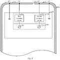
Fig. 2 is a first structural schematic view of an antenna assembly of the electronic device according to an embodiment of the present disclosure. -
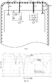
Fig. 3 is a second structural schematic view of the antenna assembly of the electronic device according to an embodiment of the present disclosure. -
Fig. 4a is a simulation schematic view of a S11 parameter of the antenna assembly according to an embodiment of the present disclosure. -
Fig. 4b is a simulation schematic view of efficiency of the antenna assembly according to an embodiment of the present disclosure. -
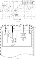
Fig. 5 is a third structural schematic view of the antenna assembly of the electronic device according to an embodiment of the present disclosure. -
Fig. 6a is a simulation schematic diagram of a S11 parameter of the antenna assembly according to another embodiment of the present disclosure. -
Fig. 6b is a simulation schematic diagram of efficiency of the antenna assembly according to another embodiment of the present disclosure. -
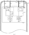
Fig. 7 is a fourth structural schematic view of the antenna assembly of the electronic device according to an embodiment of the present disclosure. -
Fig. 8 is a fifth structural schematic view of the antenna assembly of the electronic device according to an embodiment of the present disclosure. -
Fig. 9 is a sixth structural schematic view of the antenna assembly of the electronic device according to an embodiment of the present disclosure. - In order to make purposes, technical solutions, and advantages of the present disclosure more clear and more understandable, the present disclosure will be further described in detail in the following with reference to the accompanying drawings and embodiments. It should be understood that specific embodiments described herein are only configured to explain the present disclosure, but not to limit the present disclosure.
- It can be understood that terms such as "first", "second, etc., used in the present disclosure may be configured to describe various elements herein. The various elements are not limited to the terms. The terms are simply configured to distinguish a first element from another element, and not intended to indicate or imply relative importance or significance or to imply the number of indicated technical features. Thus, the feature defined with "first", "second", or the like may include one or more of such a feature. In the description of the present disclosure, it should be noted that "a plurality of' or "multiple" means two or more, unless specified otherwise.
- It should be noted that a description of an element being "attached to" another element may indicate that the element is directly on the another element or that an intervening element may exist. When an element is considered to be "connected to" another element, the element may be directly connected to the another element, or an intervening element may exist simultaneously.
- An antenna assembly according to an embodiment of the present disclosure is applied to an electronic device. In an embodiment, the electronic device may include the cellphone, a tablet computer, a notebook computer, a palmtop computer, a Mobile Internet Device (MID), a wearable device (such as a smart watch, a smart bracelet, a pedometer, etc.) or other communication modules capable of arranging an array-antenna assembly.
- As shown in
Fig. 1 , in some embodiments of the present disclosure, theelectronic device 10 may include aconductive frame 110, a rear cover, adisplay screen assembly 120, asubstrate 130 and a radio frequency circuit. Thedisplay screen assembly 120 is fixed on a housing assembly. The housing assembly includes theconductive frame 110 and the rear cover. An external structure of theelectronic device 10 may include thedisplay screen assembly 120 and the housing assembly. Thedisplay screen assembly 120 may be configured to display pictures or characters, and provide an operating interface for a user. - The rear cover is configured to define an outer contour of the
electronic device 10. The rear cover may be integrally formed. During a process of forming the rear cover, a structure such as a rear camera hole, a fingerprint-identifying module, a mounting hole of the antenna assembly or the like, may be defined or arranged on the rear cover. The rear cover may be a non-metal rear cover. For example, the rear cover may be a plastic rear cover, a ceramic rear cover, a 3D glass rear cover or the like. - In some embodiments, the
conductive frame 110 may be a frame structure defining a through hole. A material of theconductive frame 110 may include a metal frame such as an aluminum alloy metal frame, a magnesium alloy metal frame or the like. - In some embodiments, the
conductive frame 110 may be a rectangular frame with rounded corners. Theconductive frame 110 may include a first frame and a third frame opposite to the first frame. Theconductive frame 110 may include a second frame and a fourth frame opposite to the second frame. The second frame is connected to the first frame and the third frame. The first frame may be regarded as a top frame of theelectronic device 10. The third frame may be regarded as a bottom frame of theelectronic device 10. The second frame and the fourth frame may be regarded as side frames of theelectronic device 10. - The antenna assembly may be partially or wholly formed of a portion of the
conductive frame 110 of theelectronic device 10. In some embodiments, a radiator of the antenna assembly may be partially integrated on at least one of the top frame, the bottom frame, a first side frame, and a second side frame of theelectronic device 10. - The
substrate 130 may be accommodated in an accommodating space defined by theconductive frame 110 and the rear cover. Thesubstrate 130 may be a printed circuit board (PCB) or a flexible printed circuit (FPC). A part of a radio frequency circuit for processing radio frequency signals may be integrated on thesubstrate 130. A controller capable of controlling operations of theelectronic device 10 may also be integrated on thesubstrate 130. The radio frequency circuit may include but is not limited to the antenna assembly, at least one amplifier, a transceiver, a coupler, a low noise amplifier (LNA), a duplexer or the like. In addition, the radio frequency circuit may also communicate with a network and other devices by means of a wireless communication. The wireless communication mentioned above may adopt any communication standard or protocol that includes but is limited to a global system of mobile communication (GSM), a general packet radio service (GPRS), a code division multiple access (CDMA), a wideband code division multiple access (WCDMA), a long term evolution (LTE), email, a short messaging service (SMS), etc. - As shown in
Fig. 2 , an antenna assembly is provided in some embodiments of the present disclosure. The antenna assembly include theconductive frame 110, aresonance module 210 and asignal source module 220. - At least one
slot 111 may be defined in theconductive frame 110. Theconductive frame 110 may be divided by the at least oneslot 111 at least into a firstconductive branch 113 and a secondconductive branch 115 separate from each other. - In an embodiment, the
slot 111 is a part of the antenna assembly, and may be understood as a slit. Theconductive frame 110 may be divided into at least two independent conductive branches by the slit. For example, oneslot 111 may be configured to divide theconductive frame 110 into the firstconductive branch 113 the secondconductive branch 115 separating from each other. When the number of the at least oneslot 111 is N, theconductive frame 110 may be divided into N+1 independent conductive branches. - In some embodiments, the
slot 111 may be filled with air, plastic and/or other dielectrics. - In some embodiments, a shape of the
slot 111 may be substantially straight. Alternatively, theslot 111 may have one or more curved shapes. - It should be noted that, the
slot 111 may be defined in any position of theconductive frame 110. In some embodiments of the present disclosure, the shape, a size, the number of the at least oneslot 111, and the position where theslot 111 is defined in theconductive frame 110 are not further limited. - Each conductive branch may be provided with a corresponding feed point. A first feed point S1 may be arranged on the first
conductive branch 113. A second feed point S2 may be arranged on the secondconductive branch 115. - The
resonant module 210 may include a firstresonant circuit 211 and a secondresonant circuit 213. - The
signal source module 220 may include afirst signal source 221 and asecond signal source 223. Thefirst signal source 221 may be configured to output a first current signal. Thesecond signal source 223 may be configured to output a second current signal. - The first
resonant circuit 211 may filter and tune the received first current signal, such that a plurality of resonant frequencies may be excited on the firstconductive branch 113 after a tuned first current signal is fed to the firstconductive branch 113. In this way, a first radiator on the firstconductive branch 113 may be enabled to radiate a first radio frequency signal with a plurality of operating frequency bands. - Further, the first
resonant circuit 211 may further configured to filter out radio frequency signals other than a frequency corresponding to the first current signal, such that the first current signal is in a state of conduction or in a ON state when flowing through the firstresonant circuit 211. - The second
resonant circuit 213 may filter and tune the received second current signal, such that at least one resonant frequency may be excited on the secondconductive branch 115 after a tuned second current signal is fed to the secondconductive branch 115. In this way, a second radiator on the secondconductive branch 115 may be enabled to radiate a second radio frequency signal with at least an operating frequency band. - Further, the second
resonant circuit 213 may further be configured to filter out radio frequency signals other than a frequency corresponding to the second current signal, such that the second current signal is in a state of conduction or in a ON state when flowing through the secondresonant circuit 213. - According to the antenna assembly described above, the
conductive frame 110 may be divided into the firstconductive branch 113 and the secondconductive branch 115 through defining theslot 111 in theconductive frame 110. The plurality of resonant frequencies may be excited on the firstconductive branch 113 through the firstresonant circuit 211, such that the first radiator of the firstconductive branch 113 may radiate the first radio frequency signal with a plurality of operating frequency bands simultaneously. The at least one resonant frequency may be excited on the secondconductive branch 115 through the secondresonant circuit 213, such that the second radiator of the secondconductive branch 115 may radiate the second radio frequency signal with at least one operating frequency band simultaneously. In this way, a design of the antenna having dual conductive branches sharing a common aperture may be achieved, such that the first radio frequency signal and the second radio frequency signal may share a common slot, and space-utilizing rates of theslot 111 and theconductive frame 110 of theelectronic device 10 may be increased. In addition, there is no need to design an antenna radiator arranged separately, thereby reducing a thickness of the cellphone. - In some embodiments, the first radiator and the second radiator may be integrated on the first frame or the third frame of the
electronic device 10, such that a utilizing rate of the top frame or a utilizing rate of the bottom frame may be increased, and a pressure of integrating the antenna assembly on the side frames may be reduced. In this way, the profile heights of the side frames may be reduced, and the profile heights of the side frames may be reduced to values being less than 1 mm. The profile heights of the side frames may be regarded as metal widths of the metal frame in a thickness direction of theelectronic device 10. A profile height of theconductive frame 110 is one of the main factors affecting a radiating efficiency of theconductive frame 110. Under a background that a curvature of a side surface of a curved screen is getting larger and larger, even if antenna clearances of the side frames configured for integrating the antennas are greatly reduced, the antenna assembly may be integrated on the top frame or the bottom frame, without affecting flexibility and performances of the antenna assembly. - In some embodiments, the operating frequency bands of the first radio frequency signal may include two operating frequency bands of an LTE signal, an operating frequency band of a satellite positioning signal and a first operating frequency band of a Wi-Fi signal.
- The LTE signal may be divided into a Low band (LB) signal, a Middle band (MB) signal and a High band (HB) signal. In some embodiments of the present disclosure, the two operating frequency bands of the LTE signal may include the MB signal and the HB signal. A frequency range of the MB signal may be in the range of 1710MHz to 2170MHz A frequency range of the HB signal may be in the range of 2300MHz to 2690MHz
- The satellite positioning signal may include at least one of a Global Positioning System (GPS) signal with a frequency range of 1.2GHz-1.6GHz, a BeiDou Navigation Satellite System (BDS) signal, and a Global Navigation Satellite System (GLONASS) signal. In some embodiments of the present disclosure, an operating frequency band of the satellite positioning signal may include an L1 frequency band.
- An operating frequency band of the Wi-Fi signal may include 2400MHz-5000MHz. In some embodiments of the present disclosure, the first operating frequency band of the Wi-Fi signal may be a 2.4G frequency band.
- In some embodiments, the operating frequency band of the second radio frequency signal may include: two operating frequency bands of a 5G signal; and a second operating frequency band of the Wi-Fi signal.
- Specifically, the operating frequency bands of the 5G signal may at least include an N78 frequency band and an N79 frequency band. The frequency range of the N78 frequency band may be in the range of 3.3GHz ~ 3.6GHz. The frequency range of the N79 frequency band may be in the range of 4.8GHz ~ 5GHz. The second operating frequency band of the Wi-Fi signal may be a Wi-
Fi 5G signal frequency band. In some embodiments of the present disclosure, under an action of the firstresonant circuit 211, the first current signal may be fed into the firstconductive branch 113 via the first feed point S1, and excite, in the firstconductive branch 113, resonant frequencies resonating in an MHB frequency band of the LTE, an L1 frequency band of the GPS signal and a 2.4G frequency band of the WIFI signal. In this way, at least two resonant frequencies in the MHB frequency band of the LTE, the L1 frequency band of the GPS signal and the 2.4G frequency band of the Wi-Fi signal are generated in the firstconductive branch 113. Therefore, the first radiator of the firstconductive branch 113 may realize the first radio frequency signal that radiates the MHB frequency band of the LTE, the L1 frequency band of the GPS signal and the 2.4G frequency band of the Wi-Fi signal simultaneously. Under an action of the secondresonant circuit 213, the second current signal may be fed into the secondconductive branch 115 via the second feed point S2, and excite, in the secondconductive branch 115, the second current signal resonating in the N78 frequency band and the N79 frequency band of the 5G signal and in the 5G frequency band of the Wi-Fi signal. In this way, the second radiator of the secondconductive branch 115 may realize the second radio frequency signal that radiates the at least one frequency band of the N78 frequency band and the N79 frequency band of the 5G signal and the 5G frequency band of the Wi-Fi signal simultaneously. - As shown in
Fig. 3 , in some embodiments, the firstconductive branch 113 may further be provided with a first ground-returning point G1. The first feed point S1 may be arranged close to theslot 111. The first ground-returning point G1 may be arranged away from theslot 111. The firstconductive branch 113 between theslot 111 and the first ground-returning point G1 may form the first radiator. - The
first signal source 221 and the firstresonant circuit 211 may both be arranged on thesubstrate 130. The firstresonant circuit 211 may be coupled to the firstconductive branch 113 via a firstelectrical feeding part 251. The firstelectrical feeding part 251 may be a conductive elastic sheet or a screw. A coupling point between the conductive elastic sheet or the screw and the firstconductive branch 113 may be the first feed point S1. The first feed point S1 may be connected to the firstresonant circuit 211 through the firstelectrical feeding part 251. The first current signal output from thefirst signal source 221 may pass through the firstresonant circuit 211, and then be fed into the firstconductive branch 113 via the first feed point S1 by feeding of the elastic sheet or the screw. In this way, a current signal for generating a plurality of resonant frequencies may be excited in the first radiator. - In some embodiments, the first ground-returning point G1 may be connected to a ground layer of the
substrate 130 through thefirst connection portion 252, such that a connectivity of the first ground-returning point G1 with the ground may be realized. Thefirst connection portion 252 may be a conductor or a flexible circuit board. The conductor may be an elastic sheet or a screw or the like. Thefirst connection portion 252 may also be a connection arm. The connection arm may be made from the same material as the firstconductive branch 113. For example, thefirst connection portion 252 and the firstconductive branch 113 may be integrally formed, to simplify the structure of the antenna assembly. - In some embodiments, the first
resonant circuit 211 may include a low-pass filter circuit. The firstconductive branch 113 may be configured to generate two resonant frequencies under the resonant action of the firstresonant circuit 211. - It should be appreciated that, the low-pass filter circuit is configured as: when the first current signal passes, the first
resonant circuit 211 is in an ON or conductive state; and a non-first current signal with a frequency higher than that corresponding to the first current signal is blocked and could not pass the firstresonant circuit 211. - In some embodiments, the low-pass filter circuit may include a first capacitor C1 and a first inductor L1. A first end of the first inductor L1 may be connected to a first end of the first capacitor C1 and the first feed point S1. A second end of the first inductor L1 may be connected to the
first signal source 221. A second end of the first capacitor C1 may be grounded. - It should be noted that, the low-pass filter circuit may be formed of other components, and is not limited to the embodiments illustrated in the present disclosure.
- As shown in
Figs. 4a and4b , by arranging the firstresonant circuit 211 in the antenna assembly, dual resonant frequencies may be generated in the firstconductive branch 113. One resonant frequency of the dual resonant frequencies is the L1 frequency band of the GPS signal, the other resonant frequency of the dual resonant frequencies is the 2.4G frequency band of the Wi-Fi signal. When the first radiator of the firstconductive branch 113 radiates the first radio frequency signal, the total efficiency and the radiation efficiency of the first radiator radiating each operating frequency band of the first radio frequency signal meet the communication requirements. - As shown in
Fig. 5 , in some embodiments, the firstresonant circuit 211 may include a band-stop and band-pass circuit. Three resonant frequencies may be generated in the firstconductive branch 113 under the resonance adjustment of the firstresonant circuit 211. - In some embodiments, the band-stop and band-pass circuit may include a second capacitor C2, a third capacitor C3, a second inductor L2 and a third inductor L3. A first end of the second inductor L2 and a first end of the second capacitor C2 are both grounded. A second end of the second inductor L2 may be connected to the first feed point S1, a second end of the second capacitor C2, a first end of the third capacitor C3 and a first end of the third inductor L3. A second end of the third capacitor C3 and a second end of the third inductor L3 may both be connected to the
first signal source 221. - It should be appreciated that, the band-stop and band-pass circuit is configured as: when the first current signal passes, the first
resonant circuit 211 is in an ON state or in a conductive state; and a non-first current signal with a frequency higher or lower than that corresponding to the first current signal is blocked and could not pass the firstresonant circuit 211. - It should be noted that, the band-stop and band-pass circuit may be formed of other components, and is not limited to the embodiments illustrated in the present disclosure.
- As shown in
Figs. 6a and 6b , by arranging the firstresonant circuit 211 in the antenna assembly, three resonant frequencies may be generated in the firstconductive branch 113. A first one of the three resonant frequencies is the L1 frequency band of the GPS signal, a second one of the three resonant frequencies is the medium-high frequency signal frequency band of the LTE signal, and a third one of the three resonant frequencies is the 2.4G frequency band of the Wi-Fi signal. When the first radiator of the firstconductive branch 113 radiates the first radio frequency signal, the system efficiency and the radiation efficiency of each operating frequency band of each first radio frequency signal meet the communication requirements. - In some embodiments, a plurality of resonant frequencies are generated in the second
conductive branch 115 under the resonance adjustment of the secondresonant circuit 213, such that the second radiator of the secondconductive branch 115 may radiate the second radio frequency signal with a plurality of operating frequency bands. - As shown in
Figs. 7 and8 , in some embodiments, the secondresonant circuit 213 is a high-pass filter circuit. It should be appreciated that, the high-pass filter circuit is configured as: when the second current signal passes, the secondresonant circuit 213 is in an ON state or in a conductive state; and a non-second current signal with a frequency lower than that corresponding to the second current signal is blocked and could not pass the secondresonant circuit 213. - Specifically, the second
resonant circuit 213 may include a fourth capacitor C4 and a fourth inductor L4. A first end of the fourth capacitor C4 may be connected to the second feed point S2 and a first end of the fourth inductor L4. The other end of the fourth capacitor C4 is connected to thesecond signal source 223. A second end of the fourth inductor L4 is grounded. - It should be noted that, the high-pass filter circuit may be formed of other components, and is not limited to the embodiments illustrated in the present disclosure.
- In some embodiments of the present disclosure, as shown in
Figs. 4a-4b andFigs. 6a-6b , under an action of the secondresonant circuit 213, the second current signal may be fed into the secondconductive branch 115 via the second feed point S2, and excite, in the secondconductive branch 115, resonant frequencies resonating in the N78 frequency band and the N79 frequency band of the 5G signal and in the 5G frequency band of the Wi-Fi signal. In this way, the second radiator of the secondconductive branch 115 may realize the second radio frequency signal that radiates the N78 frequency band and the N79 frequency band of the 5G signal and the 5G frequency band of the Wi-Fi signal. - In some embodiments, a second ground-returning point G2 is provided on the second
conductive branch 115. The second feed point S2 is arranged close to theslot 111. The second ground-returning point G2 is arranged away from theslot 111. The secondconductive branch 115 between theslot 111 and the second ground-returning point G2 may form the second radiator. - The
second signal source 223 and the secondresonant circuit 213 may both be arranged on thesubstrate 130. The secondresonant circuit 213 may be coupled to the secondconductive branch 115 via a secondelectrical feeding part 253. A coupling point between the secondelectrical feeding part 253 and the secondconductive branch 115 may be configured as the second feed point S2. The secondelectrical feeding part 253 may be a conductive elastic sheet or a screw. The second feed point S2 may be connected to the secondresonant circuit 213 through the conductive elastic sheet or the screw. The second current signal output from thesecond signal source 223 may pass through the secondresonant circuit 213, and then be fed into the secondconductive branch 115 via the second feed point S2 by feeding of the elastic sheet or the screw. In this way, a plurality of resonant frequencies may be excited in the secondconductive branch 115, thereby generating radiation. That is, the second radiator of the secondconductive branch 115 may be caused to radiate the second radio frequency signal with a plurality of operating frequency bands. - In some embodiments, the second ground-returning point G2 may be connected to the ground layer of the
substrate 130 through thesecond connection portion 254, such that a connectivity of the second ground-returning point G2 with the ground may be realized. Thesecond connection portion 254 may be a conductor or a flexible circuit board. The conductor may be an elastic sheet or a screw or the like. Thesecond connection portion 254 may also be a connection arm. The connection arm may be made from the same material as the secondconductive branch 115. For example, thesecond connection portion 254 and the secondconductive branch 115 may be integrally formed, to simplify the structure of the antenna assembly. - The operating frequency bands of the first radio frequency signal may be varied by changing a length dimension of the first radiator. The operating frequency bands of the second radio frequency signal may be varied by changing a length dimension of the second radiator. The longer the radiator is, the lower is the frequency band that can be covered by the radiator. In the present disclosure, the length dimension of the first radiator may be greater than that of the second radiator. The length dimension may be appreciated as a dimension in an extending direction of the conductive frame on the electronic device.
- It should be noted that, frequencies within a range of 7-13% of a resonant frequency may be regarded as an operating bandwidth of the antenna. For example, when the resonant frequency of the antenna is 1800MHz, and the operating bandwidth is 10% of the resonant frequency, then an operating frequency band of the antenna may be in the range of 1620MHz-1980MHz.
- As shown in
Fig. 9 , in some embodiments, afirst matching circuit 241 configured for adjusting the first current signal may be arranged between the firstconductive branch 113 and thefirst signal source 221. Thefirst matching circuit 241 may be configured for adjusting an input impedance of the first radiator, so as to increase a transmitting performance of the first radiator. - A
second matching circuit 243 configured for adjusting the radio frequency signal of the second current signal may further be arranged between the secondconductive branch 115 and thesignal source 223. Thesecond matching circuit 243 may be configured for adjusting an input impedance of the second radiator, so as to increase a transmitting performance of the second radiator. - Specifically, each of the
first matching circuit 241 and thesecond matching circuit 243 may include a combination of a capacitor rand/or an inductor or the like. In some embodiments of the present disclosure, specific composition forms of thefirst matching circuit 241 and thesecond matching circuit 243 are not further limited. - It should be noted that, the first feed point S1 may be arranged close to the
slot 111, the second feed point S2 may also be arranged close to theslot 111. It should be understood that, a specific position of the first feed point S1 may be associated with thefirst matching circuit 241. That is, the specific position of the first feed point S1 may be arranged based on thefirst matching circuit 241. Accordingly, a specific position of the second feed point S2 may be associated with thesecond matching circuit 243. That is, the specific position of the second feed point S2 may be arranged based on thesecond matching circuit 243. - In some embodiments, the
conductive frame 110 may be divided into the firstconductive branch 113 and the secondconductive branch 115 through defining theslot 111 in theconductive frame 110. The firstresonant circuit 211 may tune the first current signal fed to a middle position of the firstconductive branch 113, such that a plurality of resonant frequencies resonating in the MHB frequency band of the LTE signal, the L1 frequency band of the GPS signal and the 2.4G frequency band of the Wi-Fi signal may be excited in the firstconductive branch 113. The secondresonant circuit 213 may tune the second current signal fed to a position of the secondconductive branch 115 close to theslot 111, such that a plurality of resonant frequencies resonating in the N78 frequency band and the N79 frequency band of the 5G signal and in the 5G frequency band of the Wi-Fi signal may be excited in the secondconductive branch 115. In this way, the design of the antenna having dual conductive branches sharing the common aperture may be achieved. The GPS signal, the MHB signal, the N78 signal, the N79 signal and the Wi-Fi signal may share the common slot, such that space-utilizing rates of the slot and the whole device may be increased. - In some embodiments, the number of
slots 111 defined in theconductive frame 110 may be multiple. In some embodiments, two slots are taken as an example for description. The two slots may include a first slot and a second slot. Theconductive frame 110 may be divided into the firstconductive branches 113, the secondconductive branches 115 and a third conductive branch separating from each other by the first slot and the second slot. Each of these conductive branches may be correspondingly provided with a feed point and a ground-returning point. The first radiator for radiating the first radio frequency signal may be integrated in the firstconductive branch 113. The second radiator for radiating the second radio frequency signal may be integrated in the secondconductive branch 115. A third radiator for radiating a third radio frequency signal may be integrated in the third conductive branch. The third radio frequency signal may be a 2G signal, a 3G signal, a Bluetooth signal, etc. - Further, each feed point may be connected to a filter circuit through the conductive elastic sheet or the screw, and connected to a corresponding signal source through the resonant circuit. Each signal source may feed the current signal to a corresponding conductive branch through the resonant circuit, the conductive elastic sheet or the screw and the feed point, such that a one-quarter current or currents in other modes may be excited on a conductive branch (the radiator) between the slot and the ground-returning point. In this way, a radiation may be generated, and different radio signals may be radiated.
- By analogy, when N (N>2)
slots 111 are defined in theconductive frame 110, theconductive frame 110 may be divided into N+1 independent conductive branches. Correspondingly, N+1 resonant circuits and N+1 signal sources may also be arranged. N+1 radiators may each be integrated in one of the N+1 independent conductive branches correspondingly, and configured to radiate N+1 radio frequency signals. Each of these radio frequency signals may have different operating frequency bands. - An
electronic device 10 is further provided in some embodiments of the present disclosure. Theelectronic device 10 may include thesubstrate 130 and the antenna assembly as described in any of the foregoing embodiments. Thesubstrate 130 may be accommodated in a cavity enclosed by theconductive frame 110. Theresonant module 210 and thesignal source module 220 may be arranged on thesubstrate 130. - When the antenna assembly is applied in the
electronic device 10, the firstconductive branch 113 and the secondconductive branch 115 may share thesame slot 111, such that the firstconductive branch 113 may radiate the first radio frequency signal and the secondconductive branch 115 may radiate the second radio frequency signal at the same time. In this way, the space-utilizing rates of theslot 111 and theconductive frame 110 of theelectronic device 10 may be increased. In addition, there is no need to design an antenna radiator separately, thereby reducing the thickness of the cellphone. - As an example, due to the design of the common-aperture-shared antenna, the GPS signal, the MHB signal, the N78 signal, the N79 signal and the Wi-Fi signal may share the same slot, such that the first radiator and the second radiator may be integrated on the first frame or the third frame of the
electronic device 10. In this way, the utilizing rate of the top frame or the utilizing rate of the bottom frame may be increased, and the pressure of integrating the antenna assembly on the side frames may be reduced. Therefore, the profile heights of the side frames may be reduced, and the profile heights of the side frames may be reduced to values less than 1mm. The profile heights of the side frames may be regarded as the metal widths of themetal frame 110 in the thickness direction of theelectronic device 10. The profile height of theconductive frame 110 is one of the main factors affecting the radiating efficiency of theconductive frame 110. Under the background that the curvature of the side surface of the curved screen is getting larger and larger, the profile heights of the side frames may be limited, resulting in the antenna clearances being greatly reduced. By adopting the design of the common-aperture-shared antenna according to the embodiments of the present disclosure, the antenna assembly may be integrated on the top frame or the bottom frame, so as to ensure that the antenna has an enough clearance. In addition, by arranging the first resonant circuit in the antenna assembly, the first current signal for generating a plurality of resonant frequencies may be excited in the first conductive branch, such that the first radiator of the first conductive branch may simultaneously radiate the first radio frequency signal including a plurality of operating frequency bands. In this way, a design requirement of multiple frequency bands and multiple antennas may be satisfied with the top frame or the bottom frame having a limited radiator length. - Any reference to a memory, a storage, a database or other media made in the embodiments of the present disclosure may include a non-volatile memory and/or a volatile memory. Suitable non-volatile memory may include a read only memory (ROM), a programmable ROM (PROM), an electrically programmable ROM (EPROM) an electrically erasable programmable ROM (EEPROM), or a flash memory. The volatile memory may include a random access memory (RAM), which may be configured as an external cache memory. As illustration but not limitation, RAM nay be available in various forms, such as a static RAM (SRAM), a dynamic RAM (DRAM), a synchronous DRAM (SDRAM), a double data rate SDRAM (DDR SDRAM), an enhanced SDRAM (ESDRAM), a synchronous Link (Synchlink) DRAM (SLDRAM), a Memory Bus (Rambus) Direct RAM (RDRAM), a Direct Rambus Dynamic RAM (DRDRAM), and a Rambus Dynamic RAM (RDRAM).
- Each technical feature in the above embodiments may be combined arbitrarily. For a concise description, all possible combinations of various technical features in the above embodiments are not described. Each combination of these technical features which has no contradiction should be regarded within a scope recited by the specification.
- Only some implementations of the present disclosure are described in the above embodiments, descriptions of which are relatively specific and detailed but should not be construed as limitations to a patent scope of the present disclosure. It should be noted that those skilled in the art may make some modifications and improvements without departing from a concept of the present disclosure. All of the modifications and improvements belong to a protection scope of the present disclosure. Therefore, the protection scope of the present disclosure shall be subject to the appended claims.
Claims (20)
the first resonant circuit comprises a low-pass filter circuit, wherein two resonant frequencies are generated in the first conductive branch under resonance adjustment of the first resonant circuit.
a plurality of resonant frequencies are generated in the second conductive branch under resonance adjustment of the second resonant circuit.
the second resonant circuit is a high-pass filter circuit.
resonant frequencies resonating in an N78 frequency band and an N79 frequency band of a 5G signal and in a 5G frequency band of a Wi-Fi signal are excited in the second conductive branch under resonance adjustment of the second resonant circuit.
each of the first matching circuit and the second matching circuit comprises a capacitor and/or an inductor.
a length dimension of the first conductive branch is greater than that of the second conductive branch.
the conductive frame comprises a first frame and a third frame opposite to the first frame, a second frame and a fourth frame opposite to the second frame, the second frame is connected to the first frame and the third frame, the first conductive branch and the second conductive branch are integrated in the first frame or the third frame of the electronic device.
Applications Claiming Priority (3)
| Application Number | Priority Date | Filing Date | Title |
|---|---|---|---|
| CN202020306607.3U CN212136680U (en) | 2020-03-12 | 2020-03-12 | Antenna Components and Electronics |
| CN202010169499.4A CN113394547A (en) | 2020-03-12 | 2020-03-12 | Antenna assembly and electronic equipment |
| PCT/CN2021/073689 WO2021179813A1 (en) | 2020-03-12 | 2021-01-26 | Antenna assembly and electronic device |
Publications (2)
| Publication Number | Publication Date |
|---|---|
| EP4106103A1 true EP4106103A1 (en) | 2022-12-21 |
| EP4106103A4 EP4106103A4 (en) | 2023-09-13 |
Family
ID=77671189
Family Applications (1)
| Application Number | Title | Priority Date | Filing Date |
|---|---|---|---|
| EP21768360.6A Withdrawn EP4106103A4 (en) | 2020-03-12 | 2021-01-26 | ANTENNA ARRANGEMENT AND ELECTRONIC DEVICE |
Country Status (3)
| Country | Link |
|---|---|
| US (1) | US20230006336A1 (en) |
| EP (1) | EP4106103A4 (en) |
| WO (1) | WO2021179813A1 (en) |
Cited By (1)
| Publication number | Priority date | Publication date | Assignee | Title |
|---|---|---|---|---|
| EP4224631A4 (en) * | 2020-09-30 | 2024-04-10 | Guangdong Oppo Mobile Telecommunications Corp., Ltd. | ANTENNA AND ELECTRONIC DEVICE ASSEMBLY |
Families Citing this family (3)
| Publication number | Priority date | Publication date | Assignee | Title |
|---|---|---|---|---|
| EP4113741A4 (en) * | 2020-03-12 | 2023-08-02 | Guangdong Oppo Mobile Telecommunications Corp., Ltd. | ANTENNA ARRANGEMENT AND ELECTRONIC DEVICE |
| CN115332792B (en) * | 2021-05-11 | 2025-05-13 | Oppo广东移动通信有限公司 | Antenna structure and electronic equipment |
| CN114221127B (en) * | 2021-11-30 | 2022-11-01 | 荣耀终端有限公司 | Self-decoupling broadband antenna system and terminal equipment |
Family Cites Families (12)
| Publication number | Priority date | Publication date | Assignee | Title |
|---|---|---|---|---|
| CN104993241A (en) * | 2015-05-21 | 2015-10-21 | 深圳市万普拉斯科技有限公司 | Mobile terminal and antenna device thereof |
| CN104852122A (en) * | 2015-06-09 | 2015-08-19 | 联想(北京)有限公司 | Electronic equipment and antenna device |
| US10056695B2 (en) * | 2015-07-28 | 2018-08-21 | Apple Inc. | Electronic device antenna with switchable return paths |
| CN109390693B (en) * | 2017-08-05 | 2021-12-07 | 深圳富泰宏精密工业有限公司 | Antenna structure and wireless communication device with same |
| TWI678028B (en) * | 2017-12-12 | 2019-11-21 | 群邁通訊股份有限公司 | Antenna structure and wireless communication device with same |
| CN207800915U (en) * | 2017-12-29 | 2018-08-31 | 瑞声精密制造科技(常州)有限公司 | A kind of antenna system and mobile terminal |
| CN110137671B (en) * | 2018-02-09 | 2020-11-24 | 深圳富泰宏精密工业有限公司 | Antenna structure and wireless communication device having the same |
| CN108470977B (en) * | 2018-03-28 | 2020-07-03 | Oppo广东移动通信有限公司 | Antenna assemblies, antenna devices and electronic equipment |
| CN108832272B (en) * | 2018-05-29 | 2020-08-21 | 北京小米移动软件有限公司 | Electronic equipment and its antenna structure |
| CN109687115A (en) * | 2019-01-28 | 2019-04-26 | 广州三星通信技术研究有限公司 | GPS antenna structure and electric terminal for electric terminal |
| CN212136686U (en) * | 2020-03-12 | 2020-12-11 | Oppo广东移动通信有限公司 | Antenna Components and Electronics |
| CN212136680U (en) * | 2020-03-12 | 2020-12-11 | Oppo广东移动通信有限公司 | Antenna Components and Electronics |
-
2021
- 2021-01-26 WO PCT/CN2021/073689 patent/WO2021179813A1/en not_active Ceased
- 2021-01-26 EP EP21768360.6A patent/EP4106103A4/en not_active Withdrawn
-
2022
- 2022-09-08 US US17/941,001 patent/US20230006336A1/en not_active Abandoned
Cited By (1)
| Publication number | Priority date | Publication date | Assignee | Title |
|---|---|---|---|---|
| EP4224631A4 (en) * | 2020-09-30 | 2024-04-10 | Guangdong Oppo Mobile Telecommunications Corp., Ltd. | ANTENNA AND ELECTRONIC DEVICE ASSEMBLY |
Also Published As
| Publication number | Publication date |
|---|---|
| US20230006336A1 (en) | 2023-01-05 |
| EP4106103A4 (en) | 2023-09-13 |
| WO2021179813A1 (en) | 2021-09-16 |
Similar Documents
| Publication | Publication Date | Title |
|---|---|---|
| CN211350951U (en) | Antenna Components and Electronics | |
| CN212136680U (en) | Antenna Components and Electronics | |
| CN211350950U (en) | Antenna assembly and electronic equipment | |
| US20230006336A1 (en) | Antenna Assembly and Electronic Device | |
| CN212136686U (en) | Antenna Components and Electronics | |
| US20230006345A1 (en) | Antenna Assembly and Electronic Device | |
| CN113394547A (en) | Antenna assembly and electronic equipment | |
| US12394884B2 (en) | Antenna assembly and electronic device | |
| CN104795623B (en) | Mobile device and manufacturing method thereof | |
| US9531058B2 (en) | Loosely-coupled radio antenna apparatus and methods | |
| EP2959541B1 (en) | Multiple antenna system | |
| CN112928456A (en) | Antenna assembly and electronic equipment | |
| EP2448062B1 (en) | Communication device and antenna thereof | |
| CN113394545B (en) | Antenna Assemblies and Electronic Devices | |
| US10490902B2 (en) | Mobile device | |
| US10797379B1 (en) | Antenna structure | |
| US20230006335A1 (en) | Antenna assembly and electronic device | |
| CN111697317B (en) | Mobile device | |
| CN113394546A (en) | Antenna assembly and electronic equipment | |
| CN211350948U (en) | Antenna Components and Electronics | |
| TW201834312A (en) | Mobile device | |
| CN113948863A (en) | Signal feed-in assembly, antenna module and electronic equipment | |
| CN113394550B (en) | Antenna Assemblies and Electronic Devices | |
| CN116315658A (en) | Antenna components and electronics | |
| CN107994316B (en) | Antenna system and communication terminal |
Legal Events
| Date | Code | Title | Description |
|---|---|---|---|
| STAA | Information on the status of an ep patent application or granted ep patent |
Free format text: STATUS: THE INTERNATIONAL PUBLICATION HAS BEEN MADE |
|
| PUAI | Public reference made under article 153(3) epc to a published international application that has entered the european phase |
Free format text: ORIGINAL CODE: 0009012 |
|
| STAA | Information on the status of an ep patent application or granted ep patent |
Free format text: STATUS: REQUEST FOR EXAMINATION WAS MADE |
|
| 17P | Request for examination filed |
Effective date: 20220912 |
|
| AK | Designated contracting states |
Kind code of ref document: A1 Designated state(s): AL AT BE BG CH CY CZ DE DK EE ES FI FR GB GR HR HU IE IS IT LI LT LU LV MC MK MT NL NO PL PT RO RS SE SI SK SM TR |
|
| DAV | Request for validation of the european patent (deleted) | ||
| DAX | Request for extension of the european patent (deleted) | ||
| A4 | Supplementary search report drawn up and despatched |
Effective date: 20230811 |
|
| RIC1 | Information provided on ipc code assigned before grant |
Ipc: H01Q 5/50 20150101ALI20230807BHEP Ipc: H01Q 5/35 20150101ALI20230807BHEP Ipc: H01Q 5/335 20150101ALI20230807BHEP Ipc: H01Q 1/44 20060101ALI20230807BHEP Ipc: H01Q 1/24 20060101AFI20230807BHEP |
|
| STAA | Information on the status of an ep patent application or granted ep patent |
Free format text: STATUS: THE APPLICATION HAS BEEN WITHDRAWN |
|
| 18W | Application withdrawn |
Effective date: 20231121 |