EP4106032A1 - Light-emitting device and electronic apparatus including the same - Google Patents

Light-emitting device and electronic apparatus including the same Download PDF

Info

Publication number
EP4106032A1
EP4106032A1 EP22177369.0A EP22177369A EP4106032A1 EP 4106032 A1 EP4106032 A1 EP 4106032A1 EP 22177369 A EP22177369 A EP 22177369A EP 4106032 A1 EP4106032 A1 EP 4106032A1
Authority
EP
European Patent Office
Prior art keywords
group
light
emitting device
emission layer
electrode
Prior art date
Legal status (The legal status is an assumption and is not a legal conclusion. Google has not performed a legal analysis and makes no representation as to the accuracy of the status listed.)
Pending
Application number
EP22177369.0A
Other languages
German (de)
French (fr)
Inventor
Seungyeon Kwak
Byungjoon KANG
Hyungjun Kim
Myungsun Sim
Kum Hee Lee
Sunghun Lee
Byoungki Choi
Current Assignee (The listed assignees may be inaccurate. Google has not performed a legal analysis and makes no representation or warranty as to the accuracy of the list.)
Samsung Display Co Ltd
Original Assignee
Samsung Electronics Co Ltd
Priority date (The priority date is an assumption and is not a legal conclusion. Google has not performed a legal analysis and makes no representation as to the accuracy of the date listed.)
Filing date
Publication date
Application filed by Samsung Electronics Co Ltd filed Critical Samsung Electronics Co Ltd
Publication of EP4106032A1 publication Critical patent/EP4106032A1/en
Pending legal-status Critical Current

Links

Images

Classifications

    • HELECTRICITY
    • H10SEMICONDUCTOR DEVICES; ELECTRIC SOLID-STATE DEVICES NOT OTHERWISE PROVIDED FOR
    • H10KORGANIC ELECTRIC SOLID-STATE DEVICES
    • H10K50/00Organic light-emitting devices
    • H10K50/80Constructional details
    • H10K50/85Arrangements for extracting light from the devices
    • H10K50/852Arrangements for extracting light from the devices comprising a resonant cavity structure, e.g. Bragg reflector pair
    • CCHEMISTRY; METALLURGY
    • C09DYES; PAINTS; POLISHES; NATURAL RESINS; ADHESIVES; COMPOSITIONS NOT OTHERWISE PROVIDED FOR; APPLICATIONS OF MATERIALS NOT OTHERWISE PROVIDED FOR
    • C09KMATERIALS FOR MISCELLANEOUS APPLICATIONS, NOT PROVIDED FOR ELSEWHERE
    • C09K11/00Luminescent materials, e.g. electroluminescent or chemiluminescent
    • C09K11/06Luminescent materials, e.g. electroluminescent or chemiluminescent containing organic luminescent materials
    • HELECTRICITY
    • H10SEMICONDUCTOR DEVICES; ELECTRIC SOLID-STATE DEVICES NOT OTHERWISE PROVIDED FOR
    • H10KORGANIC ELECTRIC SOLID-STATE DEVICES
    • H10K50/00Organic light-emitting devices
    • H10K50/10OLEDs or polymer light-emitting diodes [PLED]
    • H10K50/11OLEDs or polymer light-emitting diodes [PLED] characterised by the electroluminescent [EL] layers
    • HELECTRICITY
    • H10SEMICONDUCTOR DEVICES; ELECTRIC SOLID-STATE DEVICES NOT OTHERWISE PROVIDED FOR
    • H10KORGANIC ELECTRIC SOLID-STATE DEVICES
    • H10K50/00Organic light-emitting devices
    • H10K50/10OLEDs or polymer light-emitting diodes [PLED]
    • H10K50/11OLEDs or polymer light-emitting diodes [PLED] characterised by the electroluminescent [EL] layers
    • H10K50/12OLEDs or polymer light-emitting diodes [PLED] characterised by the electroluminescent [EL] layers comprising dopants
    • HELECTRICITY
    • H10SEMICONDUCTOR DEVICES; ELECTRIC SOLID-STATE DEVICES NOT OTHERWISE PROVIDED FOR
    • H10KORGANIC ELECTRIC SOLID-STATE DEVICES
    • H10K50/00Organic light-emitting devices
    • H10K50/10OLEDs or polymer light-emitting diodes [PLED]
    • H10K50/11OLEDs or polymer light-emitting diodes [PLED] characterised by the electroluminescent [EL] layers
    • H10K50/125OLEDs or polymer light-emitting diodes [PLED] characterised by the electroluminescent [EL] layers specially adapted for multicolour light emission, e.g. for emitting white light
    • HELECTRICITY
    • H10SEMICONDUCTOR DEVICES; ELECTRIC SOLID-STATE DEVICES NOT OTHERWISE PROVIDED FOR
    • H10KORGANIC ELECTRIC SOLID-STATE DEVICES
    • H10K50/00Organic light-emitting devices
    • H10K50/10OLEDs or polymer light-emitting diodes [PLED]
    • H10K50/11OLEDs or polymer light-emitting diodes [PLED] characterised by the electroluminescent [EL] layers
    • H10K50/125OLEDs or polymer light-emitting diodes [PLED] characterised by the electroluminescent [EL] layers specially adapted for multicolour light emission, e.g. for emitting white light
    • H10K50/13OLEDs or polymer light-emitting diodes [PLED] characterised by the electroluminescent [EL] layers specially adapted for multicolour light emission, e.g. for emitting white light comprising stacked EL layers within one EL unit
    • HELECTRICITY
    • H10SEMICONDUCTOR DEVICES; ELECTRIC SOLID-STATE DEVICES NOT OTHERWISE PROVIDED FOR
    • H10KORGANIC ELECTRIC SOLID-STATE DEVICES
    • H10K50/00Organic light-emitting devices
    • H10K50/10OLEDs or polymer light-emitting diodes [PLED]
    • H10K50/14Carrier transporting layers
    • H10K50/15Hole transporting layers
    • HELECTRICITY
    • H10SEMICONDUCTOR DEVICES; ELECTRIC SOLID-STATE DEVICES NOT OTHERWISE PROVIDED FOR
    • H10KORGANIC ELECTRIC SOLID-STATE DEVICES
    • H10K50/00Organic light-emitting devices
    • H10K50/10OLEDs or polymer light-emitting diodes [PLED]
    • H10K50/14Carrier transporting layers
    • H10K50/16Electron transporting layers
    • HELECTRICITY
    • H10SEMICONDUCTOR DEVICES; ELECTRIC SOLID-STATE DEVICES NOT OTHERWISE PROVIDED FOR
    • H10KORGANIC ELECTRIC SOLID-STATE DEVICES
    • H10K50/00Organic light-emitting devices
    • H10K50/80Constructional details
    • H10K50/805Electrodes
    • HELECTRICITY
    • H10SEMICONDUCTOR DEVICES; ELECTRIC SOLID-STATE DEVICES NOT OTHERWISE PROVIDED FOR
    • H10KORGANIC ELECTRIC SOLID-STATE DEVICES
    • H10K85/00Organic materials used in the body or electrodes of devices covered by this subclass
    • H10K85/30Coordination compounds
    • H10K85/341Transition metal complexes, e.g. Ru(II)polypyridine complexes
    • H10K85/342Transition metal complexes, e.g. Ru(II)polypyridine complexes comprising iridium
    • HELECTRICITY
    • H10SEMICONDUCTOR DEVICES; ELECTRIC SOLID-STATE DEVICES NOT OTHERWISE PROVIDED FOR
    • H10KORGANIC ELECTRIC SOLID-STATE DEVICES
    • H10K85/00Organic materials used in the body or electrodes of devices covered by this subclass
    • H10K85/40Organosilicon compounds, e.g. TIPS pentacene
    • CCHEMISTRY; METALLURGY
    • C09DYES; PAINTS; POLISHES; NATURAL RESINS; ADHESIVES; COMPOSITIONS NOT OTHERWISE PROVIDED FOR; APPLICATIONS OF MATERIALS NOT OTHERWISE PROVIDED FOR
    • C09KMATERIALS FOR MISCELLANEOUS APPLICATIONS, NOT PROVIDED FOR ELSEWHERE
    • C09K2211/00Chemical nature of organic luminescent or tenebrescent compounds
    • C09K2211/10Non-macromolecular compounds
    • C09K2211/1018Heterocyclic compounds
    • C09K2211/1025Heterocyclic compounds characterised by ligands
    • C09K2211/1029Heterocyclic compounds characterised by ligands containing one nitrogen atom as the heteroatom
    • CCHEMISTRY; METALLURGY
    • C09DYES; PAINTS; POLISHES; NATURAL RESINS; ADHESIVES; COMPOSITIONS NOT OTHERWISE PROVIDED FOR; APPLICATIONS OF MATERIALS NOT OTHERWISE PROVIDED FOR
    • C09KMATERIALS FOR MISCELLANEOUS APPLICATIONS, NOT PROVIDED FOR ELSEWHERE
    • C09K2211/00Chemical nature of organic luminescent or tenebrescent compounds
    • C09K2211/10Non-macromolecular compounds
    • C09K2211/1018Heterocyclic compounds
    • C09K2211/1025Heterocyclic compounds characterised by ligands
    • C09K2211/1044Heterocyclic compounds characterised by ligands containing two nitrogen atoms as heteroatoms
    • C09K2211/1048Heterocyclic compounds characterised by ligands containing two nitrogen atoms as heteroatoms with oxygen
    • CCHEMISTRY; METALLURGY
    • C09DYES; PAINTS; POLISHES; NATURAL RESINS; ADHESIVES; COMPOSITIONS NOT OTHERWISE PROVIDED FOR; APPLICATIONS OF MATERIALS NOT OTHERWISE PROVIDED FOR
    • C09KMATERIALS FOR MISCELLANEOUS APPLICATIONS, NOT PROVIDED FOR ELSEWHERE
    • C09K2211/00Chemical nature of organic luminescent or tenebrescent compounds
    • C09K2211/18Metal complexes
    • C09K2211/185Metal complexes of the platinum group, i.e. Os, Ir, Pt, Ru, Rh or Pd
    • HELECTRICITY
    • H10SEMICONDUCTOR DEVICES; ELECTRIC SOLID-STATE DEVICES NOT OTHERWISE PROVIDED FOR
    • H10KORGANIC ELECTRIC SOLID-STATE DEVICES
    • H10K2101/00Properties of the organic materials covered by group H10K85/00
    • H10K2101/10Triplet emission
    • HELECTRICITY
    • H10SEMICONDUCTOR DEVICES; ELECTRIC SOLID-STATE DEVICES NOT OTHERWISE PROVIDED FOR
    • H10KORGANIC ELECTRIC SOLID-STATE DEVICES
    • H10K2101/00Properties of the organic materials covered by group H10K85/00
    • H10K2101/90Multiple hosts in the emissive layer

Definitions

  • the present disclosure relates to light-emitting devices and electronic apparatuses including the same.
  • organic light-emitting devices are self-emissive devices, which have improved characteristics in terms of viewing angles, response time, luminance, driving voltage, and response speed, and produce full-color images.
  • an organic light-emitting device may include an anode, a cathode, and an organic layer located between the anode and the cathode and including an emission layer.
  • a hole transport region may be located between the anode and the emission layer, and an electron transport region may be located between the emission layer and the cathode.
  • Holes provided from the anode may move toward the emission layer through the hole transport region, and electrons provided from the cathode may move toward the emission layer through the electron transport region.
  • the holes and the electrons recombine in the emission layer to produce excitons. These excitons transition from an excited state to a ground state to thereby generate light.
  • light-emitting devices having a novel emission layer and electronic apparatuses including the same.
  • a light-emitting device includes
  • an electronic apparatus includes the light-emitting device.
  • relative terms such as “lower” or “bottom” and “upper” or “top,” may be used herein to describe one element's relationship to another element as illustrated in the Figures. It will be understood that relative terms are intended to encompass different orientations of the device in addition to the orientation depicted in the Figures. For example, if the device in one of the figures is turned over, elements described as being on the “lower” side of other elements would then be oriented on “upper” sides of the other elements. The exemplary term “lower,” can therefore, encompasses both an orientation of “lower” and “upper,” depending on the particular orientation of the figure.
  • Exemplary embodiments are described herein with reference to cross section illustrations that are schematic illustrations of idealized embodiments. As such, variations from the shapes of the illustrations as a result, for example, of manufacturing techniques and/or tolerances, are to be expected. Thus, embodiments described herein should not be construed as limited to the particular shapes of regions as illustrated herein but are to include deviations in shapes that result, for example, from manufacturing. For example, a region illustrated or described as flat may, typically, have rough and/or nonlinear features. Moreover, sharp angles that are illustrated may be rounded. Thus, the regions illustrated in the figures are schematic in nature and their shapes are not intended to illustrate the precise shape of a region and are not intended to limit the scope of the present claims.
  • a light-emitting device may include a first electrode, a second electrode facing the first electrode, and an emission layer between the first electrode and the second electrode.
  • the first electrode may be a reflective electrode.
  • the emission layer may include i) a first emission layer, and ii) a second emission layer between the first emission layer and the second electrode.
  • the first emission layer may be in direct contact with the second emission layer.
  • the first emission layer includes a first compound capable of emitting first light having a first spectrum
  • ⁇ P(1) is an emission peak wavelength (nm) of the first spectrum
  • the second emission layer includes a second compound capable of emitting second light having a second spectrum
  • ⁇ P(2) is an emission peak wavelength (nm) of the second spectrum
  • the emission layer may emit third light having a third spectrum
  • ⁇ P(3) is an emission peak wavelength (nm) of the third spectrum.
  • ⁇ P(1) may be less than ⁇ P(2),
  • ⁇ P(1) and ⁇ P(2) may be evaluated from photoluminescence spectra measured for a first film and a second film, respectively.
  • the "first film” is a film including the first compound
  • the "second film” is a film including the second compound.
  • the first film and the second film may be manufactured using various methods such as any method known in the art, for example, a vacuum deposition method, a coating method, and heating method.
  • the first film and the second film may further include other compounds, for example, a host described in the present specification, in addition to the first compound and the second compound.
  • a method of evaluating ⁇ P(1) and ⁇ P(2) may be the same as described in Evaluation Example 1 in the present specification.
  • ⁇ P(3) is evaluated from an electroluminescence spectrum of the light-emitting device.
  • a method of evaluating ⁇ P(3) may be the same as described in Evaluation Example 3 in the present specification.
  • the third light may be extracted to the outside of the light-emitting device through the second electrode.
  • the second electrode may be a transparent electrode or a semi-transparent electrode.
  • a first region may exist between the emission layer and the first electrode of the light-emitting device.
  • the first region may be a hole transport region.
  • the first electrode may be an anode
  • the second electrode may be a cathode
  • the third light emitted from the emission layer may vibrate between the first electrode and the second electrode according to the principle of constructive interference, and may be extracted to the outside of the light-emitting device by a microcavity effect through the second electrode.
  • the microcavity effect for the third light generated from the emission layer has a close relationship with a resonance distance which is a distance between an "interface between the emission layer and the first region (e.g., hole transport region)" and an "interface between the first region (e.g., hole transport region) and the first electrode (e.g., anode)."
  • a resonance distance which is a distance between an "interface between the emission layer and the first region (e.g., hole transport region)" and an "interface between the first region (e.g., hole transport region) and the first electrode (e.g., anode).
  • the resonance distance as described above may not always be kept constant due to deviations in a manufacturing process when a large number of the light-emitting devices are manufactured. This may cause a deviation in the emission color (i.e., light extracted toward the outside of the light-emitting device among the third light) between manufactured light-emitting devices, that is, a deviation in CIE coordinates (e.g., CIEx) and a deviation in luminescence efficiency.
  • the deviation in luminescence efficiency according to the change in CIEx may be a factor impairing process stability in mass production of light-emitting devices.
  • the first emission layer including the first compound having a smaller emission peak wavelength than that of the second compound is arranged closer to the first electrode than the second emission layer including the second compound, thereby reducing a resonance distance of the first light, which is a distance between an "interface between the first emission layer and the first region (e.g., hole transport region)" and an "interface between the first region (e.g., hole transport region) and the first electrode (e.g., anode)" and strengthening the resonance of the first light, and thus, the curvature of a CIEx-luminescence efficiency curve of the light-emitting device may be improved (i.e., becoming gentle) (e.g., see FIG. 3 ).
  • the curvature of the CIEx-luminescence efficiency curve of the light-emitting device is improved, a phenomenon, in which light observed from the side of the light-emitting device (for example, a point shifted by 45° relative to the front) is blue-shifted compared to light observed from the front thereof and thus the light observed from the side of the light-emitting device has a relatively small luminescence efficiency, is substantially prevented, and the light-emitting device may have an excellent side luminance ratio (e.g., a ratio of luminance at a point shifted to the side by 45° relative to luminance at the front).
  • may be greater than 0 nm and less than or equal to about 20 nm.
  • may be greater than 0 nm and less than or equal to about 10 nm.
  • may be greater than or equal to 0 nm and less than or equal to about 15 nm.
  • may be greater than 0 nm and less than or equal to about 20 nm.
  • may be greater than 0 nm and less than or equal to about 10 nm.
  • each of ⁇ P(1), ⁇ P(2), and ⁇ P(3) may be about 500 nm to about 570 nm.
  • each of ⁇ P(1), ⁇ P(2), and ⁇ P(3) may be about 570 nm to about 650 nm.
  • ⁇ P(1) may be about 570 nm to about 630 nm
  • ⁇ P(2) may be about 620 nm to about 650 nm
  • ⁇ P(3) may be about 570 nm to about 650 nm.
  • each of ⁇ P(1), ⁇ P(2), and ⁇ P(3) may be about 400 nm to about 500 nm.
  • ⁇ P(1) may be about 430 nm to about 480 nm
  • ⁇ P(2) may be about 470 nm to about 500 nm
  • ⁇ P(3) may be about 400 nm to about 500 nm.
  • the light-emitting device may satisfy Condition A:
  • an amount of excitons generated in the first emission layer may be greater than an amount of excitons generated in the second emission layer.
  • the emission of the first light from the first emission layer becomes dominant over the emission of the second light from the second emission layer, and thus, the curvature of the CIEx-luminescence efficiency curve of the light-emitting device may become further improved (i.e., gentle), and the side luminance ratio of the light-emitting device may be further improved.
  • a detailed example of the first light-emitting device may be understood by referring to a light-emitting device A of Evaluation Example 2 below.
  • a detailed example of the second light-emitting device may be understood by referring to a light-emitting device B of Evaluation Example 2 below.
  • a fourth light having a fourth spectrum may be extracted to the outside of the light-emitting device through the second electrode of the light-emitting device, and ⁇ P(OLED) is an emission peak wavelength (nm) of the fourth spectrum.
  • ⁇ P(OLED) may be evaluated from an electroluminescence spectrum of the light-emitting device.
  • ⁇ P(3) and ⁇ P(OLED) may each independently be about 500 nm to about 570 nm.
  • ⁇ P(3) and ⁇ P(OLED) may each independently be about 500 nm to about 540 nm.
  • ⁇ P(3) and ⁇ P(OLED) may each independently be about 540 nm to about 570 nm.
  • the third light and the fourth light may each be green light, yellow-green light, or yellow light.
  • ⁇ P(3) and ⁇ P(OLED) may each independently be 570 nm to 650 nm.
  • the third light and the fourth light may each be red light.
  • ⁇ P(3) and ⁇ P(OLED) may each independently be 400 nm to 500 nm.
  • the third light and the fourth light may each be blue light.
  • the third light and the fourth light may not be white light.
  • the third spectrum may include i) a main emission peak having ⁇ P(3), and may not include ii) an additional emission peak having an emission peak wavelength of ⁇ P(3) + about 50 nm or more or ⁇ P(3) - about 50 nm or less.
  • the third spectrum may include i) a main emission peak having ⁇ P(3), and may not include ii) an additional emission peak having an emission peak wavelength of a red light and/or blue light region.
  • the fourth spectrum may include i) a main emission peak having ⁇ P(OLED), and may not include ii) an additional emission peak having an emission peak wavelength of ⁇ P(OLED) + about 50 nm or more or ⁇ P(OLED) - about 50 nm or less.
  • the fourth spectrum may include i) a main emission peak having ⁇ P(OLED), and may not include ii) an additional emission peak having an emission peak wavelength of red light and/or blue light region.
  • the first compound may be an organometallic compound including a transition metal (e.g., iridium, platinum, osmium, etc.).
  • the first light may be phosphorescent light.
  • the second compound may be an organometallic compound including a transition metal (e.g., iridium, platinum, osmium, etc.).
  • the second light may be phosphorescent light.
  • Each of the first compound and the second compound may include one transition metal.
  • Each of the first compound and the second compound may be electrically neutral.
  • the first compound and the second compound may each independently be an organometallic compound including platinum or an organometallic compound including iridium.
  • first compound and the second compound may each be an organometallic compound including iridium, and the first compound and the second compound may be different from each other.
  • the first compound and the second compound may each be a heteroleptic organometallic compound including iridium.
  • first compound and the second compound may each independently be:
  • the organometallic compound including platinum and a tetradentate ligand bonded to the platinum may be an organometallic compound including a) a chemical bond between a carbon atom of the tetradentate ligand and the platinum and b) a chemical bond between an oxygen (O) atom of the tetradentate ligand and the platinum.
  • the organometallic compound including platinum and a tetradentate ligand bonded to the platinum may be an organometallic compound including a) a chemical bond between a carbon atom of the tetradentate ligand and the platinum and b) a chemical bond between a sulfur (S) atom of the tetradentate ligand and the platinum.
  • the first ligand, the second ligand, and the third ligand may be identical to one another
  • the first ligand and the second ligand may be identical to each other
  • the second ligand and the third ligand may be different from each other
  • the first ligand, the second ligand, and the third ligand may each be:
  • the first ligand, the second ligand, and the third ligand may each be a bidentate ligand bonded to the iridium through a nitrogen atom and a carbon atom.
  • the first compound and the second compound may each independently be an organometallic compound represented by Formula 1 or an organometallic compound represented by Formula 2: Formula 2 M 2 (L 11 ) n11 (L 12 ) n12 (L 13 ) n13 wherein, M 1 in Formula 1 is platinum (Pt), and M 2 in Formula 2 is iridium (Ir).
  • L 11 in Formula 2 may be a ligand represented by Formula 2-1
  • L 12 may be a ligand represented by Formula 2-2
  • L 13 may be a ligand represented by Formula 2-1 or 2-2: wherein, Formulae 2-1 and 2-2 are the same as described in the present specification.
  • n11 may be 1, 2, or 3, and n12 and n13 may each independently be 0, 1, or 2.
  • n12 may be 1, 2, or 3, and n11 and n13 may each independently be 0, 1, or 2.
  • n11 may be 1, n12 may be 2, and n13 may be 0.
  • n11 may be 2, n12 may be 1, and n13 may be 0.
  • n11 may be 3, and n12 and n13 may each be 0.
  • n12 may be 3, and n11 and n13 may each be 0.
  • the organometallic compound represented by Formula 2 may be a heteroleptic complex or a homoleptic complex.
  • the organometallic compound represented by Formula 2 may be a heteroleptic complex.
  • X 1 to X 4 and Y 1 to Y 4 in Formulae 1, 2-1, and 2-2 may each independently be C or N.
  • At least one of X 1 to X 4 in Formula 1 may be C.
  • X 1 in Formula 1 may be C.
  • X 1 and X 3 may each be C, and X 2 and X 4 may each be N, or ii) X 1 and X 4 may each be C, and X 2 and X 3 may each be N.
  • Y 1 and Y 3 may each be N, and Y 2 and Y 4 may each be C.
  • R' and R" are each the same as described in the present specification.
  • X 5 in Formula 1 may not be a chemical bond.
  • X 5 in Formula 1 may be 0 or S.
  • X 5 may be O or S
  • X 6 to X 8 may each be a chemical bond.
  • two of a bond between X 5 or X 1 and M 1 , a bond between X 6 or X 2 and M 1 , a bond between X 7 or X 3 and M 1 , and a bond between X 8 or X 4 and M 1 may each be a coordinate bond, and the other two may each be a covalent bond.
  • a bond between X 2 and M 1 in Formula 1 may be a coordinate bond.
  • a bond between X 5 or X 1 and M 1 and a bond between X 3 and M 1 may each be a covalent bond, and a bond between X 2 and M 1 and a bond between X 4 and M 1 may each be a coordinate bond.
  • Ring CY 1 to ring CY 4 and ring A 1 to ring A 4 in Formulae 1, 2-1, and 2-2 may each independently be a C 5 -C 30 carbocyclic group or a C 1 -C 30 heterocyclic group.
  • ring CY 1 , ring CY 3 , and ring CY 4 may each not be a benzimidazole group.
  • ring CY 1 to ring CY 4 and ring A 1 to ring A 4 in Formulae 1, 2-1, and 2-2 may each independently be i) a first ring, ii) a second ring, iii) a condensed ring in which two or more first rings are condensed with each other, iv) a condensed ring in which two or more second rings are condensed with each other, or v) a condensed ring in which at least one first ring and at least one second ring are condensed with each other,
  • ring CY 1 to ring CY 4 and ring A 1 to ring A 4 in Formulae 1, 2-1, and 2-2 may each independently be a cyclopentane group, a cyclohexane group, a cyclohexene group, a benzene group, a naphthalene group, an anthracene group, a phenanthrene group, a triphenylene group, a pyrene group, a chrysene group, a 1,2,3,4-tetrahydronaphthalene group, a cyclopentadiene group, a pyrrole group, a furan group, a thiophene group, a silole group, a borole group, a phosphole group, a germole group, a selenophene group, an indene group, an indole group, a benzofuran group, a benzothiophene group,
  • ring CY 1 and ring CY 3 in Formula 1 may each independently be:
  • ring CY 2 in Formula 1 may be:
  • ring CY 4 in Formula 1 may be:
  • Ring A 1 and ring A 3 in Formulae 2-1 and 2-2 may be different from each other.
  • a Y 1 -containing monocyclic group in ring A 1 , a Y 2 -containing monocyclic group in ring A 2 , and a Y 4 -containing monocyclic group in ring A 4 may each be a 6-membered ring.
  • a Y 3 -containing monocyclic group in ring A 3 may be a 6-membered ring.
  • a Y 3 -containing monocyclic group in ring A 3 may be a 5-membered ring.
  • a Y 1 -containing monocyclic group in ring A 1 may be a 6-membered ring
  • a Y 3 -containing monocyclic group in ring A 3 may be a 5-membered ring.
  • ring A 1 and ring A 3 in Formulae 2-1 and 2-2 may each independently be i) an A group, ii) a polycyclic group in which two or more A groups are condensed with each other, or iii) a polycyclic group in which at least one A group and at least one B group are condensed with each other,
  • ring A 3 may be i) a C group, ii) a polycyclic group in which two or more C groups are condensed with each other, or iii) a polycyclic group in which at least one C group and at least one D group are condensed with each other,
  • ring A 3 in Formula 2-2 may be:
  • ring A 2 and ring A 4 in Formulae 2-1 and 2-2 may be different from each other.
  • ring A 2 and ring A 4 in Formulae 2-1 and 2-2 may each independently be i) an E group, ii) a polycyclic group in which two or more E groups are condensed with each other, or iii) a polycyclic group in which at least one E group and at least one F group are condensed with each other,
  • ring A 2 in Formula 2-1 may be a polycyclic group in which two or more E groups and at least one F group are condensed with each other.
  • ring A 4 in Formula 2-2 may be a polycyclic group in which two or more E groups and at least one F group are condensed with each other.
  • ring A 2 in Formula 2-1 may be:
  • ring A 4 in Formula 2-2 may be:
  • T 11 and T 12 in Formula 1 may be a single bond
  • T 13 may be a single bond, *-N(R 5a )-*', *-B(R 5a )-*', *-P(R 5a )-*', *-C(R 5a )(R 5b )-*', *-Si(R 5a )(R 5b )-*', *-Ge(R 5a )(R 5b )-*', *-S-*', or *-O-*'.
  • n1 to n4 in Formula 1 indicate numbers of T 11 to T 14 , respectively, and may each independently be 0 or 1, wherein three or more of n1 to n4 may each be 1. That is, an organometallic compound represented by Formula 1 may have a tetradentate ligand.
  • T 11 may not exist (i.e., ring CY 1 and ring CY 2 are not connected to each other), when n2 is 0, T 12 may not exist (i.e., ring CY 2 and ring CY 3 are not connected to each other), when n3 is 0, T 13 may not exist (i.e., ring CY 3 and ring CY 4 are not connected to each other), and when n4 is 0, T 14 may not exist (i.e., ring CY 4 and ring CY 1 are not connected to each other).
  • n1 to n3 in Formula 1 may each be 1, and n4 may be 0.
  • L 1 to L 4 and W 1 to W 4 in Formulae 1, 2-1, and 2-2 may each independently be a single bond, a C 1 -C 20 alkylene group that is unsubstituted or substituted with at least one R 10a , a C 5 -C 30 carbocyclic group that is unsubstituted or substituted with at least one R 10a , or a C 1 -C 30 heterocyclic group that is unsubstituted or substituted with at least one R 10a .
  • L 1 to L 4 and W 1 to W 4 in Formulae 1, 2-1, and 2-2 may each independently be:
  • L 1 to L 4 and W 1 to W 4 in Formulae 1, 2-1, and 2-2 may each independently be:
  • L 1 to L 4 and W 1 to W 4 in Formulae 1, 2-1, and 2-2 may each independently be:
  • b1 to b4 in Formula 1 indicate number of L 1 to L 4 , respectively, and may each independently be an integer from 1 to 10.
  • b1 is 2 or more
  • two or more of L 1 (s) may be identical to or different from each other
  • two or more of L 2 (s) may be identical to or different from each other
  • b3 is 2 or more
  • two or more of L 3 (s) may be identical to or different from each other
  • b4 is 2 or more
  • two or more of L 4 (s) may be identical to or different from each other.
  • b1 to b4 may each independently be 1, 2, or 3.
  • R 1 to R 4 , R 5a , R 5b , R', R", and Z 1 to Z 4 in Formulae 1, 2-1, and 2-2 may each independently be hydrogen, deuterium, -F, -CI, -Br, -I, -SFs, a hydroxyl group, a cyano group, a nitro group, a substituted or unsubstituted C 1 -C 60 alkyl group, a substituted or unsubstituted C 2 -C 60 alkenyl group, a substituted or unsubstituted C 2 -C 60 alkynyl group, a substituted or unsubstituted C 1 -C 60 alkoxy group, a substituted or unsubstituted C 1 -C 60 alkylthio group, a substituted or unsubstituted C 3 -C 10 cycloalkyl group, a substituted or unsubstituted C 1 -C 10 heterocycloalkyl group
  • R 1 to R 4 , R 5a , R 5b , R', R", and Z 1 to Z 4 in Formulae 1, 2-1, and 2-2 may each independently be:
  • R 1 to R 4 , R 5a , R 5b , R', R", and Z 1 to Z 4 in Formulae 1, 2-1, and 2-2 may each independently be:
  • e1 and d1 in Formula 2-1 may each not be 0, and at least one of Z 1 (s) may be a deuterated C 1 -C 20 alkyl group, -Si(Q 3 )(Q 4 )(Q 5 ), or - Ge(Q 3 )(Q 4 )(Q 5 ).
  • Q 3 to Q 5 are each the same as described in the present specification.
  • Q 3 to Q 5 may each independently be:
  • Q 3 to Q 5 may each independently be: -CH 3 , -CD 3 , -CD 2 H, -CDH 2 , -CH 2 CH 3 , -CH 2 CD 3 , -CH 2 CD 2 H, -CH 2 CDH 2 , -CHDCH 3 , -CHDCD 2 H, -CHDCDH 2 , -CHDCD 3 , -CD 2 CD 3 , -CD 2 CD 2 H, or - CD 2 CDH 2 ; or an n-propyl group, an isopropyl group, an n-butyl group, a sec-butyl group, an isobutyl group, a tert-butyl group, an n-pentyl group, a tert-pentyl group, a neopentyl group, an isopentyl group, a sec-pentyl group, a 3-pentyl group, a sec-isopentyl group
  • Q 3 to Q 5 may be identical to each other.
  • two or more of Q 3 to Q 5 may be different from each other.
  • the organometallic compound represented by Formula 2 may satisfy at least one of Condition (1) to Condition (8):
  • R 1 to R 4 , R 5a , R 5b , R', R", and Z 1 to Z 4 in Formulae 1, 2-1, and 2-2 may each independently be hydrogen, deuterium, -F, -CH 3 , -CD 3 , -CD 2 H, - CDH 2 , -CF 3 , -CF 2 H, -CFH 2 , a C 2 -C 10 alkenyl group, a C 1 -C 10 alkoxy group, a C 1 -C 10 alkylthio group, a group represented by one of Formulae 9-1 to 9-39, a group represented by one of Formulae 9-1 to 9-39 in which at least one hydrogen is substituted with deuterium, a group represented by one of Formulae 9-1 to 9-39 in which at least one hydrogen is substituted with -F, a group represented by one of Formulae 9-201 to 9-227, a group represented by one of Formulae 9-201 to 9-227 in which at least one hydrogen
  • the "group represented by one of Formulae 9-1 to 9-39 in which at least one hydrogen is substituted with deuterium” and the "group represented by one of Formulae 9-201 to 9-227 in which at least one hydrogen is substituted with deuterium” may be, for example, a group represented by one of Formulae 9-501 to 9-514 and 9-601 to 9-636:
  • the "group represented by one of Formulae 9-1 to 9-39 in which at least one hydrogen is substituted with -F" and the "group represented by one of Formulae 9-201 to 9-227 in which at least one hydrogen is substituted with -F" may be, for example, a group represented by one of Formulae 9-701 to 9-710:
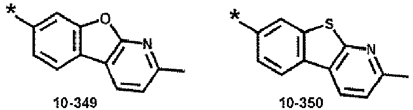
  • Formulae 10-201 to 10-350 in which at least one hydrogen is substituted with deuterium may be, for example, a group represented by one of Formulae 10-501 to 10-553:
  • the "group represented by one of Formulae 10-1 to 10-129 in which at least one hydrogen is substituted with -F" and the "group represented by one of Formulae 10-201 to 10-350 in which at least one hydrogen is substituted with -F" may be, for example, a group represented by one of Formulae 10-601 to 10-617:
  • c1 to c4, a1 to a4, e1 to e4, and d1 to d4 in Formulae 1, 2-1, and 2-2 indicate numbers of R 1 to R 4 , a group represented by *-[(L 1 ) b1 -(R 1 ) c1 ], a group represented by *-[(L 2 ) b2 -(R 2 ) c2 ], a group represented by *-[(L 3 ) b3 -(R 3 ) c3 ], a group represented by *-[(L4)b4-(R4)c4], Z 1 to Z 4 , a group represented by *-[W 1 -(Z 1 ) e1 ], a group represented by *-[W 2 -(Z 2 ) e2 ], a group represented by *-[W 3 -(Z 3 ) e3 ], and a group represented by *-[W 4 -(Z 4 ) e4 ], respectively, and may each
  • R 1 When c1 is 2 or more, two or more of R 1 (s) may be identical to or different from each other, when c2 is 2 or more, two or more of R 2 (s) may be identical to or different from each other, when c3 is 2 or more, two or more of R 3 (s) may be identical to or different from each other, when c4 is 2 or more, two or more of R 4 (s) may be identical to or different from each other, when a1 is 2 or more, two or more of groups represented by *-[(L 1 ) b1 -(R 1 ) c1 ] may be identical to or different from each other, when a2 is 2 or more, two or more of groups represented by *-[(L 2 ) b2 -(R 2 ) c2 ] may be identical to or different from each other, when a3 is 2 or more, two or more of groups represented by *-[(L 3 ) b3 -(R 3 ) c3 ] may be identical
  • the first compound and the second compound may each not be tris[2-phenyl pyridine]iridium.
  • a case where Y 1 is N, ring A 1 is a pyridine group, Y 2 is C, ring A 2 is a benzene group, and d1 and d2 are each 0 may be excluded.
  • At least one of i) two or more of a plurality of R 1 (s), ii) two or more of a plurality of R 2 (s), iii) two or more of a plurality of R 3 (s), iv) two or more of a plurality of R 4 (s), v) R 5a and R 5b , vi) two or more of a plurality of Z 1 (s), vii) two or more of a plurality of Z 2 (s), viii) two or more of a plurality of Z 3 (s), ix) two or more of a plurality of Z 4 (s), x) two or more of R 1 to R 4 , R 5a , and R 5b , and xi) two or more of Z 1 to Z 4 may each optionally bonded to each other to form a C 5 -C 30 carbocyclic group that is unsubstituted or substituted with at least one R 10a or a C 1 -
  • R 10a may be the same as described in connection with R 1 .
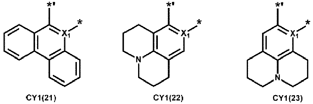
  • n1 may not be 0, n4 may be 0, and a group represented by may be a group represented by one of Formulae CY1(1) to CY1 (23): wherein, in Formulae CY1(1) to CY1(23),
  • n1 may be 1, n4 may be 0, and a group represented by may be a group represented by one of Formulae CY1-1 to CY1-18: wherein, in Formulae CY1-1 to CY1-18,
  • n1 and n2 may each be 1, and ring CY 2 may be a group represented by Formula CY2A or CY2B: wherein, in Formulae CY2A and CY2B,
  • n1 and n2 may each not be 0, and a group represented by may be a group represented by one of Formulae CY2(1) to CY2(21): wherein, in Formulae CY2(1) to CY2(21),
  • n1 and n2 may each be 1, and a group represented by may be a group represented by one of Formulae CY2-1 to CY2-16: wherein, in Formulae CY2-1 to CY2-16,
  • n2 and n3 may each not be 0, and a group represented by may be a group represented by one of Formulae CY3(1) to CY3(15): wherein, in Formulae CY3(1) to CY3(15),
  • n2 and n3 may each be 1, and a group represented by may be a group represented by one of Formulae CY3-1 to CY3-13: wherein, in Formulae CY3-1 to CY3-13,
  • n3 may not be 0, n4 may be 0, and a group represented by may be a group represented by one of Formulae CY4(1) to CY4(20): wherein, in Formulae CY4(1) to CY4(20),
  • n3 may be 1
  • n4 may be 0, and a group represented by may be a group represented by one of Formulae CY4-1 to CY4-16: wherein, in Formulae CY4-1 to CY4-16,
  • the organometallic compound represented by Formula 1 may be a compound represented by one of Formulae 1-1 to 1-3: wherein, in Formulae 1-1 to 1-3,
  • At least one of Z 11 , Z 12 , and Z 14 (for example, Z 14 ) in Formulae A1-1 to A1-3 may be:
  • Y 3 in Formula 2-2 may be N, and a group represented by in Formula 2-2 may be a group represented by one of Formulae NR1 to NR48: wherein, in Formulae NR1 to NR48,
  • the first compound may include at least one deuterium.
  • the second compound may include at least one deuterium.
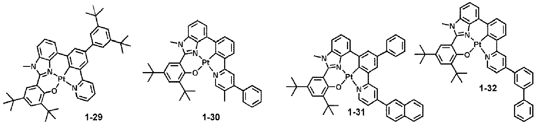
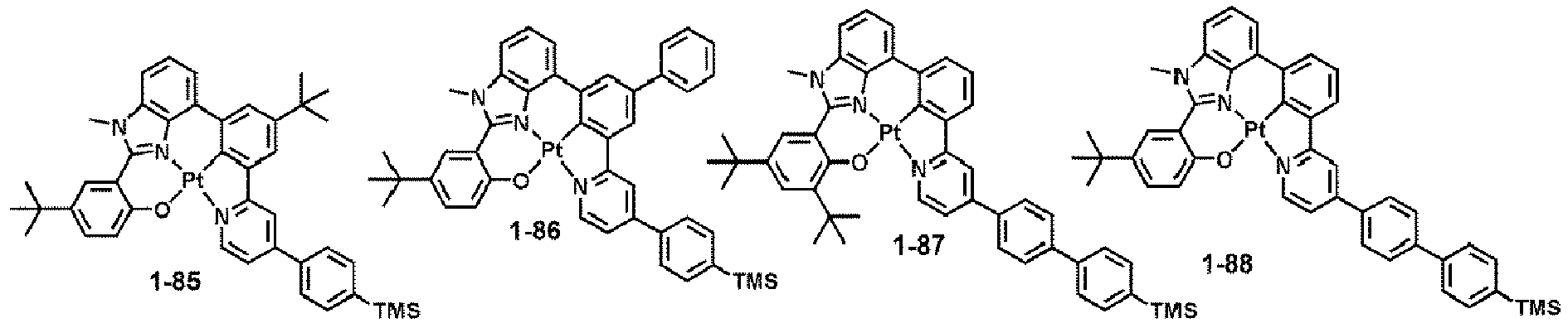
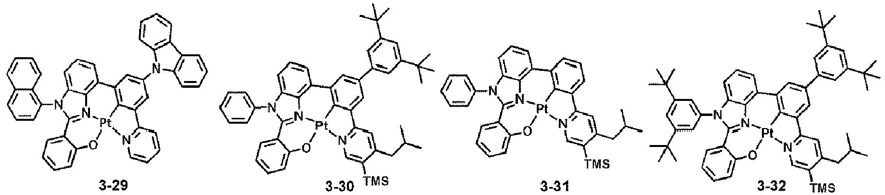
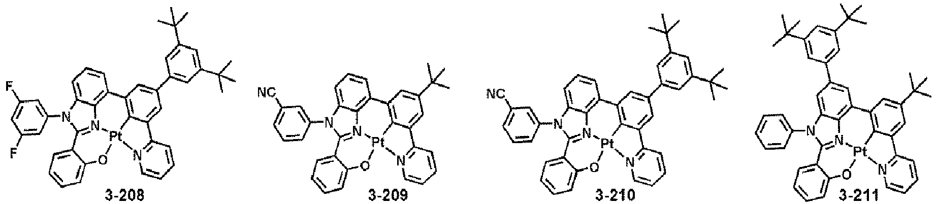
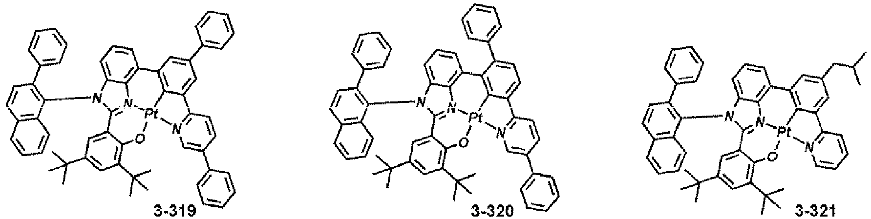
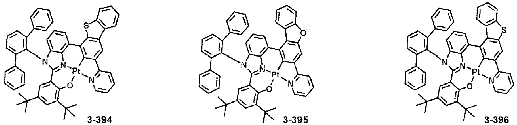
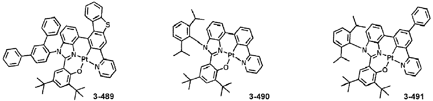
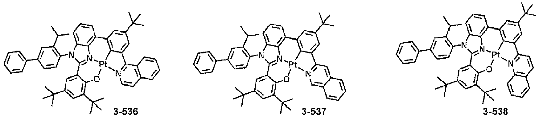
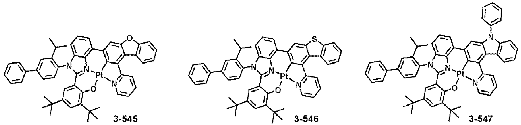
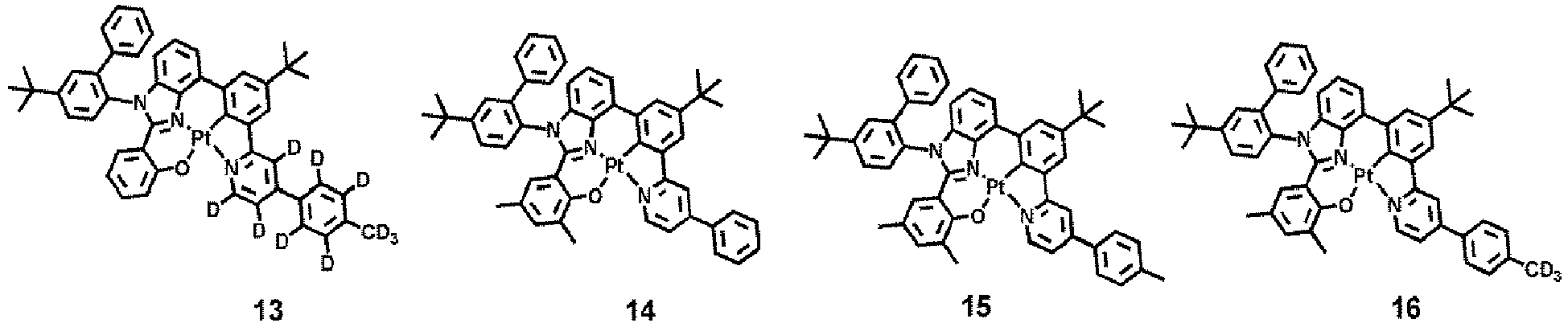
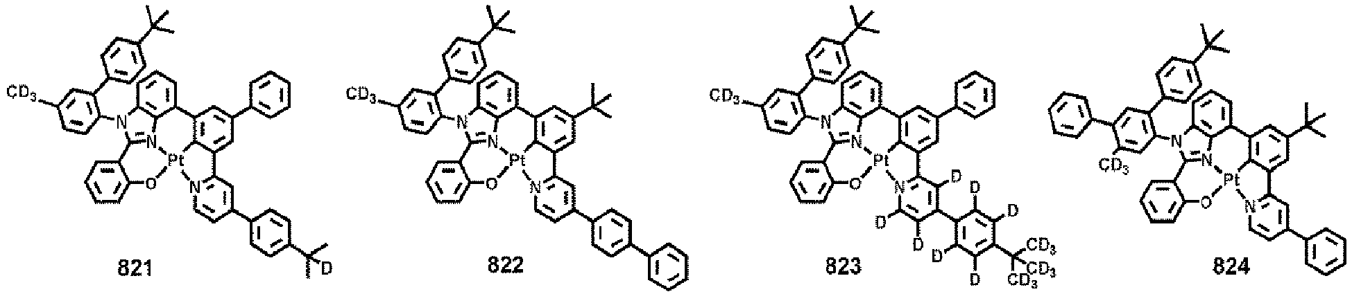
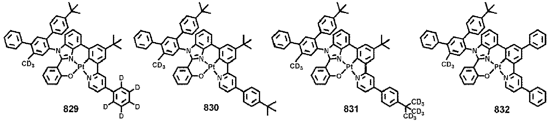
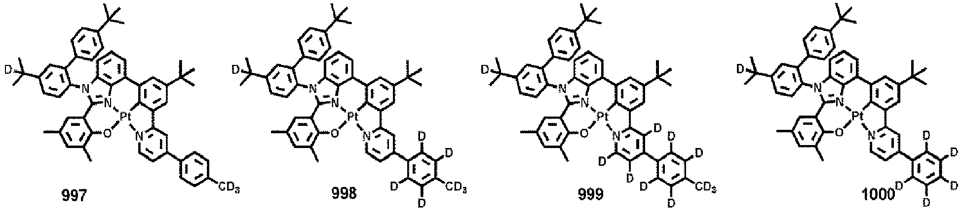
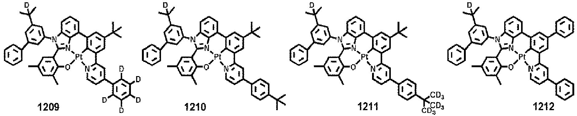
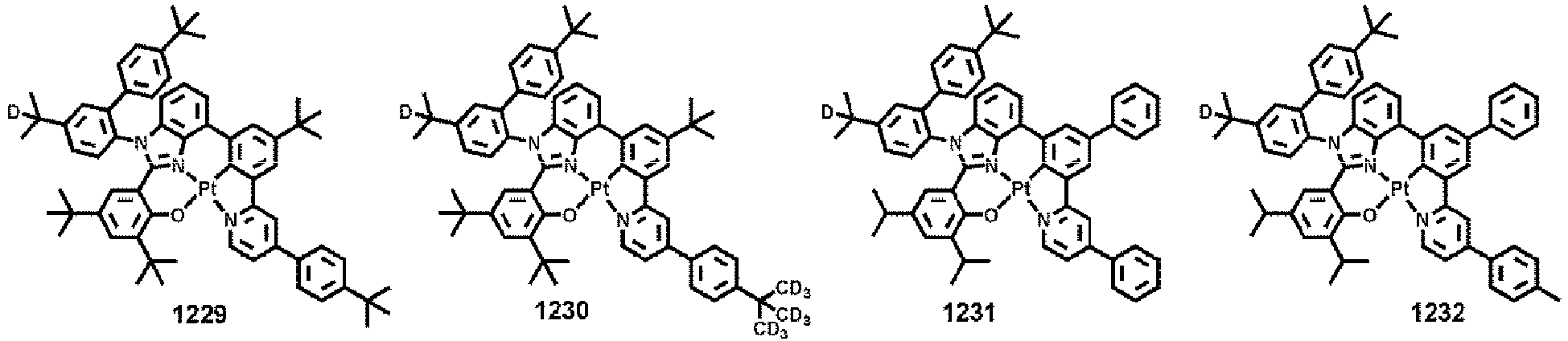
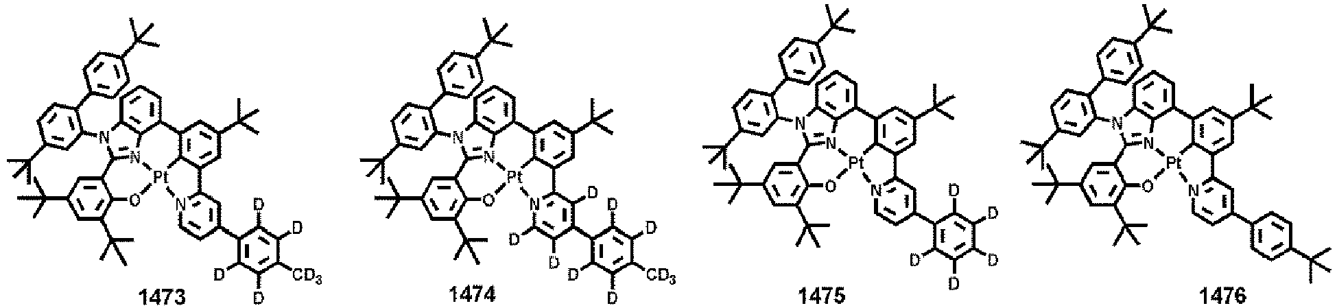
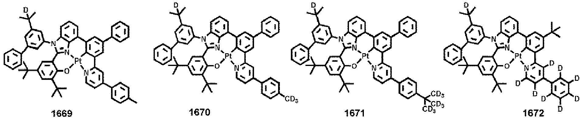
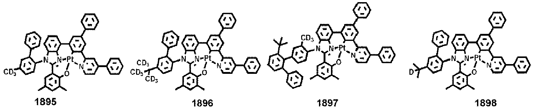
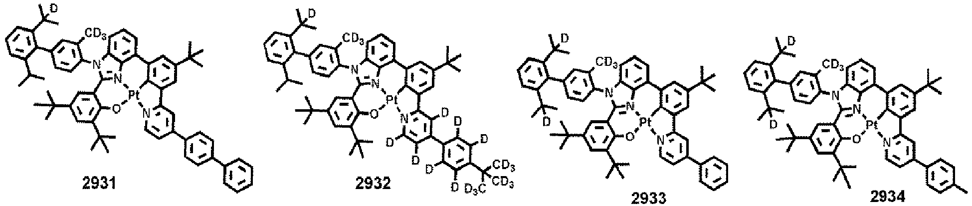
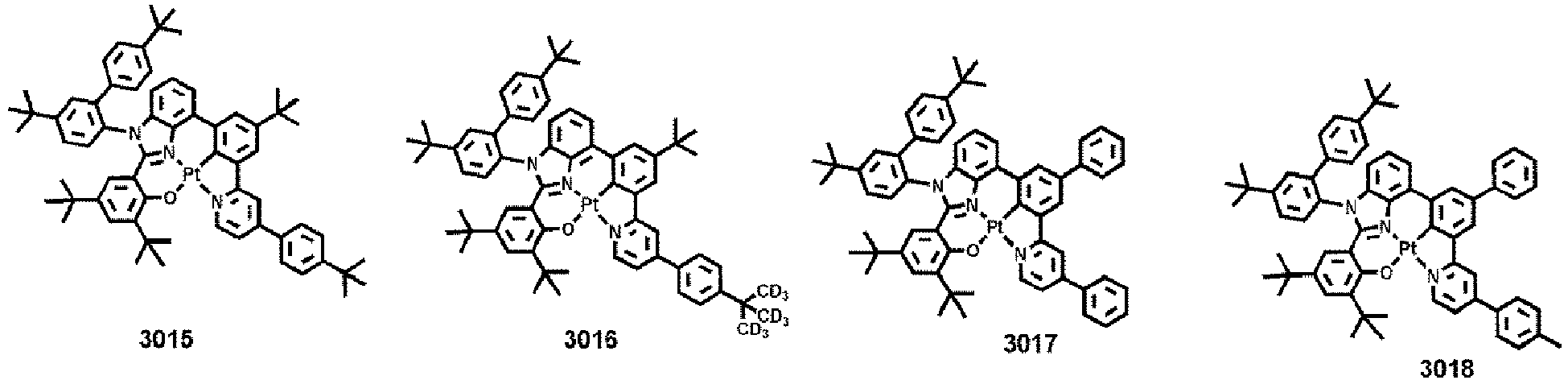
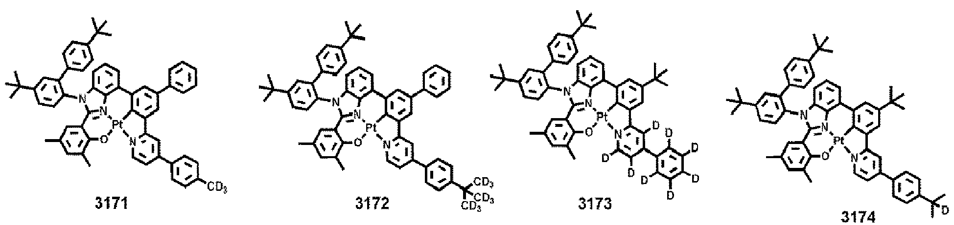
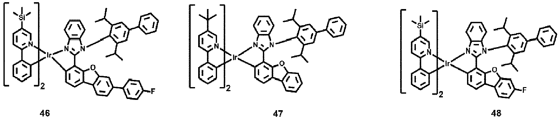
  • first compound and the second compound may each independently be selected from compounds of Group 1-1 to Group 1-4 and compounds of Group 2-1 to Group 2-5:
  • OMe refers to a methoxy group
  • TMS refers to a trimethylsilyl group
  • TMG refers to a trimethylgermyl group.
  • the first emission layer may include a first dopant and a first host
  • the second emission layer may include a second dopant and a second host
  • the first dopant may include the first compound
  • the second dopant may include the second compound
  • the first host and the second host may be identical to each other.
  • the first host and the second host may be different from each other.
  • the first host and the second host may each include a hole transport compound, an electron transport compound, a bipolar compound, or any combination thereof.
  • the first host and the second host may each include a hole transport compound and an electron transport compound, and the hole transport compound and the electron transport compound may be different from each other.
  • the hole transport compound may include at least one ⁇ electron-rich C 3 -C 60 cyclic group (e.g., a carbazole group, an indolocarbazole group, a benzene group, etc.), and may not include an electron transport group.
  • the electron transport group may include a cyano group, a fluoro group, a ⁇ electron-deficient nitrogen-containing C 1 -C 60 cyclic group, a phosphine oxide group, and a sulfoxide group.
  • the electron transport compound may be a compound including at least one electron transport group.
  • the electron transport group may be a cyano group, a fluoro group, a ⁇ electron-deficient nitrogen-containing C 1 -C 60 cyclic group, a phosphine oxide group, a sulfoxide group, or a combination thereof.
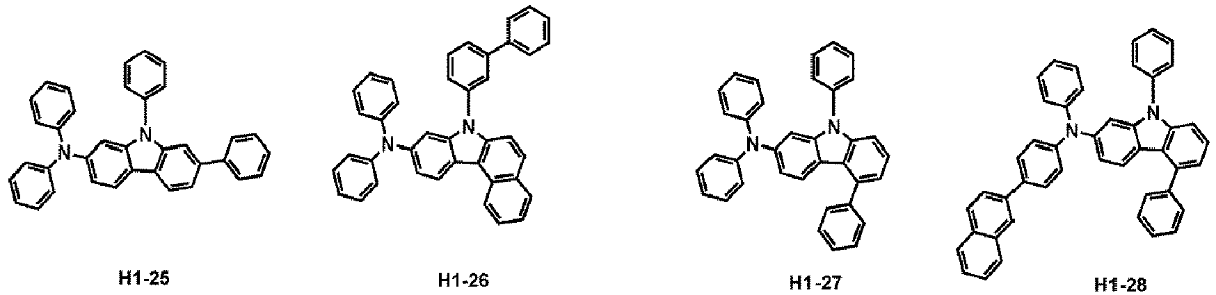
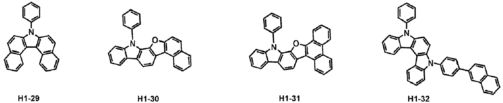
  • the hole transport compound may be at least one of Compounds H1-1 to H1-72 of Group 5-1 and Compounds H1-1 to H1-20 of Group 5-2:
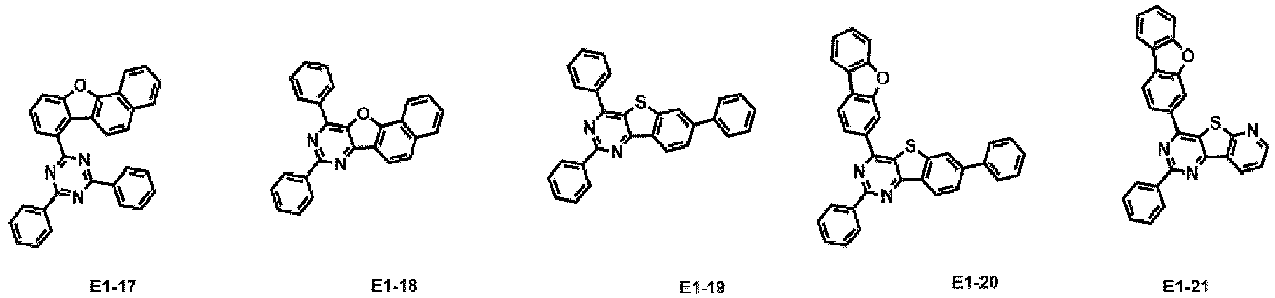
  • the electron transport compound may be at least one of Compounds E1-1 to E1-62:
  • the bipolar compound may be at least one of Compounds BP1-1 to BP1-17:
  • the emission layer may not include compounds of Group A: Group A
  • the light-emitting device may further include a hole transport region between the first electrode and the emission layer and an electron transport region between the emission layer and the second electrode.
  • the hole transport region may be the first region described in this disclosure.
  • the hole transport region may include a hole injection layer, a hole transport layer, an electron blocking layer, a buffer layer, or any combination thereof, and the electron transport region may include a hole blocking layer, an electron transport layer, an electron injection layer, or any combination thereof.
  • organic layer refers to a single layer and/or a plurality of layers between the first electrode and the second electrode of the light-emitting device.
  • the “organic layer” may include, in addition to an organic compound, an organometallic complex including metal.
  • FIG. 1 schematically illustrates a cross-sectional view of an organic light-emitting device 10, which is a light-emitting device according to an exemplary embodiment of the disclosure.
  • an organic light-emitting device 10 which is a light-emitting device according to an exemplary embodiment of the disclosure.
  • FIG. 1 schematically illustrates a cross-sectional view of an organic light-emitting device 10, which is a light-emitting device according to an exemplary embodiment of the disclosure.
  • the organic light-emitting device 10 of FIG. 1 has a structure in which a first electrode 11, a hole transport region 13, an emission layer 15, an electron transport region 17, and a second electrode 19 are sequentially stacked.
  • the emission layer 15 includes a first emission layer 15-1 and a second emission layer 15-2.
  • a substrate may be additionally located under the first electrode 11 or above the second electrode 19.
  • the substrate any substrate that is used in organic light-emitting devices available in the art may be used, and the substrate may be a glass substrate or a transparent plastic substrate, each having excellent mechanical strength, thermal stability, transparency, surface smoothness, ease of handling, and water resistance.
  • the first electrode 11 may be formed by depositing or sputtering a material for forming the first electrode 11 on the substrate.
  • the first electrode 11 may be an anode.
  • the material for forming the first electrode 11 may include materials with a high work function to facilitate hole injection.
  • the first electrode 11 may be a reflective electrode.
  • the material for forming the first electrode 11 may be indium tin oxide (ITO), indium zinc oxide (IZO), tin oxide (SnO 2 ), or zinc oxide (ZnO).
  • the material for forming the first electrode 11 may be metal, such as magnesium (Mg), aluminum (Al), silver (Ag), aluminum-lithium (Al-Li), calcium (Ca), magnesium-indium (Mg-In), or magnesium-silver (Mg-Ag).
  • metal such as magnesium (Mg), aluminum (Al), silver (Ag), aluminum-lithium (Al-Li), calcium (Ca), magnesium-indium (Mg-In), or magnesium-silver (Mg-Ag).
  • the first electrode 11 may have a single-layered structure or a multi-layered structure including two or more layers. In an embodiment, the first electrode 11 may have a three-layered structure of ITO/Ag/ITO.
  • the hole transport region 13 may be located between the first electrode 11 and the emission layer 15.
  • the hole transport region 13 may include a hole injection layer, a hole transport layer, an electron blocking layer, a buffer layer, or a combination thereof.
  • the hole transport region 13 may include only a hole injection layer or only a hole transport layer.
  • the hole transport region 13 may have a hole injection layer/hole transport layer structure or a hole injection layer/hole transport layer/electron blocking layer structure, which are sequentially stacked in this stated order from the first electrode 11.
  • the hole injection layer may be formed on the first electrode 11 by using one or more suitable methods, for example, a vacuum deposition method, a spin coating method, a casting method, a Langmuir-Blodgett (LB) method, and/or an ink-jet printing method.
  • suitable methods for example, a vacuum deposition method, a spin coating method, a casting method, a Langmuir-Blodgett (LB) method, and/or an ink-jet printing method.
  • the deposition conditions may vary depending on a material that is used to form the hole injection layer, and the structure and thermal characteristics of the hole injection layer.
  • the deposition conditions may include a deposition temperature of about 100 °C to about 500 °C, a vacuum pressure of about 10 -8 torr to about 10 -3 torr, and a deposition rate of about 0.01 ⁇ /sec to about 100 ⁇ /sec.
  • coating conditions may vary according to the material used to form the hole injection layer, and the structure and thermal properties of the hole injection layer.
  • a coating speed may be from about 2,000 rpm to about 5,000 rpm
  • a temperature at which a heat treatment is performed to remove a solvent after coating may be from about 80 °C to about 200 °C.
  • the conditions for forming the hole transport layer and the electron blocking layer may be the same as the conditions for forming the hole injection layer.
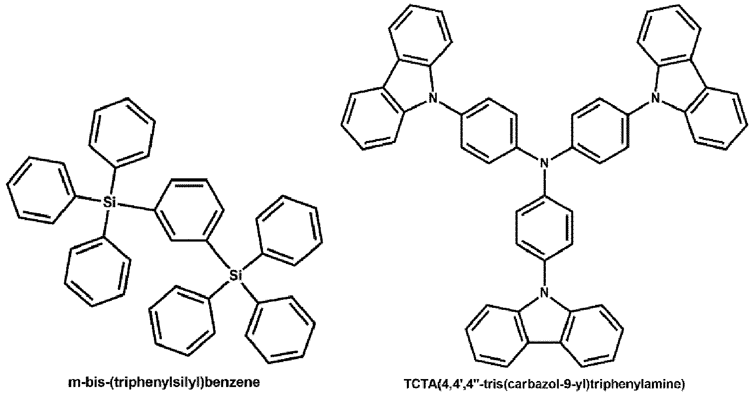
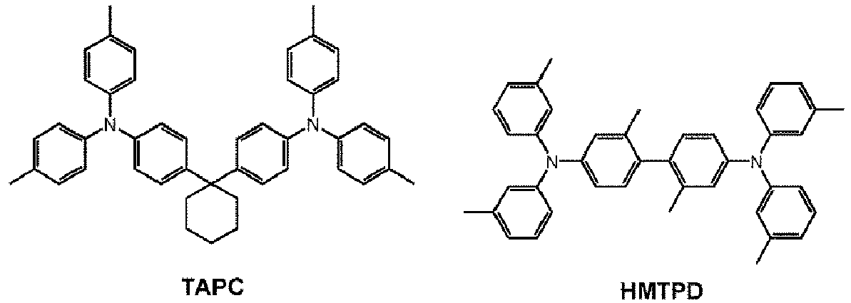
  • the hole transport region 13 may include m-MTDATA, TDATA, 2-TNATA, NPB, ⁇ -NPB, TPD, Spiro-TPD, Spiro-NPB, methylated NPB, TAPC, HMTPD, 4,4',4"-tris(N-carbazolyl)triphenylamine (TCTA), polyaniline/dodecylbenzenesulfonic acid (PANI/DBSA), poly(3,4-ethylenedioxythiophene)/poly(4-styrenesulfonate) (PEDOT/PSS), polyaniline/camphor sulfonic acid (PANI/CSA), polyaniline/poly(4-styrenesulfonate) (PANI/PSS), a compound represented by Formula 201 below, a compound represented by Formula 202 below, or any combination thereof:
  • Ar 101 and Ar 102 may each independently be a phenylene group, a pentalenylene group, an indenylene group, a naphthylene group, an azulenylene group, a heptalenylene group, an acenaphthylene group, a fluorenylene group, a phenalenylene group, a phenanthrenylene group, an anthracenylene group, a fluoranthenylene group, a triphenylenylene group, a pyrenylene group, a chrysenylenylene group, a naphthacenylene group, a picenylene group, a perylenylene group, or a pentacenylene group, each unsubstituted or substituted with deuterium, -F, -CI, -Br, -I, a hydroxyl group, a cyano group, a nitro group, an
  • xa and xb in Formula 201 may each independently be an integer from 0 to 5, or 0, 1, or 2.
  • xa may be 1 and xb may be 0.
  • R101 to R 108 , R 111 to R 119 , and R121 to R124 in Formulae 201 and 202 may each independently be:
  • R 109 may be a phenyl group, a naphthyl group, an anthracenyl group, or a pyridinyl group, each unsubstituted or substituted with deuterium, -F, -CI, -Br, -I, a hydroxyl group, a cyano group, a nitro group, an amino group, a C 1 -C 20 alkyl group, a C 1 -C 20 alkoxy group, a phenyl group, a naphthyl group, an anthracenyl group, a pyridinyl group, or any combination thereof.
  • the compound represented by Formula 201 may be represented by Formula 201A: wherein R101, R111, R112, and R 109 in Formula 201A are each the same as described above.
  • the hole transport region 13 may include one of Compounds HT1 to HT20 or any combination thereof:
  • a thickness of the hole transport region 13 may be from about 100 ⁇ to about 10,000 ⁇ , for example, from about 100 ⁇ to about 1,000 ⁇ .
  • a thickness of the hole injection layer may be in a range of about 100 ⁇ to about 10,000 ⁇ , for example, about 100 ⁇ to about 1,000 ⁇ , and a thickness of the hole transport layer may be in a range of about 50 ⁇ to about 2,000 ⁇ , for example, about 100 ⁇ to about 1,500 ⁇ .
  • the thicknesses of the hole transport region 13, the hole injection layer, and the hole transport layer are within these ranges, satisfactory hole transporting characteristics may be obtained without a substantial increase in driving voltage.
  • the hole transport region 13 may further include a charge-generation material to improve conductivity.
  • the charge-generation material may be homogeneously or non-homogeneously dispersed in the hole transport region.
  • the charge-generation material may be, for example, a p-dopant.
  • the p-dopant may be a quinone derivative, a metal oxide, a cyano group-containing compound, or any combination thereof.
  • the p-dopant may be: a quinone derivative such as tetracyanoquinonedimethane (TCNQ), 2,3,5,6-tetrafluoro-tetracyano-1,4-benzoquinonedimethane (F4-TCNQ), or F6-TCNNQ; metal oxide, such as tungsten oxide and molybdenum oxide; a cyano group-containing compound, such as Compound HT-D1; or any combination thereof:
  • the hole transport region 13 may further include a buffer layer.
  • the buffer layer may compensate for an optical resonance distance according to a wavelength of light emitted from the emission layer, and thus, luminescence efficiency of a light-emitting device may be improved.
  • the material for the electron blocking layer may include a material, a host material, or a combination thereof that can be used in the hole transport region 13 as described above.
  • the hole transport region includes an electron blocking layer, mCP, Compound H1-8 of Group 5-2, or the like may be used as a material for the electron blocking layer.
  • the emission layer 15 may be formed on the hole transport region 13 by using, for example, a vacuum deposition method, a spin coating method, a cast method, an LB method, and/or an ink-jet printing method.
  • a vacuum deposition method or a spin coating method
  • the deposition or coating conditions may be similar to those applied in forming the hole injection layer although the deposition or coating conditions may vary depending on a material that is used to form the emission layer.
  • the emission layer 15 may include a first emission layer 15-1 and a second emission layer 15-2 as described herein.
  • the first emission layer 15-1 may include a first dopant and a first host
  • the second emission layer 15-2 may include a second dopant and a second host
  • the first dopant may include the first compound
  • the second dopant may include the second compound.
  • the first dopant, the first host, the second dopant, the second host, the first compound, and the second compound are each the same as described in the present specification.
  • An amount (weight) of the first dopant in the first emission layer 15-1 may be from about 0.01 parts by weight to about 20 parts by weight based on 100 parts by weight, based on the total weight of the first host.
  • An amount (weight) of the second dopant in the second emission layer 15-2 may be from about 0.01 parts by weight to about 20 parts by weight based on 100 parts by weight, based on the total weight of the second host.
  • a thickness of the emission layer 15 may be in a range of about 100 ⁇ to about 1,000 ⁇ , for example, about 200 ⁇ to about 600 ⁇ . When the thickness of the emission layer 15 is within these ranges, excellent light-emission characteristics may be obtained without a substantial increase in driving voltage.
  • a thickness ratio of the first emission layer 15-1 to the second emission layer 15-2 may be 8 : 2 to 2 : 8, 7 : 3 to 3 : 7, or 6 : 4 to 4 : 6.
  • the emission layer 15 may be patterned into a red emission layer, a green emission layer, and/or a blue emission layer.
  • the electron transport region 17 may be located on the emission layer 15.
  • the electron transport region 17 may include a hole blocking layer, an electron transport layer, an electron injection layer, or a combination thereof.
  • the electron transport region 17 may have a hole blocking layer/electron transport layer/electron injection layer structure or an electron transport layer/electron injection layer structure.
  • the electron transport layer may have a single-layered structure or a multi-layered structure including two or more different materials.
  • the conditions for the formation of the hole blocking layer, the electron transport layer, and the electron injection layer in the electron transport region 17 are the same as the conditions for the formation of the hole injection layer.
  • the hole blocking layer may include, for example, BCP, Bphen, BAIq, or any combination thereof:
  • the hole blocking layer may include any host material, and a material for an electron transport layer, a material for an electron injection layer, or a combination thereof, which will be described later.
  • a thickness of the hole blocking layer may be in a range of about 20 ⁇ to about 1,000 ⁇ , for example, about 30 ⁇ to about 600 ⁇ . When the thickness of the hole blocking layer is within these ranges, excellent hole blocking characteristics may be obtained without a substantial increase in driving voltage.
  • the electron transport layer may include BCP, Bphen, TPBi, Alq 3 , BAIq, TAZ, NTAZ, or any combination thereof:
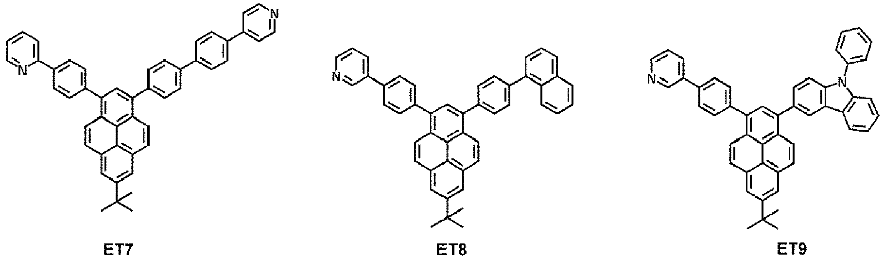
  • the electron transport layer may include one of Compounds ET1 to ET25 or any combination thereof:
  • a thickness of the electron transport layer may be in the range of about 100 ⁇ to about 1,000 ⁇ , for example, about 150 ⁇ to about 500 ⁇ . When the thickness of the electron transport layer is within the range described above, the electron transport layer may have satisfactory electron transporting characteristics without a substantial increase in driving voltage.
  • the electron transport layer may include a metal-containing material in addition to the material as described above.
  • the metal-containing material may include a Li complex.
  • the Li complex may include, for example, Compound ET-D1 or ET-D2:
  • the electron transport region 17 may include an electron injection layer that facilitates injection of electrons from the second electrode 19.
  • the electron injection layer may include LiF, NaCl, CsF, Li 2 O, BaO, Yb, Compound ET-D1, Compound ET-D2, or any combination thereof.
  • a thickness of the electron injection layer may be in a range of about 1 ⁇ to about 100 ⁇ , and, for example, about 3 ⁇ to about 90 ⁇ . When the thickness of the electron injection layer is within the range described above, satisfactory electron injection characteristics may be obtained without a substantial increase in driving voltage.
  • the second electrode 19 may be provided on the electron transport region 17.
  • the second electrode 19 may be a cathode.
  • a material for forming the second electrode 19 may be metal, an alloy, an electrically conductive compound, or a combination thereof, which have a relatively low work function.
  • lithium (Li), magnesium (Mg), aluminum (Al), silver (Ag), aluminum-lithium (Al-Li), calcium (Ca), magnesium-indium (Mg-In), magnesium-silver (Mg-Ag), or the like may be used as the material for forming the second electrode 19.
  • a transparent or semi-transparent electrode formed using ITO or IZO may be used as the second electrode 19.
  • the light-emitting device may be included in an electronic apparatus.
  • an electronic apparatus including the light-emitting device is provided.
  • the electronic apparatus may include, for example, a display, an illumination, a sensor, and the like.
  • C 1 -C 60 alkyl group refers to a linear or branched saturated aliphatic hydrocarbons monovalent group having 1 to 60 carbon atoms
  • C 1 -C 60 alkylene group refers to a divalent group having the same structure as the C 1 -C 60 alkyl group.
  • Examples of the C 1 -C 60 alkyl group, the C 1 -C 20 alkyl group, and/or the C 1 -C 10 alkyl group may include a methyl group, an ethyl group, an n-propyl group, an isopropyl group, an n-butyl group, a sec-butyl group, an isobutyl group, a tert-butyl group, an n-pentyl group, a tert-pentyl group, a neopentyl group, an isopentyl group, a sec-pentyl group, a 3-pentyl group, a sec-isopentyl group, an n-hexyl group, an isohexyl group, a sec-hexyl group, a tert-hexyl group, an n-heptyl group, an isoheptyl group, a sec-heptyl group, a
  • C 1 -C 60 alkoxy group refers to a monovalent group represented by -OA 101 (wherein A 101 is the C 1 -C 60 alkyl group), and examples thereof may include a methoxy group, an ethoxy group, a propoxy group, a butoxy group, a pentoxy group, or the like.
  • C 1 -C 60 alkylthio group refers to a monovalent group having the formula of -SA 101 (where A 101 is the C 1 -C 60 alkyl group).
  • C 2 -C 60 alkenyl group refers to a hydrocarbon group formed by substituting at least one carbon-carbon double bond in the middle or at the terminus of the C 2 -C 60 alkyl group, and examples thereof include an ethenyl group, a propenyl group, a butenyl group, or the like.
  • C 2 -C 60 alkenylene group refers to a divalent group having the same structure as the C 2 -C 60 alkenyl group.
  • C 2 -C 60 alkynyl group refers to a hydrocarbon group formed by substituting at least one carbon-carbon triple bond in the middle or at the terminus of the C 2 -C 60 alkyl group, and examples thereof include an ethynyl group, a propynyl group, or the like.
  • C 2 -C 60 alkynylene group refers to a divalent group having the same structure as the C 2 -C 60 alkynyl group.
  • C 3 -C 10 cycloalkyl group refers to a monovalent saturated hydrocarbon cyclic group having 3 to 10 carbon atoms, and the C 3 -C 10 cycloalkylene group is a divalent group having the same structure as the C 3 -C 10 cycloalkyl group.
  • Examples of the C 3 -C 10 cycloalkyl group may include a cyclopropyl group, a cyclobutyl group, a cyclopentyl, cyclohexyl group, a cycloheptyl group, a cyclooctyl group, an adamantanyl group, a norbornanyl group (or a bicyclo[2.2.1]heptyl group), a bicyclo[1.1.1]pentyl group, a bicyclo[2.1.1]hexyl group, a bicyclo[2.2.2]octyl group, or the like.
  • C 1 -C 10 heterocycloalkyl group refers to a monovalent saturated cyclic group that includes at least one hetero atom selected from N, O, P, Si, S, Se, Ge, and B as a ring-forming atom and 1 to 10 carbon atoms
  • C 1 -C 10 heterocycloalkylene group refers to a divalent group having the same structure as the C 1 -C 10 heterocycloalkyl group.
  • Examples of the C 1 -C 10 heterocycloalkyl group may include a silolanyl group, a silinanyl group, a tetrahydrofuranyl group, a tetrahydro-2H-pyranyl group, a tetrahydrothiophenyl group, or the like.
  • C 3 -C 10 cycloalkenyl group refers to a monovalent monocyclic group that has 3 to 10 carbon atoms and at least one carbon-carbon double bond in the ring thereof and no aromaticity, and non-limiting examples thereof include a cyclopentenyl group, a cyclohexenyl group, a cycloheptenyl group, or the like.
  • C 3 -C 10 cycloalkenylene group refers to a divalent group having the same structure as the C 3 -C 10 cycloalkenyl group.
  • C 1 -C 10 heterocycloalkenyl group refers to a monovalent monocyclic group that has at least one hetero atom selected from N, O, P, Si, S, Se, Ge, and B as a ring-forming atom, 1 to 10 carbon atoms, and at least one double bond in its ring.
  • Examples of the C 1 -C 10 heterocycloalkenyl group include a 2,3-dihydrofuranyl group, a 2,3-dihydrothiophenyl group, or the like.
  • C 1 -C 10 heterocycloalkenylene group refers to a divalent group having the same structure as the C 1 -C 10 heterocycloalkenyl group.
  • C 6 -C 60 aryl group refers to a monovalent group having a carbocyclic aromatic system having 6 to 60 carbon atoms
  • C 6 -C 60 arylene group refers to a divalent group having a carbocyclic aromatic system having 6 to 60 carbon atoms.
  • Examples of the C 6 -C 60 aryl group include a phenyl group, a naphthyl group, an anthracenyl group, a phenanthrenyl group, a pyrenyl group, a chrysenyl group, or the like.
  • the C 6 -C 60 aryl group and the C 6 -C 60 arylene group each include two or more rings, the rings may be fused to each other.
  • the C 7 -C 60 alkylaryl group used herein refers to a C 6 -C 60 aryl group substituted with at least one C 1 -C 60 alkyl group.
  • C 1 -C 60 heteroaryl group refers to a monovalent group that includes at least one hetero atom selected from N, O, P, Si, S, Se, Ge, and B as a ring-forming atom and a cyclic aromatic system having 1 to 60 carbon atoms
  • C 1 -C 60 heteroarylene group refers to a divalent group that includes at least one hetero atom selected from N, O, P, Si, S, Se, Ge, and B as a ring-forming atom and a cyclic aromatic system having 1 to 60 carbon atoms.
  • Examples of the C 1 -C 60 heteroaryl group include a pyridinyl group, a pyrimidinyl group, a pyrazinyl group, a pyridazinyl group, a triazinyl group, a quinolinyl group, and an isoquinolinyl group.
  • the C 6 -C 60 heteroaryl group and the C 6 -C 60 heteroarylene group each include two or more rings, the two or more rings may be fused to each other.
  • the C 2 -C 60 alkylheteroaryl group used herein refers to a C 1 -C 60 heteroaryl group substituted with at least one C 1 -C 60 alkyl group.
  • C 6 -C 60 aryloxy group indicates -OA 102 (wherein A 102 indicates the C 6 -C 60 aryl group), the C 6 -C 60 arylthio group indicates -SA 103 (wherein A 103 indicates the C 6 -C 60 aryl group), and the C 1 -C 60 alkylthio group indicates -SA 104 (wherein A 104 indicates the C 1 -C 60 alkyl group).
  • the term "monovalent non-aromatic condensed polycyclic group” as used herein refers to a monovalent group (for example, having 8 to 60 carbon atoms) having two or more rings condensed to each other, only carbon atoms as ring-forming atoms, and no aromaticity in its entire molecular structure.
  • Examples of the monovalent non-aromatic condensed polycyclic group include a fluorenyl group.
  • divalent non-aromatic condensed polycyclic group refers to a divalent group having the same structure as a monovalent non-aromatic condensed polycyclic group.
  • the term "monovalent non-aromatic condensed heteropolycyclic group” as used herein refers to a monovalent group (for example, having 1 to 60 carbon atoms) having two or more rings condensed to each other, including at least one hetero atom selected from N, O, P, Si, S, Se, Ge, and B, other than carbon atoms, as a ring-forming atom, and having no aromaticity in its entire molecular structure.
  • Examples of the monovalent non-aromatic condensed heteropolycyclic group include a carbazolyl group or the like.
  • divalent non-aromatic condensed heteropolycyclic group refers to a divalent group having the same structure as a monovalent non-aromatic condensed heteropolycyclic group.
  • C 5 -C 30 carbocyclic group refers to a saturated or unsaturated cyclic group having, as a ring-forming atom, 5 to 30 carbon atoms only.
  • the C 5 -C 30 carbocyclic group may be a monocyclic group or a polycyclic group.
  • Examples of the "C 5 -C 30 carbocyclic group (unsubstituted or substituted with at least one R 10a )" used herein may include an adamantane group, a norbornene group, a bicyclo[1.1.1]pentane group, a bicyclo[2.1.1]hexane group, a bicyclo[2.2.1]heptane(norbornane) group, a bicyclo[2.2.2]octane group, a cyclopentane group, a cyclohexane group, a cyclohexene group, a benzene group, a naphthalene group, an anthracene group, a phenanthrene group, a triphenylene group, a pyrene group, a chrysene group, a 1,2,3,4-tetrahydronaphthalene group, a cyclopentadiene group, and a fluorene
  • C 1 -C 30 heterocyclic group refers to a saturated or unsaturated cyclic group having, as a ring-forming atom, at least one heteroatom selected from N, O, P, Si, S, Se, Ge, and B other than 1 to 30 carbon atoms.
  • the C 1 -C 30 heterocyclic group may be a monocyclic group or a polycyclic group.
  • the "C 1 -C 30 heterocyclic group (unsubstituted or substituted with at least one R 10a )" may be, for example, a thiophene group, a furan group, a pyrrole group, a silole group, borole group, a phosphole group, a selenophene group, a germole group, a benzothiophene group, a benzofuran group, an indole group, a benzosilole group, a benzoborole group, a benzophosphole group, a benzoselenophene group, a benzogermole group, a dibenzothiophene group, a dibenzofuran group, a carbazole group, a dibenzosilole group, a dibenzoborole group, a dibenzophosphole group, a dibenzoselenophene group, a dibenzogermole group, a dibenzo
  • the number of carbons in each group that is substituted excludes the number of carbons in the substituent.
  • a C 1 -C 60 alkyl group can be substituted with a C 1 -C 60 alkyl group.
  • the total number of carbons included in the C 1 -C 60 alkyl group substituted with the C 1 -C 60 alkyl group is not limited to 60 carbons.
  • more than one C 1 -C 60 alkyl substituent may be present on the C 1 -C 60 alkyl group. This definition is not limited to the C 1 -C 60 alkyl group and applies to all substituted groups that recite a carbon range.
  • examples of the "C 5 -C 30 carbocyclic group” and "C 1 -C 30 heterocyclic group” as used herein include i) a first ring, ii) a second ring, iii) a condensed ring in which two or more first rings are condensed with each other, iv) a condensed ring in which two or more second rings are condensed with each other, or v) a condensed ring in which at least one first ring and at least one second ring are condensed with each other,
  • fluorinated C 1 -C 60 alkyl group (or a fluorinated C 1 -C 20 alkyl group or the like)
  • fluorinated C 3 -C 10 cycloalkyl group "fluorinated C 1 -C 10 heterocycloalkyl group”
  • fluorinated phenyl group respectively indicate a C 1 -C 60 alkyl group (or a C 1 -C 20 alkyl group or the like), a C 3 -C 10 cycloalkyl group, a C 1 -C 10 heterocycloalkyl group, and a phenyl group, each substituted with at least one fluoro group (-F).
  • fluorinated C 1 alkyl group that is, a fluorinated methyl group
  • fluorinated C 1 alkyl group includes -CF 3 , -CF 2 H, and -CFH 2 .
  • the "fluorinated C 1 -C 60 alkyl group (or, a fluorinated C 1 -C 20 alkyl group, or the like)", "the fluorinated C 3 -C 10 cycloalkyl group", “the fluorinated C 1 -C 10 heterocycloalkyl group”, or “the fluorinated phenyl group” may be i) a fully fluorinated C 1 -C 60 alkyl group (or, a fully fluorinated C 1 -C 20 alkyl group, or the like), a fully fluorinated C 3 -C 10 cycloalkyl group, a fully fluorinated C 1 -C 10 heterocycloalkyl group, or a fully fluorinated phenyl group,
  • deuterated C 1 -C 60 alkyl group (or a deuterated C 1 -C 20 alkyl group or the like)
  • deuterated C 3 -C 10 cycloalkyl group "deuterated C 1 -C 10 heterocycloalkyl group”
  • deuterated phenyl group respectively indicate a C 1 -C 60 alkyl group (or a C 1 -C 20 alkyl group or the like), a C 3 -C 10 cycloalkyl group, a C 1 -C 10 heterocycloalkyl group, and a phenyl group, each substituted with at least one deuterium.
  • the "deuterated C 1 alkyl group (that is, the deuterated methyl group)" may include - CD 3 , -CD 2 H, and -CDH 2 , and examples of the “deuterated C 3 -C 10 cycloalkyl group” are, for example, Formula 10-501 and the like.
  • the "deuterated C 1 -C 60 alkyl group (or, the deuterated C 1 -C 20 alkyl group or the like)", “the deuterated C 3 -C 10 cycloalkyl group”, “the deuterated C 1 -C 10 heterocycloalkyl group”, or “the deuterated phenyl group” may be i) a fully deuterated C 1 -C 60 alkyl group (or, a fully deuterated C 1 -C 20 alkyl group or the like), a fully deuterated C 3 -C 10 cycloalkyl group, a fully deuterated C 1 -C 10 heterocycloalkyl group, or a fully deuterated phenyl group, in which, in each group, all hydrogen included therein are substituted with deuterium, or ii) a partially deuterated C 1 -C 60 alkyl group (or, a partially deuterated C 1 -C 20 alkyl group or the like), a partially deuterated
  • (C 1 -C 20 alkyl) 'X' group refers to a 'X' group that is substituted with at least one C 1 -C 20 alkyl group.
  • the term "(C 1 -C 20 alkyl)C 3 -C 10 cycloalkyl group” as used herein refers to a C 3 -C 10 cycloalkyl group substituted with at least one C 1 -C 20 alkyl group
  • the term “(C 1 -C 20 alkyl)phenyl group” as used herein refers to a phenyl group substituted with at least one C 1 -C 20 alkyl group.
  • An example of a (C 1 alkyl) phenyl group is a toluyl group.
  • Q 1 to Q9, Q 11 to Q 19 , Q 21 to Q29, and Q31 to Q39 described herein may each independently be:
  • Compound HT(1) is a compound which is identical to Compound H1-8 of Group 5-2.
  • an emission spectrum of each of the films A and B was measured using a Quantaurus-QY Absolute PL quantum yield spectrometer of Hamamatsu company (on which a xenon light source, a monochromator, a photonic multichannel analyzer, and an integrating sphere are mounted and which includes PLQY measurement software (Hamamatsu Photonics, Ltd., Shizuoka, Japan).
  • a Quantaurus-QY Absolute PL quantum yield spectrometer of Hamamatsu company (on which a xenon light source, a monochromator, a photonic multichannel analyzer, and an integrating sphere are mounted and which includes PLQY measurement software (Hamamatsu Photonics, Ltd., Shizuoka, Japan).
  • an excitation wavelength was scanned from 320 nm to 380 nm at 10 nm intervals, and a spectrum measured at the excitation wavelength of 320 nm was taken.
  • an ITO-patterned glass substrate was cut to a size of 50 mm x 50 mm x 0.5 mm, sonicated with isopropyl alcohol and pure water, each for 5 minutes, and then cleaned by irradiation of ultraviolet rays and exposure of ozone thereto for 30 minutes.
  • the resultant glass substrate was loaded onto a vacuum deposition apparatus.
  • HT3 and F6-TCNNQ were vacuum-codeposited on the anode at a weight ratio of 98 : 2 to form a hole injection layer having a thickness of 10 nm
  • HT3 was vacuum-deposited on the hole injection layer to form a hole transport layer having a thickness of 135 nm
  • HT(1) was vacuum-deposited on the hole transport layer to form an electron blocking layer having a thickness of 30 nm.
  • ET3 and ET-D1 were co-deposited on the emission layer EA at a volume ratio of 50 : 50 to form an electron transport layer having a thickness of 35 nm, ET-D1 was vacuum-deposited on the electron transport layer to form an electron injection layer having a thickness of 1 nm, and then Al was vacuum-deposited on the electron injection layer to form a cathode having a thickness of 100 nm, thereby completing manufacture of a light-emitting device A.
  • a light-emitting device B was manufactured in the same manner as used to manufacture the light-emitting device A, except that compounds shown in Table 2 were co-deposited on the electron blocking layer at a weight ratio shown in Table 2 to form an emission layer EB having a thickness of 40 nm instead of the emission layer EA.
  • Emission layer composition (weight ratio) Current density at 5.5 V (mA/cm 2 )
  • the current density (at 5.5 V) of the light-emitting device B including only the emission layer EB as an emission layer is greater than the current density (at 5.5 V) of the light-emitting device A including only the emission layer EA as an emission layer.
  • a glass substrate with ITO/Ag/ITO deposited thereon to a thickness of 70/1,000/70 ⁇ was cut to a size of 50 mm x 50 mm x 0.5 mm, sonicated with isopropyl alcohol and pure water each for 5 minutes, and then cleaned by irradiation of ultraviolet rays and exposure of ozone thereto for 30 minutes. Then the resultant glass substrate was loaded onto a vacuum deposition apparatus.
  • HT3 and F6-TCNNQ were vacuum-codeposited on the anode at a weight ratio of 98 : 2 to form a hole injection layer having a thickness of 10 nm
  • HT3 was vacuum-deposited on the hole injection layer to form a hole transport layer having a thickness of 128 nm
  • HT(1) was vacuum-deposited on the hole transport layer to form an electron blocking layer having a thickness of 30 nm.
  • a dopant (GD-A) and a host (HT(1) and E1-62) were co-deposited on the electron blocking layer to form a first emission layer having a thickness of 15 nm
  • a dopant (GD-B) and a host (HT(1) and E1-62) were co-deposited on the first emission layer to form a second emission layer having a thickness of 18 nm, thereby completing manufacture of an emission layer.
  • An amount of the dopant in the first emission layer was 10 parts by weight based on 100 parts by weight of the first emission layer, an amount of the dopant in the second emission layer was 5 parts by weight based on 100 parts by weight of the second emission layer, and a weight ratio of HT(1) and E1-62 in the first emission layer and the second emission layer was 7 : 3.
  • ET3 and ET-D1 were co-deposited on the emission layer at a volume ratio of 50 : 50 to form an electron transport layer having a thickness of 35 nm
  • LiF was vacuum-deposited on the electron transport layer to form an electron injection layer having a thickness of 1 nm
  • Mg and Ag were co-deposited on the electron injection layer at a weight ratio of 90 :10 to form a cathode having a thickness of 12 nm, thereby completing manufacture of a light-emitting device.
  • OLEDs 1-2 to 1-4 were manufactured in the same manner as used to manufacture the OLED 1-1, except that the thickness of the hole transport layer was changed as shown in Table 3 below.
  • Table 3 OLED 1-1 OLED 1-2 OLED 1-3 OLED 1-4
  • Dopant GD-B Amount of dopant 5 parts by weight based on 100 parts by weight of second emission layer Host composition (weight ratio) HT(1) : E1-62 (7 : 3) Thickness 18 nm
  • Dopant GD-A Amount of dopant 10 parts by weight based on 100 parts by weight of first emission layer Host composition (weight ratio) HT(1) : E1-62 (7 : 3) Thickness 15 nm Hole transport layer Thickness of hole transport layer 128 nm 132 nm 136 nm 140 nm
  • OLEDs C1-1 to C1-4 were manufactured in the same manner as used to manufacture the OLEDs 1-1 to 1-4, except that the configuration of the emission layer was changed as shown in Table 4 below.
  • Table 4 OLED C1-1 OLED C1-2 OLED C1-3 OLED C1-4 cathode Composition Mg : Ag (90 : 10) Thickness 12 nm Emission layer Dopant GD-A Amount of dopant 10 parts by weight based on 100 parts by weight of emission layer Host composition (weight ratio) HT(1) : E1-62 (7 : 3) Thickness 33 nm Hole transport layer Thickness of hole transport layer 128 nm 132 nm 136 nm 140 nm Anode (reflective electrode) Composition and thickness ITO / Ag / ITO (70 ⁇ / 1,000 ⁇ / 70 ⁇ ) Manufacture of OLEDs C2-1 to C2-4
  • OLEDs C2-1 to C2-4 were manufactured in the same manner as used to manufacture the OLEDs 1-1 to 1-4, except that the configuration of the emission layer was changed as shown in Table 5 below.
  • Table 5 OLED C2-1 OLED C2-2 OLED C2-3 OLED C2-4
  • Dopant GD-B Amount of dopant 5 parts by weight based on 100 parts by weight of emission layer Host composition (weight ratio) HT(1) : E1-62 (7 : 3) Thickness 33 nm Hole transport layer Thickness of hole transport layer 128 nm 132 nm 136 nm 140 nm
  • OLEDs C3-1 to C3-4 were manufactured in the same manner as used to manufacture the OLEDs 1-1 to 1-4, except that the configuration of the emission layer was changed as shown in Table 6 below.
  • Table 6 OLED C3-1 OLED C3-2 OLED C3-3 OLED C3-4
  • Dopant GD-A Amount of dopant 10 parts by weight based on 100 parts by weight of second emission layer Host composition (weight ratio) HT(1) : E1-62 (7 : 3) Thickness 18 nm
  • Dopant GD-B Amount of dopant 5 parts by weight based on 100 parts by weight of first emission layer Host composition (weight ratio) HT(1) : E1-62 (7 : 3) Thickness 15 nm Hole transport layer Thickness of hole transport layer 128 nm 132 nm 136 nm 140 nm
  • an emission peak wavelength (nm) of an electroluminescence (EL) spectrum, x coordinate (CIEx) of CIE color coordinates, and luminescence efficiency (cd/A) (at 15,000 nit) relative to current density were evaluated, and the results are shown in Table 7.
  • a current-voltage meter (Keithley 2400) and a luminance meter (Minolta Cs-1000A) were used.
  • CIEx-luminescence efficiency curve (see “curve 1" of FIG. 3 ) of a light-emitting device including the emission layer of the OLEDs 1-1 to 1-4 (hereinafter, referred to as "OLED 1") was obtained from CIEx and luminescence efficiency data of each of the OLEDs 1-1 to 1-4 of Table 7,
  • the curve 1 has a gentler curvature than the curves C1 to C3. That is, it may be confirmed that the OLED 1 has a smaller amount of change in luminescence efficiency with respect to the change in CIEx resulting from a change in a resonance distance (e.g., a change in a resonance distance due to a change in a thickness of a hole transport layer) than that that of each of the OLEDs C1 to C3, and thus, a luminescence efficiency deviation according to the change in color coordinates is improved.
  • a resonance distance e.g., a change in a resonance distance due to a change in a thickness of a hole transport layer
  • the OLED 1 has improved luminescence efficiency in all CIEx ranges compared to the OLED C1.
  • the light-emitting device has excellent luminescence efficiency sensitivity according to emission color, excellent luminescence efficiency, and an excellent side luminance ratio. Accordingly, a high-quality electronic apparatus may be manufactured using the light-emitting device.

Landscapes

  • Physics & Mathematics (AREA)
  • Optics & Photonics (AREA)
  • Chemical & Material Sciences (AREA)
  • Engineering & Computer Science (AREA)
  • Materials Engineering (AREA)
  • Organic Chemistry (AREA)
  • Crystallography & Structural Chemistry (AREA)
  • Inorganic Chemistry (AREA)
  • Electroluminescent Light Sources (AREA)

Abstract

Provided are a light-emitting device and an electronic apparatus including the same. The light-emitting device includes a first electrode, a second electrode facing the first electrode, and an emission layer between the first electrode and the second electrode, wherein the first electrode is a reflective electrode, the emission layer includes i) a first emission layer, ii) a second emission layer, or a combination thereof, wherein when the first emission layer and the second emission layer are both present, then the second emission layer is located between the first emission layer and the second electrode, the first emission layer includes a first compound capable of emitting first light having a first spectrum, λP(1) is an emission peak wavelength (nm) of the first spectrum, the second emission layer includes a second compound capable of emitting second light having a second spectrum, λP(2) is an emission peak wavelength (nm) of the second spectrum, the emission layer may emit third light having a third spectrum, λP(3) is an emission peak wavelength (nm) of the third spectrum, λP(1) is less than λP(2), |λP(1) - λP(2)| is greater than 0 nm and less than or equal to 30 nm, and each of |λP(2) - λP(3)| and |λP(3) - λP(1)| is greater than or equal to 0 nm and less than or equal to 30 nm.

Description

    FIELD OF THE INVENTION
  • The present disclosure relates to light-emitting devices and electronic apparatuses including the same.
  • BACKGROUND OF THE INVENTION
  • From among light-emitting devices, organic light-emitting devices are self-emissive devices, which have improved characteristics in terms of viewing angles, response time, luminance, driving voltage, and response speed, and produce full-color images.
  • In an example, an organic light-emitting device may include an anode, a cathode, and an organic layer located between the anode and the cathode and including an emission layer. A hole transport region may be located between the anode and the emission layer, and an electron transport region may be located between the emission layer and the cathode. Holes provided from the anode may move toward the emission layer through the hole transport region, and electrons provided from the cathode may move toward the emission layer through the electron transport region. The holes and the electrons recombine in the emission layer to produce excitons. These excitons transition from an excited state to a ground state to thereby generate light.
  • SUMMARY OF THE INVENTION
  • Provided are light-emitting devices having a novel emission layer and electronic apparatuses including the same.
  • Additional aspects will be set forth in part in the description, which follows and, in part, will be apparent from the description, or may be learned by practice of the presented embodiments of the disclosure.
  • According to an aspect of an embodiment, a light-emitting device includes
    • a first electrode,
    • a second electrode facing the first electrode, and
    • an emission layer between the first electrode and the second electrode, wherein
    • the first electrode is a reflective electrode,
    • the emission layer includes i) a first emission layer, and ii) a second emission layer between the first emission layer and the second electrode,
    • the first emission layer includes a first compound capable of emitting a first light having a first spectrum, and λP(1) is an emission peak wavelength in nm of the first spectrum,
    • the second emission layer includes a second compound capable of emitting a second light having a second spectrum, and λP(2) is an emission peak wavelength in nm of the second spectrum,
    • the emission layer emits a third light having a third spectrum, and λP(3) is an emission peak wavelength in nm of the third spectrum,
    • λP(1) is less than λP(2),
    • | λP(1) - λP(2)| is greater than 0 nm and less than or equal to about 30 nm,
    • each of |λP(2) - λP(3)| and |λP(3) - λP(1)| is greater than or equal to 0 nm and less than or equal to about 30 nm,
    • λP(1) and λP(2) are evaluated from photoluminescence spectra measured for a first film and a second film, respectively,
    • the first film includes the first compound,
    • the second film includes the second compound, and
    • λP(3) is evaluated from an electroluminescence spectrum of the light-emitting device.
  • According to an aspect of another embodiment, an electronic apparatus includes the light-emitting device.
  • BRIEF DESCRIPTION OF THE DRAWINGS
  • The above and other aspects, features, and advantages of certain embodiments of the disclosure will be more apparent from the following description taken in conjunction with the accompanying drawings, in which:
    • FIG. 1 shows a schematic cross-sectional view of a light-emitting device according to an exemplary embodiment;
    • FIG. 2 is a diagram showing a voltage-current density graph of a light-emitting device A and a light-emitting device B manufactured in Evaluation Example 2; and
    • FIG. 3 is a diagram showing a curve 1 and curves C1 to C3, which are ClEx - luminescence efficiency curves of an OLED 1 and OLEDs C1 to C3, respectively.
    DETAILED DESCRIPTION OF THE EMBODIMENTS
  • Reference will now be made in detail to embodiments, examples of which are illustrated in the accompanying drawings, wherein like reference numerals refer to like elements throughout the specification. In this regard, the present embodiments may have different forms and should not be construed as being limited to the descriptions set forth herein. Accordingly, the embodiments are merely described below, by referring to the figures, to explain aspects. As used herein, the term "and/or" includes any and all combinations of one or more of the associated listed items. Expressions such as "at least one of," when preceding a list of elements, modify the entire list of elements and do not modify the individual elements of the list.
  • It will be understood that when an element is referred to as being "on" another element, it can be directly on the other element or intervening elements may be present therebetween. In contrast, when an element is referred to as being "directly on" another element, there are no intervening elements present.
  • It will be understood that, although the terms "first," "second," "third" etc. may be used herein to describe various elements, components, regions, layers and/or sections, these elements, components, regions, layers and/or sections should not be limited by these terms. These terms are only used to distinguish one element, component, region, layer or section from another element, component, region, layer or section. Thus, "a first element," "component," "region," "layer" or "section" discussed below could be termed a second element, component, region, layer or section without departing from the teachings herein.
  • The terminology used herein is for the purpose of describing particular embodiments only and is not intended to be limiting. As used herein, "a," "an," "the," and "at least one" do not denote a limitation of quantity, and are intended to cover both the singular and plural, unless the context clearly indicates otherwise. For example, "an element" has the same meaning as "at least one element," unless the context clearly indicates otherwise.
  • "Or" means "and/or." As used herein, the term "and/or" includes any and all combinations of one or more of the associated listed items. It will be further understood that the terms "comprises" and/or "comprising," or "includes" and/or "including" when used in this specification, specify the presence of stated features, regions, integers, steps, operations, elements, and/or components, but do not preclude the presence or addition of one or more other features, regions, integers, steps, operations, elements, components, and/or groups thereof.
  • Furthermore, relative terms, such as "lower" or "bottom" and "upper" or "top," may be used herein to describe one element's relationship to another element as illustrated in the Figures. It will be understood that relative terms are intended to encompass different orientations of the device in addition to the orientation depicted in the Figures. For example, if the device in one of the figures is turned over, elements described as being on the "lower" side of other elements would then be oriented on "upper" sides of the other elements. The exemplary term "lower," can therefore, encompasses both an orientation of "lower" and "upper," depending on the particular orientation of the figure. Similarly, if the device in one of the figures is turned over, elements described as "below" or "beneath" other elements would then be oriented "above" the other elements. The exemplary terms "below" or "beneath" can, therefore, encompass both an orientation of above and below.
  • "About" or "approximately" as used herein is inclusive of the stated value and means within an acceptable range of deviation for the particular value as determined by one of ordinary skill in the art, considering the measurement in question and the error associated with measurement of the particular quantity (i.e., the limitations of the measurement system). For example, "about" can mean within one or more standard deviations, or within ± 30%, 20%, 10% or 5% of the stated value.
  • Unless otherwise defined, all terms (including technical and scientific terms) used herein have the same meaning as commonly understood by one of ordinary skill in the art to which this disclosure belongs. It will be further understood that terms, such as those defined in commonly used dictionaries, should be interpreted as having a meaning that is consistent with their meaning in the context of the relevant art and the present disclosure, and will not be interpreted in an idealized or overly formal sense unless expressly so defined herein.
  • Exemplary embodiments are described herein with reference to cross section illustrations that are schematic illustrations of idealized embodiments. As such, variations from the shapes of the illustrations as a result, for example, of manufacturing techniques and/or tolerances, are to be expected. Thus, embodiments described herein should not be construed as limited to the particular shapes of regions as illustrated herein but are to include deviations in shapes that result, for example, from manufacturing. For example, a region illustrated or described as flat may, typically, have rough and/or nonlinear features. Moreover, sharp angles that are illustrated may be rounded. Thus, the regions illustrated in the figures are schematic in nature and their shapes are not intended to illustrate the precise shape of a region and are not intended to limit the scope of the present claims.
  • A light-emitting device according to an embodiment of the disclosure may include a first electrode, a second electrode facing the first electrode, and an emission layer between the first electrode and the second electrode.
  • The first electrode may be a reflective electrode.
  • The emission layer may include i) a first emission layer, and ii) a second emission layer between the first emission layer and the second electrode. In an embodiment, the first emission layer may be in direct contact with the second emission layer.
  • The first emission layer includes a first compound capable of emitting first light having a first spectrum, λP(1) is an emission peak wavelength (nm) of the first spectrum, the second emission layer includes a second compound capable of emitting second light having a second spectrum, λP(2) is an emission peak wavelength (nm) of the second spectrum, the emission layer may emit third light having a third spectrum, and λP(3) is an emission peak wavelength (nm) of the third spectrum.
  • λP(1) may be less than λP(2), |λP(1) - λP(2)| may be greater than 0 nm and less than or equal to about 30 nm, and each of |λP(2) - λP(3)| and |λP(3) - λP(1)| may be greater than or equal to 0 nm and less than or equal to about 30 nm.
  • |λP(1) - λP(2)|, |λP(2) - λP(3)|, and |λP(3) - λP(1)| are absolute values of λP(1) - λP(2), λP(2) - λP(3), and λP(3) - λP(1), respectively.
  • λP(1) and λP(2) may be evaluated from photoluminescence spectra measured for a first film and a second film, respectively.
  • In the present specification, the "first film" is a film including the first compound, and the "second film" is a film including the second compound. The first film and the second film may be manufactured using various methods such as any method known in the art, for example, a vacuum deposition method, a coating method, and heating method. The first film and the second film may further include other compounds, for example, a host described in the present specification, in addition to the first compound and the second compound.
  • For example, a method of evaluating λP(1) and λP(2) may be the same as described in Evaluation Example 1 in the present specification.
  • λP(3) is evaluated from an electroluminescence spectrum of the light-emitting device. In an embodiment, a method of evaluating λP(3) may be the same as described in Evaluation Example 3 in the present specification.
  • The third light may be extracted to the outside of the light-emitting device through the second electrode. In an embodiment, the second electrode may be a transparent electrode or a semi-transparent electrode.
  • A first region may exist between the emission layer and the first electrode of the light-emitting device.
  • In an embodiment, the first region may be a hole transport region.
  • In an embodiment, the first electrode may be an anode, and the second electrode may be a cathode.
  • Because the first electrode of the light-emitting device is a reflective electrode, the third light emitted from the emission layer may vibrate between the first electrode and the second electrode according to the principle of constructive interference, and may be extracted to the outside of the light-emitting device by a microcavity effect through the second electrode.
  • The microcavity effect for the third light generated from the emission layer has a close relationship with a resonance distance which is a distance between an "interface between the emission layer and the first region (e.g., hole transport region)" and an "interface between the first region (e.g., hole transport region) and the first electrode (e.g., anode)." An external extraction efficiency of light having an emission peak wavelength corresponding to the resonance distance is relatively high due to the microcavity effect, whereas an external extraction efficiency of light having an emission peak wavelength not corresponding to the resonance distance is not substantially affected by the microcavity effect and thus may be relatively low.
  • The resonance distance as described above may not always be kept constant due to deviations in a manufacturing process when a large number of the light-emitting devices are manufactured. This may cause a deviation in the emission color (i.e., light extracted toward the outside of the light-emitting device among the third light) between manufactured light-emitting devices, that is, a deviation in CIE coordinates (e.g., CIEx) and a deviation in luminescence efficiency. The deviation in luminescence efficiency according to the change in CIEx may be a factor impairing process stability in mass production of light-emitting devices.
  • However, as described above, the first emission layer including the first compound having a smaller emission peak wavelength than that of the second compound is arranged closer to the first electrode than the second emission layer including the second compound, thereby reducing a resonance distance of the first light, which is a distance between an "interface between the first emission layer and the first region (e.g., hole transport region)" and an "interface between the first region (e.g., hole transport region) and the first electrode (e.g., anode)" and strengthening the resonance of the first light, and thus, the curvature of a CIEx-luminescence efficiency curve of the light-emitting device may be improved (i.e., becoming gentle) (e.g., see FIG. 3).
  • As described above, because the curvature of the CIEx-luminescence efficiency curve of the light-emitting device is improved, when the light-emitting device is mass-produced, a luminescence efficiency sensitivity according to emission color may be greatly improved, and thus a process deviation may be improved. Also, because the curvature of the CIEx-luminescence efficiency curve of the light-emitting device is improved, a phenomenon, in which light observed from the side of the light-emitting device (for example, a point shifted by 45° relative to the front) is blue-shifted compared to light observed from the front thereof and thus the light observed from the side of the light-emitting device has a relatively small luminescence efficiency, is substantially prevented, and the light-emitting device may have an excellent side luminance ratio (e.g., a ratio of luminance at a point shifted to the side by 45° relative to luminance at the front).
  • In an embodiment, |λP(1) - λP(2)| may be greater than 0 nm and less than or equal to about 20 nm.
  • In an embodiment, |λP(1) - λP(2)| may be greater than 0 nm and less than or equal to about 10 nm.
  • In an embodiment, each of |λP(2) - λP(3)| and |λP(3) - λP(1)| may be greater than or equal to 0 nm and less than or equal to about 15 nm.
  • In an embodiment, each of |λP(1) - λP(2)|, |λP(2) - λP(3)| and |λP(3) - λP(1)| may be greater than 0 nm and less than or equal to about 20 nm.
  • In an embodiment, each of |λP(1) - λP(2)|, |λP(2) - λP(3)|, and |λP(3) - λP(1)| may be greater than 0 nm and less than or equal to about 10 nm.
  • In an embodiment,
    1. i) λP(1) < λP(2) ≤ λP(3),
    2. ii) λP(1) ≤ λP(3) < λP(2),
    3. iii) λP(1) < λP(3) ≤ λP(2), or
    4. iv) λP(3) ≤ λP(1) < λP(2).
  • In an embodiment, each of λP(1), λP(2), and λP(3) may be about 500 nm to about 570 nm.
  • In an embodiment,
    1. i) λP(1) may be about 510 nm to about 530 nm, λP(2) may be about 520 nm to about 540 nm, and λP(3) may be about 500 nm to about 540 nm, or
    2. ii) λP(1) may be about 540 nm to about 560 nm, λP(2) may be about 550 nm to about 570 nm, and λP(3) may be about 540 nm to about 570 nm.
  • In an embodiment, each of λP(1), λP(2), and λP(3) may be about 570 nm to about 650 nm.
  • In an embodiment, λP(1) may be about 570 nm to about 630 nm, λP(2) may be about 620 nm to about 650 nm, and λP(3) may be about 570 nm to about 650 nm.
  • In an embodiment, each of λP(1), λP(2), and λP(3) may be about 400 nm to about 500 nm.
  • In an embodiment, λP(1) may be about 430 nm to about 480 nm, λP(2) may be about 470 nm to about 500 nm, and λP(3) may be about 400 nm to about 500 nm.
  • In an embodiment, the light-emitting device may satisfy Condition A:
    • Condition A
    • CD(1) < CD(2)
    • wherein, in Condition A,
    • CD(1) is a current density in mA/cm2 of a first light-emitting device,
    • CD(2) is a current density in mA/cm2 of a second light-emitting device,
    • CD(1) and CD(2) are evaluated by measuring current densities of the first light-emitting device and the second light-emitting device under the same voltage,
    • the first light-emitting device includes:
      • the first electrode;
      • the second electrode facing the first electrode; and
      • an emission layer E1 between the first electrode and the second electrode,
      • the emission layer E1 of the first light-emitting device includes the first emission layer,
      • the emission layer E1 of the first light-emitting device does not include the second emission layer,
    • the second light-emitting device includes:
      • the first electrode;
      • the second electrode facing the first electrode; and
      • an emission layer E2 between the first electrode and the second electrode,
      • the emission layer E2 of the second light-emitting device does not include the first emission layer,
      • the emission layer E2 of the second light-emitting device includes the second emission layer, and
      • a structure of the first light-emitting device excluding the emission layer E1 and a structure of the second light-emitting device excluding the emission layer E2 are identical to each other.
  • By satisfying Condition A, when the light-emitting device is driven, an amount of excitons generated in the first emission layer may be greater than an amount of excitons generated in the second emission layer. Thus, the emission of the first light from the first emission layer becomes dominant over the emission of the second light from the second emission layer, and thus, the curvature of the CIEx-luminescence efficiency curve of the light-emitting device may become further improved (i.e., gentle), and the side luminance ratio of the light-emitting device may be further improved.
  • A detailed example of the first light-emitting device may be understood by referring to a light-emitting device A of Evaluation Example 2 below. A detailed example of the second light-emitting device may be understood by referring to a light-emitting device B of Evaluation Example 2 below.
  • A fourth light having a fourth spectrum may be extracted to the outside of the light-emitting device through the second electrode of the light-emitting device, and λP(OLED) is an emission peak wavelength (nm) of the fourth spectrum. In an embodiment, λP(OLED) may be evaluated from an electroluminescence spectrum of the light-emitting device.
  • In an embodiment, λP(3) and λP(OLED) may each independently be about 500 nm to about 570 nm.
  • In an embodiment, λP(3) and λP(OLED) may each independently be about 500 nm to about 540 nm.
  • In an embodiment, λP(3) and λP(OLED) may each independently be about 540 nm to about 570 nm.
  • In an embodiment, the third light and the fourth light may each be green light, yellow-green light, or yellow light.
  • In an embodiment, λP(3) and λP(OLED) may each independently be 570 nm to 650 nm.
  • In an embodiment, the third light and the fourth light may each be red light.
  • In an embodiment, λP(3) and λP(OLED) may each independently be 400 nm to 500 nm.
  • In an embodiment, the third light and the fourth light may each be blue light.
  • In an embodiment, the third light and the fourth light may not be white light.
  • In an embodiment, the third spectrum may include i) a main emission peak having λP(3), and may not include ii) an additional emission peak having an emission peak wavelength of λP(3) + about 50 nm or more or λP(3) - about 50 nm or less.
  • In an embodiment, the third spectrum may include i) a main emission peak having λP(3), and may not include ii) an additional emission peak having an emission peak wavelength of a red light and/or blue light region.
  • In an embodiment, the fourth spectrum may include i) a main emission peak having λP(OLED), and may not include ii) an additional emission peak having an emission peak wavelength of λP(OLED) + about 50 nm or more or λP(OLED) - about 50 nm or less.
  • In an embodiment, the fourth spectrum may include i) a main emission peak having λP(OLED), and may not include ii) an additional emission peak having an emission peak wavelength of red light and/or blue light region.
  • In an embodiment, the first compound may be an organometallic compound including a transition metal (e.g., iridium, platinum, osmium, etc.). In an embodiment, the first light may be phosphorescent light.
  • In an embodiment, the second compound may be an organometallic compound including a transition metal (e.g., iridium, platinum, osmium, etc.). In an embodiment, the second light may be phosphorescent light.
  • Each of the first compound and the second compound may include one transition metal.
  • Each of the first compound and the second compound may be electrically neutral.
  • In an embodiment, the first compound and the second compound may each independently be an organometallic compound including platinum or an organometallic compound including iridium.
  • In an embodiment, the first compound and the second compound may each be an organometallic compound including iridium, and the first compound and the second compound may be different from each other.
  • In an embodiment, the first compound and the second compound may each be a heteroleptic organometallic compound including iridium.
  • In an embodiment, the first compound and the second compound may each independently be:
    1. i) an organometallic compound including platinum and a tetradentate ligand bonded to the platinum; or
    2. ii) an organometallic compound including iridium and a first ligand, a second ligand, and a third ligand, each bonded to the iridium.
  • In an embodiment, the organometallic compound including platinum and a tetradentate ligand bonded to the platinum may be an organometallic compound including a) a chemical bond between a carbon atom of the tetradentate ligand and the platinum and b) a chemical bond between an oxygen (O) atom of the tetradentate ligand and the platinum.
  • In an embodiment, the organometallic compound including platinum and a tetradentate ligand bonded to the platinum may be an organometallic compound including a) a chemical bond between a carbon atom of the tetradentate ligand and the platinum and b) a chemical bond between a sulfur (S) atom of the tetradentate ligand and the platinum.
  • In an embodiment, a) the first ligand, the second ligand, and the third ligand may be identical to one another, b) the first ligand and the second ligand may be identical to each other, and the second ligand and the third ligand may be different from each other, or c) the first ligand, the second ligand, and the third ligand may be different from one another, and
    the first ligand, the second ligand, and the third ligand may each be:
    • a bidentate ligand bonded to the iridium through two nitrogen atoms;
    • a bidentate ligand bonded to the iridium through a nitrogen atom and a carbon atom; or
    • a bidentate ligand bonded to the iridium through two carbon atoms.
  • In an embodiment, the first ligand, the second ligand, and the third ligand may each be a bidentate ligand bonded to the iridium through a nitrogen atom and a carbon atom.
  • In an embodiment, the first compound and the second compound may each independently be an organometallic compound represented by Formula 1 or an organometallic compound represented by Formula 2:
    Figure imgb0001


             Formula 2     M2(L11)n11(L12)n12(L13)n13

    wherein, M1 in Formula 1 is platinum (Pt), and M2 in Formula 2 is iridium (Ir).
  • L11 in Formula 2 may be a ligand represented by Formula 2-1, L12 may be a ligand represented by Formula 2-2, and L13 may be a ligand represented by Formula 2-1 or 2-2:
    Figure imgb0002
    wherein, Formulae 2-1 and 2-2 are the same as described in the present specification.
    • L11 and L12 in Formula 2 may be different from each other.
    • n11 to n13 in Formula 2 may each indicate numbers of L11 to L13, respectively, wherein n11, n12, and n13 may each independently be 0, 1, 2, or 3, and the sum of n11, n12, and n13 may be 3.
  • In an embodiment, in Formula 2, n11 may be 1, 2, or 3, and n12 and n13 may each independently be 0, 1, or 2.
  • In an embodiment, in Formula 2, n12 may be 1, 2, or 3, and n11 and n13 may each independently be 0, 1, or 2.
  • In an embodiment, n11 may be 1, n12 may be 2, and n13 may be 0.
  • In an embodiment, n11 may be 2, n12 may be 1, and n13 may be 0.
  • In an embodiment, n11 may be 3, and n12 and n13 may each be 0.
  • In an embodiment, n12 may be 3, and n11 and n13 may each be 0.
  • The organometallic compound represented by Formula 2 may be a heteroleptic complex or a homoleptic complex.
  • In an embodiment, the organometallic compound represented by Formula 2 may be a heteroleptic complex.
  • X1 to X4 and Y1 to Y4 in Formulae 1, 2-1, and 2-2 may each independently be C or N.
  • In an embodiment, at least one of X1 to X4 in Formula 1 may be C.
  • In an embodiment, X1 in Formula 1 may be C.
  • In an embodiment, in Formula 1, i) X1 and X3 may each be C, and X2 and X4 may each be N, or ii) X1 and X4 may each be C, and X2 and X3 may each be N.
  • In an embodiment, in Formulae 2-1 and 2-2, Y1 and Y3 may each be N, and Y2 and Y4 may each be C.
  • X5 to X8 in Formula 1 may each independently be a chemical bond, O, S, N(R'), C(R')(R"), or C(=O), wherein at least one of X5 to X8 may not be a chemical bond. R' and R" are each the same as described in the present specification.
  • In an embodiment, X5 in Formula 1 may not be a chemical bond.
  • In an embodiment, X5 in Formula 1 may be 0 or S.
  • In an embodiment, in Formula 1, X5 may be O or S, and X6 to X8 may each be a chemical bond.
  • Regarding Formula 1, two of a bond between X5 or X1 and M1, a bond between X6 or X2 and M1, a bond between X7 or X3 and M1, and a bond between X8 or X4 and M1 may each be a coordinate bond, and the other two may each be a covalent bond.
  • In an embodiment, a bond between X2 and M1 in Formula 1 may be a coordinate bond.
  • In an embodiment, regarding Formula 1, a bond between X5 or X1 and M1 and a bond between X3 and M1 may each be a covalent bond, and a bond between X2 and M1 and a bond between X4 and M1 may each be a coordinate bond.
  • Ring CY1 to ring CY4 and ring A1 to ring A4 in Formulae 1, 2-1, and 2-2 may each independently be a C5-C30 carbocyclic group or a C1-C30 heterocyclic group.
  • In an embodiment, in Formula 1, ring CY1, ring CY3, and ring CY4 may each not be a benzimidazole group.
  • In an embodiment, ring CY1 to ring CY4 and ring A1 to ring A4 in Formulae 1, 2-1, and 2-2 may each independently be i) a first ring, ii) a second ring, iii) a condensed ring in which two or more first rings are condensed with each other, iv) a condensed ring in which two or more second rings are condensed with each other, or v) a condensed ring in which at least one first ring and at least one second ring are condensed with each other,
    • the first ring may be a cyclopentane group, a cyclopentene group, a cyclopentadiene group, a furan group, a thiophene group, a pyrrole group, a silole group, a borole group, a phosphole group, a germole group, a selenophene group, an oxazole group, an oxadiazole group, an oxatriazole group, a thiazole group, a thiadiazole group, a thiatriazole group, a pyrazole group, an imidazole group, a triazole group, a tetrazole group, or an azasilole group, and
    • the second ring may be an adamantane group, a norbornane group, a norbornene group, a piperidine group, a cyclohexane group, a cyclohexene group, a benzene group, a pyridine group, a pyrimidine group, a pyrazine group, a pyridazine group, or a triazine group.
  • In an embodiment, ring CY1 to ring CY4 and ring A1 to ring A4 in Formulae 1, 2-1, and 2-2 may each independently be a cyclopentane group, a cyclohexane group, a cyclohexene group, a benzene group, a naphthalene group, an anthracene group, a phenanthrene group, a triphenylene group, a pyrene group, a chrysene group, a 1,2,3,4-tetrahydronaphthalene group, a cyclopentadiene group, a pyrrole group, a furan group, a thiophene group, a silole group, a borole group, a phosphole group, a germole group, a selenophene group, an indene group, an indole group, a benzofuran group, a benzothiophene group, a benzosilole group, a benzoborole group, a benzophosphole group, a benzogermole group, a benzoselenophene group, a fluorene group, a carbazole group, a dibenzofuran group, a dibenzothiophene group, a dibenzosilole group, a dibenzoborole group, a dibenzophosphole group, a dibenzogermole group, a dibenzoselenophene group, a benzofluorene group, a benzocarbazole group, a naphthobenzofuran group, a naphthobenzothiophene group, a naphthobenzosilole group, a naphthobenzoborole group, a naphthobenzophosphole group, a naphthobenzogermole group, a naphthobenzoselenophene group, a dibenzofluorene group, a dibenzocarbazole group, a dinaphthofuran group, a dinaphthothiophene group, a dinaphthosilole group, a dinaphthoborole group, a dinaphthophosphole group, a dinaphthogermole group, a dinaphthoselenophene group, an indenophenanthrene group, an indolophenanthrene group, a phenanthrobenzofuran group, a phenanthrobenzothiophene group, a phenanthrobenzosilole group, a phenanthrobenzoborole group, a phenanthrobenzophosphole group, a phenanthrobenzogermole group, a phenanthrobenzoselenophene group, a dibenzothiophene 5-oxide group, a 9H-fluorene-9-one group, a dibenzothiophene 5,5-dioxide group, an azaindene group, an azaindole group, an azabenzofuran group, an azabenzothiophene group, an azabenzosilole group, an azabenzoborole group, an azabenzophosphole group, an azabenzogermole group, an azabenzoselenophene group, an azafluorene group, an azacarbazole group, an azadibenzofuran group, an azadibenzothiophene group, an azadibenzosilole group, an azadibenzoborole group, an azadibenzophosphole group, an azadibenzogermole group, an azadibenzoselenophene group, an azabenzofluorene group, an azabenzocarbazole group, an azanaphthobenzofuran group, an azanaphthobenzothiophene group, an azanaphthobenzosilole group, an azanaphthobenzoborole group, an azanaphthobenzophosphole group, an azanaphthobenzogermole group, an azanaphthobenzoselenophene group, an azadibenzofluorene group, an azadibenzocarbazole group, an azadinaphthofuran group, an azadinaphthothiophene group, an azadinaphthosilole group, an azadinaphthoborole group, an azadinaphthophosphole group, an azadinaphthogermole group, an azadinaphthoselenophene group, an azaindenophenanthrene group, an azaindolophenanthrene group, an azaphenanthrobenzofuran group, an azaphenanthrobenzothiophene group, an azaphenanthrobenzosilole group, an azaphenanthrobenzoborole group, an azaphenanthrobenzophosphole group, an azaphenanthrobenzogermole group, an azaphenanthrobenzoselenophene group, an azadibenzothiophene 5-oxide group, an aza9H-fluorene-9-one group, an azadibenzothiophene 5,5-dioxide group, a pyridine group, a pyrimidine group, a pyrazine group, a pyridazine group, a triazine group, a quinoline group, an isoquinoline group, a quinoxaline group, a quinazoline group, a benzoquinoline group, a benzoisoquinoline group, a benzoquinoxaline group, a benzoquinazoline group, a phenanthroline group, a phenanthridine group, a pyrrole group, a pyrazole group, an imidazole group, a triazole group, an oxazole group, an iso-oxazole group, a thiazole group, an isothiazole group, an oxadiazole group, a thiadiazole group, an azasilole group, an azaborole group, an azaphosphole group, an azagermole group, an azaselenophene group, a benzopyrrole group, a benzopyrazole group, a benzimidazole group, a benzoxazole group, a benzisoxazole group, a benzothiazole group, a benzisothiazole group, a benzoxadiazole group, a benzothiadiazole group, a pyridinopyrrole group, a pyridinopyrazole group, a pyridinoimidazole group, a pyridinooxazole group, a pyridinoisoxazole group, a pyridinothiazole group, a pyridinoisothiazole group, a pyridinooxadiazole group, a pyridinothiadiazole group, a pyrimidinopyrrole group, a pyrimidinopyrazole group, a pyrimidinoimidazole group, a pyrimidinooxazole group, a pyrimidinoisoxazole group, a pyrimidinothiazole group, a pyrimidinoisothiazole group, a pyrimidinooxadiazole group, a pyrimidinothiadiazole group, a naphthopyrrole group, a naphthopyrazole group, a naphthoimidazole group, a naphthooxazole group, a naphthoisoxazole group, a naphthothiazole group, a naphthoisothiazole group, a naphthooxadiazole group, a naphthothiadiazole group, a phenanthrenopyrrole group, a phenanthrenopyrazole group, a phenanthrenoimidazole group, a phenanthrenooxazole group, a phenanthrenoisoxazole group, a phenanthrenothiazole group, a phenanthrenoisothiazole group, a phenanthrenooxadiazole group, a phenanthrenothiadiazole group, a 5,6,7,8-tetrahydroisoquinoline group, a 5,6,7,8-tetrahydroquinoline group, an adamantane group, a norbornane group, a norbornene group, a benzene group condensed with a cyclohexane group, a benzene group condensed with a norbornane group, a pyridine group condensed with a cyclohexane group, or a pyridine group condensed with a norbornane group.
  • In an embodiment, ring CY1 and ring CY3 in Formula 1 may each independently be:
    • a benzene group, a naphthalene group, a phenanthrene group, a dibenzofuran group, a dibenzothiophene group, a dibenzoselenophene group, a carbazole group, a fluorene group, or a dibenzosilole group; or
    • a benzene group, a naphthalene group, a phenanthrene group, a dibenzofuran group, a dibenzothiophene group, a dibenzoselenophene group, a carbazole group, a fluorene group, or a dibenzosilole group, each condensed with a cyclohexane group, a cyclohexene group, a norbornane group, a piperidine group, or any combination thereof.
  • In an embodiment, ring CY2 in Formula 1 may be:
    • an imidazole group, a benzimidazole group, a pyridine group, a pyrimidine group, a pyridazine group, a pyrazine group, a triazine group, a quinoline group, an isoquinoline group, a quinoxaline group, or a quinazoline group; or
    • an imidazole group, a benzimidazole group, a pyridine group, a pyrimidine group, a pyridazine group, a pyrazine group, a triazine group, a quinoline group, an isoquinoline group, a quinoxaline group, or a quinazoline group, each condensed with a cyclohexane group, a cyclohexene group, a norbornane group, a benzene group, a pyridine group, a pyrimidine group, or any combination thereof.
  • In an embodiment, ring CY4 in Formula 1 may be:
    • a pyridine group, a pyrimidine group, a pyridazine group, a pyrazine group, a triazine group, a quinoline group, an isoquinoline group, a quinoxaline group, a quinazoline group, an azadibenzofuran group, an azadibenzothiophene group, an azadibenzoselenophene group, an azacarbazole group, an azafluorene group, or an azadibenzosilole group; or
    • a pyridine group, a pyrimidine group, a pyridazine group, a pyrazine group, a triazine group, a quinoline group, an isoquinoline group, a quinoxaline group, a quinazoline group, an azadibenzofuran group, an azadibenzothiophene group, an azadibenzoselenophene group, an azacarbazole group, an azafluorene group, or an azadibenzosilole group, each condensed with a cyclohexane group, a cyclohexene group, a norbornane group, a benzene group, a pyridine group, a pyrimidine group, or any combination thereof.
  • Ring A1 and ring A3 in Formulae 2-1 and 2-2 may be different from each other.
  • In an embodiment, a Y1-containing monocyclic group in ring A1, a Y2-containing monocyclic group in ring A2, and a Y4-containing monocyclic group in ring A4 may each be a 6-membered ring.
  • In an embodiment, a Y3-containing monocyclic group in ring A3 may be a 6-membered ring.
  • In an embodiment, a Y3-containing monocyclic group in ring A3 may be a 5-membered ring.
  • In an embodiment, a Y1-containing monocyclic group in ring A1 may be a 6-membered ring, and a Y3-containing monocyclic group in ring A3 may be a 5-membered ring.
  • In an embodiment, ring A1 and ring A3 in Formulae 2-1 and 2-2 may each independently be i) an A group, ii) a polycyclic group in which two or more A groups are condensed with each other, or iii) a polycyclic group in which at least one A group and at least one B group are condensed with each other,
    • the A group may be a pyridine group, a pyrimidine group, a pyridazine group, a pyrazine group, or a triazine group, and
    • the B group may be a cyclohexane group, a cyclohexene group, a norbornane group, a benzene group, a furan group, a thiophene group, a selenophene group, a pyrrole group, a cyclopentadiene group, or a silole group.
  • In an embodiment, in Formula 2-2, ring A3 may be i) a C group, ii) a polycyclic group in which two or more C groups are condensed with each other, or iii) a polycyclic group in which at least one C group and at least one D group are condensed with each other,
    • the C group may be a pyrrole group, a pyrazole group, an imidazole group, a triazole group, an oxazole group, an isoxazole group, a thiazole group, or an isothiazole group, and
    • the D group may be a cyclohexane group, a cyclohexene group, a norbornane group, a benzene group, a furan group, a thiophene group, a selenophene group, a cyclopentadiene group, a silole group, a pyridine group, a pyrimidine group, a pyridazine group, a pyrazine group, or a triazine group. In an embodiment, ring A1 in Formula 2-1 may be:
      • a pyridine group, a pyrimidine group, a pyridazine group, or a pyrazine group; or
      • a pyridine group, a pyrimidine group, a pyridazine group, or a pyrazine group, each condensed with a cyclohexane group, a norbornane group, a benzene group, or any combination thereof.
  • In an embodiment, ring A3 in Formula 2-2 may be:
    • a pyridine group, a pyrimidine group, a pyridazine group, or a pyrazine group;
    • a pyridine group, a pyrimidine group, a pyridazine group, or a pyrazine group, each condensed with a cyclohexane group, a norbornane group, a benzene group, or any combination thereof; or
    • an imidazole group, a benzimidazole group, a naphthoimidazole group, a phenanthrenoimidazole group, a pyridoimidazole group, an oxazole group, a benzoxazole group, a naphthooxazole group, a phenanthrenooxazole group, a pyridooxazole group, a thiazole group, a benzothiazole group, a naphthothiazole group, a phenanthrenothiazole group, or a pyridothiazole group.
  • In an embodiment, ring A2 and ring A4 in Formulae 2-1 and 2-2 may be different from each other.
  • In an embodiment, ring A2 and ring A4 in Formulae 2-1 and 2-2 may each independently be i) an E group, ii) a polycyclic group in which two or more E groups are condensed with each other, or iii) a polycyclic group in which at least one E group and at least one F group are condensed with each other,
    • the E group may be a benzene group, a pyridine group, a pyrimidine group, a pyridazine group, a pyrazine group, or a triazine group, and
    • the F group may be a furan group, a thiophene group, a selenophene group, a pyrrole group, a cyclopentadiene group, a silole group, a pyrazole group, an imidazole group, an oxazole group, a thiazole group, an isoxazole group, or an isothiazole group.
  • In an embodiment, ring A2 in Formula 2-1 may be a polycyclic group in which two or more E groups and at least one F group are condensed with each other.
  • In an embodiment, ring A4 in Formula 2-2 may be a polycyclic group in which two or more E groups and at least one F group are condensed with each other.
  • In an embodiment, ring A2 in Formula 2-1 may be:
    • a benzene group, a naphthalene group, a phenanthrene group, a dibenzofuran group, a dibenzothiophene group, a dibenzoselenophene group, a carbazole group, a fluorene group, or a dibenzosilole group; or
    • a benzene group, a naphthalene group, a phenanthrene group, a dibenzofuran group, a dibenzothiophene group, a dibenzoselenophene group, a carbazole group, a fluorene group, or a dibenzosilole group, each condensed with a cyclohexane group, a norbornane group, a benzene group, or any combination thereof.
  • In an embodiment, ring A4 in Formula 2-2 may be:
    • a benzene group, a naphthalene group, a phenanthrene group, a dibenzofuran group, a dibenzothiophene group, a dibenzoselenophene group, a carbazole group, a fluorene group, a dibenzosilole group, an azadibenzofuran group, an azadibenzothiophene group, an azadibenzoselenophene group, an azacarbazole group, an azafluorene group, or a dibenzosilole group; or
    • a benzene group, a naphthalene group, a phenanthrene group, a dibenzofuran group, a dibenzothiophene group, a dibenzoselenophene group, a carbazole group, a fluorene group, a dibenzosilole group, an azadibenzofuran group, an azadibenzothiophene group, an azadibenzoselenophene group, an azacarbazole group, an azafluorene group, or a dibenzosilole group, each condensed with a benzene group, a pyridine group, a pyrimidine group, a pyridazine group, a pyrazine group, a cyclohexane group, a norbornane group, a furan group, a thiophene group, a selenophene group, a pyrrole group, a cyclopentadiene group, a silole group, a pyrazole group, an imidazole group, an oxazole group, a thiazole group, an isoxazole group, an isothiazole group, or any combination thereof.
  • T11 to T14 in Formula 1 may each independently be a single bond, a double bond, *-N(R5a)-*', *-B(R5a)-*', *-P(R5a)-*', *-C(R5a)(R5b)-*', *-Si(R5a)(R5b)-*', *-Ge(R5a)(R5b)-*', *-S-*', *-Se-*', *-O-*', *-C(=O)-*', *-S(=O)-*', *-S(=O)2-*', *-C(R5a)=*', *=C(R5a)-*', *-C(R5a)=C(R5b)-*', *-C(=S)-*', *-C=C-*', a C5-C30 carbocyclic group that is unsubstituted or substituted with at least one R10a, or a C1-C30 heterocyclic group that is unsubstituted or substituted with at least one R10a.
  • In an embodiment, T11 and T12 in Formula 1 may be a single bond, and T13 may be a single bond, *-N(R5a)-*', *-B(R5a)-*', *-P(R5a)-*', *-C(R5a)(R5b)-*', *-Si(R5a)(R5b)-*', *-Ge(R5a)(R5b)-*', *-S-*', or *-O-*'.
  • n1 to n4 in Formula 1 indicate numbers of T11 to T14, respectively, and may each independently be 0 or 1, wherein three or more of n1 to n4 may each be 1. That is, an organometallic compound represented by Formula 1 may have a tetradentate ligand.
  • When n1 in Formula 1 is 0, T11 may not exist (i.e., ring CY1 and ring CY2 are not connected to each other), when n2 is 0, T12 may not exist (i.e., ring CY2 and ring CY3 are not connected to each other), when n3 is 0, T13 may not exist (i.e., ring CY3 and ring CY4 are not connected to each other), and when n4 is 0, T14 may not exist (i.e., ring CY4 and ring CY1 are not connected to each other).
  • In an embodiment, n1 to n3 in Formula 1 may each be 1, and n4 may be 0.
  • L1 to L4 and W1 to W4 in Formulae 1, 2-1, and 2-2 may each independently be a single bond, a C1-C20 alkylene group that is unsubstituted or substituted with at least one R10a, a C5-C30 carbocyclic group that is unsubstituted or substituted with at least one R10a, or a C1-C30 heterocyclic group that is unsubstituted or substituted with at least one R10a.
  • In an embodiment, L1 to L4 and W1 to W4 in Formulae 1, 2-1, and 2-2 may each independently be:
    • a single bond; or
    • a C1-C20 alkylene group, a cyclopentene group, a cyclohexane group, a cyclohexene group, a benzene group, a naphthalene group, an anthracene group, a phenanthrene group, a triphenylene group, a pyrene group, a chrysene group, a cyclopentadiene group, a 1,2,3,4-tetrahydronaphthalene group, a thiophene group, a furan group, an indole group, a benzoborole group, a benzophosphole group, an indene group, a benzosilole group, a benzogermole group, a benzothiophene group, a benzoselenophene group, a benzofuran group, a carbazole group, a dibenzoborole group, a dibenzophosphole group, a fluorene group, a dibenzosilole group, a dibenzogermole group, a dibenzothiophene group, a dibenzoselenophene group, a dibenzofuran group, a dibenzothiophene 5-oxide group, a 9H-fluorene-9-one group, a dibenzothiophene 5,5-dioxide group, an azaindole group, an azabenzoborole group, an azabenzophosphole group, an azaindene group, an azabenzosilole group, an azabenzogermole group, an azabenzothiophene group, an azabenzoselenophene group, an azabenzofuran group, an azacarbazole group, an azadibenzoborole group, an azadibenzophosphole group, an azafluorene group, an azadibenzosilole group, an azadibenzogermole group, an azadibenzothiophene group, an azadibenzoselenophene group, an azadibenzofuran group, an azadibenzothiophene 5-oxide group, an aza-9H-fluorene-9-one group, an azadibenzothiophene 5,5-dioxide group, a pyridine group, a pyrimidine group, a pyrazine group, a pyridazine group, a triazine group, a quinoline group, an isoquinoline group, a quinoxaline group, a quinazoline group, a phenanthroline group, a pyrrole group, a pyrazole group, an imidazole group, a triazole group, an oxazole group, an iso-oxazole group, a thiazole group, an isothiazole group, an oxadiazole group, a thiadiazole group, a benzopyrazole group, a benzimidazole group, a benzoxazole group, a benzothiazole group, a benzoxadiazole group, a benzothiadiazole group, a 5,6,7,8-tetrahydroisoquinoline group, a 5,6,7,8-tetrahydroquinoline group, an adamantane group, a norbornane group, or a norbornene group, each unsubstituted or substituted with at least one R10a.
  • In an embodiment, L1 to L4 and W1 to W4 in Formulae 1, 2-1, and 2-2 may each independently be:
    • a single bond; or
    • a benzene group, a naphthalene group, a pyridine group, a fluorene group, a carbazole group, a dibenzofuran group, or a dibenzothiophene group, each unsubstituted or substituted with at least one R10a.
  • In an embodiment, L1 to L4 and W1 to W4 in Formulae 1, 2-1, and 2-2 may each independently be:
    • a single bond; or
    • a C1-C20 alkylene group, a benzene group, a naphthalene group, a dibenzofuran group, or a dibenzothiophene group, each unsubstituted or substituted with deuterium, -F, a cyano group, a C1-C20 alkyl group, a deuterated C1-C20 alkyl group, a fluorinated C1-C20 alkyl group, a C3-C10 cycloalkyl group, a deuterated C3-C10 cycloalkyl group, a fluorinated C3-C10 cycloalkyl group, a (C1-C20 alkyl)C3-C10 cycloalkyl group, a phenyl group, a deuterated phenyl group, a fluorinated phenyl group, a (C1-C20 alkyl)phenyl group, a naphthyl group, a pyridinyl group, a furanyl group, a thiophenyl group, a benzofuranyl group, a benzothiophenyl group, a dibenzofuranyl group, a dibenzothiophenyl group, or any combination thereof.
  • b1 to b4 in Formula 1 indicate number of L1 to L4, respectively, and may each independently be an integer from 1 to 10. When b1 is 2 or more, two or more of L1(s) may be identical to or different from each other, when b2 is 2 or more, two or more of L2(s) may be identical to or different from each other, when b3 is 2 or more, two or more of L3(s) may be identical to or different from each other, and when b4 is 2 or more, two or more of L4(s) may be identical to or different from each other. In an embodiment, b1 to b4 may each independently be 1, 2, or 3.
  • R1 to R4, R5a, R5b, R', R", and Z1 to Z4 in Formulae 1, 2-1, and 2-2 may each independently be hydrogen, deuterium, -F, -CI, -Br, -I, -SFs, a hydroxyl group, a cyano group, a nitro group, a substituted or unsubstituted C1-C60 alkyl group, a substituted or unsubstituted C2-C60 alkenyl group, a substituted or unsubstituted C2-C60 alkynyl group, a substituted or unsubstituted C1-C60 alkoxy group, a substituted or unsubstituted C1-C60 alkylthio group, a substituted or unsubstituted C3-C10 cycloalkyl group, a substituted or unsubstituted C1-C10 heterocycloalkyl group, a substituted or unsubstituted C3-C10 cycloalkenyl group, a substituted or unsubstituted C1-C10 heterocycloalkenyl group, a substituted or unsubstituted C6-C60 aryl group, a substituted or unsubstituted C7-C60 alkyl aryl group, a substituted or unsubstituted C6-C60 aryloxy group, a substituted or unsubstituted C6-C60 arylthio group, a substituted or unsubstituted C1-C60 heteroaryl group, a substituted or unsubstituted C2-C60 alkyl heteroaryl group, a substituted or unsubstituted monovalent non-aromatic condensed polycyclic group, a substituted or unsubstituted monovalent non-aromatic condensed heteropolycyclic group, -N(Q1)(Q2), -Si(Q3)(Q4)(Q5), -Ge(Q3)(Q4)(Q5), -B(Q6)(Q7), - P(=O)(Q8)(Q9), or -P(Q8)(Q9). Q1 to Q9 are each the same as described in the present specification.
  • In an embodiment, R1 to R4, R5a, R5b, R', R", and Z1 to Z4 in Formulae 1, 2-1, and 2-2 may each independently be:
    • hydrogen, deuterium, -F, -CI, -Br, -I, a hydroxyl group, a cyano group, a nitro group, an amino group, an amidino group, a hydrazine group, a hydrazone group, a carboxylic acid group or a salt thereof, a sulfonic acid group or a salt thereof, a phosphoric acid group or a salt thereof, -SFs, a C1-C20 alkyl group, a C2-C20 alkenyl group, a C1-C20 alkoxy group, or a C1-C20 alkylthio group;
    • a C1-C20 alkyl group, a C2-C20 alkenyl group, a C1-C20 alkoxy group, or a C1-C20 alkylthio group, each substituted with deuterium, -F, -CI, -Br, -I, -CD3, -CD2H, -CDH2, -CF3, -CF2H, -CFH2, a hydroxyl group, a cyano group, a nitro group, an amino group, an amidino group, a hydrazine group, a hydrazone group, a carboxylic acid group or a salt thereof, a sulfonic acid group or a salt thereof, a phosphoric acid group or a salt thereof, a C1-C10 alkyl group, a cyclopentyl group, a cyclohexyl group, a cycloheptyl group, a cyclooctyl group, an adamantanyl group, a norbornanyl group (e.g., a bicyclo[2.2.1]heptyl group), a norbornenyl group, a cyclopentenyl group, a cyclohexenyl group, a cycloheptenyl group, a bicyclo[1.1.1]pentyl group, a bicyclo[2.1.1]hexyl group, a bicyclo[2.2.2]octyl group, a (C1-C20 alkyl)cyclopentyl group, a (C1-C20 alkyl)cyclohexyl group, a (C1-C20 alkyl)cycloheptyl group, a (C1-C20 alkyl)cyclooctyl group, a (C1-C20 alkyl)adamantanyl group, a (C1-C20 alkyl)norbornanyl group, a (C1-C20 alkyl)norbornenyl group, a (C1-C20 alkyl)cyclopentenyl group, a (C1-C20 alkyl)cyclohexenyl group, a (C1-C20 alkyl)cycloheptenyl group, a (C1-C20 alkyl)bicyclo[1.1.1]pentyl group, a (C1-C20 alkyl)bicyclo[2.1.1]hexyl group, a (C1-C20 alkyl)bicyclo[2.2.2]octyl group, a phenyl group, a (C1-C20 alkyl)phenyl group, a biphenyl group, a terphenyl group, a naphthyl group, a pyridinyl group, a pyrimidinyl group, or any combination thereof;
    • a cyclopentyl group, a cyclohexyl group, a cycloheptyl group, a cyclooctyl group, an adamantanyl group, a norbornanyl group, a norbornenyl group, a cyclopentenyl group, a cyclohexenyl group, a cycloheptenyl group, a bicyclo[1.1.1]pentyl group, a bicyclo[2.1.1]hexyl group, a bicyclo[2.2.2]octyl group, a phenyl group, a (C1-C20 alkyl)phenyl group, a biphenyl group, a terphenyl group, a naphthyl group, a fluorenyl group, a phenanthrenyl group, an anthracenyl group, a fluoranthenyl group, a triphenylenyl group, a pyrenyl group, a chrysenyl group, a pyrrolyl group, a thiophenyl group, a furanyl group, an imidazolyl group, a pyrazolyl group, a thiazolyl group, an isothiazolyl group, an oxazolyl group, an isoxazolyl group, a pyridinyl group, a pyrazinyl group, a pyrimidinyl group, a pyridazinyl group, an isoindolyl group, an indolyl group, an indazolyl group, a purinyl group, a quinolinyl group, an isoquinolinyl group, a benzoquinolinyl group, a quinoxalinyl group, a quinazolinyl group, a cinnolinyl group, a carbazolyl group, a phenanthrolinyl group, a benzimidazolyl group, a benzofuranyl group, a benzothiophenyl group, a benzoisothiazolyl group, a benzoxazolyl group, an isobenzoxazolyl group, a triazolyl group, a tetrazolyl group, an oxadiazolyl group, a triazinyl group, a dibenzofuranyl group, a dibenzothiophenyl group, a benzocarbazolyl group, a dibenzocarbazolyl group, an imidazopyridinyl group, an imidazopyrimidinyl group, an azacarbazolyl group, an azadibenzofuranyl group, or an azadibenzothiophenyl group, each unsubstituted or substituted with deuterium, -F, -CI, -Br, -I, -CD3, -CD2H, -CDH2, -CF3, -CF2H, -CFH2, a hydroxyl group, a cyano group, a nitro group, an amino group, an amidino group, a hydrazine group, a hydrazone group, a carboxylic acid group or a salt thereof, a sulfonic acid group or a salt thereof, a phosphoric acid group or a salt thereof, a C1-C20 alkyl group, a deuterated C1-C20 alkyl group, a fluorinated C1-C20 alkyl group, a C1-C20 alkoxy group, a cyclopentyl group, a cyclohexyl group, a cycloheptyl group, a cyclooctyl group, an adamantanyl group, a norbornanyl group, a norbornenyl group, a cyclopentenyl group, a cyclohexenyl group, a cycloheptenyl group, a bicyclo[1.1.1]pentyl group, a bicyclo[2.1.1]hexyl group, a bicyclo[2.2.2]octyl group, a (C1-C20 alkyl)cyclopentyl group, a (C1-C20 alkyl)cyclohexyl group, a (C1-C20 alkyl)cycloheptyl group, a (C1-C20 alkyl)cyclooctyl group, a (C1-C20 alkyl)adamantanyl group, a (C1-C20 alkyl)norbornanyl group, a (C1-C20 alkyl)norbornenyl group, a (C1-C20 alkyl)cyclopentenyl group, a (C1-C20 alkyl)cyclohexenyl group, a (C1-C20 alkyl)cycloheptenyl group, a (C1-C20 alkyl)bicyclo[1.1.1]pentyl group, a (C1-C20 alkyl)bicyclo[2.1.1]hexyl group, a (C1-C20 alkyl)bicyclo[2.2.2]octyl group, a phenyl group, a (C1-C20 alkyl)phenyl group, a deuterated phenyl group, a fluorinated phenyl group, a biphenyl group, a terphenyl group, a naphthyl group, a fluorenyl group, a phenanthrenyl group, an anthracenyl group, a fluoranthenyl group, a triphenylenyl group, a pyrenyl group, a chrysenyl group, a pyrrolyl group, a thiophenyl group, a furanyl group, an imidazolyl group, a pyrazolyl group, a thiazolyl group, an isothiazolyl group, an oxazolyl group, an isoxazolyl group, a pyridinyl group, a pyrazinyl group, a pyrimidinyl group, a pyridazinyl group, an isoindolyl group, an indolyl group, an indazolyl group, a purinyl group, a quinolinyl group, an isoquinolinyl group, a benzoquinolinyl group, a quinoxalinyl group, a quinazolinyl group, a cinnolinyl group, a carbazolyl group, a phenanthrolinyl group, a benzoimidazolyl group, a benzofuranyl group, a benzothiophenyl group, a benzoisothiazolyl group, a benzoxazolyl group, an isobenzoxazolyl group, a triazolyl group, a tetrazolyl group, an oxadiazolyl group, a triazinyl group, a dibenzofuranyl group, a dibenzothiophenyl group, a benzocarbazolyl group, a dibenzocarbazolyl group, an imidazopyridinyl group, an imidazopyrimidinyl group, an azacarbazolyl group, an azadibenzofuranyl group, an azadibenzothiophenyl group, or any combination thereof; or
    • -N(Q1)(Q2), -Si(Q3)(Q4)(Q5), -Ge(Q3)(Q4)(Q5), -B(Q6)(Q7), - P(=O)(Q3)(Q9), or -P(Q8)(Q9),
    • wherein Q1 to Q9 may each independently be:
      • deuterium, -F, -CH3, -CD3, -CD2H, -CDH2, -CH2CH3, -CH2CD3, - CH2CD2H, -CH2CDH2, -CHDCH3, -CHDCD2H, -CHDCDH2, -CHDCD3, - CD2CD3, -CD2CD2H, -CD2CDH2, -CF3, -CF2H, -CFH2, -CH2CF3, -CH2CF2H, - CH2CFH2, -CHFCH3, -CHFCF2H, -CHFCFH2, -CHFCF3, -CF2CF3, -CF2CF2H, or -CF2CFH2; or
      • an n-propyl group, an isopropyl group, an n-butyl group, a sec-butyl group, an isobutyl group, a tert-butyl group, an n-pentyl group, a tert-pentyl group, a neopentyl group, an isopentyl group, a sec-pentyl group, a 3-pentyl group, a sec-isopentyl group, a phenyl group, a biphenyl group, or a naphthyl group, each unsubstituted or substituted with deuterium, -F, a C1-C10 alkyl group, a phenyl group, or any combination thereof.
  • In an embodiment, R1 to R4, R5a, R5b, R', R", and Z1 to Z4 in Formulae 1, 2-1, and 2-2 may each independently be:
    • hydrogen, deuterium, -F, or a cyano group;
    • a C1-C20 alkyl group that is unsubstituted or substituted with deuterium, -F, a cyano group, a C3-C10 cycloalkyl group, a deuterated C3-C10 cycloalkyl group, a fluorinated C3-C10 cycloalkyl group, a (C1-C20 alkyl)C3-C10 cycloalkyl group, a C1-C10 heterocycloalkyl group, a deuterated C1-C10 heterocycloalkyl group, a fluorinated C1-C10 heterocycloalkyl group, a (C1-C20 alkyl)C1-C10 heterocycloalkyl group, a phenyl group, a deuterated phenyl group, a fluorinated phenyl group, a (C1-C20 alkyl)phenyl group, a biphenyl group, a deuterated biphenyl group, a fluorinated biphenyl group, a (C1-C20 alkyl)biphenyl group, a dibenzofuranyl group, a deuterated dibenzofuranyl group, a fluorinated dibenzofuranyl group, a (C1-C20 alkyl)dibenzofuranyl group, a dibenzothiophenyl group, a deuterated dibenzothiophenyl group, a fluorinated dibenzothiophenyl group, a (C1-C20 alkyl)dibenzothiophenyl group, or any combination thereof;
    • a C3-C10 cycloalkyl group, a C1-C10 a heterocycloalkyl group, a phenyl group, a biphenyl group, a naphthyl group, a pyridinyl group, a fluorenyl group, a carbazolyl group, a dibenzofuranyl group, or a dibenzothiophenyl group, each unsubstituted or substituted with deuterium, -F, a cyano group, a C1-C20 alkyl group, a deuterated C1-C20 alkyl group, a fluorinated C1-C20 alkyl group, a C1-C20 alkoxy group, a deuterated C1-C20 alkoxy group, a fluorinated C1-C20 alkoxy group, a C3-C10 cycloalkyl group, a deuterated C3-C10 cycloalkyl group, a fluorinated C3-C10 cycloalkyl group, a (C1-C20 alkyl)C3-C10 cycloalkyl group, a C1-C10 heterocycloalkyl group, a deuterated C1-C10 heterocycloalkyl group, a fluorinated C1-C10 heterocycloalkyl group, a (C1-C20 alkyl)C1-C10 heterocycloalkyl group, a phenyl group, a deuterated phenyl group, a fluorinated phenyl group, a (C1-C20 alkyl)phenyl group, a biphenyl group, a deuterated biphenyl group, a fluorinated biphenyl group, a (C1-C20 alkyl)biphenyl group, a dibenzofuranyl group, a deuterated dibenzofuranyl group, a fluorinated dibenzofuranyl group, a (C1-C20 alkyl)dibenzofuranyl group, a dibenzothiophenyl group, a deuterated dibenzothiophenyl group, a fluorinated dibenzothiophenyl group, a (C1-C20 alkyl)dibenzothiophenyl group, or any combination thereof; or
    • -Si(Q3)(Q4)(Q5) or -Ge(Q3)(Q4)(Q5).
  • In an embodiment, e1 and d1 in Formula 2-1 may each not be 0, and at least one of Z1(s) may be a deuterated C1-C20 alkyl group, -Si(Q3)(Q4)(Q5), or - Ge(Q3)(Q4)(Q5). Q3 to Q5 are each the same as described in the present specification.
  • In an embodiment, Q3 to Q5 may each independently be:
    • a C1-C60 alkyl group unsubstituted or substituted with deuterium, a C1-C60 alkyl group, a C6-C60 aryl group, or any combination thereof; or
    • a C6-C60 aryl group unsubstituted or substituted with deuterium, a C1-C60 alkyl group, a C6-C60 aryl group, or any combination thereof.
  • In an embodiment, Q3 to Q5 may each independently be:
    -CH3, -CD3, -CD2H, -CDH2, -CH2CH3, -CH2CD3, -CH2CD2H, -CH2CDH2, -CHDCH3, -CHDCD2H, -CHDCDH2, -CHDCD3, -CD2CD3, -CD2CD2H, or - CD2CDH2; or
    an n-propyl group, an isopropyl group, an n-butyl group, a sec-butyl group, an isobutyl group, a tert-butyl group, an n-pentyl group, a tert-pentyl group, a neopentyl group, an isopentyl group, a sec-pentyl group, a 3-pentyl group, a sec-isopentyl group, a phenyl group, a biphenyl group, or a naphthyl group, each unsubstituted or substituted with deuterium, a C1-C10 alkyl group, a phenyl group, or any combination thereof.
  • In an embodiment, Q3 to Q5 may be identical to each other.
  • In an embodiment, two or more of Q3 to Q5 may be different from each other.
  • In an embodiment, the organometallic compound represented by Formula 2 may satisfy at least one of Condition (1) to Condition (8):
    • Condition (1)
      e1 and d1 in Formula 2-1 are each not 0, and at least one Z1(s) includes deuterium;
    • Condition (2)
      e2 and d2 in Formula 2-1 are each not 0, and at least one Z2(s) includes deuterium;
    • Condition (3)
      e3 and d3 in Formula 2-2 are each not 0, and at least one Z3(s) includes deuterium;
    • Condition (4)
      e4 and d4 in Formula 2-2 are each not 0, and at least one Z4(s) includes deuterium;
    • Condition (5)
      e1 and d1 in Formula 2-1 are each not 0, and at least one Z1(s) includes a fluoro; group
    • Condition (6)
      e2 and d2 in Formula 2-1 are each not 0, and at least one Z2(s) includes a fluoro group;
    • Condition (7)
      e3 and d3 in Formula 2-2 are each not 0, and at least one Z3(s) includes a fluoro group;
    • Condition (8)
      e4 and d4 in Formula 2-2 are each not 0, and at least one Z4(s) includes a fluoro group.
  • In an embodiment, R1 to R4, R5a, R5b, R', R", and Z1 to Z4 in Formulae 1, 2-1, and 2-2 may each independently be hydrogen, deuterium, -F, -CH3, -CD3, -CD2H, - CDH2, -CF3, -CF2H, -CFH2, a C2-C10 alkenyl group, a C1-C10 alkoxy group, a C1-C10 alkylthio group, a group represented by one of Formulae 9-1 to 9-39, a group represented by one of Formulae 9-1 to 9-39 in which at least one hydrogen is substituted with deuterium, a group represented by one of Formulae 9-1 to 9-39 in which at least one hydrogen is substituted with -F, a group represented by one of Formulae 9-201 to 9-227, a group represented by one of Formulae 9-201 to 9-227 in which at least one hydrogen is substituted with deuterium, a group represented by one of Formulae 9-201 to 9-227 in which at least one hydrogen is substituted with -F, a group represented by one of Formulae 10-1 to 10-129, a group represented by one of Formulae 10-1 to 10-129 in which at least one hydrogen is substituted with deuterium, a group represented by one of Formulae 10-1 to 10-129 in which at least one hydrogen is substituted with -F, a group represented by one of Formulae 10-201 to 10-350, a group represented by one of Formulae 10-201 to 10-350 in which at least one hydrogen is substituted with deuterium, a group represented by one of Formulae 10-201 to 10-350 in which at least one hydrogen is substituted with -F, -Si(Q3)(Q4)(Q5), or -Ge(Q3)(Q4)(Q5) (where Q3 to Q5 are each the same as described in the present specification):
    Figure imgb0003
    Figure imgb0004
    Figure imgb0005
    Figure imgb0006
    Figure imgb0007
    Figure imgb0008
    Figure imgb0009
    Figure imgb0010
    Figure imgb0011
    Figure imgb0012
    Figure imgb0013
    Figure imgb0014
    Figure imgb0015
    Figure imgb0016
    Figure imgb0017
    Figure imgb0018
    Figure imgb0019
    Figure imgb0020
    Figure imgb0021
    Figure imgb0022
    Figure imgb0023
    Figure imgb0024
    Figure imgb0025
    Figure imgb0026
    Figure imgb0027
    Figure imgb0028
    Figure imgb0029
    Figure imgb0030
    Figure imgb0031
    Figure imgb0032
    Figure imgb0033
    Figure imgb0034
    Figure imgb0035
    Figure imgb0036
    Figure imgb0037
    Figure imgb0038
    Figure imgb0039
    Figure imgb0040
    Figure imgb0041
    Figure imgb0042
    Figure imgb0043
    Figure imgb0044
    Figure imgb0045
    Figure imgb0046
    Figure imgb0047
    Figure imgb0048
    Figure imgb0049
    Figure imgb0050
    Figure imgb0051
    Figure imgb0052
    Figure imgb0053
    Figure imgb0054
    Figure imgb0055
    Figure imgb0056
    Figure imgb0057
  • In Formulae 9-1 to 9-39, 9-201 to 9-227, 10-1 to 10-129, and 10-201 to 10-350, * indicates a binding site to a neighboring atom, Ph is a phenyl group, TMS is a trimethylsilyl group, and TMG is a trimethylgermyl group.
  • The "group represented by one of Formulae 9-1 to 9-39 in which at least one hydrogen is substituted with deuterium" and the "group represented by one of Formulae 9-201 to 9-227 in which at least one hydrogen is substituted with deuterium" may be, for example, a group represented by one of Formulae 9-501 to 9-514 and 9-601 to 9-636:
    Figure imgb0058
    Figure imgb0059
    Figure imgb0060
    Figure imgb0061
    Figure imgb0062
    Figure imgb0063
    Figure imgb0064
    Figure imgb0065
  • The "group represented by one of Formulae 9-1 to 9-39 in which at least one hydrogen is substituted with -F" and the "group represented by one of Formulae 9-201 to 9-227 in which at least one hydrogen is substituted with -F" may be, for example, a group represented by one of Formulae 9-701 to 9-710:
    Figure imgb0066
    Figure imgb0067
  • The "group represented by one of Formulae 10-1 to 10-129 in which at least one hydrogen is substituted with deuterium" and the "group represented by one of
  • Formulae 10-201 to 10-350 in which at least one hydrogen is substituted with deuterium" may be, for example, a group represented by one of Formulae 10-501 to 10-553:
    Figure imgb0068
    Figure imgb0069
    Figure imgb0070
    Figure imgb0071
    Figure imgb0072
    Figure imgb0073
    Figure imgb0074
    Figure imgb0075
    Figure imgb0076
  • The "group represented by one of Formulae 10-1 to 10-129 in which at least one hydrogen is substituted with -F" and the "group represented by one of Formulae 10-201 to 10-350 in which at least one hydrogen is substituted with -F" may be, for example, a group represented by one of Formulae 10-601 to 10-617:
    Figure imgb0077
    Figure imgb0078
    Figure imgb0079
  • c1 to c4, a1 to a4, e1 to e4, and d1 to d4 in Formulae 1, 2-1, and 2-2 indicate numbers of R1 to R4, a group represented by *-[(L1)b1-(R1)c1], a group represented by *-[(L2)b2-(R2)c2], a group represented by *-[(L3)b3-(R3)c3], a group represented by *-[(L4)b4-(R4)c4], Z1 to Z4, a group represented by *-[W1-(Z1)e1], a group represented by *-[W2-(Z2)e2], a group represented by *-[W3-(Z3)e3], and a group represented by *-[W4-(Z4)e4], respectively, and may each independently be an integer from 0 to 20. When c1 is 2 or more, two or more of R1(s) may be identical to or different from each other, when c2 is 2 or more, two or more of R2(s) may be identical to or different from each other, when c3 is 2 or more, two or more of R3(s) may be identical to or different from each other, when c4 is 2 or more, two or more of R4(s) may be identical to or different from each other, when a1 is 2 or more, two or more of groups represented by *-[(L1)b1-(R1)c1] may be identical to or different from each other, when a2 is 2 or more, two or more of groups represented by *-[(L2)b2-(R2)c2] may be identical to or different from each other, when a3 is 2 or more, two or more of groups represented by *-[(L3)b3-(R3)c3] may be identical to or different from each other, when a4 is 2 or more, two or more of groups represented by *-[(L4)b4-(R1)c4] may be identical to or different from each other, when e1 is 2 or more, two or more of Z1(s) may be identical to or different from each other, when e2 is 2 or more, two or more of Z2(s) may be identical to or different from each other, when e3 is 2 or more, two or more of Z3(s) may be identical to or different from each other, when e4 is 2 or more, two or more of Z4(s) may be identical to or different from each other, when d1 is 2 or more, two or more of groups represented by *-[W1-(Z1)e1] may be identical to or different from each other, when d2 is 2 or more, two or more of groups represented by *-[W2-(Z2)e2] may be identical to or different from each other, when d3 is 2 or more, two or more of groups represented by *-[W3-(Z3)e3] may be identical to or different from each other, and when d4 is 2 or more, two or more of groups represented by *-[W4-(Z4)e1] may be identical to or different from each other. In an embodiment, c1 to c4, a1 to a4, e1 to e4, and d1 to d4 in Formulae 1, 2-1, and 2-2 may each independently be 0, 1, 2, or 3.
  • In an embodiment, the first compound and the second compound may each not be tris[2-phenyl pyridine]iridium.
  • In an embodiment, in Formula 2-1, a case where Y1 is N, ring A1 is a pyridine group, Y2 is C, ring A2 is a benzene group, and d1 and d2 are each 0 may be excluded.
  • In Formulae 1, 2-1, and 2-2, at least one of i) two or more of a plurality of R1(s), ii) two or more of a plurality of R2(s), iii) two or more of a plurality of R3(s), iv) two or more of a plurality of R4(s), v) R5a and R5b, vi) two or more of a plurality of Z1(s), vii) two or more of a plurality of Z2(s), viii) two or more of a plurality of Z3(s), ix) two or more of a plurality of Z4(s), x) two or more of R1 to R4, R5a, and R5b, and xi) two or more of Z1 to Z4 may each optionally bonded to each other to form a C5-C30 carbocyclic group that is unsubstituted or substituted with at least one R10a or a C1-C30 heterocyclic group that is unsubstituted or substituted with at least one R10a.
  • R10a may be the same as described in connection with R1.
  • * and *' in the present specification each indicate a binding site to a neighboring atom, unless otherwise stated.
  • In an embodiment, in Formula 1, n1 may not be 0, n4 may be 0, and a group represented by
    Figure imgb0080
    may be a group represented by one of Formulae CY1(1) to CY1 (23):
    Figure imgb0081
    Figure imgb0082
    Figure imgb0083
    Figure imgb0084
    wherein, in Formulae CY1(1) to CY1(23),
    • X1 is the same as described in the present specification,
    • X19 may be O, S, Se, N(R19a), C(R19a)(R19b), or Si(R19a)(R19b),
    • R19a and R19b are each the same as described in connection with R1 in the present specification,
    • * indicates a binding site to X5 in Formula 1, and
    • *' indicates a binding site to T11 in Formula 1.
  • In an embodiment, in Formula 1, n1 may be 1, n4 may be 0, and a group
    represented by
    Figure imgb0085
    may be a group represented by one of Formulae CY1-1 to CY1-18:
    Figure imgb0086
    Figure imgb0087
    Figure imgb0088
    wherein, in Formulae CY1-1 to CY1-18,
    • X1 is the same as described above,
    • R11 to R14 are each the same as described in connection with R1 in the present specification, wherein R11 to R14 are each not hydrogen,
    • * indicates a binding site to X5 in Formula 1, and
    • *' indicates a binding site to T11 in Formula 1.
  • In an embodiment, in Formula 1, n1 and n2 may each be 1, and ring CY2 may be a group represented by Formula CY2A or CY2B:
    Figure imgb0089
    wherein, in Formulae CY2A and CY2B,
    • X2 and ring CY2 are each the same as described in the present specification,
    • Y91 to Y93 may each independently be O, S, N, C, or Si,
    • a bond between X2 and Y91, a bond between X2 and Y92, a bond between X2 and Y93, and a bond between Y92 and Y93 are each a chemical bond,
    • *' indicates a binding site to T11 in Formula 1,
    • * indicates a binding site to M1 in Formula 1, and
    • * indicates a binding site to T12 in Formula 1.
  • In an embodiment, in Formula 1, n1 and n2 may each not be 0, and a group represented by
    Figure imgb0090
    may be a group represented by one of Formulae CY2(1) to CY2(21):
    Figure imgb0091
    Figure imgb0092
    Figure imgb0093
    Figure imgb0094
    wherein, in Formulae CY2(1) to CY2(21),
    • X2 is the same as described in the present specification,
    • X29 may be O, S, N-[(L2)b2-(R2)c2], C(R29a)(R29b), or Si(R29a)(R29b),
    • L2, b2, R2, and c2 are each the same as described in the present specification,
    • R29a and R29b are each the same as described in connection with R2 in the present specification,
    • *' indicates a binding site to T11 in Formula 1,
    • * indicates a binding site to M1 in Formula 1, and
    • *" is a binding site to T12 in Formula 1.
  • In an embodiment, in Formula 1, n1 and n2 may each be 1, and a group represented by
    Figure imgb0095
    may be a group represented by one of Formulae CY2-1 to CY2-16:
    Figure imgb0096
    Figure imgb0097
    Figure imgb0098
    wherein, in Formulae CY2-1 to CY2-16,
    • X2 is the same as described in the present specification,
    • X29 may be O, S, N-[(L2)b2-(R2)c2], C(R29a)(R29b), or Si(R29a)(R29b),
    • L2, b2, R2, and c2 are each the same as described in the present specification,
    • R21 to R23, R29a, and R29b are each the same as described in connection with R2 in the present specification, wherein R21 to R23 are each not hydrogen,
    • *' indicates a binding site to T11 in Formula 1,
    • * indicates a binding site to M1 in Formula 1, and
    • *" is a binding site to T12 in Formula 1.
  • In an embodiment, in Formula 1,
    • n1 and n2 may each be 1,
    • a group represented by
      Figure imgb0099
      may be a group represented by one of Formulae CY2-9 to CY2-16,
    • X29 in Formulae CY2-9 to CY2-16 may be N-[(L2)b2-(R2)c2],
    • L2 may be a benzene group unsubstituted or substituted with at least one R10a,
    • b2 may be 1 or 2,
    • c2 may be 1 or 2, and
    • when c2 is 1, R2 may be a phenyl group unsubstituted or substituted with deuterium, a C1-C20 alkyl group, or a combination thereof; and when c2 is 2, a) one of two R2(s) may be a phenyl group substituted or unsubstituted with deuterium, a C1-C20 alkyl group, a phenyl group, a deuterated phenyl group, a (C1-C20 alkyl)phenyl group, or any combination thereof, and b) the other R2 may be a C4-C20 alkyl group or a deuterated C1-C20 alkyl group, each unsubstituted or substituted with a C3-C10 cycloalkyl group.
  • In an embodiment, in Formula 1, n2 and n3 may each not be 0, and a group represented by
    Figure imgb0100
    may be a group represented by one of Formulae CY3(1) to CY3(15):
    Figure imgb0101
    Figure imgb0102
    Figure imgb0103
    wherein, in Formulae CY3(1) to CY3(15),
    • X3 is the same as described in the present specification,
    • X39 may be O, S, N(Z39a), C(R39a)(R39b), or Si(R39a)(R39b),
    • R39a and R39b are each the same as described in connection with R3 in the present specification,
    • *" indicates a binding site to T12 in Formula 1,
    • * indicates a binding site to M1 in Formula 1, and
    • *' indicates a binding site to T13 in Formula 1.
  • In an embodiment, in Formula 1, n2 and n3 may each be 1, and a group represented by
    Figure imgb0104
    may be a group represented by one of Formulae CY3-1 to CY3-13:
    Figure imgb0105
    Figure imgb0106
    Figure imgb0107
    wherein, in Formulae CY3-1 to CY3-13,
    • X3 is the same as described in the present specification,
    • X39 may be O, S, N-[(L3)b3-(R3)c3], C(R39a)(R39b), or Si(R39a)(R39b),
    • L3, b3, R3, and c3 are each the same as described in the present specification,
    • R31 to R33, R39a, and R39b are each the same as described in connection with R3 in the present specification, wherein R31 to R33 are each not hydrogen,
    • *" indicates a binding site to T12 in Formula 1,
    • * indicates a binding site to M1 in Formula 1, and
    • *' indicates a binding site to T13 in Formula 1.
  • In an embodiment, in Formula 1, n3 may not be 0, n4 may be 0, and a group represented by
    Figure imgb0108
    may be a group represented by one of Formulae CY4(1) to CY4(20):
    Figure imgb0109
    Figure imgb0110
    Figure imgb0111
    wherein, in Formulae CY4(1) to CY4(20),
    • X4 is the same as described in the present specification,
    • X49 may be O, S, N(R49a), C(R49a)(R49b), or Si(R49a)(R49b),
    • R49a and R49b are each the same as described in connection with R4 in the present specification,
    • *' indicates a binding site to T13 in Formula 1, and
    • * is a binding site to M1 in Formula 1.
  • In an embodiment, in Formula 1, n3 may be 1, n4 may be 0, and a group represented by
    Figure imgb0112
    may be a group represented by one of Formulae CY4-1 to CY4-16:
    Figure imgb0113
    Figure imgb0114
    Figure imgb0115
    wherein, in Formulae CY4-1 to CY4-16,
    • X4 is the same as described in the present specification,
    • R41 to R44 are each the same as described in connection with R4 in the present specification, wherein R41 to R44 are each not hydrogen,
    • *' indicates a binding site to T13 in Formula 1, and
    • * is a binding site to M1 in Formula 1.
  • In an embodiment, the organometallic compound represented by Formula 1 may be a compound represented by one of Formulae 1-1 to 1-3:
    Figure imgb0116
    Figure imgb0117
    wherein, in Formulae 1-1 to 1-3,
    • M1, X1 to Xs, T12, and T13 are each the same as described in the present specification,
    • X11 may be N or C(R11), X12 may be N or C(R12), X13 may be N or C(R13), and X14 may be N or C(R14),
    • R11 to R14 are each the same as described in connection with R1 in the present specification,
    • two or more of R11 to R14 may optionally be bonded to each other to form a C5-C30 carbocyclic group that is unsubstituted or substituted with at least one R10a or a C1-C30 heterocyclic group that is unsubstituted or substituted with at least one R10a,
    • X21 may be N or C(R21), X22 may be N or C(R22), and X23 may be N or C(R23),
    • X29 may be O, S, N-[(L2)b2-(R2)c2], C(R29a)(R29b), or Si(R29a)(R29b),
    • L2, b2, R2, and c2 are each the same as described in the present specification,
    • R21 to R23, R29a, and R29b are each the same as described in connection with R2 in the present specification,
    • two or more of R21 to R23 may optionally be bonded to each other to form a C5-C30 carbocyclic group that is unsubstituted or substituted with at least one R10a or a C1-C30 heterocyclic group that is unsubstituted or substituted with at least one R10a,
    • X31 may be N or C(R31), X32 may be N or C(R32), and X33 may be N or C(R33),
    • R31 to R33 are each the same as described in connection with R3 in the present specification,
    • two or more of R31 to R33 may optionally be bonded to each other to form a C5-C30 carbocyclic group that is unsubstituted or substituted with at least one R10a or a C1-C30 heterocyclic group that is unsubstituted or substituted with at least one R10a,
    • X41 may be N or C(R41), X42 may be N or C(R42), X43 may be N or C(R43), and X44 may be N or C(R44),
    • R41 to R44 are each the same as described in connection with R4 in the present specification,
    • two or more of R41 to R44 may optionally be bonded to each other to form a C5-C30 carbocyclic group that is unsubstituted or substituted with at least one R10a or a C1-C30 heterocyclic group that is unsubstituted or substituted with at least one R10a.
  • In an embodiment,
    • Y1 in Formula 2-1 may be N, and a group represented by
      Figure imgb0118
      in Formula 2-1 may be a group represented by one of Formulae A1-1 to A1-3:
      Figure imgb0119
      wherein, in Formulae A1-1 to A1-3,
    • Z11 to Z14 are each the same as described in connection with Z1 in the present specification,
    • R10a is the same as described in the present specification,
    • a14 may be an integer from 0 to 4,
    • a18 may be an integer from 0 to 8,
    • *' indicates a binding site to M2 in Formula 2, and
    • *" indicates a binding site to ring A2.
  • For example, at least one of Z11, Z12, and Z14 (for example, Z14) in Formulae A1-1 to A1-3 may be:
    • a C1-C20 alkyl group that is unsubstituted or substituted with deuterium, -F, a phenyl group, or any combination thereof;
    • -Si(Q3)(Q4)(Q5); or
    • -Ge(Q3)(Q4)(Q5).
  • In an embodiment,
    Y3 in Formula 2-2 may be N, and
    a group represented by
    Figure imgb0120
    in Formula 2-2 may be a group represented by one of Formulae NR1 to NR48:
    Figure imgb0121
    Figure imgb0122
    Figure imgb0123
    Figure imgb0124
    Figure imgb0125
    Figure imgb0126
    Figure imgb0127
    Figure imgb0128
    Figure imgb0129
    Figure imgb0130
    wherein, in Formulae NR1 to NR48,
    • Y39 may be O, S, Se, N-[W3-(Z3)e3], C(Z39a)(Z39b), or Si(Z39a)(Z39b),
    • W3, Z3, and e3 are each the same as described in the present specification, and Z39a and Z39b are each the same as described in connection with Z3 in the present specification,
    • *' indicates a binding site to M2 in Formula 2, and
    • *" indicates a binding site to ring A4.
  • In an embodiment,
    • Y2 and Y4 in Formulae 2-1 and 2-2 may each be C, and
    • a group represented by
      Figure imgb0131
      in Formula 2-1 and a group represented by
      Figure imgb0132
      in Formula 2-2 may each independently be a group represented by one of Formulae CR1 to CR29:
      Figure imgb0133
      Figure imgb0134
      Figure imgb0135
      Figure imgb0136
      Figure imgb0137
      Figure imgb0138
      wherein, in Formulae CR1 to CR29,
    • Y49 may be O, S, Se, N-[W2-(Z2)e2], N-[W4-(Z4)e4], C(Z29a)(Z29b), C(Z49a)(Z49b), Si(Z29a)(Z29b), or Si(Z49a)(Z49b),
    • W2, W4, Z2, Z4, e2, and e4 are each the same as described in the present specification, Z29a and Z29b are each the same as described in connection with Z2 in the present specification, and Z49a and Z49b are each the same as described in connection with Z4 in the present specification,
    • Y21 to Y24 may each independently be N or C,
    • ring A40 may be a C5-C30 carbocyclic group or a C1-C30 heterocyclic group (for example, a benzene group, a naphthalene group, a phenanthrene group, a pyridine group, a pyrimidine group, a pyrazine group, a pyridazine group, a quinoline group, an isoquinoline group, a benzoquinoline group, a benzoisoquinoline group, a quinoxaline group, a benzoquinoxaline group, a quinazoline group, or a benzoquinazoline group),
    • * indicates a binding site to M2 in Formula 2, and
    • *" indicates a binding site to ring A1 or ring A3.
  • In an embodiment,
    • a group represented by
      Figure imgb0139
      in Formulae CR24 to CR29 may be a group represented by one of Formulae CR(1) to CR(13):
      Figure imgb0140
      Figure imgb0141
      Figure imgb0142
      wherein, in Formulae CR(1) to CR(13),
    • Y49 is the same as described in the present specification, and
    • Y31 to Y34 and Y41 to Y48 may each independently be C or N.
  • In an embodiment, the first compound may include at least one deuterium.
  • In an embodiment, the second compound may include at least one deuterium.
  • For example, the first compound and the second compound may each independently be selected from compounds of Group 1-1 to Group 1-4 and compounds of Group 2-1 to Group 2-5:
    • Group 1-1
      Figure imgb0143
      Figure imgb0144
      Figure imgb0145
      Figure imgb0146
      Figure imgb0147
      Figure imgb0148
      Figure imgb0149
      Figure imgb0150
      Figure imgb0151
      Figure imgb0152
      Figure imgb0153
      Figure imgb0154
      Figure imgb0155
      Figure imgb0156
      Figure imgb0157
      Figure imgb0158
      Figure imgb0159
      Figure imgb0160
      Figure imgb0161
      Figure imgb0162
      Figure imgb0163
      Figure imgb0164
      Figure imgb0165
      Figure imgb0166
      Figure imgb0167
      Figure imgb0168
      Figure imgb0169
      Figure imgb0170
      Figure imgb0171
      Figure imgb0172
      Figure imgb0173
      Figure imgb0174
      Figure imgb0175
      Figure imgb0176
      Figure imgb0177
      Figure imgb0178
      Figure imgb0179
      Figure imgb0180
      Figure imgb0181
      Figure imgb0182
      Figure imgb0183
      Figure imgb0184
      Figure imgb0185
      Figure imgb0186
      Figure imgb0187
      Figure imgb0188
      Figure imgb0189
      Figure imgb0190
      Figure imgb0191
      Figure imgb0192
      Figure imgb0193
      Figure imgb0194
      Figure imgb0195
      Figure imgb0196
      Figure imgb0197
      Figure imgb0198
      Figure imgb0199
      Figure imgb0200
      Figure imgb0201
      Figure imgb0202
      Figure imgb0203
      Figure imgb0204
      Figure imgb0205
      Figure imgb0206
      Figure imgb0207
      Figure imgb0208
      Figure imgb0209
      Figure imgb0210
      Figure imgb0211
      Figure imgb0212
      Figure imgb0213
      Figure imgb0214
      Figure imgb0215
      Figure imgb0216
      Figure imgb0217
      Figure imgb0218
      Figure imgb0219
      Figure imgb0220
      Figure imgb0221
      Figure imgb0222
      Figure imgb0223
      Figure imgb0224
      Figure imgb0225
      Figure imgb0226
      Figure imgb0227
      Figure imgb0228
      Figure imgb0229
      Figure imgb0230
      Figure imgb0231
      Figure imgb0232
      Figure imgb0233
      Figure imgb0234
      Figure imgb0235
      Figure imgb0236
      Figure imgb0237
      Figure imgb0238
      Figure imgb0239
      Figure imgb0240
      Figure imgb0241
      Figure imgb0242
      Figure imgb0243
      Figure imgb0244
      Figure imgb0245
      Figure imgb0246
      Figure imgb0247
      Figure imgb0248
      Figure imgb0249
      Figure imgb0250
      Figure imgb0251
      Figure imgb0252
      Figure imgb0253
      Figure imgb0254
      Figure imgb0255
      Figure imgb0256
      Figure imgb0257
      Figure imgb0258
      Figure imgb0259
      Figure imgb0260
      Figure imgb0261
      Figure imgb0262
      Figure imgb0263
      Figure imgb0264
      Figure imgb0265
      Figure imgb0266
      Figure imgb0267
      Figure imgb0268
      Figure imgb0269
      Figure imgb0270
      Figure imgb0271
      Figure imgb0272
      Figure imgb0273
      Figure imgb0274
      Figure imgb0275
      Figure imgb0276
      Figure imgb0277
      Figure imgb0278
      Figure imgb0279
      Figure imgb0280
      Figure imgb0281
      Figure imgb0282
      Figure imgb0283
      Figure imgb0284
      Figure imgb0285
      Figure imgb0286
      Figure imgb0287
      Figure imgb0288
      Figure imgb0289
      Figure imgb0290
      Figure imgb0291
      Figure imgb0292
      Figure imgb0293
      Figure imgb0294
      Figure imgb0295
      Figure imgb0296
      Figure imgb0297
      Figure imgb0298
      Figure imgb0299
      Figure imgb0300
      Figure imgb0301
      Figure imgb0302
      Figure imgb0303
      Figure imgb0304
      Figure imgb0305
      Figure imgb0306
      Figure imgb0307
      Figure imgb0308
      Figure imgb0309
      Figure imgb0310
      Figure imgb0311
      Figure imgb0312
      Figure imgb0313
      Figure imgb0314
      Figure imgb0315
      Figure imgb0316
      Figure imgb0317
      Figure imgb0318
      Figure imgb0319
      Figure imgb0320
      Figure imgb0321
      Figure imgb0322
      Figure imgb0323
      Figure imgb0324
      Figure imgb0325
      Figure imgb0326
      Figure imgb0327
      Figure imgb0328
      Figure imgb0329
      Figure imgb0330
      Figure imgb0331
      Figure imgb0332
      Figure imgb0333
      Figure imgb0334
      Figure imgb0335
    • Group 1-2
      Figure imgb0336
      Figure imgb0337
      Figure imgb0338
      Figure imgb0339
      Figure imgb0340
      Figure imgb0341
      Figure imgb0342
      Figure imgb0343
      Figure imgb0344
      Figure imgb0345
      Figure imgb0346
      Figure imgb0347
      Figure imgb0348
      Figure imgb0349
      Figure imgb0350
      Figure imgb0351
      Figure imgb0352
      Figure imgb0353
      Figure imgb0354
      Figure imgb0355
      Figure imgb0356
      Figure imgb0357
      Figure imgb0358
      Figure imgb0359
      Figure imgb0360
      Figure imgb0361
      Figure imgb0362
      Figure imgb0363
      Figure imgb0364
      Figure imgb0365
      Figure imgb0366
      Figure imgb0367
      Figure imgb0368
      Figure imgb0369
      Figure imgb0370
      Figure imgb0371
      Figure imgb0372
      Figure imgb0373
      Figure imgb0374
      Figure imgb0375
      Figure imgb0376
      Figure imgb0377
      Figure imgb0378
      Figure imgb0379
      Figure imgb0380
      Figure imgb0381
      Figure imgb0382
      Figure imgb0383
      Figure imgb0384
      Figure imgb0385
      Figure imgb0386
      Figure imgb0387
      Figure imgb0388
      Figure imgb0389
      Figure imgb0390
      Figure imgb0391
      Figure imgb0392
      Figure imgb0393
      Figure imgb0394
      Figure imgb0395
      Figure imgb0396
      Figure imgb0397
      Figure imgb0398
      Figure imgb0399
      Figure imgb0400
      Figure imgb0401
      Figure imgb0402
      Figure imgb0403
      Figure imgb0404
      Figure imgb0405
      Figure imgb0406
      Figure imgb0407
      Figure imgb0408
      Figure imgb0409
      Figure imgb0410
      Figure imgb0411
      Figure imgb0412
      Figure imgb0413
      Figure imgb0414
      Figure imgb0415
      Figure imgb0416
      Figure imgb0417
      Figure imgb0418
      Figure imgb0419
      Figure imgb0420
      Figure imgb0421
      Figure imgb0422
      Figure imgb0423
      Figure imgb0424
      Figure imgb0425
      Figure imgb0426
      Figure imgb0427
      Figure imgb0428
      Figure imgb0429
      Figure imgb0430
      Figure imgb0431
      Figure imgb0432
      Figure imgb0433
      Figure imgb0434
      Figure imgb0435
      Figure imgb0436
      Figure imgb0437
      Figure imgb0438
      Figure imgb0439
      Figure imgb0440
      Figure imgb0441
      Figure imgb0442
      Figure imgb0443
      Figure imgb0444
      Figure imgb0445
      Figure imgb0446
      Figure imgb0447
      Figure imgb0448
      Figure imgb0449
      Figure imgb0450
      Figure imgb0451
      Figure imgb0452
      Figure imgb0453
      Figure imgb0454
      Figure imgb0455
      Figure imgb0456
      Figure imgb0457
      Figure imgb0458
      Figure imgb0459
      Figure imgb0460
      Figure imgb0461
      Figure imgb0462
      Figure imgb0463
      Figure imgb0464
      Figure imgb0465
      Figure imgb0466
      Figure imgb0467
      Figure imgb0468
      Figure imgb0469
      Figure imgb0470
      Figure imgb0471
      Figure imgb0472
      Figure imgb0473
      Figure imgb0474
      Figure imgb0475
      Figure imgb0476
      Figure imgb0477
      Figure imgb0478
      Figure imgb0479
      Figure imgb0480
      Figure imgb0481
      Figure imgb0482
      Figure imgb0483
      Figure imgb0484
      Figure imgb0485
      Figure imgb0486
      Figure imgb0487
      Figure imgb0488
      Figure imgb0489
      Figure imgb0490
      Figure imgb0491
      Figure imgb0492
      Figure imgb0493
      Figure imgb0494
      Figure imgb0495
      Figure imgb0496
      Figure imgb0497
      Figure imgb0498
      Figure imgb0499
      Figure imgb0500
      Figure imgb0501
      Figure imgb0502
      Figure imgb0503
      Figure imgb0504
      Figure imgb0505
      Figure imgb0506
      Figure imgb0507
      Figure imgb0508
      Figure imgb0509
      Figure imgb0510
      Figure imgb0511
      Figure imgb0512
      Figure imgb0513
      Figure imgb0514
      Figure imgb0515
      Figure imgb0516
      Figure imgb0517
      Figure imgb0518
      Figure imgb0519
      Figure imgb0520
      Figure imgb0521
      Figure imgb0522
      Figure imgb0523
      Figure imgb0524
      Figure imgb0525
      Figure imgb0526
      Figure imgb0527
      Figure imgb0528
      Figure imgb0529
      Figure imgb0530
      Figure imgb0531
      Figure imgb0532
      Figure imgb0533
      Figure imgb0534
      Figure imgb0535
      Figure imgb0536
      Figure imgb0537
      Figure imgb0538
      Figure imgb0539
      Figure imgb0540
      Figure imgb0541
      Figure imgb0542
      Figure imgb0543
      Figure imgb0544
      Figure imgb0545
      Figure imgb0546
      Figure imgb0547
      Figure imgb0548
      Figure imgb0549
      Figure imgb0550
      Figure imgb0551
      Figure imgb0552
      Figure imgb0553
      Figure imgb0554
      Figure imgb0555
      Figure imgb0556
      Figure imgb0557
      Figure imgb0558
      Figure imgb0559
      Figure imgb0560
      Figure imgb0561
      Figure imgb0562
      Figure imgb0563
      Figure imgb0564
      Figure imgb0565
      Figure imgb0566
      Figure imgb0567
      Figure imgb0568
      Figure imgb0569
      Figure imgb0570
      Figure imgb0571
      Figure imgb0572
      Figure imgb0573
      Figure imgb0574
      Figure imgb0575
      Figure imgb0576
      Figure imgb0577
      Figure imgb0578
      Figure imgb0579
      Figure imgb0580
      Figure imgb0581
      Figure imgb0582
      Figure imgb0583
      Figure imgb0584
      Figure imgb0585
      Figure imgb0586
      Figure imgb0587
      Figure imgb0588
      Figure imgb0589
      Figure imgb0590
      Figure imgb0591
      Figure imgb0592
      Figure imgb0593
      Figure imgb0594
      Figure imgb0595
      Figure imgb0596
      Figure imgb0597
      Figure imgb0598
      Figure imgb0599
      Figure imgb0600
      Figure imgb0601
      Figure imgb0602
      Figure imgb0603
      Figure imgb0604
      Figure imgb0605
      Figure imgb0606
      Figure imgb0607
      Figure imgb0608
      Figure imgb0609
      Figure imgb0610
      Figure imgb0611
      Figure imgb0612
      Figure imgb0613
      Figure imgb0614
      Figure imgb0615
      Figure imgb0616
      Figure imgb0617
      Figure imgb0618
      Figure imgb0619
      Figure imgb0620
      Figure imgb0621
      Figure imgb0622
      Figure imgb0623
      Figure imgb0624
      Figure imgb0625
      Figure imgb0626
      Figure imgb0627
      Figure imgb0628
      Figure imgb0629
      Figure imgb0630
      Figure imgb0631
      Figure imgb0632
      Figure imgb0633
      Figure imgb0634
      Figure imgb0635
      Figure imgb0636
      Figure imgb0637
      Figure imgb0638
      Figure imgb0639
      Figure imgb0640
      Figure imgb0641
      Figure imgb0642
      Figure imgb0643
      Figure imgb0644
      Figure imgb0645
      Figure imgb0646
      Figure imgb0647
      Figure imgb0648
      Figure imgb0649
      Figure imgb0650
      Figure imgb0651
      Figure imgb0652
      Figure imgb0653
      Figure imgb0654
      Figure imgb0655
      Figure imgb0656
      Figure imgb0657
      Figure imgb0658
      Figure imgb0659
      Figure imgb0660
      Figure imgb0661
      Figure imgb0662
      Figure imgb0663
      Figure imgb0664
      Figure imgb0665
      Figure imgb0666
      Figure imgb0667
      Figure imgb0668
      Figure imgb0669
      Figure imgb0670
      Figure imgb0671
      Figure imgb0672
      Figure imgb0673
      Figure imgb0674
      Figure imgb0675
      Figure imgb0676
      Figure imgb0677
      Figure imgb0678
      Figure imgb0679
      Figure imgb0680
      Figure imgb0681
      Figure imgb0682
      Figure imgb0683
      Figure imgb0684
      Figure imgb0685
      Figure imgb0686
      Figure imgb0687
      Figure imgb0688
      Figure imgb0689
      Figure imgb0690
      Figure imgb0691
      Figure imgb0692
      Figure imgb0693
      Figure imgb0694
      Figure imgb0695
      Figure imgb0696
      Figure imgb0697
      Figure imgb0698
      Figure imgb0699
      Figure imgb0700
      Figure imgb0701
      Figure imgb0702
      Figure imgb0703
      Figure imgb0704
      Figure imgb0705
      Figure imgb0706
      Figure imgb0707
      Figure imgb0708
      Figure imgb0709
      Figure imgb0710
      Figure imgb0711
      Figure imgb0712
      Figure imgb0713
      Figure imgb0714
      Figure imgb0715
      Figure imgb0716
      Figure imgb0717
      Figure imgb0718
      Figure imgb0719
      Figure imgb0720
      Figure imgb0721
      Figure imgb0722
      Figure imgb0723
      Figure imgb0724
      Figure imgb0725
      Figure imgb0726
      Figure imgb0727
      Figure imgb0728
      Figure imgb0729
      Figure imgb0730
      Figure imgb0731
      Figure imgb0732
      Figure imgb0733
      Figure imgb0734
      Figure imgb0735
      Figure imgb0736
      Figure imgb0737
      Figure imgb0738
      Figure imgb0739
      Figure imgb0740
      Figure imgb0741
      Figure imgb0742
      Figure imgb0743
      Figure imgb0744
      Figure imgb0745
      Figure imgb0746
      Figure imgb0747
      Figure imgb0748
      Figure imgb0749
      Figure imgb0750
      Figure imgb0751
      Figure imgb0752
      Figure imgb0753
      Figure imgb0754
      Figure imgb0755
      Figure imgb0756
      Figure imgb0757
      Figure imgb0758
      Figure imgb0759
      Figure imgb0760
      Figure imgb0761
      Figure imgb0762
      Figure imgb0763
      Figure imgb0764
      Figure imgb0765
      Figure imgb0766
      Figure imgb0767
      Figure imgb0768
      Figure imgb0769
      Figure imgb0770
      Figure imgb0771
      Figure imgb0772
      Figure imgb0773
      Figure imgb0774
      Figure imgb0775
      Figure imgb0776
      Figure imgb0777
      Figure imgb0778
      Figure imgb0779
      Figure imgb0780
      Figure imgb0781
      Figure imgb0782
      Figure imgb0783
      Figure imgb0784
      Figure imgb0785
      Figure imgb0786
      Figure imgb0787
      Figure imgb0788
      Figure imgb0789
      Figure imgb0790
      Figure imgb0791
      Figure imgb0792
      Figure imgb0793
      Figure imgb0794
      Figure imgb0795
      Figure imgb0796
      Figure imgb0797
      Figure imgb0798
      Figure imgb0799
      Figure imgb0800
      Figure imgb0801
      Figure imgb0802
      Figure imgb0803
      Figure imgb0804
      Figure imgb0805
      Figure imgb0806
      Figure imgb0807
      Figure imgb0808
      Figure imgb0809
      Figure imgb0810
      Figure imgb0811
      Figure imgb0812
      Figure imgb0813
      Figure imgb0814
      Figure imgb0815
      Figure imgb0816
      Figure imgb0817
      Figure imgb0818
      Figure imgb0819
      Figure imgb0820
      Figure imgb0821
      Figure imgb0822
      Figure imgb0823
      Figure imgb0824
      Figure imgb0825
      Figure imgb0826
      Figure imgb0827
      Figure imgb0828
      Figure imgb0829
      Figure imgb0830
      Figure imgb0831
      Figure imgb0832
      Figure imgb0833
      Figure imgb0834
      Figure imgb0835
      Figure imgb0836
      Figure imgb0837
      Figure imgb0838
      Figure imgb0839
      Figure imgb0840
      Figure imgb0841
      Figure imgb0842
      Figure imgb0843
      Figure imgb0844
      Figure imgb0845
      Figure imgb0846
      Figure imgb0847
      Figure imgb0848
      Figure imgb0849
      Figure imgb0850
      Figure imgb0851
      Figure imgb0852
      Figure imgb0853
      Figure imgb0854
      Figure imgb0855
      Figure imgb0856
      Figure imgb0857
      Figure imgb0858
      Figure imgb0859
      Figure imgb0860
      Figure imgb0861
      Figure imgb0862
      Figure imgb0863
      Figure imgb0864
      Figure imgb0865
      Figure imgb0866
      Figure imgb0867
      Figure imgb0868
      Figure imgb0869
      Figure imgb0870
      Figure imgb0871
      Figure imgb0872
      Figure imgb0873
      Figure imgb0874
      Figure imgb0875
      Figure imgb0876
      Figure imgb0877
      Figure imgb0878
      Figure imgb0879
      Figure imgb0880
      Figure imgb0881
      Figure imgb0882
      Figure imgb0883
      Figure imgb0884
      Figure imgb0885
      Figure imgb0886
      Figure imgb0887
      Figure imgb0888
      Figure imgb0889
      Figure imgb0890
      Figure imgb0891
      Figure imgb0892
      Figure imgb0893
      Figure imgb0894
      Figure imgb0895
      Figure imgb0896
      Figure imgb0897
      Figure imgb0898
      Figure imgb0899
      Figure imgb0900
      Figure imgb0901
      Figure imgb0902
      Figure imgb0903
      Figure imgb0904
      Figure imgb0905
      Figure imgb0906
      Figure imgb0907
      Figure imgb0908
      Figure imgb0909
      Figure imgb0910
      Figure imgb0911
      Figure imgb0912
      Figure imgb0913
      Figure imgb0914
      Figure imgb0915
      Figure imgb0916
      Figure imgb0917
      Figure imgb0918
      Figure imgb0919
      Figure imgb0920
      Figure imgb0921
      Figure imgb0922
      Figure imgb0923
      Figure imgb0924
      Figure imgb0925
      Figure imgb0926
      Figure imgb0927
      Figure imgb0928
      Figure imgb0929
      Figure imgb0930
      Figure imgb0931
      Figure imgb0932
      Figure imgb0933
      Figure imgb0934
      Figure imgb0935
      Figure imgb0936
      Figure imgb0937
      Figure imgb0938
      Figure imgb0939
      Figure imgb0940
      Figure imgb0941
      Figure imgb0942
      Figure imgb0943
      Figure imgb0944
      Figure imgb0945
      Figure imgb0946
      Figure imgb0947
      Figure imgb0948
      Figure imgb0949
      Figure imgb0950
      Figure imgb0951
      Figure imgb0952
      Figure imgb0953
      Figure imgb0954
      Figure imgb0955
      Figure imgb0956
      Figure imgb0957
      Figure imgb0958
      Figure imgb0959
      Figure imgb0960
      Figure imgb0961
      Figure imgb0962
      Figure imgb0963
      Figure imgb0964
      Figure imgb0965
      Figure imgb0966
      Figure imgb0967
      Figure imgb0968
      Figure imgb0969
      Figure imgb0970
      Figure imgb0971
      Figure imgb0972
      Figure imgb0973
      Figure imgb0974
      Figure imgb0975
      Figure imgb0976
      Figure imgb0977
      Figure imgb0978
      Figure imgb0979
      Figure imgb0980
      Figure imgb0981
      Figure imgb0982
      Figure imgb0983
      Figure imgb0984
      Figure imgb0985
      Figure imgb0986
      Figure imgb0987
      Figure imgb0988
      Figure imgb0989
      Figure imgb0990
      Figure imgb0991
      Figure imgb0992
      Figure imgb0993
      Figure imgb0994
      Figure imgb0995
      Figure imgb0996
      Figure imgb0997
      Figure imgb0998
      Figure imgb0999
      Figure imgb1000
      Figure imgb1001
      Figure imgb1002
      Figure imgb1003
      Figure imgb1004
      Figure imgb1005
      Figure imgb1006
      Figure imgb1007
      Figure imgb1008
      Figure imgb1009
      Figure imgb1010
      Figure imgb1011
      Figure imgb1012
      Figure imgb1013
      Figure imgb1014
      Figure imgb1015
      Figure imgb1016
      Figure imgb1017
      Figure imgb1018
      Figure imgb1019
      Figure imgb1020
      Figure imgb1021
      Figure imgb1022
      Figure imgb1023
      Figure imgb1024
      Figure imgb1025
      Figure imgb1026
      Figure imgb1027
      Figure imgb1028
      Figure imgb1029
      Figure imgb1030
      Figure imgb1031
      Figure imgb1032
      Figure imgb1033
      Figure imgb1034
      Figure imgb1035
      Figure imgb1036
      Figure imgb1037
      Figure imgb1038
      Figure imgb1039
      Figure imgb1040
      Figure imgb1041
      Figure imgb1042
      Figure imgb1043
      Figure imgb1044
      Figure imgb1045
      Figure imgb1046
      Figure imgb1047
      Figure imgb1048
      Figure imgb1049
      Figure imgb1050
      Figure imgb1051
      Figure imgb1052
      Figure imgb1053
      Figure imgb1054
      Figure imgb1055
      Figure imgb1056
      Figure imgb1057
      Figure imgb1058
      Figure imgb1059
      Figure imgb1060
      Figure imgb1061
      Figure imgb1062
      Figure imgb1063
      Figure imgb1064
      Figure imgb1065
      Figure imgb1066
      Figure imgb1067
      Figure imgb1068
      Figure imgb1069
      Figure imgb1070
      Figure imgb1071
      Figure imgb1072
      Figure imgb1073
      Figure imgb1074
      Figure imgb1075
      Figure imgb1076
      Figure imgb1077
      Figure imgb1078
      Figure imgb1079
      Figure imgb1080
      Figure imgb1081
      Figure imgb1082
      Figure imgb1083
      Figure imgb1084
      Figure imgb1085
      Figure imgb1086
      Figure imgb1087
      Figure imgb1088
      Figure imgb1089
      Figure imgb1090
      Figure imgb1091
      Figure imgb1092
      Figure imgb1093
      Figure imgb1094
      Figure imgb1095
      Figure imgb1096
      Figure imgb1097
      Figure imgb1098
      Figure imgb1099
      Figure imgb1100
      Figure imgb1101
      Figure imgb1102
      Figure imgb1103
      Figure imgb1104
      Figure imgb1105
      Figure imgb1106
      Figure imgb1107
      Figure imgb1108
      Figure imgb1109
      Figure imgb1110
      Figure imgb1111
      Figure imgb1112
      Figure imgb1113
      Figure imgb1114
      Figure imgb1115
      Figure imgb1116
      Figure imgb1117
      Figure imgb1118
      Figure imgb1119
      Figure imgb1120
      Figure imgb1121
      Figure imgb1122
      Figure imgb1123
      Figure imgb1124
      Figure imgb1125
      Figure imgb1126
      Figure imgb1127
      Figure imgb1128
      Figure imgb1129
      Figure imgb1130
      Figure imgb1131
      Figure imgb1132
      Figure imgb1133
      Figure imgb1134
      Figure imgb1135
      Figure imgb1136
      Figure imgb1137
      Figure imgb1138
      Figure imgb1139
      Figure imgb1140
      Figure imgb1141
      Figure imgb1142
      Figure imgb1143
      Figure imgb1144
      Figure imgb1145
      Figure imgb1146
      Figure imgb1147
      Figure imgb1148
      Figure imgb1149
      Figure imgb1150
      Figure imgb1151
      Figure imgb1152
      Figure imgb1153
      Figure imgb1154
      Figure imgb1155
      Figure imgb1156
      Figure imgb1157
      Figure imgb1158
      Figure imgb1159
      Figure imgb1160
      Figure imgb1161
      Figure imgb1162
      Figure imgb1163
      Figure imgb1164
      Figure imgb1165
      Figure imgb1166
      Figure imgb1167
      Figure imgb1168
      Figure imgb1169
      Figure imgb1170
      Figure imgb1171
      Figure imgb1172
      Figure imgb1173
      Figure imgb1174
      Figure imgb1175
      Figure imgb1176
      Figure imgb1177
      Figure imgb1178
      Figure imgb1179
      Figure imgb1180
      Figure imgb1181
      Figure imgb1182
      Figure imgb1183
      Figure imgb1184
      Figure imgb1185
      Figure imgb1186
      Figure imgb1187
      Figure imgb1188
      Figure imgb1189
      Figure imgb1190
      Figure imgb1191
      Figure imgb1192
      Figure imgb1193
      Figure imgb1194
      Figure imgb1195
      Figure imgb1196
      Figure imgb1197
      Figure imgb1198
      Figure imgb1199
      Figure imgb1200
      Figure imgb1201
      Figure imgb1202
      Figure imgb1203
      Figure imgb1204
      Figure imgb1205
      Figure imgb1206
      Figure imgb1207
      Figure imgb1208
      Figure imgb1209
      Figure imgb1210
      Figure imgb1211
      Figure imgb1212
      Figure imgb1213
      Figure imgb1214
      Figure imgb1215
      Figure imgb1216
      Figure imgb1217
      Figure imgb1218
      Figure imgb1219
      Figure imgb1220
      Figure imgb1221
      Figure imgb1222
      Figure imgb1223
      Figure imgb1224
      Figure imgb1225
      Figure imgb1226
      Figure imgb1227
      Figure imgb1228
      Figure imgb1229
      Figure imgb1230
      Figure imgb1231
      Figure imgb1232
      Figure imgb1233
      Figure imgb1234
      Figure imgb1235
      Figure imgb1236
    • Group 1-3
      Figure imgb1237
      Figure imgb1238
      Figure imgb1239
      Figure imgb1240
      Figure imgb1241
      Figure imgb1242
      Figure imgb1243
      Figure imgb1244
      Figure imgb1245
      Figure imgb1246
      Figure imgb1247
      Figure imgb1248
      Figure imgb1249
      Figure imgb1250
      Figure imgb1251
      Figure imgb1252
      Figure imgb1253
      Figure imgb1254
      Figure imgb1255
      Figure imgb1256
      Figure imgb1257
      Figure imgb1258
      Figure imgb1259
      Figure imgb1260
      Figure imgb1261
      Figure imgb1262
      Figure imgb1263
      Figure imgb1264
      Figure imgb1265
      Figure imgb1266
      Figure imgb1267
      Figure imgb1268
      Figure imgb1269
    • Group 1-4
      Figure imgb1270
    • Group 2-1
      Figure imgb1271
      Figure imgb1272
      Figure imgb1273
      Figure imgb1274
      Figure imgb1275
      Figure imgb1276
      Figure imgb1277
      Figure imgb1278
      Figure imgb1279
      Figure imgb1280
      Figure imgb1281
      Figure imgb1282
      Figure imgb1283
      Figure imgb1284
      Figure imgb1285
      Figure imgb1286
      Figure imgb1287
      Figure imgb1288
      Figure imgb1289
      Figure imgb1290
      Figure imgb1291
      Figure imgb1292
      Figure imgb1293
      Figure imgb1294
      Figure imgb1295
      Figure imgb1296
      Figure imgb1297
      Figure imgb1298
      Figure imgb1299
      Figure imgb1300
      Figure imgb1301
      Figure imgb1302
      Figure imgb1303
      Figure imgb1304
      Figure imgb1305
      Figure imgb1306
      Figure imgb1307
      Figure imgb1308
      Figure imgb1309
      Figure imgb1310
      Figure imgb1311
      Figure imgb1312
      Figure imgb1313
      Figure imgb1314
      Figure imgb1315
      Figure imgb1316
      Figure imgb1317
      Figure imgb1318
      Figure imgb1319
      Figure imgb1320
      Figure imgb1321
      Figure imgb1322
      Figure imgb1323
      Figure imgb1324
      Figure imgb1325
      Figure imgb1326
      Figure imgb1327
      Figure imgb1328
      Figure imgb1329
      Figure imgb1330
      Figure imgb1331
      Figure imgb1332
      Figure imgb1333
      Figure imgb1334
      Figure imgb1335
      Figure imgb1336
      Figure imgb1337
      Figure imgb1338
      Figure imgb1339
      Figure imgb1340
      Figure imgb1341
      Figure imgb1342
      Figure imgb1343
      Figure imgb1344
      Figure imgb1345
      Figure imgb1346
      Figure imgb1347
      Figure imgb1348
      Figure imgb1349
      Figure imgb1350
      Figure imgb1351
      Figure imgb1352
      Figure imgb1353
      Figure imgb1354
      Figure imgb1355
      Figure imgb1356
      Figure imgb1357
      Figure imgb1358
      Figure imgb1359
      Figure imgb1360
      Figure imgb1361
      Figure imgb1362
      Figure imgb1363
      Figure imgb1364
      Figure imgb1365
      Figure imgb1366
      Figure imgb1367
      Figure imgb1368
      Figure imgb1369
      Figure imgb1370
      Figure imgb1371
      Figure imgb1372
      Figure imgb1373
      Figure imgb1374
      Figure imgb1375
      Figure imgb1376
      Figure imgb1377
      Figure imgb1378
      Figure imgb1379
      Figure imgb1380
      Figure imgb1381
      Figure imgb1382
      Figure imgb1383
      Figure imgb1384
      Figure imgb1385
      Figure imgb1386
      Figure imgb1387
      Figure imgb1388
      Figure imgb1389
      Figure imgb1390
      Figure imgb1391
      Figure imgb1392
      Figure imgb1393
      Figure imgb1394
      Figure imgb1395
      Figure imgb1396
      Figure imgb1397
      Figure imgb1398
      Figure imgb1399
      Figure imgb1400
      Figure imgb1401
      Figure imgb1402
      Figure imgb1403
      Figure imgb1404
      Figure imgb1405
      Figure imgb1406
      Figure imgb1407
      Figure imgb1408
      Figure imgb1409
      Figure imgb1410
      Figure imgb1411
      Figure imgb1412
      Figure imgb1413
      Figure imgb1414
      Figure imgb1415
      Figure imgb1416
      Figure imgb1417
      Figure imgb1418
      Figure imgb1419
      Figure imgb1420
      Figure imgb1421
      Figure imgb1422
      Figure imgb1423
      Figure imgb1424
      Figure imgb1425
      Figure imgb1426
      Figure imgb1427
      Figure imgb1428
      Figure imgb1429
      Figure imgb1430
      Figure imgb1431
      Figure imgb1432
      Figure imgb1433
      Figure imgb1434
      Figure imgb1435
      Figure imgb1436
      Figure imgb1437
      Figure imgb1438
      Figure imgb1439
      Figure imgb1440
      Figure imgb1441
      Figure imgb1442
      Figure imgb1443
      Figure imgb1444
      Figure imgb1445
      Figure imgb1446
      Figure imgb1447
      Figure imgb1448
      Figure imgb1449
      Figure imgb1450
      Figure imgb1451
      Figure imgb1452
      Figure imgb1453
      Figure imgb1454
      Figure imgb1455
      Figure imgb1456
      Figure imgb1457
      Figure imgb1458
      Figure imgb1459
      Figure imgb1460
      Figure imgb1461
      Figure imgb1462
      Figure imgb1463
      Figure imgb1464
      Figure imgb1465
      Figure imgb1466
      Figure imgb1467
      Figure imgb1468
      Figure imgb1469
      Figure imgb1470
      Figure imgb1471
      Figure imgb1472
      Figure imgb1473
      Figure imgb1474
      Figure imgb1475
      Figure imgb1476
      Figure imgb1477
      Figure imgb1478
      Figure imgb1479
      Figure imgb1480
      Figure imgb1481
      Figure imgb1482
      Figure imgb1483
      Figure imgb1484
      Figure imgb1485
      Figure imgb1486
      Figure imgb1487
      Figure imgb1488
      Figure imgb1489
      Figure imgb1490
      Figure imgb1491
      Figure imgb1492
      Figure imgb1493
      Figure imgb1494
      Figure imgb1495
      Figure imgb1496
      Figure imgb1497
      Figure imgb1498
      Figure imgb1499
      Figure imgb1500
      Figure imgb1501
      Figure imgb1502
      Figure imgb1503
      Figure imgb1504
      Figure imgb1505
      Figure imgb1506
      Figure imgb1507
      Figure imgb1508
      Figure imgb1509
      Figure imgb1510
      Figure imgb1511
      Figure imgb1512
      Figure imgb1513
      Figure imgb1514
      Figure imgb1515
      Figure imgb1516
      Figure imgb1517
      Figure imgb1518
      Figure imgb1519
      Figure imgb1520
      Figure imgb1521
      Figure imgb1522
      Figure imgb1523
      Figure imgb1524
      Figure imgb1525
      Figure imgb1526
      Figure imgb1527
      Figure imgb1528
      Figure imgb1529
      Figure imgb1530
      Figure imgb1531
      Figure imgb1532
      Figure imgb1533
      Figure imgb1534
      Figure imgb1535
      Figure imgb1536
      Figure imgb1537
      Figure imgb1538
      Figure imgb1539
      Figure imgb1540
      Figure imgb1541
      Figure imgb1542
      Figure imgb1543
      Figure imgb1544
      Figure imgb1545
      Figure imgb1546
      Figure imgb1547
      Figure imgb1548
      Figure imgb1549
      Figure imgb1550
      Figure imgb1551
      Figure imgb1552
      Figure imgb1553
      Figure imgb1554
      Figure imgb1555
      Figure imgb1556
      Figure imgb1557
      Figure imgb1558
      Figure imgb1559
      Figure imgb1560
      Figure imgb1561
      Figure imgb1562
      Figure imgb1563
      Figure imgb1564
      Figure imgb1565
      Figure imgb1566
      Figure imgb1567
      Figure imgb1568
      Figure imgb1569
      Figure imgb1570
      Figure imgb1571
      Figure imgb1572
      Figure imgb1573
      Figure imgb1574
      Figure imgb1575
      Figure imgb1576
      Figure imgb1577
      Figure imgb1578
      Figure imgb1579
      Figure imgb1580
      Figure imgb1581
      Figure imgb1582
      Figure imgb1583
      Figure imgb1584
      Figure imgb1585
      Figure imgb1586
      Figure imgb1587
      Figure imgb1588
      Figure imgb1589
      Figure imgb1590
      Figure imgb1591
      Figure imgb1592
      Figure imgb1593
      Figure imgb1594
      Figure imgb1595
      Figure imgb1596
      Figure imgb1597
      Figure imgb1598
      Figure imgb1599
      Figure imgb1600
      Figure imgb1601
      Figure imgb1602
      Figure imgb1603
      Figure imgb1604
      Figure imgb1605
      Figure imgb1606
      Figure imgb1607
      Figure imgb1608
      Figure imgb1609
      Figure imgb1610
      Figure imgb1611
      Figure imgb1612
      Figure imgb1613
      Figure imgb1614
      Figure imgb1615
      Figure imgb1616
      Figure imgb1617
      Figure imgb1618
      Figure imgb1619
      Figure imgb1620
      Figure imgb1621
      Figure imgb1622
      Figure imgb1623
      Figure imgb1624
      Figure imgb1625
      Figure imgb1626
      Figure imgb1627
      Figure imgb1628
      Figure imgb1629
      Figure imgb1630
      Figure imgb1631
      Figure imgb1632
      Figure imgb1633
      Figure imgb1634
      Figure imgb1635
      Figure imgb1636
      Figure imgb1637
      Figure imgb1638
      Figure imgb1639
      Figure imgb1640
      Figure imgb1641
      Figure imgb1642
      Figure imgb1643
      Figure imgb1644
      Figure imgb1645
      Figure imgb1646
      Figure imgb1647
      Figure imgb1648
      Figure imgb1649
      Figure imgb1650
      Figure imgb1651
      Figure imgb1652
      Figure imgb1653
      Figure imgb1654
      Figure imgb1655
      Figure imgb1656
      Figure imgb1657
      Figure imgb1658
      Figure imgb1659
      Figure imgb1660
      Figure imgb1661
      Figure imgb1662
      Figure imgb1663
      Figure imgb1664
      Figure imgb1665
      Figure imgb1666
      Figure imgb1667
      Figure imgb1668
      Figure imgb1669
      Figure imgb1670
      Figure imgb1671
      Figure imgb1672
      Figure imgb1673
      Figure imgb1674
      Figure imgb1675
      Figure imgb1676
      Figure imgb1677
      Figure imgb1678
      Figure imgb1679
      Figure imgb1680
      Figure imgb1681
      Figure imgb1682
      Figure imgb1683
      Figure imgb1684
      Figure imgb1685
      Figure imgb1686
      Figure imgb1687
      Figure imgb1688
      Figure imgb1689
      Figure imgb1690
      Figure imgb1691
      Figure imgb1692
      Figure imgb1693
      Figure imgb1694
      Figure imgb1695
      Figure imgb1696
      Figure imgb1697
      Figure imgb1698
      Figure imgb1699
      Figure imgb1700
      Figure imgb1701
      Figure imgb1702
      Figure imgb1703
      Figure imgb1704
      Figure imgb1705
      Figure imgb1706
      Figure imgb1707
      Figure imgb1708
      Figure imgb1709
      Figure imgb1710
      Figure imgb1711
      Figure imgb1712
      Figure imgb1713
      Figure imgb1714
      Figure imgb1715
      Figure imgb1716
      Figure imgb1717
      Figure imgb1718
      Figure imgb1719
      Figure imgb1720
      Figure imgb1721
      Figure imgb1722
      Figure imgb1723
      Figure imgb1724
      Figure imgb1725
      Figure imgb1726
      Figure imgb1727
      Figure imgb1728
      Figure imgb1729
      Figure imgb1730
      Figure imgb1731
      Figure imgb1732
      Figure imgb1733
      Figure imgb1734
      Figure imgb1735
      Figure imgb1736
      Figure imgb1737
      Figure imgb1738
      Figure imgb1739
      Figure imgb1740
      Figure imgb1741
      Figure imgb1742
      Figure imgb1743
      Figure imgb1744
      Figure imgb1745
      Figure imgb1746
      Figure imgb1747
      Figure imgb1748
      Figure imgb1749
      Figure imgb1750
      Figure imgb1751
      Figure imgb1752
      Figure imgb1753
      Figure imgb1754
      Figure imgb1755
      Figure imgb1756
      Figure imgb1757
      Figure imgb1758
      Figure imgb1759
      Figure imgb1760
      Figure imgb1761
      Figure imgb1762
      Figure imgb1763
      Figure imgb1764
      Figure imgb1765
      Figure imgb1766
      Figure imgb1767
      Figure imgb1768
      Figure imgb1769
      Figure imgb1770
      Figure imgb1771
      Figure imgb1772
      Figure imgb1773
      Figure imgb1774
      Figure imgb1775
      Figure imgb1776
      Figure imgb1777
      Figure imgb1778
      Figure imgb1779
      Figure imgb1780
      Figure imgb1781
      Figure imgb1782
      Figure imgb1783
      Figure imgb1784
      Figure imgb1785
      Figure imgb1786
      Figure imgb1787
      Figure imgb1788
      Figure imgb1789
      Figure imgb1790
      Figure imgb1791
      Figure imgb1792
      Figure imgb1793
      Figure imgb1794
      Figure imgb1795
      Figure imgb1796
      Figure imgb1797
      Figure imgb1798
      Figure imgb1799
      Figure imgb1800
      Figure imgb1801
      Figure imgb1802
      Figure imgb1803
      Figure imgb1804
      Figure imgb1805
      Figure imgb1806
      Figure imgb1807
      Figure imgb1808
      Figure imgb1809
      Figure imgb1810
      Figure imgb1811
      Figure imgb1812
      Figure imgb1813
      Figure imgb1814
      Figure imgb1815
      Figure imgb1816
      Figure imgb1817
      Figure imgb1818
      Figure imgb1819
      Figure imgb1820
      Figure imgb1821
      Figure imgb1822
      Figure imgb1823
      Figure imgb1824
      Figure imgb1825
      Figure imgb1826
      Figure imgb1827
      Figure imgb1828
      Figure imgb1829
      Figure imgb1830
      Figure imgb1831
      Figure imgb1832
      Figure imgb1833
      Figure imgb1834
      Figure imgb1835
      Figure imgb1836
      Figure imgb1837
      Figure imgb1838
      Figure imgb1839
      Figure imgb1840
      Figure imgb1841
      Figure imgb1842
      Figure imgb1843
      Figure imgb1844
      Figure imgb1845
      Figure imgb1846
      Figure imgb1847
      Figure imgb1848
      Figure imgb1849
      Figure imgb1850
      Figure imgb1851
      Figure imgb1852
      Figure imgb1853
      Figure imgb1854
      Figure imgb1855
      Figure imgb1856
      Figure imgb1857
      Figure imgb1858
      Figure imgb1859
      Figure imgb1860
      Figure imgb1861
      Figure imgb1862
      Figure imgb1863
      Figure imgb1864
      Figure imgb1865
      Figure imgb1866
      Figure imgb1867
      Figure imgb1868
      Figure imgb1869
      Figure imgb1870
      Figure imgb1871
      Figure imgb1872
      Figure imgb1873
      Figure imgb1874
      Figure imgb1875
      Figure imgb1876
      Figure imgb1877
      Figure imgb1878
      Figure imgb1879
      Figure imgb1880
      Figure imgb1881
      Figure imgb1882
      Figure imgb1883
      Figure imgb1884
      Figure imgb1885
      Figure imgb1886
      Figure imgb1887
      Figure imgb1888
      Figure imgb1889
      Figure imgb1890
      Figure imgb1891
      Figure imgb1892
      Figure imgb1893
      Figure imgb1894
      Figure imgb1895
      Figure imgb1896
      Figure imgb1897
      Figure imgb1898
      Figure imgb1899
      Figure imgb1900
      Figure imgb1901
      Figure imgb1902
      Figure imgb1903
      Figure imgb1904
      Figure imgb1905
      Figure imgb1906
      Figure imgb1907
      Figure imgb1908
      Figure imgb1909
      Figure imgb1910
      Figure imgb1911
      Figure imgb1912
      Figure imgb1913
      Figure imgb1914
      Figure imgb1915
      Figure imgb1916
      Figure imgb1917
      Figure imgb1918
      Figure imgb1919
      Figure imgb1920
      Figure imgb1921
      Figure imgb1922
      Figure imgb1923
      Figure imgb1924
      Figure imgb1925
    • Group 2-2
      Figure imgb1926
      Figure imgb1927
      Figure imgb1928
      Figure imgb1929
      Figure imgb1930
      Figure imgb1931
      Figure imgb1932
      Figure imgb1933
      Figure imgb1934
      Figure imgb1935
      Figure imgb1936
      Figure imgb1937
      Figure imgb1938
      Figure imgb1939
      Figure imgb1940
      Figure imgb1941
      Figure imgb1942
      Figure imgb1943
      Figure imgb1944
      Figure imgb1945
      Figure imgb1946
      Figure imgb1947
      Figure imgb1948
      Figure imgb1949
      Figure imgb1950
      Figure imgb1951
      Figure imgb1952
      Figure imgb1953
      Figure imgb1954
      Figure imgb1955
      Figure imgb1956
      Figure imgb1957
      Figure imgb1958
      Figure imgb1959
      Figure imgb1960
      Figure imgb1961
      Figure imgb1962
      Figure imgb1963
      Figure imgb1964
      Figure imgb1965
      Figure imgb1966
      Figure imgb1967
      Figure imgb1968
      Figure imgb1969
      Figure imgb1970
      Figure imgb1971
      Figure imgb1972
      Figure imgb1973
      Figure imgb1974
      Figure imgb1975
      Figure imgb1976
      Figure imgb1977
      Figure imgb1978
      Figure imgb1979
      Figure imgb1980
      Figure imgb1981
      Figure imgb1982
      Figure imgb1983
      Figure imgb1984
      Figure imgb1985
      Figure imgb1986
      Figure imgb1987
      Figure imgb1988
      Figure imgb1989
      Figure imgb1990
      Figure imgb1991
      Figure imgb1992
      Figure imgb1993
      Figure imgb1994
      Figure imgb1995
      Figure imgb1996
      Figure imgb1997
      Figure imgb1998
      Figure imgb1999
      Figure imgb2000
      Figure imgb2001
      Figure imgb2002
      Figure imgb2003
      Figure imgb2004
      Figure imgb2005
      Figure imgb2006
      Figure imgb2007
      Figure imgb2008
      Figure imgb2009
      Figure imgb2010
      Figure imgb2011
      Figure imgb2012
      Figure imgb2013
      Figure imgb2014
      Figure imgb2015
      Figure imgb2016
      Figure imgb2017
      Figure imgb2018
      Figure imgb2019
      Figure imgb2020
      Figure imgb2021
      Figure imgb2022
      Figure imgb2023
      Figure imgb2024
      Figure imgb2025
      Figure imgb2026
      Figure imgb2027
      Figure imgb2028
      Figure imgb2029
      Figure imgb2030
      Figure imgb2031
      Figure imgb2032
      Figure imgb2033
      Figure imgb2034
      Figure imgb2035
      Figure imgb2036
      Figure imgb2037
      Figure imgb2038
      Figure imgb2039
      Figure imgb2040
      Figure imgb2041
      Figure imgb2042
      Figure imgb2043
      Figure imgb2044
      Figure imgb2045
      Figure imgb2046
      Figure imgb2047
      Figure imgb2048
      Figure imgb2049
      Figure imgb2050
      Figure imgb2051
      Figure imgb2052
      Figure imgb2053
      Figure imgb2054
      Figure imgb2055
      Figure imgb2056
      Figure imgb2057
      Figure imgb2058
      Figure imgb2059
      Figure imgb2060
      Figure imgb2061
      Figure imgb2062
      Figure imgb2063
      Figure imgb2064
      Figure imgb2065
      Figure imgb2066
      Figure imgb2067
      Figure imgb2068
      Figure imgb2069
      Figure imgb2070
      Figure imgb2071
      Figure imgb2072
      Figure imgb2073
      Figure imgb2074
      Figure imgb2075
      Figure imgb2076
      Figure imgb2077
      Figure imgb2078
      Figure imgb2079
      Figure imgb2080
      Figure imgb2081
      Figure imgb2082
      Figure imgb2083
      Figure imgb2084
      Figure imgb2085
      Figure imgb2086
      Figure imgb2087
      Figure imgb2088
      Figure imgb2089
      Figure imgb2090
      Figure imgb2091
      Figure imgb2092
      Figure imgb2093
      Figure imgb2094
      Figure imgb2095
      Figure imgb2096
      Figure imgb2097
      Figure imgb2098
      Figure imgb2099
      Figure imgb2100
      Figure imgb2101
      Figure imgb2102
      Figure imgb2103
      Figure imgb2104
      Figure imgb2105
      Figure imgb2106
      Figure imgb2107
      Figure imgb2108
      Figure imgb2109
      Figure imgb2110
      Figure imgb2111
      Figure imgb2112
      Figure imgb2113
      Figure imgb2114
      Figure imgb2115
      Figure imgb2116
      Figure imgb2117
      Figure imgb2118
      Figure imgb2119
      Figure imgb2120
      Figure imgb2121
      Figure imgb2122
      Figure imgb2123
      Figure imgb2124
      Figure imgb2125
      Figure imgb2126
      Figure imgb2127
      Figure imgb2128
      Figure imgb2129
      Figure imgb2130
      Figure imgb2131
      Figure imgb2132
      Figure imgb2133
      Figure imgb2134
      Figure imgb2135
      Figure imgb2136
      Figure imgb2137
      Figure imgb2138
      Figure imgb2139
      Figure imgb2140
      Figure imgb2141
      Figure imgb2142
      Figure imgb2143
      Figure imgb2144
      Figure imgb2145
      Figure imgb2146
      Figure imgb2147
      Figure imgb2148
      Figure imgb2149
      Figure imgb2150
      Figure imgb2151
      Figure imgb2152
      Figure imgb2153
      Figure imgb2154
      Figure imgb2155
      Figure imgb2156
      Figure imgb2157
      Figure imgb2158
      Figure imgb2159
      Figure imgb2160
      Figure imgb2161
      Figure imgb2162
      Figure imgb2163
      Figure imgb2164
      Figure imgb2165
      Figure imgb2166
      Figure imgb2167
      Figure imgb2168
      Figure imgb2169
      Figure imgb2170
      Figure imgb2171
      Figure imgb2172
      Figure imgb2173
      Figure imgb2174
      Figure imgb2175
      Figure imgb2176
      Figure imgb2177
      Figure imgb2178
      Figure imgb2179
      Figure imgb2180
      Figure imgb2181
      Figure imgb2182
      Figure imgb2183
      Figure imgb2184
      Figure imgb2185
      Figure imgb2186
      Figure imgb2187
      Figure imgb2188
      Figure imgb2189
      Figure imgb2190
      Figure imgb2191
      Figure imgb2192
      Figure imgb2193
      Figure imgb2194
      Figure imgb2195
      Figure imgb2196
      Figure imgb2197
      Figure imgb2198
      Figure imgb2199
      Figure imgb2200
      Figure imgb2201
      Figure imgb2202
      Figure imgb2203
      Figure imgb2204
      Figure imgb2205
      Figure imgb2206
      Figure imgb2207
      Figure imgb2208
      Figure imgb2209
      Figure imgb2210
      Figure imgb2211
      Figure imgb2212
      Figure imgb2213
      Figure imgb2214
      Figure imgb2215
      Figure imgb2216
      Figure imgb2217
      Figure imgb2218
      Figure imgb2219
      Figure imgb2220
      Figure imgb2221
      Figure imgb2222
      Figure imgb2223
      Figure imgb2224
      Figure imgb2225
      Figure imgb2226
      Figure imgb2227
      Figure imgb2228
      Figure imgb2229
      Figure imgb2230
      Figure imgb2231
      Figure imgb2232
      Figure imgb2233
      Figure imgb2234
      Figure imgb2235
      Figure imgb2236
      Figure imgb2237
      Figure imgb2238
      Figure imgb2239
      Figure imgb2240
      Figure imgb2241
      Figure imgb2242
      Figure imgb2243
      Figure imgb2244
      Figure imgb2245
      Figure imgb2246
      Figure imgb2247
      Figure imgb2248
      Figure imgb2249
    • Group 2-3
      Figure imgb2250
      Figure imgb2251
      Figure imgb2252
      Figure imgb2253
      Figure imgb2254
      Figure imgb2255
      Figure imgb2256
      Figure imgb2257
      Figure imgb2258
      Figure imgb2259
      Figure imgb2260
      Figure imgb2261
      Figure imgb2262
      Figure imgb2263
      Figure imgb2264
      Figure imgb2265
      Figure imgb2266
      Figure imgb2267
      Figure imgb2268
      Figure imgb2269
    • Group 2-4
      Figure imgb2270
      Figure imgb2271
      Figure imgb2272
      Figure imgb2273
      Figure imgb2274
      Figure imgb2275
      Figure imgb2276
      Figure imgb2277
      Figure imgb2278
      Figure imgb2279
      Figure imgb2280
      Figure imgb2281
      Figure imgb2282
      Figure imgb2283
      Figure imgb2284
      Figure imgb2285
      Figure imgb2286
      Figure imgb2287
      Figure imgb2288
      Figure imgb2289
      Figure imgb2290
      Figure imgb2291
      Figure imgb2292
      Figure imgb2293
      Figure imgb2294
      Figure imgb2295
      Figure imgb2296
      Figure imgb2297
      Figure imgb2298
      Figure imgb2299
      Figure imgb2300
      Figure imgb2301
      Figure imgb2302
      Figure imgb2303
      Figure imgb2304
      Figure imgb2305
      Figure imgb2306
      Figure imgb2307
      Figure imgb2308
    • Group 2-5
      Figure imgb2309
      Figure imgb2310
  • In the present specification, OMe refers to a methoxy group, TMS refers to a trimethylsilyl group, and TMG refers to a trimethylgermyl group.
  • In an embodiment, the first emission layer may include a first dopant and a first host, the second emission layer may include a second dopant and a second host, the first dopant may include the first compound, and the second dopant may include the second compound.
  • In an embodiment, the first host and the second host may be identical to each other.
  • In an embodiment, the first host and the second host may be different from each other.
  • The first host and the second host may each include a hole transport compound, an electron transport compound, a bipolar compound, or any combination thereof.
  • In an embodiment, the first host and the second host may each include a hole transport compound and an electron transport compound, and the hole transport compound and the electron transport compound may be different from each other.
  • In an embodiment, the hole transport compound may include at least one π electron-rich C3-C60 cyclic group (e.g., a carbazole group, an indolocarbazole group, a benzene group, etc.), and may not include an electron transport group. Examples of the electron transport group may include a cyano group, a fluoro group, a π electron-deficient nitrogen-containing C1-C60 cyclic group, a phosphine oxide group, and a sulfoxide group.
  • In an embodiment, the electron transport compound may be a compound including at least one electron transport group. The electron transport group may be a cyano group, a fluoro group, a π electron-deficient nitrogen-containing C1-C60 cyclic group, a phosphine oxide group, a sulfoxide group, or a combination thereof.
  • In an embodiment, the hole transport compound may be at least one of Compounds H1-1 to H1-72 of Group 5-1 and Compounds H1-1 to H1-20 of Group 5-2:
    • Group 5-1
      Figure imgb2311
      Figure imgb2312
      Figure imgb2313
      Figure imgb2314
      Figure imgb2315
      Figure imgb2316
      Figure imgb2317
      Figure imgb2318
      Figure imgb2319
      Figure imgb2320
      Figure imgb2321
      Figure imgb2322
      Figure imgb2323
      Figure imgb2324
      Figure imgb2325
      Figure imgb2326
      Figure imgb2327
      Figure imgb2328
    • Group 5-2
      Figure imgb2329
      Figure imgb2330
      Figure imgb2331
      Figure imgb2332
      Figure imgb2333
  • In an embodiment, the electron transport compound may be at least one of Compounds E1-1 to E1-62:
    Figure imgb2334
    Figure imgb2335
    Figure imgb2336
    Figure imgb2337
    Figure imgb2338
    Figure imgb2339
    Figure imgb2340
    Figure imgb2341
    Figure imgb2342
    Figure imgb2343
    Figure imgb2344
    Figure imgb2345
    Figure imgb2346
    Figure imgb2347
    Figure imgb2348
    Figure imgb2349
  • In one or more embodiments, the bipolar compound may be at least one of Compounds BP1-1 to BP1-17:
    Figure imgb2350
    Figure imgb2351
    Figure imgb2352
    Figure imgb2353
    Figure imgb2354
  • In an embodiment, the emission layer may not include compounds of Group A: Group A
    Figure imgb2355
    Figure imgb2356
    Figure imgb2357
    Figure imgb2358
    Figure imgb2359
    Figure imgb2360
    Figure imgb2361
    Figure imgb2362
    Figure imgb2363
    Figure imgb2364
    Figure imgb2365
  • In an embodiment, the light-emitting device may further include a hole transport region between the first electrode and the emission layer and an electron transport region between the emission layer and the second electrode. The hole transport region may be the first region described in this disclosure.
  • The hole transport region may include a hole injection layer, a hole transport layer, an electron blocking layer, a buffer layer, or any combination thereof, and the electron transport region may include a hole blocking layer, an electron transport layer, an electron injection layer, or any combination thereof.
  • The term "organic layer" used herein refers to a single layer and/or a plurality of layers between the first electrode and the second electrode of the light-emitting device. The "organic layer" may include, in addition to an organic compound, an organometallic complex including metal.
  • Description of FIG. 1
  • FIG. 1 schematically illustrates a cross-sectional view of an organic light-emitting device 10, which is a light-emitting device according to an exemplary embodiment of the disclosure. Hereinafter, a structure and manufacturing method of an organic light-emitting device according to an embodiment of the disclosure will be described in connection with FIG. 1.
  • The organic light-emitting device 10 of FIG. 1 has a structure in which a first electrode 11, a hole transport region 13, an emission layer 15, an electron transport region 17, and a second electrode 19 are sequentially stacked. The emission layer 15 includes a first emission layer 15-1 and a second emission layer 15-2.
  • A substrate may be additionally located under the first electrode 11 or above the second electrode 19. For use as the substrate, any substrate that is used in organic light-emitting devices available in the art may be used, and the substrate may be a glass substrate or a transparent plastic substrate, each having excellent mechanical strength, thermal stability, transparency, surface smoothness, ease of handling, and water resistance.
  • The first electrode 11 may be formed by depositing or sputtering a material for forming the first electrode 11 on the substrate. The first electrode 11 may be an anode. The material for forming the first electrode 11 may include materials with a high work function to facilitate hole injection. The first electrode 11 may be a reflective electrode. The material for forming the first electrode 11 may be indium tin oxide (ITO), indium zinc oxide (IZO), tin oxide (SnO2), or zinc oxide (ZnO). In an embodiment, the material for forming the first electrode 11 may be metal, such as magnesium (Mg), aluminum (Al), silver (Ag), aluminum-lithium (Al-Li), calcium (Ca), magnesium-indium (Mg-In), or magnesium-silver (Mg-Ag).
  • The first electrode 11 may have a single-layered structure or a multi-layered structure including two or more layers. In an embodiment, the first electrode 11 may have a three-layered structure of ITO/Ag/ITO.
  • The hole transport region 13 may be located between the first electrode 11 and the emission layer 15.
  • The hole transport region 13 may include a hole injection layer, a hole transport layer, an electron blocking layer, a buffer layer, or a combination thereof.
  • The hole transport region 13 may include only a hole injection layer or only a hole transport layer. In one or more embodiments, the hole transport region 13 may have a hole injection layer/hole transport layer structure or a hole injection layer/hole transport layer/electron blocking layer structure, which are sequentially stacked in this stated order from the first electrode 11.
  • When the hole transport region 13 includes a hole injection layer, the hole injection layer may be formed on the first electrode 11 by using one or more suitable methods, for example, a vacuum deposition method, a spin coating method, a casting method, a Langmuir-Blodgett (LB) method, and/or an ink-jet printing method.
  • When a hole injection layer is formed by vacuum deposition, the deposition conditions may vary depending on a material that is used to form the hole injection layer, and the structure and thermal characteristics of the hole injection layer. For example, the deposition conditions may include a deposition temperature of about 100 °C to about 500 °C, a vacuum pressure of about 10-8 torr to about 10-3 torr, and a deposition rate of about 0.01 Å/sec to about 100 Å/sec.
  • When the hole injection layer is formed using spin coating, coating conditions may vary according to the material used to form the hole injection layer, and the structure and thermal properties of the hole injection layer. For example, a coating speed may be from about 2,000 rpm to about 5,000 rpm, and a temperature at which a heat treatment is performed to remove a solvent after coating may be from about 80 °C to about 200 °C.
  • The conditions for forming the hole transport layer and the electron blocking layer may be the same as the conditions for forming the hole injection layer.
  • The hole transport region 13 may include m-MTDATA, TDATA, 2-TNATA, NPB, β-NPB, TPD, Spiro-TPD, Spiro-NPB, methylated NPB, TAPC, HMTPD, 4,4',4"-tris(N-carbazolyl)triphenylamine (TCTA), polyaniline/dodecylbenzenesulfonic acid (PANI/DBSA), poly(3,4-ethylenedioxythiophene)/poly(4-styrenesulfonate) (PEDOT/PSS), polyaniline/camphor sulfonic acid (PANI/CSA), polyaniline/poly(4-styrenesulfonate) (PANI/PSS), a compound represented by Formula 201 below, a compound represented by Formula 202 below, or any combination thereof:
    Figure imgb2366
    Figure imgb2367
    Figure imgb2368
    Figure imgb2369
    Figure imgb2370
    Figure imgb2371
  • In Formula 201, Ar101 and Ar102 may each independently be a phenylene group, a pentalenylene group, an indenylene group, a naphthylene group, an azulenylene group, a heptalenylene group, an acenaphthylene group, a fluorenylene group, a phenalenylene group, a phenanthrenylene group, an anthracenylene group, a fluoranthenylene group, a triphenylenylene group, a pyrenylene group, a chrysenylenylene group, a naphthacenylene group, a picenylene group, a perylenylene group, or a pentacenylene group, each unsubstituted or substituted with deuterium, -F, -CI, -Br, -I, a hydroxyl group, a cyano group, a nitro group, an amino group, a C1-C60 alkyl group, a C2-C60 alkenyl group, a C2-C60 alkynyl group, a C1-C60 alkoxy group, a C3-C10 cycloalkyl group, a C3-C10 cycloalkenyl group, a C1-C10 heterocycloalkyl group, a C1-C10 heterocycloalkenyl group, a C6-C60 aryl group, a C6-C60 aryloxy group, a C6-C60 arylthio group, a C1-C60 heteroaryl group, a monovalent non-aromatic condensed polycyclic group, a monovalent non-aromatic condensed heteropolycyclic group, or any combination thereof.
  • xa and xb in Formula 201 may each independently be an integer from 0 to 5, or 0, 1, or 2. In an embodiment, xa may be 1 and xb may be 0.
  • R101 to R108, R111 to R119, and R121 to R124 in Formulae 201 and 202 may each independently be:
    • hydrogen, deuterium, -F, -CI, -Br, -I, a hydroxyl group, a cyano group, a nitro group, an amino group, a C1-C10 alkyl group (for example, a methyl group, an ethyl group, a propyl group, a butyl group, a pentyl group, a hexyl group), or a C1-C10 alkoxy group(for example, a methoxy group, an ethoxy group, a propoxy group, a butoxy group, a pentoxy group);
    • a C1-C10 alkyl group or a C1-C10 alkoxy group, each unsubstituted or substituted with deuterium, -F, -CI, -Br, -I, a hydroxyl group, a cyano group, a nitro group, an amino group, or any combination thereof; or
    • a phenyl group, a naphthyl group, an anthracenyl group, a fluorenyl group, or a pyrenyl group, each unsubstituted or substituted with deuterium, - F, -CI, -Br, -I, a hydroxyl group, a cyano group, a nitro group, an amino group, a C1-C10 alkyl group, a C1-C10 alkoxy group, or any combination thereof.
  • In Formula 201, R109 may be a phenyl group, a naphthyl group, an anthracenyl group, or a pyridinyl group, each unsubstituted or substituted with deuterium, -F, -CI, -Br, -I, a hydroxyl group, a cyano group, a nitro group, an amino group, a C1-C20 alkyl group, a C1-C20 alkoxy group, a phenyl group, a naphthyl group, an anthracenyl group, a pyridinyl group, or any combination thereof.
  • In an embodiment, the compound represented by Formula 201 may be represented by Formula 201A:
    Figure imgb2372
    wherein R101, R111, R112, and R109 in Formula 201A are each the same as described above.
  • In an embodiment, the hole transport region 13 may include one of Compounds HT1 to HT20 or any combination thereof:
    Figure imgb2373
    Figure imgb2374
    Figure imgb2375
    Figure imgb2376
    Figure imgb2377
    Figure imgb2378
    Figure imgb2379
  • A thickness of the hole transport region 13 may be from about 100 Å to about 10,000 Å, for example, from about 100 Å to about 1,000 Å. When the hole transport region 13 includes a hole injection layer, a hole transport layer, an electron blocking layer, or a combination thereof, a thickness of the hole injection layer may be in a range of about 100 Å to about 10,000 Å, for example, about 100 Å to about 1,000 Å, and a thickness of the hole transport layer may be in a range of about 50 Å to about 2,000 Å, for example, about 100 Å to about 1,500 Å. When the thicknesses of the hole transport region 13, the hole injection layer, and the hole transport layer are within these ranges, satisfactory hole transporting characteristics may be obtained without a substantial increase in driving voltage.
  • In addition to the above-described materials, the hole transport region 13 may further include a charge-generation material to improve conductivity. The charge-generation material may be homogeneously or non-homogeneously dispersed in the hole transport region.
  • The charge-generation material may be, for example, a p-dopant. The p-dopant may be a quinone derivative, a metal oxide, a cyano group-containing compound, or any combination thereof. In an embodiment, the p-dopant may be: a quinone derivative such as tetracyanoquinonedimethane (TCNQ), 2,3,5,6-tetrafluoro-tetracyano-1,4-benzoquinonedimethane (F4-TCNQ), or F6-TCNNQ; metal oxide, such as tungsten oxide and molybdenum oxide; a cyano group-containing compound, such as Compound HT-D1; or any combination thereof:
    Figure imgb2380
    Figure imgb2381
  • The hole transport region 13 may further include a buffer layer.
  • Also, the buffer layer may compensate for an optical resonance distance according to a wavelength of light emitted from the emission layer, and thus, luminescence efficiency of a light-emitting device may be improved.
  • Meanwhile, when the hole transport region 13 includes an electron blocking layer, the material for the electron blocking layer may include a material, a host material, or a combination thereof that can be used in the hole transport region 13 as described above. In an embodiment, when the hole transport region includes an electron blocking layer, mCP, Compound H1-8 of Group 5-2, or the like may be used as a material for the electron blocking layer.
  • The emission layer 15 may be formed on the hole transport region 13 by using, for example, a vacuum deposition method, a spin coating method, a cast method, an LB method, and/or an ink-jet printing method. When the emission layer 15 is formed by a vacuum deposition method or a spin coating method, the deposition or coating conditions may be similar to those applied in forming the hole injection layer although the deposition or coating conditions may vary depending on a material that is used to form the emission layer.
  • The emission layer 15 may include a first emission layer 15-1 and a second emission layer 15-2 as described herein.
  • In an embodiment, the first emission layer 15-1 may include a first dopant and a first host, the second emission layer 15-2 may include a second dopant and a second host, the first dopant may include the first compound, and the second dopant may include the second compound. The first dopant, the first host, the second dopant, the second host, the first compound, and the second compound are each the same as described in the present specification.
  • An amount (weight) of the first dopant in the first emission layer 15-1 may be from about 0.01 parts by weight to about 20 parts by weight based on 100 parts by weight, based on the total weight of the first host.
  • An amount (weight) of the second dopant in the second emission layer 15-2 may be from about 0.01 parts by weight to about 20 parts by weight based on 100 parts by weight, based on the total weight of the second host.
  • A thickness of the emission layer 15 may be in a range of about 100 Å to about 1,000 Å, for example, about 200 Å to about 600 Å. When the thickness of the emission layer 15 is within these ranges, excellent light-emission characteristics may be obtained without a substantial increase in driving voltage.
  • A thickness ratio of the first emission layer 15-1 to the second emission layer 15-2 may be 8 : 2 to 2 : 8, 7 : 3 to 3 : 7, or 6 : 4 to 4 : 6.
  • When the light-emitting device is a full-color light-emitting device, the emission layer 15 may be patterned into a red emission layer, a green emission layer, and/or a blue emission layer.
  • Next, the electron transport region 17 may be located on the emission layer 15.
  • The electron transport region 17 may include a hole blocking layer, an electron transport layer, an electron injection layer, or a combination thereof.
  • In an embodiment, the electron transport region 17 may have a hole blocking layer/electron transport layer/electron injection layer structure or an electron transport layer/electron injection layer structure. The electron transport layer may have a single-layered structure or a multi-layered structure including two or more different materials.
  • The conditions for the formation of the hole blocking layer, the electron transport layer, and the electron injection layer in the electron transport region 17 are the same as the conditions for the formation of the hole injection layer.
  • When the electron transport region 17 includes a hole blocking layer, the hole blocking layer may include, for example, BCP, Bphen, BAIq, or any combination thereof:
    Figure imgb2382
  • In an embodiment, the hole blocking layer may include any host material, and a material for an electron transport layer, a material for an electron injection layer, or a combination thereof, which will be described later.
  • A thickness of the hole blocking layer may be in a range of about 20 Å to about 1,000 Å, for example, about 30 Å to about 600 Å. When the thickness of the hole blocking layer is within these ranges, excellent hole blocking characteristics may be obtained without a substantial increase in driving voltage.
  • The electron transport layer may include BCP, Bphen, TPBi, Alq3, BAIq, TAZ, NTAZ, or any combination thereof:
    Figure imgb2383
    Figure imgb2384
  • In an embodiment, the electron transport layer may include one of Compounds ET1 to ET25 or any combination thereof:
    Figure imgb2385
    Figure imgb2386
    Figure imgb2387
    Figure imgb2388
    Figure imgb2389
    Figure imgb2390
    Figure imgb2391
    Figure imgb2392
  • A thickness of the electron transport layer may be in the range of about 100 Å to about 1,000 Å, for example, about 150 Å to about 500 Å. When the thickness of the electron transport layer is within the range described above, the electron transport layer may have satisfactory electron transporting characteristics without a substantial increase in driving voltage.
  • The electron transport layer may include a metal-containing material in addition to the material as described above.
  • The metal-containing material may include a Li complex. The Li complex may include, for example, Compound ET-D1 or ET-D2:
    Figure imgb2393
  • In an embodiment, the electron transport region 17 may include an electron injection layer that facilitates injection of electrons from the second electrode 19.
  • The electron injection layer may include LiF, NaCl, CsF, Li2O, BaO, Yb, Compound ET-D1, Compound ET-D2, or any combination thereof.
  • A thickness of the electron injection layer may be in a range of about 1 Å to about 100 Å, and, for example, about 3 Å to about 90 Å. When the thickness of the electron injection layer is within the range described above, satisfactory electron injection characteristics may be obtained without a substantial increase in driving voltage.
  • The second electrode 19 may be provided on the electron transport region 17. The second electrode 19 may be a cathode. A material for forming the second electrode 19 may be metal, an alloy, an electrically conductive compound, or a combination thereof, which have a relatively low work function. For example, lithium (Li), magnesium (Mg), aluminum (Al), silver (Ag), aluminum-lithium (Al-Li), calcium (Ca), magnesium-indium (Mg-In), magnesium-silver (Mg-Ag), or the like may be used as the material for forming the second electrode 19. In an embodiment, to manufacture a top-emission type light-emitting device, a transparent or semi-transparent electrode formed using ITO or IZO may be used as the second electrode 19.
  • Hereinbefore, the light-emitting device has been described in connection with FIG. 1, but embodiments of the disclosure are not limited thereto.
  • According to another aspect, the light-emitting device may be included in an electronic apparatus. Thus, an electronic apparatus including the light-emitting device is provided. The electronic apparatus may include, for example, a display, an illumination, a sensor, and the like.
  • The term "C1-C60 alkyl group" as used herein refers to a linear or branched saturated aliphatic hydrocarbons monovalent group having 1 to 60 carbon atoms, and the term "C1-C60 alkylene group" as used here refers to a divalent group having the same structure as the C1-C60 alkyl group.
  • Examples of the C1-C60 alkyl group, the C1-C20 alkyl group, and/or the C1-C10 alkyl group may include a methyl group, an ethyl group, an n-propyl group, an isopropyl group, an n-butyl group, a sec-butyl group, an isobutyl group, a tert-butyl group, an n-pentyl group, a tert-pentyl group, a neopentyl group, an isopentyl group, a sec-pentyl group, a 3-pentyl group, a sec-isopentyl group, an n-hexyl group, an isohexyl group, a sec-hexyl group, a tert-hexyl group, an n-heptyl group, an isoheptyl group, a sec-heptyl group, a tert-heptyl group, an n-octyl group, an isooctyl group, a sec-octyl group, a tert-octyl group, an n-nonyl group, an isononyl group, a sec-nonyl group, a tert-nonyl group, an n-decyl group, an isodecyl group, a sec-decyl group, or a tert-decyl group, each unsubstituted or substituted with a methyl group, an ethyl group, an n-propyl group, an isopropyl group, an n-butyl group, a sec-butyl group, an isobutyl group, a tert-butyl group, an n-pentyl group, a tert-pentyl group, a neopentyl group, an isopentyl group, a sec-pentyl group, a 3-pentyl group, a sec-isopentyl group, an n-hexyl group, an isohexyl group, a sec-hexyl group, a tert-hexyl group, an n-heptyl group, an isoheptyl group, a sec-heptyl group, a tert-heptyl group, an n-octyl group, an isooctyl group, a sec-octyl group, a tert-octyl group, an n-nonyl group, an isononyl group, a sec-nonyl group, a tert-nonyl group, an n-decyl group, an isodecyl group, a sec-decyl group, a tert-decyl group, or any combination thereof. For example, Formula 9-33 is a branched C6 alkyl group, for example, a tert-butyl group that is substituted with two methyl groups.
  • The term "C1-C60 alkoxy group" used herein refers to a monovalent group represented by -OA101 (wherein A101 is the C1-C60 alkyl group), and examples thereof may include a methoxy group, an ethoxy group, a propoxy group, a butoxy group, a pentoxy group, or the like.
  • The term "C1-C60 alkylthio group" as used herein refers to a monovalent group having the formula of -SA101 (where A101 is the C1-C60 alkyl group).
  • The term "C2-C60 alkenyl group" as used herein refers to a hydrocarbon group formed by substituting at least one carbon-carbon double bond in the middle or at the terminus of the C2-C60 alkyl group, and examples thereof include an ethenyl group, a propenyl group, a butenyl group, or the like. The term "C2-C60 alkenylene group" as used herein refers to a divalent group having the same structure as the C2-C60 alkenyl group.
  • The term "C2-C60 alkynyl group" as used herein refers to a hydrocarbon group formed by substituting at least one carbon-carbon triple bond in the middle or at the terminus of the C2-C60 alkyl group, and examples thereof include an ethynyl group, a propynyl group, or the like. The term "C2-C60 alkynylene group" as used herein refers to a divalent group having the same structure as the C2-C60 alkynyl group.
  • The term "C3-C10 cycloalkyl group" as used herein refers to a monovalent saturated hydrocarbon cyclic group having 3 to 10 carbon atoms, and the C3-C10 cycloalkylene group is a divalent group having the same structure as the C3-C10 cycloalkyl group.
  • Examples of the C3-C10 cycloalkyl group may include a cyclopropyl group, a cyclobutyl group, a cyclopentyl, cyclohexyl group, a cycloheptyl group, a cyclooctyl group, an adamantanyl group, a norbornanyl group (or a bicyclo[2.2.1]heptyl group), a bicyclo[1.1.1]pentyl group, a bicyclo[2.1.1]hexyl group, a bicyclo[2.2.2]octyl group, or the like.
  • The term "C1-C10 heterocycloalkyl group" as used herein refers to a monovalent saturated cyclic group that includes at least one hetero atom selected from N, O, P, Si, S, Se, Ge, and B as a ring-forming atom and 1 to 10 carbon atoms, and the term "C1-C10 heterocycloalkylene group" as used herein refers to a divalent group having the same structure as the C1-C10 heterocycloalkyl group.
  • Examples of the C1-C10 heterocycloalkyl group may include a silolanyl group, a silinanyl group, a tetrahydrofuranyl group, a tetrahydro-2H-pyranyl group, a tetrahydrothiophenyl group, or the like.
  • The term "C3-C10 cycloalkenyl group" as used herein refers to a monovalent monocyclic group that has 3 to 10 carbon atoms and at least one carbon-carbon double bond in the ring thereof and no aromaticity, and non-limiting examples thereof include a cyclopentenyl group, a cyclohexenyl group, a cycloheptenyl group, or the like. The term "C3-C10 cycloalkenylene group" as used herein refers to a divalent group having the same structure as the C3-C10 cycloalkenyl group.
  • The term "C1-C10 heterocycloalkenyl group" as used herein refers to a monovalent monocyclic group that has at least one hetero atom selected from N, O, P, Si, S, Se, Ge, and B as a ring-forming atom, 1 to 10 carbon atoms, and at least one double bond in its ring. Examples of the C1-C10 heterocycloalkenyl group include a 2,3-dihydrofuranyl group, a 2,3-dihydrothiophenyl group, or the like. The term "C1-C10 heterocycloalkenylene group" as used herein refers to a divalent group having the same structure as the C1-C10 heterocycloalkenyl group.
  • The term "C6-C60 aryl group" as used herein refers to a monovalent group having a carbocyclic aromatic system having 6 to 60 carbon atoms, and the term "C6-C60 arylene group" as used herein refers to a divalent group having a carbocyclic aromatic system having 6 to 60 carbon atoms. Examples of the C6-C60 aryl group include a phenyl group, a naphthyl group, an anthracenyl group, a phenanthrenyl group, a pyrenyl group, a chrysenyl group, or the like. When the C6-C60 aryl group and the C6-C60 arylene group each include two or more rings, the rings may be fused to each other.
  • The C7-C60 alkylaryl group used herein refers to a C6-C60 aryl group substituted with at least one C1-C60 alkyl group.
  • The term "C1-C60 heteroaryl group" as used herein refers to a monovalent group that includes at least one hetero atom selected from N, O, P, Si, S, Se, Ge, and B as a ring-forming atom and a cyclic aromatic system having 1 to 60 carbon atoms, and the term "C1-C60 heteroarylene group" as used herein refers to a divalent group that includes at least one hetero atom selected from N, O, P, Si, S, Se, Ge, and B as a ring-forming atom and a cyclic aromatic system having 1 to 60 carbon atoms. Examples of the C1-C60 heteroaryl group include a pyridinyl group, a pyrimidinyl group, a pyrazinyl group, a pyridazinyl group, a triazinyl group, a quinolinyl group, and an isoquinolinyl group. When the C6-C60 heteroaryl group and the C6-C60 heteroarylene group each include two or more rings, the two or more rings may be fused to each other.
  • The C2-C60 alkylheteroaryl group used herein refers to a C1-C60 heteroaryl group substituted with at least one C1-C60 alkyl group.
  • The term "C6-C60 aryloxy group" as used herein indicates -OA102 (wherein A102 indicates the C6-C60 aryl group), the C6-C60 arylthio group indicates -SA103 (wherein A103 indicates the C6-C60 aryl group), and the C1-C60 alkylthio group indicates -SA104 (wherein A104 indicates the C1-C60 alkyl group).
  • The term "monovalent non-aromatic condensed polycyclic group" as used herein refers to a monovalent group (for example, having 8 to 60 carbon atoms) having two or more rings condensed to each other, only carbon atoms as ring-forming atoms, and no aromaticity in its entire molecular structure. Examples of the monovalent non-aromatic condensed polycyclic group include a fluorenyl group. The term "divalent non-aromatic condensed polycyclic group" as used herein refers to a divalent group having the same structure as a monovalent non-aromatic condensed polycyclic group.
  • The term "monovalent non-aromatic condensed heteropolycyclic group" as used herein refers to a monovalent group (for example, having 1 to 60 carbon atoms) having two or more rings condensed to each other, including at least one hetero atom selected from N, O, P, Si, S, Se, Ge, and B, other than carbon atoms, as a ring-forming atom, and having no aromaticity in its entire molecular structure. Examples of the monovalent non-aromatic condensed heteropolycyclic group include a carbazolyl group or the like. The term "divalent non-aromatic condensed heteropolycyclic group" as used herein refers to a divalent group having the same structure as a monovalent non-aromatic condensed heteropolycyclic group.
  • The term "C5-C30 carbocyclic group" as used herein refers to a saturated or unsaturated cyclic group having, as a ring-forming atom, 5 to 30 carbon atoms only. The C5-C30 carbocyclic group may be a monocyclic group or a polycyclic group. Examples of the "C5-C30 carbocyclic group (unsubstituted or substituted with at least one R10a)" used herein may include an adamantane group, a norbornene group, a bicyclo[1.1.1]pentane group, a bicyclo[2.1.1]hexane group, a bicyclo[2.2.1]heptane(norbornane) group, a bicyclo[2.2.2]octane group, a cyclopentane group, a cyclohexane group, a cyclohexene group, a benzene group, a naphthalene group, an anthracene group, a phenanthrene group, a triphenylene group, a pyrene group, a chrysene group, a 1,2,3,4-tetrahydronaphthalene group, a cyclopentadiene group, and a fluorene group (each unsubstituted or substituted with at least one R10a).
  • The term "C1-C30 heterocyclic group" as used herein refers to a saturated or unsaturated cyclic group having, as a ring-forming atom, at least one heteroatom selected from N, O, P, Si, S, Se, Ge, and B other than 1 to 30 carbon atoms. The C1-C30 heterocyclic group may be a monocyclic group or a polycyclic group. The "C1-C30 heterocyclic group (unsubstituted or substituted with at least one R10a)" may be, for example, a thiophene group, a furan group, a pyrrole group, a silole group, borole group, a phosphole group, a selenophene group, a germole group, a benzothiophene group, a benzofuran group, an indole group, a benzosilole group, a benzoborole group, a benzophosphole group, a benzoselenophene group, a benzogermole group, a dibenzothiophene group, a dibenzofuran group, a carbazole group, a dibenzosilole group, a dibenzoborole group, a dibenzophosphole group, a dibenzoselenophene group, a dibenzogermole group, a dibenzothiophene 5-oxide group, a 9H-fluoren-9-one group, a dibenzothiophene 5,5-dioxide group, an azabenzothiophene group, an azabenzofuran group, an azaindole group, an azaindene group, an azabenzosilole group, an azabenzoborole group, an azabenzophosphole group, an azabenzoselenophene group, an azabenzogermole group, an azadibenzothiophene group, an azadibenzofuran group, an azacarbazole group, an azafluorene group, an azadibenzosilole group, an azadibenzoborole group, an azadibenzophosphole group, an azadibenzoselenophene group, an azadibenzogermole group, an azadibenzothiophene 5-oxide group, an aza-9H-fluoren-9-one group, an azadibenzothiophene 5,5-dioxide group, a pyridine group, a pyrimidine group, a pyrazine group, a pyridazine group, a triazine group, a quinoline group, an isoquinoline group, a quinoxaline group, a quinazoline group, a phenanthroline group, a pyrazole group, an imidazole group, a triazole group, an oxazole group, an isooxazole group, a thiazole group, an isothiazole group, an oxadiazole group, a thiadiazole group, a benzopyrazole group, a benzimidazole group, a benzoxazole group, a benzothiazole group, a benzoxadiazole group, a benzothiadiazole group, a 5,6,7,8-tetrahydroisoquinoline group, or a 5,6,7,8-tetrahydroquinoline group (each unsubstituted or substituted with at least one R10a).
  • As used herein, the number of carbons in each group that is substituted (e.g., C1-C60) excludes the number of carbons in the substituent. For example, a C1-C60 alkyl group can be substituted with a C1-C60 alkyl group. The total number of carbons included in the C1-C60 alkyl group substituted with the C1-C60 alkyl group is not limited to 60 carbons. In addition, more than one C1-C60 alkyl substituent may be present on the C1-C60 alkyl group. This definition is not limited to the C1-C60 alkyl group and applies to all substituted groups that recite a carbon range.
  • In an embodiment, examples of the "C5-C30 carbocyclic group" and "C1-C30 heterocyclic group" as used herein include i) a first ring, ii) a second ring, iii) a condensed ring in which two or more first rings are condensed with each other, iv) a condensed ring in which two or more second rings are condensed with each other, or v) a condensed ring in which at least one first ring and at least one second ring are condensed with each other,
    • the first ring may be a cyclopentane group, a cyclopentene group, a furan group, a thiophene group, a pyrrole group, a silole group, a borole group, a phosphole group, a germole group, a selenophene group, an oxazole group, an oxadiazole group, an oxatriazole group, a thiazole group, a thiadiazole group, a thiatriazole group, a pyrazole group, an imidazole group, a triazole group, a tetrazole group, or an azasilole group, and
    • the second ring may be an adamantane group, a norbornane group, a norbornene group, a cyclohexane group, a cyclohexene group, a benzene group, a pyridine group, a pyrimidine group, a pyrazine group, a pyridazine group, or a triazine group.
  • The terms "fluorinated C1-C60 alkyl group (or a fluorinated C1-C20 alkyl group or the like)", "fluorinated C3-C10 cycloalkyl group", "fluorinated C1-C10 heterocycloalkyl group," and "fluorinated phenyl group" respectively indicate a C1-C60 alkyl group (or a C1-C20 alkyl group or the like), a C3-C10 cycloalkyl group, a C1-C10 heterocycloalkyl group, and a phenyl group, each substituted with at least one fluoro group (-F). For example, the term "fluorinated C1 alkyl group (that is, a fluorinated methyl group)" includes -CF3, -CF2H, and -CFH2. The "fluorinated C1-C60 alkyl group (or, a fluorinated C1-C20 alkyl group, or the like)", "the fluorinated C3-C10 cycloalkyl group", "the fluorinated C1-C10 heterocycloalkyl group", or "the fluorinated phenyl group" may be i) a fully fluorinated C1-C60 alkyl group (or, a fully fluorinated C1-C20 alkyl group, or the like), a fully fluorinated C3-C10 cycloalkyl group, a fully fluorinated C1-C10 heterocycloalkyl group, or a fully fluorinated phenyl group, wherein, in each group, all hydrogen included therein is substituted with a fluoro group, or ii) a partially fluorinated C1-C60 alkyl group (or, a partially fluorinated C1-C20 alkyl group, or the like), a partially fluorinated C3-C10 cycloalkyl group, a partially fluorinated C1-C10 heterocycloalkyl group, or partially fluorinated phenyl group, wherein, in each group, all hydrogen included therein is not substituted with a fluoro group.
  • The terms "deuterated C1-C60 alkyl group (or a deuterated C1-C20 alkyl group or the like)", "deuterated C3-C10 cycloalkyl group", "deuterated C1-C10 heterocycloalkyl group," and "deuterated phenyl group" respectively indicate a C1-C60 alkyl group (or a C1-C20 alkyl group or the like), a C3-C10 cycloalkyl group, a C1-C10 heterocycloalkyl group, and a phenyl group, each substituted with at least one deuterium. For example, the "deuterated C1 alkyl group (that is, the deuterated methyl group)" may include - CD3, -CD2H, and -CDH2, and examples of the "deuterated C3-C10 cycloalkyl group" are, for example, Formula 10-501 and the like. The "deuterated C1-C60 alkyl group (or, the deuterated C1-C20 alkyl group or the like)", "the deuterated C3-C10 cycloalkyl group", "the deuterated C1-C10 heterocycloalkyl group", or "the deuterated phenyl group" may be i) a fully deuterated C1-C60 alkyl group (or, a fully deuterated C1-C20 alkyl group or the like), a fully deuterated C3-C10 cycloalkyl group, a fully deuterated C1-C10 heterocycloalkyl group, or a fully deuterated phenyl group, in which, in each group, all hydrogen included therein are substituted with deuterium, or ii) a partially deuterated C1-C60 alkyl group (or, a partially deuterated C1-C20 alkyl group or the like), a partially deuterated C3-C10 cycloalkyl group, a partially deuterated C1-C10 heterocycloalkyl group, or a partially deuterated phenyl group, in which, in each group, all hydrogen included therein are not substituted with deuterium.
  • The term "(C1-C20 alkyl) 'X' group" as used herein refers to a 'X' group that is substituted with at least one C1-C20 alkyl group. For example, the term "(C1-C20 alkyl)C3-C10 cycloalkyl group" as used herein refers to a C3-C10 cycloalkyl group substituted with at least one C1-C20 alkyl group, and the term "(C1-C20 alkyl)phenyl group" as used herein refers to a phenyl group substituted with at least one C1-C20 alkyl group. An example of a (C1 alkyl) phenyl group is a toluyl group.
  • The terms "an azaindole group, an azabenzoborole group, an azabenzophosphole group, an azaindene group, an azabenzosilole group, an azabenzogermole group, an azabenzothiophene group, an azabenzoselenophene group, an azabenzofuran group, an azacarbazole group, an azadibenzoborole group, an azadibenzophosphole group, an azafluorene group, an azadibenzosilole group, an azadibenzogermole group, an azadibenzothiophene group, an azadibenzoselenophene group, an azadibenzofuran group, an azadibenzothiophene 5-oxide group, an aza-9H-fluoren-9-one group, and an azadibenzothiophene 5,5-dioxide group" respectively refer to heterocyclic groups having the same backbones as "an indole group, a benzoborole group, a benzophosphole group, an indene group, a benzosilole group, a benzogermole group, a benzothiophene group, a benzoselenophene group, a benzofuran group, a carbazole group, a dibenzoborole group, a dibenzophosphole group, a fluorene group, a dibenzosilole group, a dibenzogermole group, a dibenzothiophene group, a dibenzoselenophene group, a dibenzofuran group, a dibenzothiophene 5-oxide group, a 9H-fluoren-9-one group, and a dibenzothiophene 5,5-dioxide group," in which, in each group, at least one carbon selected from ring-forming carbons is substituted with nitrogen.
  • The substituent of the substituted C5-C30 carbocyclic group, the substituted C2-C30 heterocyclic group, the substituted C1-C60 alkyl group, the substituted C2-C60 alkenyl group, the substituted C2-C60 alkynyl group, the substituted C1-C60 alkoxy group, the substituted C1-C60 alkylthio group, the substituted C3-C10 cycloalkyl group, the substituted C1-C10 heterocycloalkyl group, the substituted C3-C10 cycloalkenyl group, the substituted C1-C10 heterocycloalkenyl group, the substituted C6-C60 aryl group, the substituted C7-C60 alkyl aryl group, the substituted C6-C60 aryloxy group, the substituted C6-C60 arylthio group, the substituted C1-C60 heteroaryl group, the substituted C2-C60 alkyl heteroaryl group, the substituted monovalent non-aromatic condensed polycyclic group, and the substituted monovalent non-aromatic condensed heteropolycyclic group may be:
    • deuterium, -F, -CI, -Br, -I, -CD3, -CD2H, -CDH2, -CF3, -CF2H, -CFH2, a hydroxyl group, a cyano group, a nitro group, a C1-C60 alkyl group, a C2-C60 alkenyl group, a C2-C60 alkynyl group, or a C1-C60 alkoxy group;
    • a C1-C60 alkyl group, a C2-C60 alkenyl group, a C2-C60 alkynyl group, or a C1-C60 alkoxy group, each substituted with deuterium, -F, -CI, -Br, -I, -CD3, - CD2H, -CDH2, -CF3, -CF2H, -CFH2, a hydroxyl group, a cyano group, a nitro group, a C3-C10 cycloalkyl group, a C1-C10 heterocycloalkyl group, a C3-C10 cycloalkenyl group, a C1-C10 heterocycloalkenyl group, a C6-C60 aryl group, a C6-C60 aryloxy group, a C6-C60 arylthio group, a C1-C60 heteroaryl group, a monovalent non-aromatic condensed polycyclic group, a monovalent non-aromatic condensed heteropolycyclic group, -N(Q11)(Q12), -Si(Q13)(Q14)(Q15), - Ge(Q13)(Q14)(Q15), -B(Q16)(Q17), -P(=O)(Q18)(Q19), -P(Q18)(Q19), or any combination thereof;
    • a C3-C10 cycloalkyl group, a C1-C10 heterocycloalkyl group, a C3-C10 cycloalkenyl group, a C1-C10 heterocycloalkenyl group, a C6-C60 aryl group, a C6-C60 aryloxy group, a C6-C60 arylthio group, a C1-C60 heteroaryl group, a monovalent non-aromatic condensed polycyclic group, or a monovalent non-aromatic condensed heteropolycyclic group, each unsubstituted or substituted with deuterium, -F, -CI, -Br, -I, -CD3, -CD2H, -CDH2, -CF3, -CF2H, -CFH2, a hydroxyl group, a cyano group, a nitro group, a C1-C60 alkyl group, a C2-C60 alkenyl group, a C2-C60 alkynyl group, a C1-C60 alkoxy group, a C3-C10 cycloalkyl group, a C1-C10 heterocycloalkyl group, a C3-C10 cycloalkenyl group, a C1-C10 heterocycloalkenyl group, a C6-C60 aryl group, a C6-C60 aryloxy group, a C6-C60 arylthio group, a C1-C60 heteroaryl group, a monovalent non-aromatic condensed polycyclic group, a monovalent non-aromatic condensed heteropolycyclic group, -N(Q21)(Q22), -Si(Q23)(Q24)(Q25), -Ge(Q23)(Q24)(Q25), - B(Q26)(Q27), -P(=O)(Q23)(Q29), -P(Q28)(Q29), or any combination thereof;
    • -N(Q31)(Q32), -Si(Q33)(Q34)(Q35), -Ge(Q33)(Q34)(Q35), -B(Q36)(Q37), - P(=O)(Q38)(Q39), or -P(Q38)(Q39); or
    • any combination thereof.
    • Q1 to Q9, Q11 to Q19, Q21 to Q29, and Q31 to Q39 in the present specification may each independently be: hydrogen; deuterium; -F; -CI; -Br; -I; a hydroxyl group; a cyano group; a nitro group; or a C1-C60 alkyl group, a C2-C60 alkenyl group, a C2-C60 alkynyl group, a C3-C10 cycloalkyl group, a C1-C10 heterocycloalkyl group, a C3-C10 cycloalkenyl group, a C1-C10 heterocycloalkenyl group, a C6-C60 aryl group, a C1-C60 heteroaryl group, a monovalent non-aromatic condensed polycyclic group, or a monovalent non-aromatic condensed heteropolycyclic group, each unsubstituted or substituted with deuterium, a C1-C60 alkyl group, a C6-C60 aryl group, or any combination thereof.
  • For example, Q1 to Q9, Q11 to Q19, Q21 to Q29, and Q31 to Q39 described herein may each independently be:
    • -CH3, -CD3, -CD2H, -CDH2, -CH2CH3, -CH2CD3, -CH2CD2H, -CH2CDH2, -CHDCH3, -CHDCD2H, -CHDCDH2, -CHDCD3, -CD2CD3, -CD2CD2H, or - CD2CDH2; or
    • an n-propyl group, an isopropyl group, an n-butyl group, a sec-butyl group, an isobutyl group, a tert-butyl group, an n-pentyl group, a tert-pentyl group, a neopentyl group, an isopentyl group, a sec-pentyl group, a 3-pentyl group, a sec-isopentyl group, a phenyl group, a biphenyl group, or a naphthyl group, each unsubstituted or substituted with deuterium, a C1-C10 alkyl group, a phenyl group, or any combination thereof.
  • Hereinafter, a light-emitting device according to embodiments of the disclosure are described in detail with reference to Examples. However, the disclosure is not limited to the following examples.
  • Examples Synthesis Example 1 (Synthesis of Compound GD-A or Compound 79 of Group 2-3)
  • Figure imgb2394
  • Synthesis of Compound A(1)
  • 4-isobutyl-2-phenyl-5-(trimethylsilyl)pyridine (8.05 g, 28.4 mmol) and iridium chloride hydrate (4.45 g, 12.6 mmol) were mixed with 120 ml of ethoxyethanol and 40 ml of distilled water and then stirred while refluxing for 24 hours, and then the temperature was lowered to room temperature. The resulting solid was separated by filtration, washed sufficiently with water, methanol, and hexane, in this stated order, and then dried in a vacuum oven to obtain 7.8 g (78 % of yield) of Compound A(1).
  • Synthesis of Compound A(2)
  • Compound A(1) (6.54 g, 4.1 mmol) and 90 ml of methylene chloride (MC) were mixed together, and then, AgOTf (2.12 g, 8.24 mmol) and 30 ml of methanol (MeOH) were mixed together and added thereto. Afterwards, the mixture was stirred for 18 hours at room temperature while light was blocked with aluminum foil, and then filtered through Celite to remove the resulting solid, and the filtrate was subjected to reduced pressure to obtain a solid (Compound A(2)). Compound A(2) was used in the next reaction without an additional purification process.
  • Synthesis of Compound GD-A
  • Compound A(2) (7.25 g, 7.47 mmol) and Compound A(3) (2.36 g, 8.22 mmol) were mixed with 100 ml of 2-ethoxyethanol and N,N-dimethylformamide and then stirred while refluxing for 48 hours, and then the temperature was lowered. The obtained mixture was subjected to a reduced pressure to obtain a solid, on which column chromatography (eluent : methylene chloride (MC) and hexane) was performed to obtain 2.6 g (yield of 33 %) of Compound GD-A.
  • HRMS(MALDI) calcd for C56H64IrN3OSi2: m/z 1043.4217 Found: 1043.4223 Synthesis Example 2 (Synthesis of Compound GD-B or Compound 14 of Group 2-4)
  • Figure imgb2395
  • 2.5 g (yield of 36 %) of Compound GD-B was obtained in the same manner as used to obtain Compound GD-A of Synthesis Example 1, except that Compound B(3) was used instead of Compound A(3).
  • HRMS(MALDI) calcd for C73H79IrN4OSi2: m/z 1276.5422 Found: 1276.5418 Evaluation Example 1
  • On the quartz substrate, compounds shown in Table 1 below were vacuum-codeposited at a vacuum pressure of 10-7 torr at a weight ratio shown in Table 1 to manufacture films A and B each having a thickness of 40 nm. Compound HT(1) is a compound which is identical to Compound H1-8 of Group 5-2.
  • Subsequently, an emission spectrum of each of the films A and B was measured using a Quantaurus-QY Absolute PL quantum yield spectrometer of Hamamatsu company (on which a xenon light source, a monochromator, a photonic multichannel analyzer, and an integrating sphere are mounted and which includes PLQY measurement software (Hamamatsu Photonics, Ltd., Shizuoka, Japan). During the measurement, an excitation wavelength was scanned from 320 nm to 380 nm at 10 nm intervals, and a spectrum measured at the excitation wavelength of 320 nm was taken. Emission peak wavelengths of GD-A and GD-B included in the films A and B were evaluated and the results are shown in Table 1 below. Table 1
    Film no. Film composition (weight ratio) Emission peak wavelength (nm)
    A HT(1): E1-62 : GD-A (63 : 27 : 10) 524 nm
    B HT(1) : E1-62 : GD-B (66.5 : 28.5 : 5) 529 nm
    Figure imgb2396
    Figure imgb2397
  • Referring to Table 1, it was confirmed that an emission peak wavelength of GD-A was less than an emission peak wavelength of GD-B.
  • Evaluation Example 2 Manufacture of light-emitting device A
  • As an anode, an ITO-patterned glass substrate was cut to a size of 50 mm x 50 mm x 0.5 mm, sonicated with isopropyl alcohol and pure water, each for 5 minutes, and then cleaned by irradiation of ultraviolet rays and exposure of ozone thereto for 30 minutes. The resultant glass substrate was loaded onto a vacuum deposition apparatus.
  • HT3 and F6-TCNNQ were vacuum-codeposited on the anode at a weight ratio of 98 : 2 to form a hole injection layer having a thickness of 10 nm, HT3 was vacuum-deposited on the hole injection layer to form a hole transport layer having a thickness of 135 nm, and HT(1) was vacuum-deposited on the hole transport layer to form an electron blocking layer having a thickness of 30 nm.
  • Next, compounds shown in Table 2 were co-deposited on the electron blocking layer at a weight ratio shown in Table 2 to form an emission layer EA having a thickness of 40 nm.
  • Afterwards, ET3 and ET-D1 were co-deposited on the emission layer EA at a volume ratio of 50 : 50 to form an electron transport layer having a thickness of 35 nm, ET-D1 was vacuum-deposited on the electron transport layer to form an electron injection layer having a thickness of 1 nm, and then Al was vacuum-deposited on the electron injection layer to form a cathode having a thickness of 100 nm, thereby completing manufacture of a light-emitting device A.
    Figure imgb2398
  • Manufacture of light-emitting device B
  • A light-emitting device B was manufactured in the same manner as used to manufacture the light-emitting device A, except that compounds shown in Table 2 were co-deposited on the electron blocking layer at a weight ratio shown in Table 2 to form an emission layer EB having a thickness of 40 nm instead of the emission layer EA.
  • Evaluation on current densities of light-emitting devices A and B
  • Current densities according to voltages of the light-emitting devices A and B were measured in a range of -6 V to 5.5 V using a current-voltage meter (Keithley 2400), and then current densities at 5.5 V were measured and shown in Table 2 below. A graph of a voltage-current density of the light-emitting devices A and B is understood with reference to FIG. 2. Table 2
    Light-em itting device No. Emission layer composition (weight ratio) Current density at 5.5 V (mA/cm2)
    A HT(1) : E1-62 : GD-A (63 : 27 : 10) (composition and weight ratio of emission layer EA) 26.5
    B HT(1) : E1-62 : GD-B (66.5 : 28.5 : 5) (composition and weight ratio of emission layer EB) 39.5
  • Referring to Table 2, it may be confirmed that the current density (at 5.5 V) of the light-emitting device B including only the emission layer EB as an emission layer is greater than the current density (at 5.5 V) of the light-emitting device A including only the emission layer EA as an emission layer.
  • Manufacture of OLED 1-1
  • As an anode, a glass substrate with ITO/Ag/ITO deposited thereon to a thickness of 70/1,000/70 Å was cut to a size of 50 mm x 50 mm x 0.5 mm, sonicated with isopropyl alcohol and pure water each for 5 minutes, and then cleaned by irradiation of ultraviolet rays and exposure of ozone thereto for 30 minutes. Then the resultant glass substrate was loaded onto a vacuum deposition apparatus.
  • HT3 and F6-TCNNQ were vacuum-codeposited on the anode at a weight ratio of 98 : 2 to form a hole injection layer having a thickness of 10 nm, HT3 was vacuum-deposited on the hole injection layer to form a hole transport layer having a thickness of 128 nm, and HT(1) was vacuum-deposited on the hole transport layer to form an electron blocking layer having a thickness of 30 nm.
  • Next, a dopant (GD-A) and a host (HT(1) and E1-62) were co-deposited on the electron blocking layer to form a first emission layer having a thickness of 15 nm, and a dopant (GD-B) and a host (HT(1) and E1-62) were co-deposited on the first emission layer to form a second emission layer having a thickness of 18 nm, thereby completing manufacture of an emission layer. An amount of the dopant in the first emission layer was 10 parts by weight based on 100 parts by weight of the first emission layer, an amount of the dopant in the second emission layer was 5 parts by weight based on 100 parts by weight of the second emission layer, and a weight ratio of HT(1) and E1-62 in the first emission layer and the second emission layer was 7 : 3.
  • Afterwards, ET3 and ET-D1 were co-deposited on the emission layer at a volume ratio of 50 : 50 to form an electron transport layer having a thickness of 35 nm, LiF was vacuum-deposited on the electron transport layer to form an electron injection layer having a thickness of 1 nm, and then Mg and Ag were co-deposited on the electron injection layer at a weight ratio of 90 :10 to form a cathode having a thickness of 12 nm, thereby completing manufacture of a light-emitting device.
  • Manufacture of OLEDs 1-2 to 1-4
  • OLEDs 1-2 to 1-4 were manufactured in the same manner as used to manufacture the OLED 1-1, except that the thickness of the hole transport layer was changed as shown in Table 3 below. Table 3
    OLED 1-1 OLED 1-2 OLED 1-3 OLED 1-4
    Cathode Composition Mg : Ag (90 : 10)
    Thickness 12 nm
    Emission layer Second emission layer Dopant GD-B
    Amount of dopant 5 parts by weight based on 100 parts by weight of second emission layer
    Host composition (weight ratio) HT(1) : E1-62 (7 : 3)
    Thickness 18 nm
    First emission layer Dopant GD-A
    Amount of dopant 10 parts by weight based on 100 parts by weight of first emission layer
    Host composition (weight ratio) HT(1) : E1-62 (7 : 3)
    Thickness 15 nm
    Hole transport layer Thickness of hole transport layer 128 nm 132 nm 136 nm 140 nm
    Anode (reflective electrode) Composition and thickness ITO / Ag / ITO (70 Å / 1,000 Å / 70 Å )
    Manufacture of OLEDs C1-1 to C1-4
  • OLEDs C1-1 to C1-4 were manufactured in the same manner as used to manufacture the OLEDs 1-1 to 1-4, except that the configuration of the emission layer was changed as shown in Table 4 below. Table 4
    OLED C1-1 OLED C1-2 OLED C1-3 OLED C1-4
    cathode Composition Mg : Ag (90 : 10)
    Thickness 12 nm
    Emission layer Dopant GD-A
    Amount of dopant 10 parts by weight based on 100 parts by weight of emission layer
    Host composition (weight ratio) HT(1) : E1-62 (7 : 3)
    Thickness 33 nm
    Hole transport layer Thickness of hole transport layer 128 nm 132 nm 136 nm 140 nm
    Anode (reflective electrode) Composition and thickness ITO / Ag / ITO (70 Å / 1,000 Å / 70 Å)
    Manufacture of OLEDs C2-1 to C2-4
  • OLEDs C2-1 to C2-4 were manufactured in the same manner as used to manufacture the OLEDs 1-1 to 1-4, except that the configuration of the emission layer was changed as shown in Table 5 below. Table 5
    OLED C2-1 OLED C2-2 OLED C2-3 OLED C2-4
    Cathode Composition Mg : Ag (90 : 10)
    Thickness 12 nm
    Emission layer Dopant GD-B
    Amount of dopant 5 parts by weight based on 100 parts by weight of emission layer
    Host composition (weight ratio) HT(1) : E1-62 (7 : 3)
    Thickness 33 nm
    Hole transport layer Thickness of hole transport layer 128 nm 132 nm 136 nm 140 nm
    Anode (reflective electrode) Composition and thickness ITO / Ag / ITO (70 Å / 1,000 Å / 70 A)
    Manufacture of OLEDs C3-1 to C3-4
  • OLEDs C3-1 to C3-4 were manufactured in the same manner as used to manufacture the OLEDs 1-1 to 1-4, except that the configuration of the emission layer was changed as shown in Table 6 below. Table 6
    OLED C3-1 OLED C3-2 OLED C3-3 OLED C3-4
    Cathode Composition Mg : Ag (90 : 10)
    Thickness 12 nm
    Emission layer Second emission layer Dopant GD-A
    Amount of dopant 10 parts by weight based on 100 parts by weight of second emission layer
    Host composition (weight ratio) HT(1) : E1-62 (7 : 3)
    Thickness 18 nm
    First emission layer Dopant GD-B
    Amount of dopant 5 parts by weight based on 100 parts by weight of first emission layer
    Host composition (weight ratio) HT(1) : E1-62 (7 : 3)
    Thickness 15 nm
    Hole transport layer Thickness of hole transport layer 128 nm 132 nm 136 nm 140 nm
    Anode (reflective electrode) Composition and thickness ITO / Ag / ITO (70 Å / 1,000 Å / 70 Å )
  • Evaluation Example 3
  • For each of the OLEDs 1-1 to 1-4, the OLEDs C1-1 to C1-4, the OLEDs C2-1 to C2-4, and the OLEDs C3-1 to C3-4, an emission peak wavelength (nm) of an electroluminescence (EL) spectrum, x coordinate (CIEx) of CIE color coordinates, and luminescence efficiency (cd/A) (at 15,000 nit) relative to current density were evaluated, and the results are shown in Table 7. As evaluation apparatuses, a current-voltage meter (Keithley 2400) and a luminance meter (Minolta Cs-1000A) were used. Table 7
    Thickness of hole transport layer (nm) Emission peak wavelength (nm) of EL spectrum CIEx Luminescence efficiency (cd/A @Op.)
    OLED 1-1 128 525 0.195 143.0
    OLED 1-2 132 527 0.209 153.0
    OLED 1-3 136 529 0.232 169.3
    OLED 1-4 140 533 0.262 173.4
    OLED C1-1 128 521 0.192 107.7
    OLED C1-2 132 523 0.205 134.0
    OLED C1-3 136 526 0.226 153.8
    OLED C1-4 140 529 0.251 165.5
    OLED C2-1 128 527 0.213 117.6
    OLED C2-2 132 528 0.226 147.8
    OLED C2-3 136 530 0.244 172.9
    OLED C2-4 140 532 0.265 180.0
    OLED C3-1 128 525 0.211 97.3
    OLED C3-2 132 527 0.219 122.7
    OLED C3-3 136 528 0.232 152.4
    OLED C3-4 140 530 0.249 168.2
  • Next, 1) a CIEx-luminescence efficiency curve (see "curve 1" of FIG. 3) of a light-emitting device including the emission layer of the OLEDs 1-1 to 1-4 (hereinafter, referred to as "OLED 1") was obtained from CIEx and luminescence efficiency data of each of the OLEDs 1-1 to 1-4 of Table 7,
    • 2) a CIEx-luminescence efficiency curve (see "curve C1" of FIG. 3) of a light-emitting device including the emission layer of the OLEDs C1-1 to C1-4 (hereinafter, referred to as "OLED C1") was obtained from CIEx and luminescence efficiency data of each of the OLEDs C1-1 to C1-4 of Table 7,
    • 3) a CIEx-luminescence efficiency curve (see "curve C2" of FIG. 3) of a light-emitting device including the emission layer of the OLEDs C2-1 to C2-4 (hereinafter, referred to as "OLED C2") was obtained from CIEx and luminescence efficiency data of each of the OLEDs C2-1 to C2-4 of Table 7, and
    • 4) a CIEx-luminescence efficiency curve (see "curve C3" of FIG. 3) of a light-emitting device including the emission layer of the OLEDs C3-1 to C3-4 (hereinafter, referred to as "OLED C3") was obtained from CIEx and
  • luminescence efficiency data of each of the OLEDs C3-1 to C3-4 of Table 7.
  • Referring to FIG. 3, it may be confirmed that the curve 1 has a gentler curvature than the curves C1 to C3. That is, it may be confirmed that the OLED 1 has a smaller amount of change in luminescence efficiency with respect to the change in CIEx resulting from a change in a resonance distance (e.g., a change in a resonance distance due to a change in a thickness of a hole transport layer) than that that of each of the OLEDs C1 to C3, and thus, a luminescence efficiency deviation according to the change in color coordinates is improved.
  • Also, referring to FIG. 3, it may be confirmed that the OLED 1 has improved luminescence efficiency in all CIEx ranges compared to the OLED C1.
  • The light-emitting device according to embodiments of the disclosure has excellent luminescence efficiency sensitivity according to emission color, excellent luminescence efficiency, and an excellent side luminance ratio. Accordingly, a high-quality electronic apparatus may be manufactured using the light-emitting device.
  • It should be understood that embodiments described herein should be considered in a descriptive sense only and not for purposes of limitation. Descriptions of features or aspects within each embodiment should typically be considered as available for other similar features or aspects in other embodiments. While one or more embodiments have been described with reference to the figures, it will be understood by those of ordinary skill in the art that various changes in form and details may be made therein without departing from the scope as defined by the following claims.

Claims (15)

  1. A light-emitting device comprising:
    a first electrode;
    a second electrode facing the first electrode; and
    an emission layer between the first electrode and the second electrode, wherein
    the first electrode is a reflective electrode,
    the emission layer comprises: i) a first emission layer, and ii) a second emission layer between the first emission layer and the second electrode,
    the first emission layer comprises a first compound capable of emitting a first light having a first spectrum, and λP(1) is an emission peak wavelength in nm of the first spectrum,
    the second emission layer comprises a second compound capable of emitting a second light having a second spectrum, and λP(2) is an emission peak wavelength in nm of the second spectrum,
    the emission layer emits a third light having a third spectrum, and λP(3) is an emission peak wavelength in nm of the third spectrum,
    λP(1) is less than λP(2),
    |λP(1) - λP(2)| is greater than 0 nm and less than or equal to 30 nm,
    each of |λP(2) - λP(3)| and |λP(3) - λP(1)| is greater than or equal to 0 nm and less than or equal to 30 nm,
    λP(1) and λP(2) are evaluated from photoluminescence spectra measured for a first film and a second film, respectively,
    the first film comprises a first compound,
    the second film comprises a second compound, and
    λP(3) is evaluated from an electroluminescence spectrum of the light-emitting device.
  2. The light-emitting device of claim 1, wherein the third light is extracted to outside through the second electrode; and/or
    wherein the second electrode is a transparent electrode or a semi-transparent electrode; and/or
    wherein the first electrode is an anode, and the second electrode is a cathode.
  3. The light-emitting device of claims 1 or 2, wherein |λP(1) - λP(2)| is greater than 0 nm and less than or equal to 10 nm; and/or
    wherein each of |λP(2) - λP(3)| and |λP(3) - λP(1)| is greater than or equal to 0 nm and less than or equal to 15 nm.
  4. The light-emitting device of any of claims 1-3, wherein
    i) λP(1) < λP(2) ≤ λP(3),
    ii) λP(1) ≤ λP(3) < λP(2),
    iii) λP(1) < λP(3) ≤ λP(2), or
    iv) λP(3) ≤ λP(1) < λP(2).
  5. The light-emitting device of any of claims 1-4, wherein each of λP(1), λP(2), and λP(3) is 500 nm to 570 nm.
  6. The light-emitting device of any of claims 1-5, wherein i) λP(1) is 510 nm to 530 nm, λP(2) is 520 nm to 540 nm, and λP(3) is 500 nm to 540 nm, or ii) λP(1) is 540 nm to 560 nm, λP(2) is 550 nm to 570 nm, and λP(3) is 540 nm to 570 nm.
  7. The light-emitting device of any of claims 1-6, wherein each of λP(1), λP(2), and λP(3) is 570 nm to 650 nm.
  8. The light-emitting device of any of claims 1-7, wherein λP(1) is 570 nm to 630 nm, λP(2) is 620 nm to 650 nm, and λP(3) is 570 nm to 650 nm.
  9. The light-emitting device of any of claims 1-8, wherein each of λP(1), λP(2), and λP(3) is 400 nm to 500 nm.
  10. The light-emitting device of any of claims 1-9, wherein λP(1) is 430 nm to 480 nm, λP(2) is 470 nm to 500 nm, and λP(3) is 400 nm to 500 nm.
  11. The light-emitting device of any of claims 1-10, wherein Condition A is satisfied:
    Condition A
    CD(1) < CD(2)
    wherein, in Condition A,
    CD(1) is a current density in mA/cm2 of the first light-emitting device,
    CD(2) is a current density in mA/cm2 of the second light-emitting device,
    CD(1) and CD(2) are evaluated by measuring current densities of the first light-emitting device and the second light-emitting device under the same voltage,
    the first light-emitting device comprises:
    a first electrode;
    a second electrode facing the first electrode; and
    an emission layer E1 between the first electrode and the second electrode,
    the emission layer E1 of the first light-emitting device comprises a first emission layer,
    the emission layer E1 of the first light-emitting device does not comprise a second emission layer,
    the second light-emitting device comprises:
    a first electrode;
    a second electrode facing the first electrode, and
    an emission layer E2 between the first electrode and the second electrode,
    the emission layer E2 of the second light-emitting device does not comprise a first emission layer,
    the emission layer E2 of the second light-emitting device comprises a second emission layer, and
    a structure of the first light-emitting device excluding the emission layer E1 and a structure of the second light-emitting device excluding the emission layer E2 are identical to each other.
  12. The light-emitting device of any of claims 1-11, wherein the third spectrum comprises a main emission peak having λP(3), and
    the third spectrum does not comprise an additional emission peak having an emission peak wavelength of λP(3) + 50 nm or more or λP(3) - 50 nm or less.
  13. The light-emitting device of any of claims 1-12, wherein the first compound is an organometallic compound comprising a transition metal; and/or
    wherein the second compound is an organometallic compound comprising a transition metal; and/or
    wherein the light-emitting device further comprises a hole transport region between the first electrode and the emission layer and an electron transport region between the emission layer and the second electrode.
  14. The light-emitting device of any of claims 1-13, wherein the first emission layer comprises a first dopant and a first host,
    the second emission layer comprises a second dopant and a second host,
    the first dopant comprises the first compound, and
    the second dopant comprises the second compound.
  15. An electronic apparatus comprising the light-emitting device of any of claims 1-14.
EP22177369.0A 2021-06-08 2022-06-06 Light-emitting device and electronic apparatus including the same Pending EP4106032A1 (en)

Applications Claiming Priority (1)

Application Number Priority Date Filing Date Title
KR1020210074303A KR102745350B1 (en) 2021-06-08 2021-06-08 Light emitting device and electronic apparatus including the same

Publications (1)

Publication Number Publication Date
EP4106032A1 true EP4106032A1 (en) 2022-12-21

Family

ID=81940595

Family Applications (1)

Application Number Title Priority Date Filing Date
EP22177369.0A Pending EP4106032A1 (en) 2021-06-08 2022-06-06 Light-emitting device and electronic apparatus including the same

Country Status (4)

Country Link
US (1) US12507524B2 (en)
EP (1) EP4106032A1 (en)
KR (1) KR102745350B1 (en)
CN (1) CN115458700A (en)

Citations (3)

* Cited by examiner, † Cited by third party
Publication number Priority date Publication date Assignee Title
US20130240851A1 (en) * 2012-03-14 2013-09-19 Semiconductor Energy Laboratory Co., Ltd. Light-emitting element, light-emitting device, electronic device, and lighting device
US20140070196A1 (en) * 2012-09-12 2014-03-13 Lg Display Co., Ltd. Organic light emitting display device
EP3032600A2 (en) * 2014-12-08 2016-06-15 LG Display Co., Ltd. Organic light emitting display device

Family Cites Families (10)

* Cited by examiner, † Cited by third party
Publication number Priority date Publication date Assignee Title
JP2008091198A (en) 2006-10-02 2008-04-17 Seiko Epson Corp Organic electroluminescence device
JP5934656B2 (en) * 2010-02-05 2016-06-15 日東電工株式会社 Organic light emitting diode with improved efficiency
DE102013112000B4 (en) 2012-11-08 2024-12-24 Lg Display Co., Ltd. Organic light emitting display device
KR102089329B1 (en) 2012-11-08 2020-03-16 엘지디스플레이 주식회사 Organic light emitting display
KR102001353B1 (en) 2013-08-26 2019-07-17 가부시키가이샤 한도오따이 에네루기 켄큐쇼 Light-emitting device
US10903440B2 (en) * 2015-02-24 2021-01-26 Semiconductor Energy Laboratory Co., Ltd. Light-emitting element, light-emitting device, electronic device, and lighting device
KR102614067B1 (en) 2016-06-21 2023-12-14 엘지디스플레이 주식회사 White Organic Light Emitting Element and Organic Light Emitting Display Device Using the Same
KR102675778B1 (en) * 2018-09-19 2024-06-18 삼성전자주식회사 Organic light emitting device
US11411193B2 (en) 2019-06-20 2022-08-09 Canon Kabushiki Kaisha Organic light emitting element, comprising at least first and second light emitting layers with satisfying lowest unoccupied molecular orbital (LUMO) and highest occupied molecular orbital (HOMO) relations
KR102822339B1 (en) 2021-03-10 2025-06-19 삼성전자주식회사 Light emitting device and electronic apparatus including the same

Patent Citations (3)

* Cited by examiner, † Cited by third party
Publication number Priority date Publication date Assignee Title
US20130240851A1 (en) * 2012-03-14 2013-09-19 Semiconductor Energy Laboratory Co., Ltd. Light-emitting element, light-emitting device, electronic device, and lighting device
US20140070196A1 (en) * 2012-09-12 2014-03-13 Lg Display Co., Ltd. Organic light emitting display device
EP3032600A2 (en) * 2014-12-08 2016-06-15 LG Display Co., Ltd. Organic light emitting display device

Also Published As

Publication number Publication date
CN115458700A (en) 2022-12-09
US12507524B2 (en) 2025-12-23
KR20220165539A (en) 2022-12-15
US20230105127A1 (en) 2023-04-06
KR102745350B1 (en) 2024-12-20

Similar Documents

Publication Publication Date Title
EP3792270B1 (en) Organometallic compound, organic light-emitting device including the same and electronic apparatus including the organic light-emitting device
EP2966146B1 (en) Condensed cyclic compound and organic light-emitting device including the same
EP3705483B1 (en) Organometallic compound, organic light-emitting device including the same, and electronic apparatus including the organic light-emitting device
EP3943499A2 (en) Organometallic compound, organic light-emitting device including the same, and electronic apparatus including the organic light-emitting device
EP4119633B1 (en) Organometallic compound and organic light-emitting device including organometallic compound
KR102824585B1 (en) Organometallic compound, organic light emitting device including the same and a composition for diagnosing including the same
EP3865553A1 (en) Organometallic compound, organic light-emitting device including the same, and electronic apparatus including the organic light-emitting device
EP3725793B1 (en) Organometallic compound, organic light-emitting device including the organometallic compound, and diagnostic composition including the organometallic compound
KR20230086646A (en) Organometallic compound and organic light emitting device the same
KR20240131298A (en) Organometallic compound, organic light emitting device including the same and electronic apparatus including the organic light emitting device
EP3722301B1 (en) Organometallic compound, organic light-emitting device including the organometallic compound, diagnostic composition including the organometallic compound
EP4059942A1 (en) Organometallic compound, organic light-emitting device including the same, and electronic apparatus including the organic light-emitting device
KR20190123228A (en) Organometallic compound, organic light emitting device including the same and a composition for diagnosing including the same
EP3715352B1 (en) Organometallic compound, organic light-emitting device including the same, and electronic apparatus including the organic light-emitting device
KR102820517B1 (en) Organometallic compound, organic light emitting device including the same and a composition for diagnosing including the same
EP3617216B1 (en) Organometallic compound, organic light-emitting device including the same, and diagnostic composition including the organometallic compound
EP4099413A1 (en) Composition, layer including the composition, light-emitting device including the composition, and electronic apparatus including the light-emitting device
CN115466616B (en) Composition, layer comprising the composition, light-emitting device comprising the composition, and electronic device comprising the light-emitting device
EP4102590A2 (en) Composition, layer including the composition, light-emitting device including the composition, and electronic apparatus including the light-emitting device
KR102217188B1 (en) Organometallic compound and organic light emitting device including the same
CN115440908A (en) Composition, layer comprising the composition, light emitting device comprising the composition, and electronic device comprising the light emitting device
KR102903025B1 (en) Organometallic compound, organic light emitting device including the same and a composition for diagnosing including the same
KR20220056667A (en) Organometallic compound, organic light emitting device including the same and an electronic apparatus including the organic light emitting device
EP4151700A1 (en) Composition, layer including the composition, light-emitting device including the composition, and electronic apparatus including the light-emitting device
EP4057368A1 (en) Light-emitting device anc electronic apparatus including same

Legal Events

Date Code Title Description
PUAI Public reference made under article 153(3) epc to a published international application that has entered the european phase

Free format text: ORIGINAL CODE: 0009012

STAA Information on the status of an ep patent application or granted ep patent

Free format text: STATUS: THE APPLICATION HAS BEEN PUBLISHED

AK Designated contracting states

Kind code of ref document: A1

Designated state(s): AL AT BE BG CH CY CZ DE DK EE ES FI FR GB GR HR HU IE IS IT LI LT LU LV MC MK MT NL NO PL PT RO RS SE SI SK SM TR

STAA Information on the status of an ep patent application or granted ep patent

Free format text: STATUS: REQUEST FOR EXAMINATION WAS MADE

17P Request for examination filed

Effective date: 20230324

RBV Designated contracting states (corrected)

Designated state(s): AL AT BE BG CH CY CZ DE DK EE ES FI FR GB GR HR HU IE IS IT LI LT LU LV MC MK MT NL NO PL PT RO RS SE SI SK SM TR

P01 Opt-out of the competence of the unified patent court (upc) registered

Effective date: 20230519

RAP1 Party data changed (applicant data changed or rights of an application transferred)

Owner name: SAMSUNG DISPLAY CO., LTD.