EP4105617A1 - Infrared detecting element - Google Patents
Infrared detecting element Download PDFInfo
- Publication number
- EP4105617A1 EP4105617A1 EP20918160.1A EP20918160A EP4105617A1 EP 4105617 A1 EP4105617 A1 EP 4105617A1 EP 20918160 A EP20918160 A EP 20918160A EP 4105617 A1 EP4105617 A1 EP 4105617A1
- Authority
- EP
- European Patent Office
- Prior art keywords
- diode
- current
- mos transistor
- detecting device
- infrared detecting
- Prior art date
- Legal status (The legal status is an assumption and is not a legal conclusion. Google has not performed a legal analysis and makes no representation as to the accuracy of the status listed.)
- Granted
Links
Images






Classifications
-
- G—PHYSICS
- G01—MEASURING; TESTING
- G01J—MEASUREMENT OF INTENSITY, VELOCITY, SPECTRAL CONTENT, POLARISATION, PHASE OR PULSE CHARACTERISTICS OF INFRARED, VISIBLE OR ULTRAVIOLET LIGHT; COLORIMETRY; RADIATION PYROMETRY
- G01J5/00—Radiation pyrometry, e.g. infrared or optical thermometry
- G01J5/10—Radiation pyrometry, e.g. infrared or optical thermometry using electric radiation detectors
- G01J5/20—Radiation pyrometry, e.g. infrared or optical thermometry using electric radiation detectors using resistors, thermistors or semiconductors sensitive to radiation, e.g. photoconductive devices
-
- G—PHYSICS
- G01—MEASURING; TESTING
- G01J—MEASUREMENT OF INTENSITY, VELOCITY, SPECTRAL CONTENT, POLARISATION, PHASE OR PULSE CHARACTERISTICS OF INFRARED, VISIBLE OR ULTRAVIOLET LIGHT; COLORIMETRY; RADIATION PYROMETRY
- G01J5/00—Radiation pyrometry, e.g. infrared or optical thermometry
- G01J5/10—Radiation pyrometry, e.g. infrared or optical thermometry using electric radiation detectors
- G01J5/20—Radiation pyrometry, e.g. infrared or optical thermometry using electric radiation detectors using resistors, thermistors or semiconductors sensitive to radiation, e.g. photoconductive devices
- G01J5/22—Electrical features thereof
- G01J5/24—Use of specially adapted circuits, e.g. bridge circuits
-
- G—PHYSICS
- G01—MEASURING; TESTING
- G01J—MEASUREMENT OF INTENSITY, VELOCITY, SPECTRAL CONTENT, POLARISATION, PHASE OR PULSE CHARACTERISTICS OF INFRARED, VISIBLE OR ULTRAVIOLET LIGHT; COLORIMETRY; RADIATION PYROMETRY
- G01J1/00—Photometry, e.g. photographic exposure meter
- G01J1/42—Photometry, e.g. photographic exposure meter using electric radiation detectors
- G01J1/44—Electric circuits
-
- G—PHYSICS
- G01—MEASURING; TESTING
- G01J—MEASUREMENT OF INTENSITY, VELOCITY, SPECTRAL CONTENT, POLARISATION, PHASE OR PULSE CHARACTERISTICS OF INFRARED, VISIBLE OR ULTRAVIOLET LIGHT; COLORIMETRY; RADIATION PYROMETRY
- G01J5/00—Radiation pyrometry, e.g. infrared or optical thermometry
- G01J5/10—Radiation pyrometry, e.g. infrared or optical thermometry using electric radiation detectors
- G01J5/20—Radiation pyrometry, e.g. infrared or optical thermometry using electric radiation detectors using resistors, thermistors or semiconductors sensitive to radiation, e.g. photoconductive devices
- G01J5/22—Electrical features thereof
-
- G—PHYSICS
- G01—MEASURING; TESTING
- G01K—MEASURING TEMPERATURE; MEASURING QUANTITY OF HEAT; THERMALLY-SENSITIVE ELEMENTS NOT OTHERWISE PROVIDED FOR
- G01K7/00—Measuring temperature based on the use of electric or magnetic elements directly sensitive to heat ; Power supply therefor, e.g. using thermoelectric elements
- G01K7/01—Measuring temperature based on the use of electric or magnetic elements directly sensitive to heat ; Power supply therefor, e.g. using thermoelectric elements using semiconducting elements having PN junctions
- G01K7/015—Measuring temperature based on the use of electric or magnetic elements directly sensitive to heat ; Power supply therefor, e.g. using thermoelectric elements using semiconducting elements having PN junctions using microstructures, e.g. made of silicon
-
- H—ELECTRICITY
- H10—SEMICONDUCTOR DEVICES; ELECTRIC SOLID-STATE DEVICES NOT OTHERWISE PROVIDED FOR
- H10F—INORGANIC SEMICONDUCTOR DEVICES SENSITIVE TO INFRARED RADIATION, LIGHT, ELECTROMAGNETIC RADIATION OF SHORTER WAVELENGTH OR CORPUSCULAR RADIATION
- H10F30/00—Individual radiation-sensitive semiconductor devices in which radiation controls the flow of current through the devices, e.g. photodetectors
- H10F30/20—Individual radiation-sensitive semiconductor devices in which radiation controls the flow of current through the devices, e.g. photodetectors the devices having potential barriers, e.g. phototransistors
- H10F30/21—Individual radiation-sensitive semiconductor devices in which radiation controls the flow of current through the devices, e.g. photodetectors the devices having potential barriers, e.g. phototransistors the devices being sensitive to infrared, visible or ultraviolet radiation
- H10F30/22—Individual radiation-sensitive semiconductor devices in which radiation controls the flow of current through the devices, e.g. photodetectors the devices having potential barriers, e.g. phototransistors the devices being sensitive to infrared, visible or ultraviolet radiation the devices having only one potential barrier, e.g. photodiodes
-
- H—ELECTRICITY
- H10—SEMICONDUCTOR DEVICES; ELECTRIC SOLID-STATE DEVICES NOT OTHERWISE PROVIDED FOR
- H10F—INORGANIC SEMICONDUCTOR DEVICES SENSITIVE TO INFRARED RADIATION, LIGHT, ELECTROMAGNETIC RADIATION OF SHORTER WAVELENGTH OR CORPUSCULAR RADIATION
- H10F77/00—Constructional details of devices covered by this subclass
- H10F77/95—Circuit arrangements
- H10F77/953—Circuit arrangements for devices having potential barriers
- H10F77/957—Circuit arrangements for devices having potential barriers for position-sensitive photodetectors, e.g. lateral-effect photodiodes or quadrant photodiodes
-
- G—PHYSICS
- G01—MEASURING; TESTING
- G01J—MEASUREMENT OF INTENSITY, VELOCITY, SPECTRAL CONTENT, POLARISATION, PHASE OR PULSE CHARACTERISTICS OF INFRARED, VISIBLE OR ULTRAVIOLET LIGHT; COLORIMETRY; RADIATION PYROMETRY
- G01J1/00—Photometry, e.g. photographic exposure meter
- G01J1/42—Photometry, e.g. photographic exposure meter using electric radiation detectors
- G01J1/44—Electric circuits
- G01J2001/4446—Type of detector
- G01J2001/446—Photodiode
-
- G—PHYSICS
- G01—MEASURING; TESTING
- G01J—MEASUREMENT OF INTENSITY, VELOCITY, SPECTRAL CONTENT, POLARISATION, PHASE OR PULSE CHARACTERISTICS OF INFRARED, VISIBLE OR ULTRAVIOLET LIGHT; COLORIMETRY; RADIATION PYROMETRY
- G01J5/00—Radiation pyrometry, e.g. infrared or optical thermometry
- G01J2005/0077—Imaging
-
- G—PHYSICS
- G01—MEASURING; TESTING
- G01J—MEASUREMENT OF INTENSITY, VELOCITY, SPECTRAL CONTENT, POLARISATION, PHASE OR PULSE CHARACTERISTICS OF INFRARED, VISIBLE OR ULTRAVIOLET LIGHT; COLORIMETRY; RADIATION PYROMETRY
- G01J5/00—Radiation pyrometry, e.g. infrared or optical thermometry
- G01J5/10—Radiation pyrometry, e.g. infrared or optical thermometry using electric radiation detectors
- G01J5/20—Radiation pyrometry, e.g. infrared or optical thermometry using electric radiation detectors using resistors, thermistors or semiconductors sensitive to radiation, e.g. photoconductive devices
- G01J2005/202—Arrays
Definitions
- the present disclosure relates to an infrared detecting device that converts infrared rays into heat and detects it.
- Infrared detecting devices are roughly classified into quantum type infrared detecting devices and thermal type infrared detecting devices.
- the quantum type infrared detecting device is a cooled type infrared detecting device requiring a cooling machine.
- the thermal type infrared detecting device is an uncooled type infrared detecting device not requiring a cooling machine and can be therefore miniaturized.
- the thermal type infrared detecting device is a detecting device that converts infrared rays absorbed by an infrared absorber into heat and converts a temperature change caused by the heat into an electric signal.
- the infrared detecting device In recent years, cost reduction aiming at consumer applications of the infrared detecting device has progressed and a sensing capability has been improved. If a diode is used as a temperature sensor in the infrared detecting device, the detection sensitivity of the infrared detecting device is enhanced by connecting a plurality of diodes in series because a temperature change rate of each of the diodes is small.
- an infrared detecting device in which adjacent first and second diodes are connected to each other by a metal film provided on a surface of a recess formed to span a p-type layer of the first diode and an N-type layer of the second diode has been proposed (see, e.g., PTL 1).
- a spacing between the adjacent diodes is smaller than that when the diodes are separated from each other through an oxide film. Therefore, the plurality of diodes can be formed at a high density.
- the detection sensitivity of the infrared detecting device can be enhanced.
- the number of the plurality of diodes connected in series in the temperature sensing portion needs to be increased to enhance the detection sensitivity.
- the increase in the number of the diodes leads to an increase in size of the infrared detecting device, and requires a high power supply voltage.
- the present disclosure has been made to solve the above-described problem, and is directed to obtaining an infrared detecting device the detection sensitivity of which can be enhanced without increasing the number of diodes.
- An infrared detecting device includes: a substrate; a diode provided on the substrate and thermally insulated from the substrate; and a positive feedback circuit providing a positive feedback loop so that when a current of the diode decreases due to a change in temperature of the diode, the positive feedback circuit further decreases the current of the diode, and when the current of the diode increases, the positive feedback circuit further increases the current of the diode.
- the infrared detecting device of the present disclosure configured as described above can increase the detection sensitivity without increasing the number of the diodes.
- Fig. 1 is a perspective view illustrating an infrared imaging apparatus according to Embodiment 1.
- a plurality of infrared detecting devices 2 are two-dimensionally arranged in an array shape or a matrix shape on a substrate 1.
- Selection lines 3 and signal lines 4 are provided along the plurality of infrared detecting devices 2.
- the selection lines 3 are connected to a drive scanning circuit 5.
- the signal lines 4 are connected to a signal scanning circuit 6.
- the drive scanning circuit 5 and the signal scanning circuit 6 are provided around the plurality of infrared detecting devices 2.
- An output signal of the infrared detecting device 2 selected by the drive scanning circuit 5 and the signal scanning circuit 6 is amplified by an output amplifier 7 composed of an integration circuit.
- Fig. 2 is a top view illustrating the infrared detecting device according to Embodiment 1.
- the infrared detecting device 2 has an insulation structure formed using a micro-machining technique.
- An infrared sensing portion 8 is formed on the insulation structure.
- the infrared sensing portion 8 is thermally insulated from the substrate 1 by the insulation structure.
- the infrared sensing portion 8 rises in temperature when infrared rays are incident thereon. The temperature rise is detected by the infrared sensing portion 8, and is outputted as an electric signal.
- Respective output signals of the plurality of infrared detecting devices 2 are read out in time series using a scanning operation of the drive scanning circuit 5 and the signal scanning circuit 6, to obtain an infrared image signal.
- Fig. 3 is a cross-sectional view taken along a line I - II illustrated in Fig. 1 .
- the infrared detecting device 2 includes an infrared sensing region and a circuit region.
- the substrate 1 is an SOI (silicon on insulator) substrate, for example.
- SOI silicon on insulator
- the substrate 1 is provided with a cavity 9.
- the infrared sensing portion 8 is arranged in the cavity 9 with it being spaced apart from the substrate 1, and is supported by a support leg 10.
- the cavity 9 has the above-described insulation structure.
- the infrared sensing portion 8 is a pixel including a plurality of diodes 11 connected in series as a temperature sensor.
- the diode 11 include a Schottky diode and a tunnel diode.
- the diode 11 instead of the diode 11, there is provided another thermoelectric conversion device having an electrical characteristic changing depending on a temperature.
- a thin film wiring 13, an interlayer insulating film 14, and a protective film 15 are sequentially provided on an insulating film 12 that covers the diode 11.
- the thin film wiring 13 is connected to the diode 11.
- An infrared absorbing portion 16 having an umbrella structure for absorbing infrared rays is provided on the protective film 15.
- the support leg 10 has a laminate structure of the insulating film 12, an interlayer insulating film 17, the thin film wiring 13, the interlayer insulating film 14, and the protective film 15.
- the insulating film 12, the interlayer insulating film 17, the interlayer insulating film 14, and the protective film 15 are each composed of silicon oxide or silicon nitride, for example.
- the thin film wiring 13 is composed of a metal such as aluminum, Ti, TiN, Ni, Cr, or Pt or polycrystalline silicon.
- the positive feedback circuit 18 includes a scanning circuit, a current source circuit, a power supply circuit, an integration circuit, or a MOS (metal oxide semiconductor) transistor.
- the incident infrared rays are converted into heat upon being absorbed by the infrared absorbing portion 16, and the heat is conducted to the infrared sensing portion 8.
- an electrical characteristic of the diode 11 included in the infrared sensing portion 8 changes.
- the thin film wiring 13 connected to each of the p-side and the n-side of the diode 11 is connected to the wiring 19 through the support leg 10.
- a change in the electrical characteristic of the diode 11 is taken out as an electric signal to the positive feedback circuit 18 through the thin film wiring 13 and the wiring 19, and is used to detect the incident infrared rays.
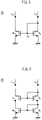
- Fig. 4 is a circuit diagram illustrating the infrared detecting device according to Embodiment 1.
- the infrared sensing portion 8 includes the plurality of diodes 11 connected in series.
- the diode 11 has its anode connected to a first power supply V DD .
- a cathode voltage of the diode 11 is outputted as an output voltage V pix of the infrared detecting device 2.
- the positive feedback circuit 18 includes a P-type MOS transistor Mdp and a current mirror circuit 20.
- the P-type MOS transistor Mdp has its gate receiving the cathode voltage of the diode 11.
- the P-type MOS transistor Mdp has its source connected to a second power supply V DS .
- the current mirror circuit 20 receives a drain current of the P-type MOS transistor Mdp. An output of the current mirror circuit 20 is connected to a cathode of the diode 11.
- Figs. 5 and 6 are circuit diagrams each illustrating the current mirror circuit.
- the current mirror circuit 20 illustrated in Fig. 5 includes N-type MOS transistors Mmn and Mcn.
- the N-type MOS transistor Mmn has its drain and gate connected to each other, and is connected to a gate of the N-type MOS transistor Mcn.
- the N-type MOS transistors Mmn and Mcn have their respective sources grounded.
- the current mirror circuit 20 illustrated in Fig. 6 includes N-type MOS transistors Mmm, Mcn, Mmn', and Mcn'.
- the N-type MOS transistor Mmn has its drain and gate connected to each other, and is connected to a gate of the N-type MOS transistor Mcn.
- the N-type MOS transistors Mmn and Mcn have their respective sources grounded.
- the N-type MOS transistor Mmn' has its drain and gate connected to each other, and is connected to a gate of the N-type MOS transistor Mcn'.
- the N-type MOS transistors Mmn' and Mcn' have their respective sources connected to the drain of the N-type MOS transistor Mmn and a drain of the N-type MOS transistor Mcn.
- An input current Iin is inputted to the drain of the N-type MOS transistor Mmn', and an output current lout is inputted to a drain of the N-type MOS transistor Mcn'.
- a forward voltage Vf of the plurality of diodes 11 decreases. Therefore, a gate voltage of the P-type MOS transistor Mdp as a voltage obtained by subtracting a voltage Vf from a voltage of the power supply V DD increases, and a current Id of the P-type MOS transistor Mdp decreases.
- the current mirror circuit 20 decreases a current If of the diode 11 according to the decrease in the current. As a result, the forward voltage Vf further decreases.
- the forward voltage Vf of the plurality of diodes 11 increases. Therefore, a gate voltage of the P-type MOS transistor Mdp decreases, and the current Id of the P-type MOS transistor Mdp increases.
- the current mirror circuit 20 increases the current If of the diodes 11 according to the increase in the current. As a result, the forward voltage Vf of the diodes 11 further increases. Therefore, respective changes of the forward voltage Vf and the current If of the diodes 11 are subjected to a positive feedback loop.
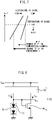
- Fig. 7 is a diagram illustrating a voltage-current characteristic of the diodes in the infrared detecting device according to Embodiment 1.
- An infrared detecting device in a comparative example does not have the positive feedback circuit 18 in the infrared detecting device in Embodiment 1 and is configured such that diodes 11 are subjected to constant current driving by a current source.
- a voltage Vf of the diodes when a temperature of the diodes 11 rises, a voltage Vf of the diodes only decreases.
- the forward voltage Vf of the diodes 11 decreases.
- a gate voltage of the P-type MOS transistor Mdp as a voltage obtained by subtracting the voltage Vf from the voltage of the power supply V DD increases, and the current Id of the P-type MOS transistor Mdp decreases.
- a current mirror circuit 20 decreases the current If of the diodes 11 according to the decrease in the current.
- the forward voltage Vf further decreases. Therefore, a voltage change that is not less than a voltage change obtained from one of the diodes by absolving incident infrared rays in a constant current operation of the diodes in the comparative example is obtained.
- the detection sensitivity of the infrared detecting device can be increased without increasing the number of the diodes.
- Z be an impedance of the diode 11
- gmd be a mutual conductance of the P-type MOS transistor Mdp
- ⁇ be a current mirror current ratio (output/input)
- Fig. 8 is a circuit diagram illustrating an infrared detecting device according to Embodiment 2.
- a plurality of diodes 11 have their respective cathodes grounded.
- An anode voltage of the diode 11 is outputted as an output voltage V pix of a thermal-type infrared detecting device.
- a positive feedback circuit 18 includes an N-type MOS transistor Mdn and a current mirror circuit 20.
- the N-type MOS transistor Mdn has its gate receiving the anode voltage of the diode 11.
- the N-type MOS transistor Mdn has its source grounded.
- the current mirror circuit 20 receives a drain current of the N-type MOS transistor Mdn. An output of the current mirror circuit 20 is connected to an anode of the diode 11.
- Figs. 9 and 10 are circuit diagrams each illustrating the current mirror circuit.
- the current mirror circuit 20 illustrated in Fig. 9 includes P-type MOS transistors Mmp and Mcp.
- the P-type MOS transistor Mmp has its drain and gate connected to each other, and is connected to a gate of the P-type MOS transistor Mcp.
- the P-type MOS transistors Mmp and Mcp have their respective sources connected to a power supply V DD .
- the current mirror circuit 20 illustrated in Fig. 10 includes P-type MOS transistors Mmp, Mcp, Mmp', and Mcp'.
- the P-type MOS transistor Mmp has its drain and gate connected to each other, and is connected to a gate of the P-type MOS transistor Mcp.
- the P-type MOS transistors Mmp and Mcp have their respective sources connected to a power supply V DD .
- the P-type MOS transistor Mmp' has its drain and gate connected to each other, and is connected to a gate of the P-type MOS transistor Mcp'.
- the P-type MOS transistors Mmp' and Mcp' have their respective sources connected to the drain of the P-type MOS transistor Mmp and a drain of the P-type MOS transistor Mcp.
- An input current lip is drawn from the drain of the P-type MOS transistor Mmp', and an output current lout is drawn from a drain of the P-type MOS transistor Mcp'.
- the infrared detecting device having such a configuration, when a temperature of the plurality of diodes 11 rises, a forward voltage Vf of the plurality of diodes 11 decreases. Therefore, a gate voltage of the N-type MOS transistor Mdn decreases, and a current Id of the N-type MOS transistor Mdn decreases.
- the current mirror circuit 20 decreases a current If of the diodes 11 according to the decrease in the current. As a result, the voltage Vf further decreases.
- the forward voltage Vf of the plurality of diodes 11 increases. Therefore, a gate voltage of the N-type MOS transistor Mdn increase, and the current Id of the N-type MOS transistor Mdn increases.
- the current mirror circuit 20 increases the current If of the diodes 11 according to the increase in the current. As a result, the forward voltage Vf of the diodes 11 further increases.
- Z be an impedance of the diode 11
- gmd be a mutual conductance of the N-type MOS transistor Mdn
- ⁇ be a current mirror current ratio (output/input)
- Fig. 11 is a circuit diagram illustrating an infrared detecting device according to Embodiment 3.
- a resistor R pix is connected between a cathode of a diode 11 and an output of a current mirror circuit 20.
- a diode voltage Vf decreases.
- a current If of the diode 11 decreases by a positive feedback loop, and the diode voltage Vf further decreases.
- an output voltage V pix of the infrared detecting device is determined by the diode voltage Vf and a voltage drop amount in the resistor R pix by the current If of the diode 11.
- the resistor R pix If the current If of the diode 11 is on the order of several microamperes, a resistor having a high resistance of about several kiloohms is used as the resistor R pix . As a result, the voltage drop amount in the resistor R pix by the current If of the diode 11 can be increased.
- Fig. 12 is a circuit diagram illustrating a modification of the infrared detecting device according to Embodiment 3.
- a resistor R pix is connected between an anode of a diode 11 and a current mirror circuit 20.
- an infrared detecting device having a high sensitivity can be implemented.
- Other components and effects are similar to those in Embodiment 2.
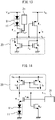
- Fig. 13 is a circuit diagram illustrating an infrared detecting device according to Embodiment 4.
- the resistor R pix in Embodiment 3 illustrated in Fig. 11 is composed of an N-type MOS transistor. Even when not only when a temperature rise occurs by incident infrared rays but also when an environmental temperature as a temperature around the infrared detecting device when using the infrared detecting device increases, a current If of a diode 11 decreases so that a gain changes.
- a control circuit 21 changes a gate voltage V AMB of the N-type MOS transistor composing the resistor R pix according to the environmental temperature. The higher the environmental temperature becomes, the smaller a resistance value of the resistor R pix is made.
- the N-type MOS transistor is used in an operation range of a linear region relative to the change in the environmental temperature.
- Other components and effects are similar to those in Embodiment 3.
- Fig. 14 is a circuit diagram illustrating a modification of the infrared detecting device according to Embodiment 4.
- the resistor R pix in the modification of Embodiment 3 illustrated in Fig. 12 is composed of an N-type MOS transistor.
- a control circuit 21 changes a gate voltage V AMB of the N-type MOS transistor according to an environmental temperature. The higher the environmental temperature becomes, the smaller a resistance value of the resistor R pix is made. As a result, a change in gain due to a change in the environmental temperature can be reduced.
- Other components and effects are similar to those in Embodiment 3.
- Fig. 15 is a circuit diagram illustrating an infrared detecting device according to Embodiment 5.
- An anode of a diode 11 and a source of a P-type MOS transistor Mdp are connected to the same power supply V DD .
- an anode voltage of the diode 11 and a source voltage of the P-type MOS transistor Mdp are the same.
- the sensitivity of the infrared detecting device does not change when a power supply voltage varies. There is no change in gain due to the variation in the power supply voltage.
- Other components and effects are similar to those in Embodiment 3.
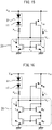
- FIG. 16 is a circuit diagram illustrating an infrared detecting device according to Embodiment 6.
- a current mirror circuit 20 includes cascode-connected N-type MOS transistors Mmn, Mcn, Mmn', and Mcn'.
- the N-type MOS transistor Mmn has its drain and gate connected to each other, and is connected to a gate of the N-type MOS transistor Mcn.
- the N-type MOS transistors Mmn and Mcn have their respective sources grounded.
- the N-type MOS transistor Mmn' has its drain and gate connected to each other, and is connected to a gate of the N-type MOS transistor Mcn'.
- the N-type MOS transistors Mmn' and Mcn' have their respective sources connected to the drain of the N-type MOS transistor Mmn and a drain of the N-type MOS transistor Mcn.
- the drain of the N-type MOS transistor Mmn' is connected to a drain of a P-type MOS transistor Mdp, and the N-type MOS transistor Mcn' has its drain connected to a resistor R pix .
- respective drain voltages of the N-type MOS transistor Mmn and the N-type MOS transistor Mcn in the current mirror circuit 20 match each other, and the replication accuracy of a current in the current mirror circuit 20 is improved.
- Other components and effects are similar to those in Embodiment 3.
- FIG. 17 is a circuit diagram illustrating a modification of the infrared detecting device according to Embodiment 6.
- a current mirror circuit 20 includes cascode-connected P-type MOS transistors Mmp, Mcp, Mmp', and Mcp'.
- the P-type MOS transistor Mmp has its drain and gate connected to each other, and is connected to a gate of the P-type MOS transistor Mcp.
- the P-type MOS transistors Mmp and Mcp have their respective sources connected to a power supply V DD .
- the P-type MOS transistor Mmp' has its drain and gate connected to each other, and is connected to a gate of the P-type MOS transistor Mcp'.
- the P-type MOS transistors Mmp' and Mcp' have their respective sources connected to the drain of the P-type MOS transistor Mmp and a drain of the P-type MOS transistor Mcp.
- the drain of the P-type MOS transistor Mmp' is connected to a drain of an N-type MOS transistor Mdn, and the P-type MOS transistor Mcp' has its drain connected to a resistor R pix .
- respective drain voltages of the P-type MOS transistor Mmp and the P-type MOS transistor Mcp in the current mirror circuit 20 match each other, and the replication accuracy of a current in the current mirror circuit 20 is improved.
- Other components and effects are similar to those in Embodiment 4.
- Fig. 18 is a circuit diagram illustrating an infrared detecting device according to Embodiment 7.
- a current mirror circuit 20 includes N-type MOS transistors Mmn and Mcn.
- the N-type MOS transistor Mmn has its drain and gate connected to each other, and is connected to a gate of the N-type MOS transistor Mcn.
- the N-type MOS transistors Mmn and Mcn have their respective sources grounded.
- the drain of the N-type MOS transistor Mmn is connected to a drain of a P-type MOS transistor Mdp, and the N-type MOS transistor Mcn has its drain connected to an infrared sensing portion 8.
- An N-type MOS transistor Msu is diode-connected between a cathode of a diode 11 and the gate of the N-type MOS transistors Mmn and a gate of the N-type MOS transistor Mcn in a current source of the current mirror circuit 20.
- the N-type MOS transistor Msu has its gate and drain connected to the cathode of the diode 11, and the N-type MOS transistor Msu has its source connected to the respective gates of the N-type MOS transistors Mmn and Mcn.
- a threshold voltage of the MOS transistor Msu is set lower than a voltage of a power supply V DD to be applied to an anode of the diode 11, and is set higher than a normal operation voltage range as a voltage range between an upper limit value and a lower limit value of a cathode voltage V pix of the diode 11 that changes by incidence of infrared rays from an object in a subject temperature range (from a lower limit temperature to an upper limit temperature) as a detection target of the infrared detecting device.
- Other components are similar to those in Embodiment 1.
- the MOS transistor Msu is turned on at the time of defective startup.
- the voltage V pix is forcedly reduced, a current is made to flow through the MOS transistors Mdp, Mmn, and Mcn in this order so that the infrared detecting device can be reliably started up.
- a similar effect to that in Embodiment 1 can be obtained.
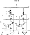
- Fig. 19 is a circuit diagram illustrating an infrared detecting device according to Embodiment 8.
- a plurality of infrared sensing portions 8 are arranged in an array shape.
- a positive feedback circuit 18, a current source 22, and a differential integration circuit 23 are provided for each column including each of a plurality of infrared sensing portions 8 arranged in an array shape.
- Each of the infrared sensing portions 8 includes a plurality of diodes 11 connected in series. Therefore, the positive feedback circuit 18 is provided for each column of the plurality of diodes 11 connected in series.
- MOS transistors Mmn and Mcn in the current mirror circuit 20 have the same specification, and a current mirror ratio ⁇ of the current mirror circuit 20 is 1.
- the diodes 11 in the plurality of infrared sensing portions 8 have their respective anodes sequentially connected to a driving line 24 in an arrangement direction of the plurality of infrared sensing portions 8.
- One end of the driving line 24 is connected to a power supply V DD .
- P-type MOS transistors Mdp in the plurality of positive feedback circuits 18 have their respective sources sequentially connected to a circuit power supply line 25 in the arrangement direction of the plurality of infrared sensing portions 8.
- One end of the circuit power supply line 25 is connected to a power supply V DS .
- the plurality of current sources 22 are sequentially connected to a dummy driving line 26 in the arrangement direction of the plurality of infrared sensing portions 8.
- the circuit power supply line 25, the driving line 24, and the dummy driving line 26 have the same resistance.
- the current source 22 includes a MOS transistor Mcd having the same specification as that of the MOS transistors Mmn and Mcn in the corresponding current mirror circuit 20. Respective gates of the MOS transistors Mmn and Mcn in the corresponding current mirror circuit 20 and a gate of the N-type MOS transistor Mcd in the current source 22 are commonly connected.
- the N-type MOS transistor Mcd has its source grounded, and the N-type MOS transistor Mcd has its drain connected to the dummy driving line 26.
- a current value of the current source 22 is set such that a potential distribution of the dummy driving line 26 and a potential distribution of the driving line 24 in the arrangement direction of the plurality of infrared sensing portions 8 are the same. Therefore, a voltage drop of the driving line 24 is simulated on the dummy driving line 26.
- a connection point between the diode 11 in the infrared sensing portion 8 and the driving line 24 and a connection point between the corresponding current source 22 and the dummy driving line 26 are at the same position in the arrangement direction of the plurality of infrared sensing portions 8.
- the differential integration circuit 23 amplifies a difference between an output voltage of the corresponding current mirror circuit 20 and a voltage of the connection point between the corresponding current source 22 and the dummy driving line 26 and outputs the difference.
- Fig. 20 is a circuit diagram illustrating an infrared detecting device according to Embodiment 9.
- a signal line 27 connects a cathode of a diode 11 to a corresponding differential integration circuit 23.
- a switch SW1 is connected between a power supply V DD that supplies a voltage to the diode 11 and an anode of the diode 11.
- a switch SW2 for startup is connected between a dummy driving line 26 and the signal line 27. Specifically, one end of the switch SW2 is connected to the signal line 27, and the other end of the switch SW2 is connected to the differential integration circuit 23, a drain of an N-type MOS transistor Mcd, and the dummy driving line 26.
- the switch SW2 short-circuits the signal line 27 and the dummy driving line 26 in a horizontal blanking period, and a gate voltage of a P-type MOS transistor Mdp is forcedly reduced to make a current flow.
- the infrared detecting device can be normally started up.
- the switch SW2 is operated at a timing reverse to that of the switch SW1.
Landscapes
- Physics & Mathematics (AREA)
- General Physics & Mathematics (AREA)
- Spectroscopy & Molecular Physics (AREA)
- Chemical & Material Sciences (AREA)
- Crystallography & Structural Chemistry (AREA)
- Photometry And Measurement Of Optical Pulse Characteristics (AREA)
- Solid State Image Pick-Up Elements (AREA)
Abstract
Description
- The present disclosure relates to an infrared detecting device that converts infrared rays into heat and detects it.
- Infrared detecting devices are roughly classified into quantum type infrared detecting devices and thermal type infrared detecting devices. The quantum type infrared detecting device is a cooled type infrared detecting device requiring a cooling machine. On the other hand, the thermal type infrared detecting device is an uncooled type infrared detecting device not requiring a cooling machine and can be therefore miniaturized. The thermal type infrared detecting device is a detecting device that converts infrared rays absorbed by an infrared absorber into heat and converts a temperature change caused by the heat into an electric signal.
- In recent years, cost reduction aiming at consumer applications of the infrared detecting device has progressed and a sensing capability has been improved. If a diode is used as a temperature sensor in the infrared detecting device, the detection sensitivity of the infrared detecting device is enhanced by connecting a plurality of diodes in series because a temperature change rate of each of the diodes is small.
- As many diodes as possible have been required to be connected in series and arranged in the limited area of a temperature sensing portion in an infrared detecting device. On the other hand, an infrared detecting device in which adjacent first and second diodes are connected to each other by a metal film provided on a surface of a recess formed to span a p-type layer of the first diode and an N-type layer of the second diode has been proposed (see, e.g., PTL 1). As a result, a spacing between the adjacent diodes is smaller than that when the diodes are separated from each other through an oxide film. Therefore, the plurality of diodes can be formed at a high density. Thus, the detection sensitivity of the infrared detecting device can be enhanced.
- [PTL 1]
JP 2009-265094 A - In the conventional infrared detecting device, the number of the plurality of diodes connected in series in the temperature sensing portion needs to be increased to enhance the detection sensitivity. The increase in the number of the diodes leads to an increase in size of the infrared detecting device, and requires a high power supply voltage.
- The present disclosure has been made to solve the above-described problem, and is directed to obtaining an infrared detecting device the detection sensitivity of which can be enhanced without increasing the number of diodes.
- An infrared detecting device according to the present disclosure includes: a substrate; a diode provided on the substrate and thermally insulated from the substrate; and a positive feedback circuit providing a positive feedback loop so that when a current of the diode decreases due to a change in temperature of the diode, the positive feedback circuit further decreases the current of the diode, and when the current of the diode increases, the positive feedback circuit further increases the current of the diode.
- The infrared detecting device of the present disclosure configured as described above can increase the detection sensitivity without increasing the number of the diodes.
-
-
Fig. 1 is a perspective view illustrating an infrared imaging apparatus according toEmbodiment 1. -
Fig. 2 is a top view illustrating the infrared detecting device according toEmbodiment 1. -
Fig. 3 is a cross-sectional view taken along a line I - II illustrated inFig. 1 . -
Fig. 4 is a circuit diagram illustrating the infrared detecting device according toEmbodiment 1. -
Fig. 5 is a circuit diagram illustrating the current mirror circuit. -
Fig. 6 is a circuit diagram illustrating the current mirror circuit. -
Fig. 7 is a diagram illustrating a voltage-current characteristic of the diodes in the infrared detecting device according toEmbodiment 1. -
Fig. 8 is a circuit diagram illustrating an infrared detecting device according toEmbodiment 2. -
Fig. 9 is a circuit diagram illustrating the current mirror circuit. -
Fig. 10 is a circuit diagram illustrating the current mirror circuit. -
Fig. 11 is a circuit diagram illustrating an infrared detecting device according to Embodiment 3. -
Fig. 12 is a circuit diagram illustrating a modification of the infrared detecting device according to Embodiment 3. -
Fig. 13 is a circuit diagram illustrating an infrared detecting device according toEmbodiment 4. -
Fig. 14 is a circuit diagram illustrating a modification of the infrared detecting device according toEmbodiment 4. -
Fig. 15 is a circuit diagram illustrating an infrared detecting device according toEmbodiment 5. -
Fig. 16 is a circuit diagram illustrating an infrared detecting device according toEmbodiment 6. -
Fig. 17 is a circuit diagram illustrating a modification of the infrared detecting device according toEmbodiment 6. -
Fig. 18 is a circuit diagram illustrating an infrared detecting device according to Embodiment 7. -
Fig. 19 is a circuit diagram illustrating an infrared detecting device according toEmbodiment 8. -
Fig. 20 is a circuit diagram illustrating an infrared detecting device according toEmbodiment 9. - An infrared detecting device according to the embodiments of the present disclosure will be described with reference to the drawings. The same components will be denoted by the same symbols, and the repeated description thereof may be omitted.
-
Fig. 1 is a perspective view illustrating an infrared imaging apparatus according toEmbodiment 1. A plurality of infrared detectingdevices 2 are two-dimensionally arranged in an array shape or a matrix shape on asubstrate 1. Selection lines 3 andsignal lines 4 are provided along the plurality of infrared detectingdevices 2. The selection lines 3 are connected to adrive scanning circuit 5. Thesignal lines 4 are connected to asignal scanning circuit 6. Thedrive scanning circuit 5 and thesignal scanning circuit 6 are provided around the plurality of infrared detectingdevices 2. An output signal of theinfrared detecting device 2 selected by thedrive scanning circuit 5 and thesignal scanning circuit 6 is amplified by an output amplifier 7 composed of an integration circuit. -
Fig. 2 is a top view illustrating the infrared detecting device according toEmbodiment 1. Theinfrared detecting device 2 has an insulation structure formed using a micro-machining technique. Aninfrared sensing portion 8 is formed on the insulation structure. Theinfrared sensing portion 8 is thermally insulated from thesubstrate 1 by the insulation structure. Theinfrared sensing portion 8 rises in temperature when infrared rays are incident thereon. The temperature rise is detected by theinfrared sensing portion 8, and is outputted as an electric signal. Respective output signals of the plurality of infrared detectingdevices 2 are read out in time series using a scanning operation of thedrive scanning circuit 5 and thesignal scanning circuit 6, to obtain an infrared image signal. -
Fig. 3 is a cross-sectional view taken along a line I - II illustrated inFig. 1 . Theinfrared detecting device 2 includes an infrared sensing region and a circuit region. Thesubstrate 1 is an SOI (silicon on insulator) substrate, for example. In the infrared sensing region, thesubstrate 1 is provided with acavity 9. Theinfrared sensing portion 8 is arranged in thecavity 9 with it being spaced apart from thesubstrate 1, and is supported by asupport leg 10. Thecavity 9 has the above-described insulation structure. - The
infrared sensing portion 8 is a pixel including a plurality ofdiodes 11 connected in series as a temperature sensor. Examples of thediode 11 include a Schottky diode and a tunnel diode. Instead of thediode 11, there is provided another thermoelectric conversion device having an electrical characteristic changing depending on a temperature. Athin film wiring 13, aninterlayer insulating film 14, and aprotective film 15 are sequentially provided on an insulatingfilm 12 that covers thediode 11. Thethin film wiring 13 is connected to thediode 11. An infrared absorbingportion 16 having an umbrella structure for absorbing infrared rays is provided on theprotective film 15. - The
support leg 10 has a laminate structure of the insulatingfilm 12, aninterlayer insulating film 17, thethin film wiring 13, theinterlayer insulating film 14, and theprotective film 15. The insulatingfilm 12, theinterlayer insulating film 17, theinterlayer insulating film 14, and theprotective film 15 are each composed of silicon oxide or silicon nitride, for example. Thethin film wiring 13 is composed of a metal such as aluminum, Ti, TiN, Ni, Cr, or Pt or polycrystalline silicon. - In the circuit region, a
positive feedback circuit 18 and awiring 19 connected to thepositive feedback circuit 18 are provided. Thepositive feedback circuit 18 includes a scanning circuit, a current source circuit, a power supply circuit, an integration circuit, or a MOS (metal oxide semiconductor) transistor. - In the infrared detecting
device 2, the incident infrared rays are converted into heat upon being absorbed by the infrared absorbingportion 16, and the heat is conducted to theinfrared sensing portion 8. When the temperature of theinfrared sensing portion 8 rises, an electrical characteristic of thediode 11 included in theinfrared sensing portion 8 changes. Thethin film wiring 13 connected to each of the p-side and the n-side of thediode 11 is connected to thewiring 19 through thesupport leg 10. A change in the electrical characteristic of thediode 11 is taken out as an electric signal to thepositive feedback circuit 18 through thethin film wiring 13 and thewiring 19, and is used to detect the incident infrared rays. -
Fig. 4 is a circuit diagram illustrating the infrared detecting device according toEmbodiment 1. Theinfrared sensing portion 8 includes the plurality ofdiodes 11 connected in series. Thediode 11 has its anode connected to a first power supply VDD. A cathode voltage of thediode 11 is outputted as an output voltage Vpix of the infrared detectingdevice 2. - The
positive feedback circuit 18 includes a P-type MOS transistor Mdp and acurrent mirror circuit 20. The P-type MOS transistor Mdp has its gate receiving the cathode voltage of thediode 11. The P-type MOS transistor Mdp has its source connected to a second power supply VDS. - The
current mirror circuit 20 receives a drain current of the P-type MOS transistor Mdp. An output of thecurrent mirror circuit 20 is connected to a cathode of thediode 11.Figs. 5 and 6 are circuit diagrams each illustrating the current mirror circuit. Thecurrent mirror circuit 20 illustrated inFig. 5 includes N-type MOS transistors Mmn and Mcn. The N-type MOS transistor Mmn has its drain and gate connected to each other, and is connected to a gate of the N-type MOS transistor Mcn. The N-type MOS transistors Mmn and Mcn have their respective sources grounded. An input current Iin is inputted to the drain of the N-type MOS transistor Mmn, and an output current lout is inputted to a drain of the N-type MOS transistor Mcn. Thecurrent mirror circuit 20 illustrated inFig. 6 includes N-type MOS transistors Mmm, Mcn, Mmn', and Mcn'. The N-type MOS transistor Mmn has its drain and gate connected to each other, and is connected to a gate of the N-type MOS transistor Mcn. The N-type MOS transistors Mmn and Mcn have their respective sources grounded. The N-type MOS transistor Mmn' has its drain and gate connected to each other, and is connected to a gate of the N-type MOS transistor Mcn'. The N-type MOS transistors Mmn' and Mcn' have their respective sources connected to the drain of the N-type MOS transistor Mmn and a drain of the N-type MOS transistor Mcn. An input current Iin is inputted to the drain of the N-type MOS transistor Mmn', and an output current lout is inputted to a drain of the N-type MOS transistor Mcn'. - In the infrared detecting device having such a configuration, when a temperature of the plurality of
diodes 11 rises, a forward voltage Vf of the plurality ofdiodes 11 decreases. Therefore, a gate voltage of the P-type MOS transistor Mdp as a voltage obtained by subtracting a voltage Vf from a voltage of the power supply VDD increases, and a current Id of the P-type MOS transistor Mdp decreases. Thecurrent mirror circuit 20 decreases a current If of thediode 11 according to the decrease in the current. As a result, the forward voltage Vf further decreases. - When the temperature of the
diodes 11 drops, the forward voltage Vf of the plurality ofdiodes 11 increases. Therefore, a gate voltage of the P-type MOS transistor Mdp decreases, and the current Id of the P-type MOS transistor Mdp increases. Thecurrent mirror circuit 20 increases the current If of thediodes 11 according to the increase in the current. As a result, the forward voltage Vf of thediodes 11 further increases. Therefore, respective changes of the forward voltage Vf and the current If of thediodes 11 are subjected to a positive feedback loop. -
Fig. 7 is a diagram illustrating a voltage-current characteristic of the diodes in the infrared detecting device according toEmbodiment 1. An infrared detecting device in a comparative example does not have thepositive feedback circuit 18 in the infrared detecting device inEmbodiment 1 and is configured such thatdiodes 11 are subjected to constant current driving by a current source. In the comparative example, when a temperature of thediodes 11 rises, a voltage Vf of the diodes only decreases. In the present embodiment, when the temperature of thediodes 11 as a temperature sensor rises by incident infrared rays, the forward voltage Vf of thediodes 11 decreases. Therefore, a gate voltage of the P-type MOS transistor Mdp as a voltage obtained by subtracting the voltage Vf from the voltage of the power supply VDD increases, and the current Id of the P-type MOS transistor Mdp decreases. Acurrent mirror circuit 20 decreases the current If of thediodes 11 according to the decrease in the current. As a result, the forward voltage Vf further decreases. Therefore, a voltage change that is not less than a voltage change obtained from one of the diodes by absolving incident infrared rays in a constant current operation of the diodes in the comparative example is obtained. As a result, the detection sensitivity of the infrared detecting device can be increased without increasing the number of the diodes. - To stabilize a circuit operation, letting Z be an impedance of the
diode 11, gmd be a mutual conductance of the P-type MOS transistor Mdp, and κ be a current mirror current ratio (output/input), a relationship of 0 < κ · gmd · Z < 1 is preferably satisfied. -
Fig. 8 is a circuit diagram illustrating an infrared detecting device according toEmbodiment 2. A plurality ofdiodes 11 have their respective cathodes grounded. An anode voltage of thediode 11 is outputted as an output voltage Vpix of a thermal-type infrared detecting device. - A
positive feedback circuit 18 includes an N-type MOS transistor Mdn and acurrent mirror circuit 20. The N-type MOS transistor Mdn has its gate receiving the anode voltage of thediode 11. The N-type MOS transistor Mdn has its source grounded. - The
current mirror circuit 20 receives a drain current of the N-type MOS transistor Mdn. An output of thecurrent mirror circuit 20 is connected to an anode of thediode 11.Figs. 9 and 10 are circuit diagrams each illustrating the current mirror circuit. Thecurrent mirror circuit 20 illustrated inFig. 9 includes P-type MOS transistors Mmp and Mcp. The P-type MOS transistor Mmp has its drain and gate connected to each other, and is connected to a gate of the P-type MOS transistor Mcp. The P-type MOS transistors Mmp and Mcp have their respective sources connected to a power supply VDD. An input current lip is drawn from the drain of the P-type MOS transistor Mmp, and an output current lout is drawn from a drain of the P-type MOS transistor Mcp. Thecurrent mirror circuit 20 illustrated inFig. 10 includes P-type MOS transistors Mmp, Mcp, Mmp', and Mcp'. The P-type MOS transistor Mmp has its drain and gate connected to each other, and is connected to a gate of the P-type MOS transistor Mcp. The P-type MOS transistors Mmp and Mcp have their respective sources connected to a power supply VDD. The P-type MOS transistor Mmp' has its drain and gate connected to each other, and is connected to a gate of the P-type MOS transistor Mcp'. The P-type MOS transistors Mmp' and Mcp' have their respective sources connected to the drain of the P-type MOS transistor Mmp and a drain of the P-type MOS transistor Mcp. An input current lip is drawn from the drain of the P-type MOS transistor Mmp', and an output current lout is drawn from a drain of the P-type MOS transistor Mcp'. - In the infrared detecting device having such a configuration, when a temperature of the plurality of
diodes 11 rises, a forward voltage Vf of the plurality ofdiodes 11 decreases. Therefore, a gate voltage of the N-type MOS transistor Mdn decreases, and a current Id of the N-type MOS transistor Mdn decreases. Thecurrent mirror circuit 20 decreases a current If of thediodes 11 according to the decrease in the current. As a result, the voltage Vf further decreases. - When the temperature of the
diodes 11 drops, the forward voltage Vf of the plurality ofdiodes 11 increases. Therefore, a gate voltage of the N-type MOS transistor Mdn increase, and the current Id of the N-type MOS transistor Mdn increases. Thecurrent mirror circuit 20 increases the current If of thediodes 11 according to the increase in the current. As a result, the forward voltage Vf of thediodes 11 further increases. - Therefore, respective changes in the forward voltage Vf and the current If of the
diodes 11 are subjected to a positive feedback loop. Therefore, a voltage change that is not less than a voltage change obtained from one of the diodes by absolving incident infrared rays in a constant current operation of the diodes in the comparative example is obtained, as described inEmbodiment 1 with reference toFig. 7 . As a result, the detection sensitivity of the infrared detecting device can be increased without increasing the number of the diodes. - To stabilize a circuit operation, letting Z be an impedance of the
diode 11, gmd be a mutual conductance of the N-type MOS transistor Mdn, and κ be a current mirror current ratio (output/input), a relationship of 0 < κ · gmd · Z < 1 is preferably satisfied. -
Fig. 11 is a circuit diagram illustrating an infrared detecting device according to Embodiment 3. A resistor Rpix is connected between a cathode of adiode 11 and an output of acurrent mirror circuit 20. When a temperature of thediode 11 rises, a diode voltage Vf decreases. A current If of thediode 11 decreases by a positive feedback loop, and the diode voltage Vf further decreases. At this time, an output voltage Vpix of the infrared detecting device is determined by the diode voltage Vf and a voltage drop amount in the resistor Rpix by the current If of thediode 11. When the current If of thediode 11 decreases, the voltage drop amount in the resistor Rpix also decreases. Thus, a change in the output voltage Vpix of the infrared detecting device further increases. As a result, an infrared detecting device having a high sensitivity can be implemented. Other components and effects are similar to those inEmbodiment 1. - If the current If of the
diode 11 is on the order of several microamperes, a resistor having a high resistance of about several kiloohms is used as the resistor Rpix. As a result, the voltage drop amount in the resistor Rpix by the current If of thediode 11 can be increased. -
Fig. 12 is a circuit diagram illustrating a modification of the infrared detecting device according to Embodiment 3. A resistor Rpix is connected between an anode of adiode 11 and acurrent mirror circuit 20. As a result, an infrared detecting device having a high sensitivity can be implemented. Other components and effects are similar to those inEmbodiment 2. -
Fig. 13 is a circuit diagram illustrating an infrared detecting device according toEmbodiment 4. The resistor Rpix in Embodiment 3 illustrated inFig. 11 is composed of an N-type MOS transistor. Even when not only when a temperature rise occurs by incident infrared rays but also when an environmental temperature as a temperature around the infrared detecting device when using the infrared detecting device increases, a current If of adiode 11 decreases so that a gain changes. Acontrol circuit 21 changes a gate voltage VAMB of the N-type MOS transistor composing the resistor Rpix according to the environmental temperature. The higher the environmental temperature becomes, the smaller a resistance value of the resistor Rpix is made. As a result, the change in the gain due to a change in the environmental temperature can be reduced. The N-type MOS transistor is used in an operation range of a linear region relative to the change in the environmental temperature. Other components and effects are similar to those in Embodiment 3. -
Fig. 14 is a circuit diagram illustrating a modification of the infrared detecting device according toEmbodiment 4. The resistor Rpix in the modification of Embodiment 3 illustrated inFig. 12 is composed of an N-type MOS transistor. Acontrol circuit 21 changes a gate voltage VAMB of the N-type MOS transistor according to an environmental temperature. The higher the environmental temperature becomes, the smaller a resistance value of the resistor Rpix is made. As a result, a change in gain due to a change in the environmental temperature can be reduced. Other components and effects are similar to those in Embodiment 3. -
Fig. 15 is a circuit diagram illustrating an infrared detecting device according toEmbodiment 5. An anode of adiode 11 and a source of a P-type MOS transistor Mdp are connected to the same power supply VDD. As a result, an anode voltage of thediode 11 and a source voltage of the P-type MOS transistor Mdp are the same. Thus, the sensitivity of the infrared detecting device does not change when a power supply voltage varies. There is no change in gain due to the variation in the power supply voltage. Other components and effects are similar to those in Embodiment 3. -
Fig. 16 is a circuit diagram illustrating an infrared detecting device according toEmbodiment 6. Acurrent mirror circuit 20 includes cascode-connected N-type MOS transistors Mmn, Mcn, Mmn', and Mcn'. The N-type MOS transistor Mmn has its drain and gate connected to each other, and is connected to a gate of the N-type MOS transistor Mcn. The N-type MOS transistors Mmn and Mcn have their respective sources grounded. The N-type MOS transistor Mmn' has its drain and gate connected to each other, and is connected to a gate of the N-type MOS transistor Mcn'. The N-type MOS transistors Mmn' and Mcn' have their respective sources connected to the drain of the N-type MOS transistor Mmn and a drain of the N-type MOS transistor Mcn. The drain of the N-type MOS transistor Mmn' is connected to a drain of a P-type MOS transistor Mdp, and the N-type MOS transistor Mcn' has its drain connected to a resistor Rpix. As a result, respective drain voltages of the N-type MOS transistor Mmn and the N-type MOS transistor Mcn in thecurrent mirror circuit 20 match each other, and the replication accuracy of a current in thecurrent mirror circuit 20 is improved. Other components and effects are similar to those in Embodiment 3. -
Fig. 17 is a circuit diagram illustrating a modification of the infrared detecting device according toEmbodiment 6. Acurrent mirror circuit 20 includes cascode-connected P-type MOS transistors Mmp, Mcp, Mmp', and Mcp'. The P-type MOS transistor Mmp has its drain and gate connected to each other, and is connected to a gate of the P-type MOS transistor Mcp. The P-type MOS transistors Mmp and Mcp have their respective sources connected to a power supply VDD. The P-type MOS transistor Mmp' has its drain and gate connected to each other, and is connected to a gate of the P-type MOS transistor Mcp'. The P-type MOS transistors Mmp' and Mcp' have their respective sources connected to the drain of the P-type MOS transistor Mmp and a drain of the P-type MOS transistor Mcp. The drain of the P-type MOS transistor Mmp' is connected to a drain of an N-type MOS transistor Mdn, and the P-type MOS transistor Mcp' has its drain connected to a resistor Rpix. As a result, respective drain voltages of the P-type MOS transistor Mmp and the P-type MOS transistor Mcp in thecurrent mirror circuit 20 match each other, and the replication accuracy of a current in thecurrent mirror circuit 20 is improved. Other components and effects are similar to those inEmbodiment 4. -
Fig. 18 is a circuit diagram illustrating an infrared detecting device according to Embodiment 7. Acurrent mirror circuit 20 includes N-type MOS transistors Mmn and Mcn. The N-type MOS transistor Mmn has its drain and gate connected to each other, and is connected to a gate of the N-type MOS transistor Mcn. The N-type MOS transistors Mmn and Mcn have their respective sources grounded. The drain of the N-type MOS transistor Mmn is connected to a drain of a P-type MOS transistor Mdp, and the N-type MOS transistor Mcn has its drain connected to aninfrared sensing portion 8. An N-type MOS transistor Msu is diode-connected between a cathode of adiode 11 and the gate of the N-type MOS transistors Mmn and a gate of the N-type MOS transistor Mcn in a current source of thecurrent mirror circuit 20. The N-type MOS transistor Msu has its gate and drain connected to the cathode of thediode 11, and the N-type MOS transistor Msu has its source connected to the respective gates of the N-type MOS transistors Mmn and Mcn. A threshold voltage of the MOS transistor Msu is set lower than a voltage of a power supply VDD to be applied to an anode of thediode 11, and is set higher than a normal operation voltage range as a voltage range between an upper limit value and a lower limit value of a cathode voltage Vpix of thediode 11 that changes by incidence of infrared rays from an object in a subject temperature range (from a lower limit temperature to an upper limit temperature) as a detection target of the infrared detecting device. Other components are similar to those inEmbodiment 1. - In
Embodiment 1, a stable point exists even when If = 0, Vg = 0, and Vpix = VDD. In the present embodiment, the MOS transistor Msu is turned on at the time of defective startup. When the voltage Vpix is forcedly reduced, a current is made to flow through the MOS transistors Mdp, Mmn, and Mcn in this order so that the infrared detecting device can be reliably started up. In addition, a similar effect to that inEmbodiment 1 can be obtained. -
Fig. 19 is a circuit diagram illustrating an infrared detecting device according toEmbodiment 8. A plurality ofinfrared sensing portions 8 are arranged in an array shape. Apositive feedback circuit 18, acurrent source 22, and adifferential integration circuit 23 are provided for each column including each of a plurality ofinfrared sensing portions 8 arranged in an array shape. Each of theinfrared sensing portions 8 includes a plurality ofdiodes 11 connected in series. Therefore, thepositive feedback circuit 18 is provided for each column of the plurality ofdiodes 11 connected in series. MOS transistors Mmn and Mcn in thecurrent mirror circuit 20 have the same specification, and a current mirror ratio κ of thecurrent mirror circuit 20 is 1. - The
diodes 11 in the plurality ofinfrared sensing portions 8 have their respective anodes sequentially connected to adriving line 24 in an arrangement direction of the plurality ofinfrared sensing portions 8. One end of the drivingline 24 is connected to a power supply VDD. P-type MOS transistors Mdp in the plurality ofpositive feedback circuits 18 have their respective sources sequentially connected to a circuitpower supply line 25 in the arrangement direction of the plurality ofinfrared sensing portions 8. One end of the circuitpower supply line 25 is connected to a power supply VDS. The plurality ofcurrent sources 22 are sequentially connected to adummy driving line 26 in the arrangement direction of the plurality ofinfrared sensing portions 8. - The circuit
power supply line 25, the drivingline 24, and thedummy driving line 26 have the same resistance. Thecurrent source 22 includes a MOS transistor Mcd having the same specification as that of the MOS transistors Mmn and Mcn in the correspondingcurrent mirror circuit 20. Respective gates of the MOS transistors Mmn and Mcn in the correspondingcurrent mirror circuit 20 and a gate of the N-type MOS transistor Mcd in thecurrent source 22 are commonly connected. The N-type MOS transistor Mcd has its source grounded, and the N-type MOS transistor Mcd has its drain connected to thedummy driving line 26. A current value of thecurrent source 22 is set such that a potential distribution of thedummy driving line 26 and a potential distribution of the drivingline 24 in the arrangement direction of the plurality ofinfrared sensing portions 8 are the same. Therefore, a voltage drop of the drivingline 24 is simulated on thedummy driving line 26. - A connection point between the
diode 11 in theinfrared sensing portion 8 and the drivingline 24 and a connection point between the correspondingcurrent source 22 and thedummy driving line 26 are at the same position in the arrangement direction of the plurality ofinfrared sensing portions 8. Thedifferential integration circuit 23 amplifies a difference between an output voltage of the correspondingcurrent mirror circuit 20 and a voltage of the connection point between the correspondingcurrent source 22 and thedummy driving line 26 and outputs the difference. As a result, even if a voltage change of the drivingline 24 occurs due to a current change of thecertain diode 11, an effect on an output of theinfrared sensing portion 8 including theother diode 11 can be eliminated. -
Fig. 20 is a circuit diagram illustrating an infrared detecting device according toEmbodiment 9. Asignal line 27 connects a cathode of adiode 11 to a correspondingdifferential integration circuit 23. A switch SW1 is connected between a power supply VDD that supplies a voltage to thediode 11 and an anode of thediode 11. A switch SW2 for startup is connected between adummy driving line 26 and thesignal line 27. Specifically, one end of the switch SW2 is connected to thesignal line 27, and the other end of the switch SW2 is connected to thedifferential integration circuit 23, a drain of an N-type MOS transistor Mcd, and thedummy driving line 26. - The switch SW2 short-circuits the
signal line 27 and thedummy driving line 26 in a horizontal blanking period, and a gate voltage of a P-type MOS transistor Mdp is forcedly reduced to make a current flow. As a result, the infrared detecting device can be normally started up. For example, the switch SW2 is operated at a timing reverse to that of the switch SW1. - 1 substrate; 8 infrared sensing portion; 11 diode; 18 positive feedback circuit; 20 current mirror circuit; 21 control circuit; 22 current source; 23 differential integration circuit; 24 driving line; 26 dummy driving line; 27 signal line; Mdp,Mmp,Mcp,Mmp',Mcp' P-type MOS transistor; Mdn,Mmn,Mcn,Mmn',Mcn',Msu N-type MOS transistor; Rpix resistor; SW2 switch
Claims (14)
- An infrared detecting device comprising:a substrate;a diode provided on the substrate and thermally insulated from the substrate; anda positive feedback circuit providing a positive feedback loop so that when a current of the diode decreases due to a change in temperature of the diode, the positive feedback circuit further decreases the current of the diode, and when the current of the diode increases, the positive feedback circuit further increases the current of the diode.
- The infrared detecting device according to claim 1, wherein the positive feedback circuit includes a P-type MOS transistor having a gate receiving cathode voltage of the diode, and a current mirror circuit receiving a drain current of the P-type MOS transistor and having an output connected to a cathode of the diode.
- The infrared detecting device according to claim 2, wherein 0< κ · gmd·Z<1 is satisfied, where Z is an impedance of the diode, gmd is a mutual conductance of the P-type MOS transistor, and κ is a current mirror current ratio of the current mirror circuit.
- The infrared detecting device according to claim 1, wherein the positive feedback circuit includes an N-type MOS transistor having a gate receiving anode voltage of the diode, and a current mirror circuit receiving a drain current of the N-type MOS transistor and having an output connected to an anode of the diode.
- The infrared detecting device according to claim 4, wherein 0< κ ·gmd·Z<1 is satisfied, where Z is an impedance of the diode, gmd is a mutual conductance of the N-type MOS transistor, and κ is a current mirror current ratio of the current mirror circuit.
- The infrared detecting device according to any one of claims 2 to 5, further comprising a resistor connected between the diode and an output of the current mirror circuit.
- The infrared detecting device according to claim 6, wherein the resistor is composed of a MOS transistor,the infrared detecting device further comprises a control circuit changes a gate voltage of the MOS transistor according to an environmental temperature as a temperature around the infrared detecting device when using the infrared detecting device, andthe higher the environmental temperature becomes, the smaller a resistance value of the resistor is made by the control circuit.
- The infrared detecting device according to claim 2 or 3, wherein an anode of the diode and a source of the P-type MOS transistor are connected to the same potential.
- The infrared detecting device according to any one of claims 2 to 8, wherein the current mirror circuit includes cascode-connected transistors.
- The infrared detecting device according to claim 2 or 3, further comprising a MOS transistor diode-connected between a cathode of the diode and a gate of a transistor of the current mirror circuit,
wherein a threshold voltage of the MOS transistor is lower than a voltage of a power supply to be applied to an anode of the diode, and is higher than a normal operation voltage range as a voltage range between an upper limit value and a lower limit value of a cathode voltage of the diode that changes by incidence of infrared rays from an object in a subject temperature range as a detection target of the infrared detecting device. - An infrared detecting device comprising:a substrate;a plurality of infrared sensing portions arranged in an array shape on the substrate; andpositive feedback circuits each provided for each column of the plurality of infrared sensing portions arranged in an array shape,wherein each infrared sensing portion includes a plurality of diodes connected in series and thermally insulated from the substrate, andeach positive feedback circuit provides a positive feedback loop so that when a current of the diode of the corresponding infrared sensing portion decreases due to a change in temperature of the diode, the positive feedback circuit further decreases the current of the diode, and when the current of the diode increases, the positive feedback circuit further increases the current of the diode.
- The infrared detecting device according to claim 11, wherein each positive feedback circuit includes a P-type MOS transistor having a gate receiving cathode voltage of the diode of the corresponding infrared sensing portion, and a current mirror circuit receiving a drain current of the P-type MOS transistor and having an output connected to a cathode of the diode,the infrared detecting device further comprises a driving line to which anodes of the diodes in the plurality of infrared sensing portions are sequentially connected in an arrangement direction of the plurality of infrared sensing portions, a plurality of current sources provided for the positive feedback circuits respectively, a dummy driving line to which the plurality of current sources are sequentially connected in the arrangement direction, and a plurality of differential integration circuits provided for the plurality of infrared sensing portions respectively,the driving line and the dummy driving line have the same resistance,current values of the plurality of current sources are set such that a potential distribution of the dummy driving line and a potential distribution of the driving line in the arrangement direction are the same, andthe differential integration circuit outputs a difference between an output voltage of the corresponding current mirror circuit and a voltage of a connection point between the corresponding current source and the dummy driving line.
- The infrared detecting device according to claim 12, wherein the current source includes a MOS transistor having the same specification as that of the MOS transistor in the corresponding current mirror circuit, and
a gate of the MOS transistor in the corresponding current mirror circuit and a gate of the MOS transistor in the current source are commonly connected. - The infrared detecting device according to claim 12 or 13, further comprising a signal line connecting a cathode of the diode to the corresponding differential integration circuit, and a switch connected between the dummy driving line and the signal line.
Applications Claiming Priority (2)
| Application Number | Priority Date | Filing Date | Title |
|---|---|---|---|
| JP2020020770 | 2020-02-10 | ||
| PCT/JP2020/048675 WO2021161675A1 (en) | 2020-02-10 | 2020-12-25 | Infrared detecting element |
Publications (3)
| Publication Number | Publication Date |
|---|---|
| EP4105617A1 true EP4105617A1 (en) | 2022-12-21 |
| EP4105617A4 EP4105617A4 (en) | 2023-08-16 |
| EP4105617B1 EP4105617B1 (en) | 2025-12-24 |
Family
ID=77292361
Family Applications (1)
| Application Number | Title | Priority Date | Filing Date |
|---|---|---|---|
| EP20918160.1A Active EP4105617B1 (en) | 2020-02-10 | 2020-12-25 | Infrared detecting element |
Country Status (5)
| Country | Link |
|---|---|
| US (1) | US11971306B2 (en) |
| EP (1) | EP4105617B1 (en) |
| JP (1) | JP7120463B2 (en) |
| CN (1) | CN115053113B (en) |
| WO (1) | WO2021161675A1 (en) |
Family Cites Families (23)
| Publication number | Priority date | Publication date | Assignee | Title |
|---|---|---|---|---|
| JPH0949762A (en) * | 1995-08-09 | 1997-02-18 | Mitsubishi Electric Corp | Light quantity voltage conversion circuit |
| US6028309A (en) * | 1997-02-11 | 2000-02-22 | Indigo Systems Corporation | Methods and circuitry for correcting temperature-induced errors in microbolometer focal plane array |
| JP2002328732A (en) | 2001-05-07 | 2002-11-15 | Texas Instr Japan Ltd | Reference voltage generation circuit |
| JP3866069B2 (en) * | 2001-09-26 | 2007-01-10 | 株式会社東芝 | Infrared solid-state imaging device |
| JP3920763B2 (en) * | 2001-11-29 | 2007-05-30 | 株式会社東芝 | Sensor device |
| JP2005210558A (en) * | 2004-01-26 | 2005-08-04 | Nec Kansai Ltd | Optical current/voltage conversion circuit |
| JP3974902B2 (en) * | 2004-02-27 | 2007-09-12 | 三菱電機株式会社 | Thermal infrared detector |
| JP2007225398A (en) | 2006-02-22 | 2007-09-06 | Mitsubishi Electric Corp | Thermal infrared detector and thermal infrared sensor |
| JP5127278B2 (en) | 2007-04-05 | 2013-01-23 | 三菱電機株式会社 | Thermal infrared solid-state imaging device and infrared camera |
| JP5264418B2 (en) | 2008-01-08 | 2013-08-14 | 三菱電機株式会社 | Thermal infrared detector |
| US8357900B2 (en) | 2008-01-08 | 2013-01-22 | Mitsubishi Electric Corporation | Thermal infrared detecting device |
| JP5264597B2 (en) | 2008-04-03 | 2013-08-14 | 三菱電機株式会社 | Infrared detector and infrared solid-state imaging device |
| JP4959735B2 (en) | 2009-02-23 | 2012-06-27 | 三菱電機株式会社 | Thermal infrared detector |
| CN101650223A (en) * | 2009-09-10 | 2010-02-17 | 天津大学 | Digitized photoelectric detector sensing circuit |
| FR2969763B1 (en) * | 2010-12-22 | 2013-02-15 | Commissariat Energie Atomique | MEASURING SYSTEM AND IMAGER HAVING SUCH A SYSTEM |
| JP5425127B2 (en) * | 2011-03-09 | 2014-02-26 | 株式会社東芝 | Solid-state image sensor |
| JP2013200187A (en) * | 2012-03-23 | 2013-10-03 | Toshiba Corp | Non-cooling infrared imaging device |
| JP5802180B2 (en) * | 2012-09-10 | 2015-10-28 | 株式会社東芝 | Semiconductor integrated circuit and image sensor |
| FR3002631B1 (en) * | 2013-02-22 | 2018-11-02 | Ulis | BOLOMETRIC DETECTOR WITH ADAPTIVE POLARIZATION IN TEMPERATURE |
| US9500752B2 (en) | 2013-09-26 | 2016-11-22 | Varian Medical Systems, Inc. | Pixel architecture for imaging devices |
| JP6436728B2 (en) | 2014-11-11 | 2018-12-12 | エイブリック株式会社 | Temperature detection circuit and semiconductor device |
| CN106248219A (en) * | 2016-07-15 | 2016-12-21 | 天津大学 | For the CMOS technology integrated temperature sensor without TEC infrared imaging system |
| WO2018235817A1 (en) | 2017-06-23 | 2018-12-27 | パイオニア株式会社 | Electromagnetic wave detector |
-
2020
- 2020-12-25 US US17/781,735 patent/US11971306B2/en active Active
- 2020-12-25 EP EP20918160.1A patent/EP4105617B1/en active Active
- 2020-12-25 JP JP2021530257A patent/JP7120463B2/en active Active
- 2020-12-25 CN CN202080095629.2A patent/CN115053113B/en active Active
- 2020-12-25 WO PCT/JP2020/048675 patent/WO2021161675A1/en not_active Ceased
Also Published As
| Publication number | Publication date |
|---|---|
| CN115053113A (en) | 2022-09-13 |
| JP7120463B2 (en) | 2022-08-17 |
| EP4105617A4 (en) | 2023-08-16 |
| JPWO2021161675A1 (en) | 2021-08-19 |
| EP4105617B1 (en) | 2025-12-24 |
| WO2021161675A1 (en) | 2021-08-19 |
| CN115053113B (en) | 2025-09-09 |
| US20230003584A1 (en) | 2023-01-05 |
| US11971306B2 (en) | 2024-04-30 |
Similar Documents
| Publication | Publication Date | Title |
|---|---|---|
| US6809320B2 (en) | Solid-state infrared imager | |
| US8304734B2 (en) | Infrared sensor | |
| US5508740A (en) | Solid-state imaging device having temperature sensor | |
| US8344321B2 (en) | Infrared imaging device | |
| US8067740B2 (en) | Image sensor and manufacturing method thereof | |
| US7943905B2 (en) | Infrared solid-state image sensor | |
| US20090101821A1 (en) | Infrared Array Sensor | |
| US9170160B2 (en) | Imaging device | |
| US8552357B2 (en) | Photoelectric conversion apparatus | |
| EP0613185A1 (en) | Infrared imaging device and infrared imaging system using the same | |
| CN102735344B (en) | Reading circuit of infrared focal plane array detector | |
| US8368789B2 (en) | Systems and methods to provide reference current with negative temperature coefficient | |
| JP5425127B2 (en) | Solid-state image sensor | |
| WO2000023774A1 (en) | Infrared sensor and infrared sensor array comprising the same | |
| JP5339747B2 (en) | Infrared solid-state imaging device | |
| US20030113783A1 (en) | Sensor device | |
| US11971306B2 (en) | Infrared detecting device | |
| JP2009186457A (en) | Thermal infrared detector | |
| JP2009265000A (en) | Thermal infrared detection element | |
| JP4959735B2 (en) | Thermal infrared detector | |
| US8212214B2 (en) | Solid-state imaging element | |
| US8502872B2 (en) | Infrared solid-state imaging device | |
| TWI507666B (en) | Photodetector circuit | |
| US12601636B2 (en) | Infrared sensor device | |
| US20050023469A1 (en) | Digital video thermal electric controller loop utilizing video reference pixels on focal plane arrays |
Legal Events
| Date | Code | Title | Description |
|---|---|---|---|
| STAA | Information on the status of an ep patent application or granted ep patent |
Free format text: STATUS: THE INTERNATIONAL PUBLICATION HAS BEEN MADE |
|
| PUAI | Public reference made under article 153(3) epc to a published international application that has entered the european phase |
Free format text: ORIGINAL CODE: 0009012 |
|
| STAA | Information on the status of an ep patent application or granted ep patent |
Free format text: STATUS: REQUEST FOR EXAMINATION WAS MADE |
|
| 17P | Request for examination filed |
Effective date: 20220707 |
|
| AK | Designated contracting states |
Kind code of ref document: A1 Designated state(s): AL AT BE BG CH CY CZ DE DK EE ES FI FR GB GR HR HU IE IS IT LI LT LU LV MC MK MT NL NO PL PT RO RS SE SI SK SM TR |
|
| DAV | Request for validation of the european patent (deleted) | ||
| DAX | Request for extension of the european patent (deleted) | ||
| A4 | Supplementary search report drawn up and despatched |
Effective date: 20230719 |
|
| RIC1 | Information provided on ipc code assigned before grant |
Ipc: H01L 31/02 20060101ALI20230713BHEP Ipc: H01L 31/102 20060101ALI20230713BHEP Ipc: G01J 5/22 20060101ALI20230713BHEP Ipc: G01J 5/20 20060101ALI20230713BHEP Ipc: H01L 27/146 20060101ALI20230713BHEP Ipc: H01L 27/144 20060101ALI20230713BHEP Ipc: H01L 31/10 20060101ALI20230713BHEP Ipc: G01J 1/44 20060101ALI20230713BHEP Ipc: G01J 1/42 20060101ALI20230713BHEP Ipc: G01J 1/02 20060101AFI20230713BHEP |
|
| GRAP | Despatch of communication of intention to grant a patent |
Free format text: ORIGINAL CODE: EPIDOSNIGR1 |
|
| STAA | Information on the status of an ep patent application or granted ep patent |
Free format text: STATUS: GRANT OF PATENT IS INTENDED |
|
| RIC1 | Information provided on ipc code assigned before grant |
Ipc: G01J 1/02 20060101AFI20250731BHEP Ipc: G01J 1/42 20060101ALI20250731BHEP Ipc: G01J 1/44 20060101ALI20250731BHEP Ipc: G01J 5/20 20060101ALI20250731BHEP Ipc: G01J 5/22 20060101ALI20250731BHEP Ipc: H10F 30/22 20250101ALI20250731BHEP Ipc: H10F 77/00 20250101ALI20250731BHEP |
|
| INTG | Intention to grant announced |
Effective date: 20250819 |
|
| GRAS | Grant fee paid |
Free format text: ORIGINAL CODE: EPIDOSNIGR3 |
|
| GRAA | (expected) grant |
Free format text: ORIGINAL CODE: 0009210 |
|
| STAA | Information on the status of an ep patent application or granted ep patent |
Free format text: STATUS: THE PATENT HAS BEEN GRANTED |
|
| AK | Designated contracting states |
Kind code of ref document: B1 Designated state(s): AL AT BE BG CH CY CZ DE DK EE ES FI FR GB GR HR HU IE IS IT LI LT LU LV MC MK MT NL NO PL PT RO RS SE SI SK SM TR |
|
| REG | Reference to a national code |
Ref country code: CH Ref legal event code: F10 Free format text: ST27 STATUS EVENT CODE: U-0-0-F10-F00 (AS PROVIDED BY THE NATIONAL OFFICE) Effective date: 20251224 Ref country code: GB Ref legal event code: FG4D |
|
| REG | Reference to a national code |
Ref country code: DE Ref legal event code: R096 Ref document number: 602020064574 Country of ref document: DE |
|
| REG | Reference to a national code |
Ref country code: LT Ref legal event code: MG9D |
|
| PG25 | Lapsed in a contracting state [announced via postgrant information from national office to epo] |
Ref country code: NO Free format text: LAPSE BECAUSE OF FAILURE TO SUBMIT A TRANSLATION OF THE DESCRIPTION OR TO PAY THE FEE WITHIN THE PRESCRIBED TIME-LIMIT Effective date: 20260324 |
|
| PG25 | Lapsed in a contracting state [announced via postgrant information from national office to epo] |
Ref country code: FI Free format text: LAPSE BECAUSE OF FAILURE TO SUBMIT A TRANSLATION OF THE DESCRIPTION OR TO PAY THE FEE WITHIN THE PRESCRIBED TIME-LIMIT Effective date: 20251224 Ref country code: HR Free format text: LAPSE BECAUSE OF FAILURE TO SUBMIT A TRANSLATION OF THE DESCRIPTION OR TO PAY THE FEE WITHIN THE PRESCRIBED TIME-LIMIT Effective date: 20251224 |
|
| PG25 | Lapsed in a contracting state [announced via postgrant information from national office to epo] |
Ref country code: RS Free format text: LAPSE BECAUSE OF FAILURE TO SUBMIT A TRANSLATION OF THE DESCRIPTION OR TO PAY THE FEE WITHIN THE PRESCRIBED TIME-LIMIT Effective date: 20260324 |
|
| PGFP | Annual fee paid to national office [announced via postgrant information from national office to epo] |
Ref country code: FR Payment date: 20260121 Year of fee payment: 6 |
|
| PG25 | Lapsed in a contracting state [announced via postgrant information from national office to epo] |
Ref country code: LV Free format text: LAPSE BECAUSE OF FAILURE TO SUBMIT A TRANSLATION OF THE DESCRIPTION OR TO PAY THE FEE WITHIN THE PRESCRIBED TIME-LIMIT Effective date: 20251224 |