EP4102643A1 - Electronic device - Google Patents
Electronic device Download PDFInfo
- Publication number
- EP4102643A1 EP4102643A1 EP21756685.0A EP21756685A EP4102643A1 EP 4102643 A1 EP4102643 A1 EP 4102643A1 EP 21756685 A EP21756685 A EP 21756685A EP 4102643 A1 EP4102643 A1 EP 4102643A1
- Authority
- EP
- European Patent Office
- Prior art keywords
- branch
- antenna
- gap
- frequency band
- edge frame
- Prior art date
- Legal status (The legal status is an assumption and is not a legal conclusion. Google has not performed a legal analysis and makes no representation as to the accuracy of the status listed.)
- Pending
Links
Images


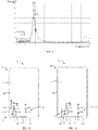


Classifications
-
- H—ELECTRICITY
- H01—ELECTRIC ELEMENTS
- H01Q—ANTENNAS, i.e. RADIO AERIALS
- H01Q9/00—Electrically-short antennas having dimensions not more than twice the operating wavelength and consisting of conductive active radiating elements
- H01Q9/04—Resonant antennas
- H01Q9/30—Resonant antennas with feed to end of elongated active element, e.g. unipole
- H01Q9/42—Resonant antennas with feed to end of elongated active element, e.g. unipole with folded element, the folded parts being spaced apart a small fraction of the operating wavelength
-
- H—ELECTRICITY
- H01—ELECTRIC ELEMENTS
- H01Q—ANTENNAS, i.e. RADIO AERIALS
- H01Q3/00—Arrangements for changing or varying the orientation or the shape of the directional pattern of the waves radiated from an antenna or antenna system
- H01Q3/24—Arrangements for changing or varying the orientation or the shape of the directional pattern of the waves radiated from an antenna or antenna system varying the orientation by switching energy from one active radiating element to another, e.g. for beam switching
-
- H—ELECTRICITY
- H01—ELECTRIC ELEMENTS
- H01Q—ANTENNAS, i.e. RADIO AERIALS
- H01Q1/00—Details of, or arrangements associated with, antennas
- H01Q1/12—Supports; Mounting means
- H01Q1/22—Supports; Mounting means by structural association with other equipment or articles
- H01Q1/24—Supports; Mounting means by structural association with other equipment or articles with receiving set
- H01Q1/241—Supports; Mounting means by structural association with other equipment or articles with receiving set used in mobile communications, e.g. GSM
-
- H—ELECTRICITY
- H01—ELECTRIC ELEMENTS
- H01Q—ANTENNAS, i.e. RADIO AERIALS
- H01Q1/00—Details of, or arrangements associated with, antennas
- H01Q1/12—Supports; Mounting means
- H01Q1/22—Supports; Mounting means by structural association with other equipment or articles
- H01Q1/24—Supports; Mounting means by structural association with other equipment or articles with receiving set
- H01Q1/241—Supports; Mounting means by structural association with other equipment or articles with receiving set used in mobile communications, e.g. GSM
- H01Q1/242—Supports; Mounting means by structural association with other equipment or articles with receiving set used in mobile communications, e.g. GSM specially adapted for hand-held use
- H01Q1/243—Supports; Mounting means by structural association with other equipment or articles with receiving set used in mobile communications, e.g. GSM specially adapted for hand-held use with built-in antennas
-
- H—ELECTRICITY
- H01—ELECTRIC ELEMENTS
- H01Q—ANTENNAS, i.e. RADIO AERIALS
- H01Q5/00—Arrangements for simultaneous operation of antennas on two or more different wavebands, e.g. dual-band or multi-band arrangements
- H01Q5/30—Arrangements for providing operation on different wavebands
- H01Q5/307—Individual or coupled radiating elements, each element being fed in an unspecified way
- H01Q5/314—Individual or coupled radiating elements, each element being fed in an unspecified way using frequency dependent circuits or components, e.g. trap circuits or capacitors
- H01Q5/328—Individual or coupled radiating elements, each element being fed in an unspecified way using frequency dependent circuits or components, e.g. trap circuits or capacitors between a radiating element and ground
-
- H—ELECTRICITY
- H01—ELECTRIC ELEMENTS
- H01Q—ANTENNAS, i.e. RADIO AERIALS
- H01Q5/00—Arrangements for simultaneous operation of antennas on two or more different wavebands, e.g. dual-band or multi-band arrangements
- H01Q5/30—Arrangements for providing operation on different wavebands
- H01Q5/307—Individual or coupled radiating elements, each element being fed in an unspecified way
- H01Q5/314—Individual or coupled radiating elements, each element being fed in an unspecified way using frequency dependent circuits or components, e.g. trap circuits or capacitors
- H01Q5/335—Individual or coupled radiating elements, each element being fed in an unspecified way using frequency dependent circuits or components, e.g. trap circuits or capacitors at the feed, e.g. for impedance matching
-
- H—ELECTRICITY
- H01—ELECTRIC ELEMENTS
- H01Q—ANTENNAS, i.e. RADIO AERIALS
- H01Q5/00—Arrangements for simultaneous operation of antennas on two or more different wavebands, e.g. dual-band or multi-band arrangements
- H01Q5/30—Arrangements for providing operation on different wavebands
- H01Q5/307—Individual or coupled radiating elements, each element being fed in an unspecified way
- H01Q5/342—Individual or coupled radiating elements, each element being fed in an unspecified way for different propagation modes
- H01Q5/35—Individual or coupled radiating elements, each element being fed in an unspecified way for different propagation modes using two or more simultaneously fed points
Definitions
- This disclosure relates to the technical field of communications, and in particular to an electronic device.
- the electronic device includes a middle frame, a first excitation source, a second excitation source, a first filtering circuit, and a second filtering circuit.
- the middle frame includes a middle-frame body and an edge frame connected with the middle-frame body at a periphery of the middle-frame body, the middle-frame body defines a first gap penetrating through two opposite surfaces of the middle-frame body, the edge frame which is adjacent to the first gap further defines a second gap, the second gap communicates with the first gap, and the first gap and the second gap are configured to divide the edge frame to form a first branch.
- the first excitation source is electrically coupled with one end of the first branch and configured to feed a first excitation signal to the first branch, to excite the first branch to resonate in a first frequency band as a first antenna of a radiator.
- the second excitation source is electrically coupled with another end of the first branch and configured to feed a second excitation signal to the first branch, to excite the first branch to resonate in a second frequency band as a second antenna of the radiator.
- a first filtering circuit is electrically coupled between the first excitation source and the first branch, and configured to filter an interference of an electromagnetic wave signal of the second frequency band to the first antenna.
- a second filtering circuit is electrically coupled between the second excitation source and the first branch, and configured to filter an interference of an electromagnetic wave signal of the first frequency band to the second antenna.
- the electronic device includes a housing and a circuit board.
- the housing includes a body and an edge frame connected with a periphery of the body, the body includes a first surface and a second surface opposite to the first surface, the body defines a first gap at the periphery of the body and the first gap penetrates through the first surface and the second surface, the first gap is configured to separate at least a part of the edge frame from the body, the edge frame defines a second gap communicating with the first gap, the first gap and the second gap are configured to divide the edge frame to form a first branch, and the first branch has a first feeding point and a second feeding point spaced apart from the first feeding point.
- the circuit board includes a first excitation source, a second excitation source, a first filtering circuit, and a second filtering circuit, the first excitation source is electrically coupled with the first feeding point, the second excitation source is electrically coupled with the second feeding point, the first filtering circuit is configured to filter an interference of a second antenna where the second excitation source is located to a first antenna where the first excitation source is located, and the second filtering circuit is configured to filter an interference of the first antenna where the first excitation source is located to the second antenna where the second excitation source is located.
- the electronic device includes a middle frame, a first excitation source, a second excitation source, a first filtering circuit, and a second filtering circuit.
- the middle frame includes a middle-frame body and an edge frame connected with the middle-frame body at a periphery of the middle-frame body, the middle-frame body defines a first gap penetrating through two opposite surfaces of the middle-frame body, the edge frame which is adjacent to the first gap further defines a second gap, the second gap communicates with the first gap, and the first gap and the second gap are configured to divide the edge frame to form a first branch.
- the first excitation source is electrically coupled with one end of the first branch and configured to feed a first excitation signal to the first branch, to excite the first branch to resonate in a first frequency band as a first antenna of a radiator.
- the second excitation source is electrically coupled with another end of the first branch and configured to feed a second excitation signal to the first branch, to excite the first branch to resonate in a second frequency band as a second antenna of the radiator.
- the first filtering circuit is electrically coupled between the first excitation source and the first branch, and configured to filter an interference of an electromagnetic wave signal of the second frequency band to the first antenna.
- the second filtering circuit is electrically coupled between the second excitation source and the first branch, and configured to filter an interference of an electromagnetic wave signal of the first frequency band to the second antenna.
- the electronic device further includes a switching circuit.
- the switching circuit is coupled in parallel with the second filtering circuit and configured to adjust a frequency-band range of the second antenna.
- a length dimension of the first branch between a feeding point of the first branch electrically coupled with the second excitation source and an end of the first branch adjacent to the second gap is: ( ⁇ 20 /4) ⁇ 5 mm, ⁇ 20 being a wavelength corresponding to a center frequency of the electromagnetic wave signal of the second frequency band.
- the second antenna further includes a voltage divider circuit, the voltage divider circuit has one end electrically coupled with the second excitation source and another end electrically coupled with one of two coupling points not coupled with a second branch, the two coupling points are formed by parallel coupling of the second filtering circuit and the switching circuit, and the voltage divider circuit coordinates with the second filtering circuit to make a voltage applied to two ends of the switching circuit less than a preset voltage.
- the switching circuit includes a switch and multiple adjusting sub-circuits, and when at least one or all of the multiple adjusting sub-circuits is electrically coupled with the first branch through the switch, the multiple adjusting sub-circuits are configured to adjust the frequency-band range of the second antenna.
- the second gap is defined corresponding to a non-end portion of the first gap, the first gap and the second gap are further configured to divide the edge frame to form a second branch, the second antenna further includes a first adjusting circuit, the first adjusting circuit has one end electrically coupled with the second branch and another end grounded, a frequency band of an electromagnetic wave signal received and transmitted by the second antenna through the second branch is different from a frequency band of an electromagnetic wave signal received and transmitted by the second antenna through the first branch, and the first adjusting circuit is configured to adjust the frequency band of the electromagnetic wave signal received and transmitted by the second antenna through the second branch.
- the edge frame includes a first edge frame and a second edge frame which are connected in a bent manner, the first gap is corresponding to the first edge frame and the second edge frame, the second gap is defined at the second edge frame, and the second branch includes a part of the second edge frame corresponding to the first gap and the second gap.
- the edge frame is implemented as at least one edge frame, the first gap is defined corresponding to one of the at least one edge frame, and the second gap is defined at the edge frame corresponding to the first gap.
- the first antenna further includes a second adjusting circuit, the second adjusting circuit has one end electrically coupled with the first branch and another end grounded, and the second adjusting circuit is configured to adjust a frequency-band range of the first antenna.
- the first antenna further includes an impedance matching circuit, the impedance matching circuit has one end electrically coupled with the first excitation source and another end electrically coupled with the first filtering circuit, and the impedance matching circuit is configured to match an output impedance of the first excitation source and an input impedance of the first branch.
- the second gap is defined corresponding to an end portion of the first gap.
- the electronic device includes a housing and a circuit board.
- the housing includes a body and an edge frame connected with a periphery of the body, the body defines a first gap at the periphery of the body and the first gap penetrates through two opposite surfaces of the body, the first gap is configured to separate at least a part of the edge frame from the body, the edge frame defines a second gap communicating with the first gap, the first gap and the second gap are configured to divide the edge frame to form a first branch, and the first branch has a first feeding point and a second feeding point spaced apart from the first feeding point.
- the circuit board includes a first excitation source, a second excitation source, a first filtering circuit, and a second filtering circuit, the first excitation source is electrically coupled with the first feeding point, the second excitation source is electrically coupled with the second feeding point, the first filtering circuit is configured to filter an interference of a second antenna where the second excitation source is located to a first antenna where the first excitation source is located, and the second filtering circuit is configured to filter an interference of the first antenna where the first excitation source is located to the second antenna where the second excitation source is located.
- the first antenna is configured to resonate in a first frequency band
- the second antenna is configured to resonate in a second frequency band
- a frequency of the first frequency band is less than a frequency of the second frequency band
- the second feeding point is more adjacent to the second gap than the first feeding point
- the first filtering circuit is a low-pass filtering circuit
- the second filtering circuit is a band-stop filtering circuit.
- the circuit board is further provided with a switching circuit, the switching circuit is coupled in parallel with the second filtering circuit, and the switching circuit is configured to adjust a frequency-band range of the second antenna.
- a length dimension between the second feeding point and an end of the first branch adjacent to the second gap is: ( ⁇ 20 /4) ⁇ 5 mm, ⁇ 20 being a wavelength corresponding to a center frequency of an electromagnetic wave signal of the second frequency band.
- the circuit board is further provided with a voltage divider circuit, the voltage divider circuit has one end electrically coupled with the second excitation source and another end electrically coupled with the second filtering circuit, and the voltage divider circuit coordinates with the second filtering circuit to make a voltage applied to two ends of the switching circuit less than a preset voltage.
- the voltage divider circuit and the second filtering circuit each include an inductor.
- a frequency of a first frequency band is less than a frequency of a second frequency band
- the first branch has a length of ( ⁇ 10 /4) ⁇ 5 mm, ⁇ 10 being a wavelength corresponding to a center frequency of an electromagnetic wave signal of the first frequency band
- the first excitation source is configured to excite the first branch to resonate in the first frequency band as the first antenna of a radiator
- the second excitation source is configured to excite the first branch to resonate in the second frequency band as the second antenna of the radiator.
- the edge frame includes a first edge frame and a second edge frame which are connected in a bent manner, the first gap is corresponding to a part of the first edge frame and a part of the second edge frame, the second gap is defined at the second edge frame, the second gap is configured to divide the part of the second edge frame corresponding to the first gap into a first part and a second part, the first part is connected with the first edge frame, the first branch includes the first part and the part of the first edge frame corresponding to the first gap, the second part constitutes the second branch, the circuit board is further provided with a first adjusting circuit, the first adjusting circuit is electrically coupled with the second branch, the first adjusting circuit is configured to adjust a frequency band of an electromagnetic wave signal received and transmitted by the second excitation source through the second branch, and a frequency band of an electromagnetic wave signal received and transmitted by the second excitation source through the first branch is different from the frequency band of the electromagnetic wave signal received and transmitted by the second excitation source through the second branch.
- the first edge frame has a length smaller than the second edge frame, and the second gap is defined at an end of the second edge frame adjacent to the first edge frame.
- An electronic device 1 is provided in the present disclosure.
- the electronic device 1 may be, but is not limited to, any device having a communication function.
- a tablet computer a mobile phone, an e-reader, a remote control, a personal computer (PC), a notebook computer, an in-vehicle equipment, an Internet protocol television (IPTV), a wearable device, and other intelligent devices with the communication function.
- the electronic device 1 is a mobile phone.
- FIG. 1 to FIG. 5 together where FIG. 1 is a three-dimensional schematic diagram of an electronic device provided in an implementation of the present disclosure, FIG. 2 is a three-dimensional schematic diagram of an electronic device from one angle provided in an implementation of the present disclosure, FIG.
- FIG. 3 is a three-dimensional schematic diagram of the middle frame illustrated in FIG. 2 from another angle
- FIG. 4 is a top diagram of a middle frame of an electronic device provided in an implementation of the present disclosure
- FIG. 5 is a schematic diagram of a first antenna and a second antenna of an electronic device provided in an implementation of the present disclosure.
- the electronic device 1 includes a middle frame 10, a first excitation source 210, a first filtering circuit 220, a second excitation source 310, and a second filtering circuit 320.
- the middle frame 10 includes a middle-frame body 110 and an edge frame 120 connected with a periphery of the middle-frame body 110.
- the middle-frame body 110 defines a first gap 113 penetrating through two opposite surfaces of the middle-frame body 110 along an edge of the middle-frame body 110, the edge frame 120 which is adjacent to the first gap 113 further defines a second gap 1221, and the second gap 1221 communicates with the first gap 113.
- the first gap 113 and the second gap 1221 are configured to divide the edge frame to form a first branch 12a.
- the first excitation source 210 is electrically coupled with one end of the first branch 12a and configured to feed a first excitation signal to the first branch 12a, to excite the first branch 12a to resonate in a first frequency band as a first antenna 20 of a radiator.
- the second excitation source 310 is electrically coupled with another end of the first branch 12a and configured to feed a second excitation signal to the first branch, to excite the first branch 12a to resonate in a second frequency band as a second antenna 30 of the radiator.
- the first filtering circuit 220 is electrically coupled between the first excitation source 210 and the first branch 12a, and configured to filter an interference of an electromagnetic wave signal of the second frequency band to the first antenna 20.
- the second filtering circuit 320 is electrically coupled between the second excitation source 310 and the first branch 12a, and configured to filter an interference of an electromagnetic wave signal of the first frequency band to the second antenna 30.
- first”, “second”, etc. in the terms “first gap 113" and “second gap 1221”, etc., in the specification, the claims, and the above accompany drawings of the present disclosure are used to distinguish different objects, rather than describe a particular order.
- the terms “include”, “comprise”, and “have” as well as variations thereof are intended to cover a non-exclusive inclusion.
- the edge frame 120 includes a first edge frame 121 and a second edge frame 122 which are connected in a bent manner.
- the first gap 113 corresponds to a part of the first edge frame 121 and a part of the second edge frame 122.
- the second gap 1221 is configured to divide the second edge frame 122 into two parts, where a part of the second frame 122 is which are connected with the first edge frame 121 in a bent manner.
- the part of the second frame which is connected with the first edge frame 121 in a bent manner and the part of the first edge frame 121 corresponding to the first gap 113 constitute the first branch 12a.
- the first edge frame 121 is a short edge frame of the electronic device 1
- the second edge frame 122 is a long edge frame of the electronic device 1. It can be understood that in other implementations, the first edge frame 121 may also have the same length as the second edge frame 122, or have a length smaller than the second edge frame 122.
- the middle frame 10 is made of a conductive material.
- the middle frame 10 may be, but is not limited to, made of magnesium aluminum alloy.
- the middle frame 10 is substantially rectangular.
- the middle frame 10 includes the first edge frame 121 and the second edge frame 122 connected with the first edge frame 121, but it can be understood that the middle frame 10 can further include other edge frames 120.
- the middle frame 10 may include other edge frames 120 in addition to the first frame 121 and the second frame 122, and all edge frames 120 in the middle frame 10 may be sequentially connected end to end and be connected with the periphery of the middle-frame body 10.
- the middle frame 10 may also be injected with an insulating material, and the insulating material may be, but is not limited to, plastic.
- a specific structure of the middle frame 10 is not limited by the present disclosure, as long as the middle frame 10 includes the middle-frame body 110 and the edge frame 120 disposed at the periphery of the middle-frame body 110.
- the first gap 113 and the second gap 1221 are filled with non-electromagnetic shielding materials.
- the first gap 113 and the second gap 1221 may also be not filled with the non-electromagnetic shielding materials.
- the non-electromagnetic shielding materials may be, but is not limited to, plastic, etc.
- FIG. 6 is a top diagram of a middle frame of an electronic device provided in another implementation of the present disclosure.
- the middle frame 10 includes the middle-frame body 10 and at least one edge frame 120 which are connected in a bent manner and the at least one edge frame 120 is connected with a periphery the middle-frame body 110.
- the first gap 113 is defined corresponding to one of the at least one edge frame 120
- the second gap 1221 is defined at the edge frame 120 corresponding to the first gap 113.
- an edge frame 120 includes the first edge frame 121 and the second edge frame 122 which are connected in a bent manner.
- the first gap 113 is only defined corresponding to the first edge frame 121
- the second gap 1221 is also defined corresponding to the first edge frame 121
- the second gap 1221 communicates with the first gap 113.
- the second gap 1221 is configured to divide the first edge frame 121 into two parts, and the second gap 1221 communicates with the first gap 113.
- the first gap 113 is corresponding to the first edge frame 121 and the second edge frame 122 which are connected in a bent manner, and the second gap 1221 is defined at the second edge frame 122.
- the first excitation source 210 is electrically coupled with an end of the first branch 12a away from the second gap 1221 to form the first antenna 20.
- the first antenna 20 is configured to receive and transmit the electromagnetic wave signal of the first frequency band through the first branch 12a.
- the first excitation source 210 is configured to generate the first excitation signal
- the first excitation signal is applied to the first branch 12a through the first filtering circuit 220
- the first branch 12a is configured to convert the first excitation signal into the electromagnetic wave signal of the first frequency band and radiate it out.
- the first filtering circuit 220 is configured to filter the interference of the electromagnetic wave signal of the second frequency band of the second antenna 30 to the first antenna 20.
- the second excitation source is electrically coupled with the second filtering circuit 320 and the second filtering circuit 320 is electrically coupled with an end of the first branch 12a adjacent to the second gap 1221, to form the second antenna 30.
- the second antenna 30 is configured to receive and transmit the electromagnetic wave signal of the second frequency band through the first branch 12a.
- the second excitation source 310 is configured to generate the second excitation signal
- the second excitation signal is applied to the first branch 12a through the second filtering circuit 320
- the first branch 12a is configured to convert the second excitation signal into the electromagnetic wave signal of the second frequency band and radiate it out.
- the second filtering circuit 320 is configured to filter the interference of the electromagnetic wave signal of the first frequency band of the first antenna 20 to the second antenna 30.
- the first filtering circuit 220 includes a capacitor and an inductor
- the second filtering circuit 320 includes an inductor
- the first frequency band is a low frequency band of a current communication frequency band, and the first frequency band is: 0.7 GHz ⁇ f1 ⁇ 0.96 GHz.
- the second frequency band is a medium and high frequency band of the current communication frequency band, and the second frequency band f2 is: 1.45 GHz ⁇ f2 ⁇ 2.69 GHz.
- the first filtering circuit 220 is a low-pass filtering circuit
- the second filtering circuit 320 is a band-stop filtering circuit.
- a frequency-band range covered by the first frequency band includes B5 frequency band, B8 frequency band, B20 frequency band, and B28 frequency band.
- the first frequency band f1 When the first frequency band is B5 frequency band, the first frequency band f1 satisfies: 824 MHz ⁇ f1 ⁇ 894 MHz; when the first frequency band is B8 frequency band, the first frequency band f1 satisfies: 880 MHz ⁇ f1 ⁇ 960 MHz; when the first frequency band is B20 frequency band, the first frequency band f1 satisfies: 791 GHz ⁇ f1 ⁇ 862 MHZ; and when the first frequency band is B28 frequency band, the first frequency band f1 satisfies: 704 MHz ⁇ f1 ⁇ 803 MHz.
- a range covered by the second frequency band includes B1 frequency band, B3 frequency band, B32 frequency band, B40 frequency band, and B41 frequency band.
- the second frequency band f2 When the second frequency band is B1 frequency band, the second frequency band f2 satisfies: 1.92 GHz ⁇ f2 ⁇ 2.17 GHz; when the second frequency band is B3 frequency band, the second frequency band f2 satisfies: 1.71 GHz ⁇ f2 ⁇ 1.88 GHz; when the second frequency band is B32 frequency band, the second frequency band f2 satisfies: 1.45 GHz ⁇ f2 ⁇ 1.5 GHz; when the second frequency band is B40 frequency band, the second frequency band f2 satisfies: 2.3 GHz ⁇ f2 ⁇ 2.4 GHz; when the second frequency band is B41 frequency band, the second frequency band f2 satisfies: 2.5 GHz ⁇ f2 ⁇ 2.69 GHz.
- the edge frame 120 of the middle frame 10 is used as the first branch 12a, and the same first branch 12a is used to form the first antenna 20 and the second antenna 30, and an interference between the first antenna 20 and the second antenna 30 is avoided by the first filtering circuit 220 and the second filtering circuit 320, thus realizing isolation between the first antenna 20 and the second antenna 30. Therefore, the electronic device 1 of the present disclosure can realize relatively large frequency-band coverage in a limited space, realize a relatively large bandwidth, and have a relatively high communication performance.
- FIG. 7 is a schematic diagram of a first antenna and a second antenna of an electronic device provided in another implementation of the present disclosure.
- the electronic device 1 further includes a switching circuit 330, the switching circuit 330 is coupled in parallel with the second filtering circuit 320, and the switching circuit 330 is configured to adjust a frequency-band range of the second antenna 30.
- the electronic device 1 includes the electronic device 1 illustrated in FIG. 5 in combination with the switching circuit.
- FIG. 8 is a schematic diagram of a switching circuit in FIG. 7 provided in an implementation.
- the switching circuit 330 includes a switch 331 and multiple adjusting sub-circuits 332, and when at least one or all of the multiple adjusting sub-circuits 332 is electrically coupled with the first branch 12a through the switch, the multiple adjusting sub-circuits 332 are configured to adjust the frequency-band range of the second antenna 30.
- Each adjusting circuit includes at least one capacitor.
- the switch 331 is a 1 of 4 selector switch, and the switching circuit 30 includes four adjusting sub-circuits 320 which are coupled in parallel.
- the first excitation signal generated by the first excitation source 210 is transmitted to the first branch 12a through the low-pass filtering circuit.
- the switch 331 of the second antenna 30 is in an off state.
- the first filtering circuit 220 is configured to filter the interference of an electromagnetic wave of the second frequency band to the first antenna 20.
- the first filtering circuit 220 is configured to filter an electromagnetic energy with frequency band f of 1.45 GHz ⁇ f ⁇ 2.69 GHz, so as to avoid an influence of the electromagnetic energy of 1.45 GHz ⁇ f ⁇ 2.69 on the first excitation source 210.
- a length dimension of the first branch 12a between a feeding point of the first branch 12a electrically coupled with the second excitation source 310 and an end of the first branch 12a adjacent to the second gap 1221 is: ( ⁇ 20 /4) ⁇ 5 mm, ⁇ 20 being a wavelength corresponding to a center frequency of the electromagnetic wave signal of the second frequency band.
- An electrical coupling point where the switching circuit 330 is electrically coupled with the first branch 12a is the feeding point of the first branch 12a electrically coupled with the second excitation source 310.
- a coupling point where the first branch 12a is electrically coupled with the first excitation source 210 is named as a first feeding point A (as illustrated in FIG. 5 to FIG. 7 )
- a coupling point where the first branch 12a electrically is coupled with the second excitation source 310 is named as a second feeding point B (as illustrated in FIG. 5 to FIG. 7 ).
- a length dimension L of the first branch 12a between a coupling point where the first branch 12a is electrically coupled with the switching circuit 330 and the end of the first branch 12a adjacent to the gap is equal to L1+L2, where L1 is equal to a length from the second feeding point B to a connection position of the first edge frame 121 and the second edge frame 122 in the first branch 12a, and L2 is equal to a length of the second edge frame 122 in the first branch 12a.
- a length of the first branch 12a between the coupling point where the first branch 12a is electrically coupled with the switching circuit 330 and the end of the first branch 12a adjacent to the second gap 1221 is equal to a length from the second feeding point B to the end of the first branch 12a adjacent to the second gap 1221.
- the length dimension L of the first branch 12a between the coupling point where the first branch 12a is electrically coupled with the switching circuit 330 and the end of the first branch 12a adjacent to the second gap 1221 is: ( ⁇ 20 /4) ⁇ 5 mm, ⁇ 20 being the wavelength corresponding to the center frequency of the electromagnetic wave signal of the second frequency band, in this case, an electrical length of the first branch 12a for receiving and transmitting the electromagnetic wave signal of the second frequency band just matches a center frequency of the radiated electromagnetic wave signal of the second frequency band, such that the first branch 12a has a relatively great reception and transmission effect when receiving and transmitting the electromagnetic wave signal of the second frequency band.
- the second frequency band f2 is 1.45 ⁇ f2 ⁇ 2.69 GHz
- the switching circuit 330 is coupled in parallel with the second filtering circuit 320 to form two coupling points, one coupling point is electrically coupled with a second branch 12b, another coupling point is not coupled with the second branch 12b.
- the second antenna 30 further includes a voltage divider circuit 340.
- the voltage divider circuit 340 has one end electrically coupled with the second excitation source 310 and another end electrically coupled with one of two coupling points not coupled with the second branch 12b, the two coupling points are formed by parallel coupling of the switching circuit 330 and the second filtering circuit 320, and the voltage divider circuit 340 coordinates with the second filtering circuit 320 to make a voltage applied to two ends of the switching circuit 330 less than a preset voltage.
- the second antenna 30 includes both the switching circuit 330 and the voltage divider circuit 340. It can be understood that, the second antenna 30 may only include the switching circuit 330 or the voltage divider circuit 340.
- the voltage divider circuit 340 includes at least one inductor.
- the multiple inductors can be coupled in series or in parallel, or partially in series and partially in parallel.
- the second filtering circuit 320 includes an inductor.
- the voltage divider circuit 340 includes an inductor, and the second filtering circuit 320 also includes an inductor, therefore, a voltage caused by the second excitation signal will not be fully applied to the switching circuit 330, and the voltage caused by the second excitation signal will be shared by the voltage divider circuit 340, thereby reducing the voltage across the switching circuit 330, which helps to improve stability of the switching circuit 330.
- FIG. 9 is a schematic simulation diagram of a voltage across a switching circuit when a second antenna includes a voltage divider circuit and a voltage across the switching circuit when the second antenna does not include the voltage divider circuit.
- a horizontal axis represents a frequency in units of GHz
- a vertical axis represents a voltage in units of V.
- curve 1 represents a schematic simulation diagram of a voltage across the switching circuit 330 when the voltage divider circuit 340 is not included.
- Curve 2 is a schematic simulation diagram of the voltage across the switching circuit 330 when the voltage divider circuit 340 is included.
- a voltage value of curve 1 is basically greater than a voltage value of curve 2.
- the voltage value at the vertex of curve 1 is 73.6 V
- the voltage value at the vertex of curve 2 is 57.5 V. It can be seen that after the voltage divider circuit 340 is added, the voltage across the switching circuit 330 decreases by a relatively great amount of 21.9%.
- FIG. 10 is a schematic diagram of a first antenna and a second antenna of an electronic device provided in another implementation of the present disclosure.
- the second gap 1221 is defined corresponding to a non-end portion of the first gap 113, and the first gap 113 and the second gap 1221 are further configured to divide the edge frame 120 to form the second branch 12b.
- the second antenna 30 further includes a first adjusting circuit 350, and the first adjusting circuit 350 has one end electrically coupled with the second branch 12b and another end grounded.
- a frequency band of an electromagnetic wave signal received and transmitted by the second antenna 30 through the second branch 12b is different from a frequency band of an electromagnetic wave signal received and transmitted by the second antenna 30 through the first branch 12a.
- the first adjusting circuit 350 is configured to adjust the frequency band of the electromagnetic wave signal received and transmitted by the second antenna 30 through the second branch 12b.
- the second branch 12b is also referred to as a parasitic branch, and the first adjusting circuit 350 includes an adjusting capacitor.
- the frequency band of the electromagnetic wave signal received and transmitted by the second antenna 30 through the second branch 12b is different from the frequency band of the electromagnetic wave signal received and transmitted by the second antenna 30 through the first branch 12a, such that the second antenna 30 can meet requirements of a carrier aggregation (CA) technology.
- CA carrier aggregation
- the CA technology requires that the electronic device 1 has a relatively large bandwidth.
- the CA technology requires that the electronic device 1 can support B1 frequency band and B41 frequency band, the second antenna 30 can realize communication of B1 frequency band through the first branch 12a, and the second antenna 30 can realize communication of B41 frequency band through the second branch 12b and the first adjusting circuit 350.
- the electronic device 1 divides the edge frame 120 to form the second branch 12b, which makes full use of the edge frame 120 of the electronic device 1, and meets a demand for a relatively large bandwidth in a limited space of the electronic device 1 with cooperation of the first adjusting circuit 350, thereby meeting the requirements of the CA technology.
- the edge frame 120 includes the first edge frame 121 and the second edge frame 122 which are connected in a bent manner, and the first gap 113 is corresponding to the first edge frame 121 and the second edge frame 122.
- the second gap 1221 is defined at the second edge frame 122, and the second branch 12b includes a part of the second edge frame 122 corresponding to the first gap 113 and the second gap 1221.
- the second branch 12b includes a part of the second edge frame 122 located above the second gap 1221.
- FIG. 11 is a schematic diagram of a first antenna and a second antenna of an electronic device provided in yet another implementation of the present disclosure.
- a structure of the electronic device 1 provided in the implementation is basically identical to a structure of the electronic device 1 provided in FIG. 10 and related descriptions, except that the first gap 113 is defined corresponding to one of edge frames 120 and the second gap 1221 is defined on the edge frame 120 corresponding to the first gap 113.
- the first gap 113 and the second gap 1221 are corresponding to a short edge frame 120 of the electronic device 1. It can be understood that in other implementations, the first gap 113 and the second gap 1221 may also be defined corresponding to a long edge frame 120 of the electronic device 1.
- the first branch 12a includes a part of the first frame 121 located at the right side of the second gap 1221 and below the first gap 113.
- the second branch 12b includes a part of the first frame 121 located at the left side of the second gap 1221 and below the first gap 113.
- FIG. 12 is a schematic diagram of a first antenna and a second antenna of an electronic device provided in yet another implementation of the present disclosure.
- the first antenna 20 further includes a second adjusting circuit 230.
- the first antenna 20 including the second adjusting circuit 230 can be combined into the electronic device 1 provided in any of the above implementations.
- the first antenna 20 including the second adjusting circuit 230 can be combined into the electronic device 1 in FIG. 10 .
- the second adjusting circuit 230 has one end electrically coupled with the first branch 12a and another end grounded, and the second adjusting circuit 230 is configured to adjust a frequency-band range of the first antenna 20.
- a coupling point where the second adjusting circuit 230 is electrically coupled with the first branch 12a is located between the first feeding point A and the second feeding point B.
- the first antenna 20 further includes an impedance matching circuit 240.
- the impedance matching circuit 240 has one end electrically coupled with the first excitation source 210 and another end electrically coupled with the first filtering circuit 220, and the impedance matching circuit 240 is configured to match an output impedance of the first excitation source 210 and an input impedance of the first branch 12a.
- the impedance matching circuit 240 is configured to match the output impedance of the first excitation source 210 and the input impedance of the first branch 12a, such that the first excitation signal generated by the first excitation source 210 is transmitted to the first branch 12a with a relatively high efficiency, to be involved in radiation of the generated electromagnetic wave signal of the first frequency band.
- FIG. 13 is a schematic diagram of a first antenna and a second antenna of an electronic device provided in yet another implementation of the present disclosure.
- the second gap 1221 is defined corresponding to an end portion of the first gap 113.
- the first gap 113 is defined corresponding to the first edge frame 121 and the second edge frame 122.
- the second gap 1221 is defined at the second edge 122.
- the second antenna 30 does not include the second branch 12b.
- FIG. 14 is a schematic diagram of a first antenna and a second antenna of an electronic device provided in yet another implementation of the present disclosure.
- the first gap 113 is only defined corresponding to the first edge frame 121
- the second gap 1221 is also defined at the first edge frame 121
- the second gap 1221 is also defined corresponding to the end portion of the first gap 113.
- the second antenna 30 does not include the second branch 12b.
- FIG. 15 is a schematic cross-sectional diagram of an electronic device provided in another implementation of the present disclosure, taken along line I-I.
- the electronic device 1 includes a middle frame 10, a circuit board 60, a battery cover 40, and a screen 50.
- the middle frame 10 includes a middle-frame body 110 and an edge frame 120 connected with a periphery of the middle-frame body 110.
- the middle-frame body 110 includes a first surface 111 and a second surface 112 opposite to the first surface 111.
- the circuit board 60 and the battery cover 40 are arranged on the first surface 111 in sequence.
- the screen 50 is arranged on the second surface 112.
- the middle-frame body 110 defines a first gap 113 penetrating through the first surface 111 and the second surface 112, the first gap 113 is corresponding to at least one edge frame 120, a surface of the frame 120 away from the middle-frame body 110 constitutes a partial appearance surface of the electronic device 1, and the at least one edge frame 120 corresponding to the first gap 113 further defines a second gap 1221 penetrating through the appearance surface.
- the second gap 1221 communicates with the first gap 113 to divide the at least one edge frame 120 to form a first branch 12a.
- the first branch 12a includes a first feeding point A and a second feeding point B spaced apart from the first feeding point A.
- the circuit board 60 is electrically coupled with the first branch 12a through the first feeding point A to receive and transmit an electromagnetic wave signal of a first frequency band through the first branch 12a.
- the circuit board 60 is electrically coupled with the first branch 12a through the second feeding point B to receive and transmit an electromagnetic wave signal of a second frequency band through the first branch 12a.
- the edge frame 120 defining the second gap 1221 is sandwiched between the screen 50 and the battery cover 40.
- the surface of the edge frame 120 defining the second gap 1221 and away from the middle-frame body 110 constitutes the partial appearance surface of the electronic device 1.
- the screen 50 refers to a component of the electronic device 1 configured to display texts, images, videos, and other contents.
- the screen 50 may be a component only having a display function, or a component integrated with a display and touch function.
- the screen 50 also includes a screen body 510 and a cover plate 520 arranged at a side of the screen body 510 away from the middle-frame body 110, and the screen body 510 is configured to display texts, images, video, and other contents of the electronic device 1.
- the cover plate 520 is configured to protect the screen body 510.
- the battery cover 40 may be made of non-metallic materials such as glass, ceramics, etc.
- the battery cover 40 and the screen 50 are arranged on two opposite surfaces of the middle-frame body 110. The two surfaces are two surfaces through which the first gap 113 penetrates.
- the middle frame 10 is used as the first branch 12a, and the first branch 12a is used to form the radiator of the first antenna 20 and the second antenna 30, and an interference between the first antenna 20 and the second antenna 30 is avoided by the first filtering circuit 220 and the second filtering circuit 320, thus realizing isolation between the first antenna 20 and the second antenna 30. Therefore, the electronic device 1 of the present disclosure can realize relatively large frequency-band coverage in a limited space, realize a relatively large bandwidth, and have a relatively high communication performance.
- the first branch 12a only defines one second gap 1221 on the edge frame 120, and when the surface of the edge frame 120 defining the second gap 1221 and away from the middle-frame body 110 constitutes the partial appearance surface of the electronic device 1, the electronic device 1 has a relatively high appearance integrity.
- the frequency of the first frequency band is less than the frequency of the second frequency band
- the circuit board 60 is provided with a first excitation source 210, a first filtering circuit 220, a second excitation source 310, and a second filtering circuit 320.
- the first excitation source 210 is electrically coupled with the first filtering circuit 220
- the first filtering circuit 220 is electrically coupled with the first feed point A
- the second excitation source 310 is electrically coupled with the second filtering circuit 320
- the second filtering circuit 320 is electrically coupled with the second feed point B
- the first filtering circuit 220 is a low-pass filtering circuit
- the second filtering circuit 320 is a band-stop filtering circuit.
- the circuit board 60 is further provided with a switching circuit 330, the switching circuit 330 is coupled in parallel with the second filtering circuit 320, and the switching circuit 330 is configured to adjust a frequency-band range of the second antenna 30.
- a length dimension between the second feeding point B and an end of the first branch 12a adjacent to the second gap 1221 is: ( ⁇ 20 /4) ⁇ 5 mm, ⁇ 20 being a wavelength corresponding to a center frequency of an electromagnetic wave signal of the second frequency band.
- the circuit board 60 is further provided with a voltage divider circuit 340.
- the voltage divider circuit 340 has one end electrically coupled with the second excitation source 310 and another end electrically coupled with the second filtering circuit 320, and the voltage divider circuit 340 coordinates with the second filtering circuit 320 to make a voltage applied to two ends of the switching circuit 330 less than a preset voltage.
- the voltage divider circuit 340 and the second filtering circuit 320 each include an inductor.
- the frequency of the first frequency band is less than the frequency of the second frequency band
- the first branch 12a has a length of ( ⁇ 10 /4) ⁇ 5 mm, ⁇ 10 being a wavelength corresponding to a center frequency of an electromagnetic wave signal of the first frequency band.
- the length of the first branch 12a matches the central frequency point of the transmitted and received electromagnetic wave signal of the first frequency band, such that the first branch 12a has a relatively great reception and transmission effect when receiving and transmitting the electromagnetic wave signal of the first frequency band.
- the first antenna 20 is an inverted-F antenna (IFA) with a quarter wavelength. In this case, through an adjustment function of a second adjusting circuit, the first antenna 20 can completely cover a low frequency band of 0.7 ⁇ 0.96 GHz.
- the edge frame 120 includes a first edge frame 121 and a second edge frame 122 which are connected in a bent manner, the first gap 113 is corresponding to a part of the first edge frame 121 and a part of the second edge frame 122, the second gap 1221 is defined at the second edge frame 122, the second gap 1221 is configured to divide the part of the second edge frame 122 corresponding to the first gap 113 into a first part 12a and a second part 12b (reference can be made to FIG.7 ).
- the first part 12a is connected with the first edge frame 121, the first branch 12a includes the first part 12a and the part of the first edge frame 121 corresponding to the first gap 113, and the second part 12b constitutes the second branch 12b.
- the circuit board 60 is further provided with a first adjusting circuit 350, the first adjusting circuit 350 is electrically coupled with the second branch 12b, the first adjusting circuit 350 is configured to adjust a frequency band of an electromagnetic wave signal received and transmitted by the second excitation source 310 through the second branch 12b, and a frequency band of an electromagnetic wave signal received and transmitted by the second excitation source 310 through the first branch 12a is different from the frequency band of the electromagnetic wave signal received and transmitted by the second excitation source 310 through the second branch 12b.
- the first edge frame 121 has a length smaller than the second edge frame 122, and the second gap 1221 is defined at an end of the second edge frame 122 adjacent to the first edge frame 121.
- the second gap 1221 can be prevented from being held by the user, thereby avoiding degradation of the communication performance of the first antenna 20 and the second antenna 30 when the second gap 1221 is held.
- FIG. 16 is a schematic simulation diagram of S-parameters of a first antenna of an electronic device 1 provided in an implementation of the present disclosure.
- a horizontal axis represents a frequency in units of GHz
- a vertical axis represents S-parameter in units of decibel (dB).
- S-parameters are reflection coefficients, and for the antenna, each of S-parameters refers to a ratio of energy reflected back to total energy of an excitation signal generated by an excitation source of an antenna.
- curve 1 is a simulation curve of S-parameters of the first antenna 20 in B5 frequency band
- curve 2 is a simulation curve of S-parameters of the first antenna 20 in B8 CH1 sub-frequency band of B8 frequency band
- curve 3 a simulation curve of S-parameters of the first antenna 20 in B8 CH2 sub-frequency band of B8 frequency band
- curve 3 a simulation curve of S-parameters of the first antenna 20 in B8_CH3 sub-frequency band of B8 frequency band
- curve 4 is a simulation curve of S-parameters of the first antenna 20 in B20 frequency band
- curve 5 is a simulation curve of S-parameters of the first antenna 20 in B28 frequency band.
- reflection coefficients of the first antenna 20 in B5 frequency band are all less than -4 dB, and it can be seen that the reflection coefficients of the first antenna 20 in B5 frequency band are all relatively small. In other words, the first antenna 20 has relatively little energy reflected back in B5 frequency band and relatively more energy involved in the radiation. Therefore, the first antenna 20 has a relatively great communication effect in B5 frequency band. Similarly, the first antenna 20 also have relatively small reflection coefficients in B8 frequency band, B20 frequency band, and B28 frequency band.
- FIG. 17 is a schematic simulation diagram of system efficiencies of a first antenna of an electronic device provided in an implementation of the present disclosure.
- a system efficiency is equal to a radiation efficiency multiplied by a reflection coefficient, and higher system efficiency is better.
- a horizontal axis represents a frequency in units of GHz, and a vertical axis represents a system efficiency in units of dB;
- curve 1 is a simulation curve of the system efficiency of the first antenna 20 in B28 frequency band;
- curve 2 is a simulation curve of the system efficiency of the first antenna 20 in B20 frequency band;
- curve 3 is the simulation curve of the system efficiency curve of the first antenna 20 in B5 frequency band;
- curve 4 is a simulation curve of the first antenna 20 in B8_CH1 sub-frequency band of B8 frequency band;
- curve 5 is a simulation curve of the first antenna 20 in B8_CH2 sub-frequency band of B8 frequency band;
- curve 6 is a simulation curve of the first antenna 20 in B8_CH3 sub-frequency band of B8 frequency band.
- the system efficiency of B28 frequency band is about -4.5 dB, and it can be seen that the first antenna 20 has a relatively high system efficiency in B28 frequency band. Similarly, the first antenna 20 has relatively high system efficiencies in B20 frequency band, B5 frequency band, and B8 frequency band.
- FIG. 18 a schematic simulation diagram of isolation between a first antenna and a second antenna of an electronic device provided in an implementation of the present disclosure.
- a horizontal axis represents a frequency in units of GHz, and a vertical axis represents isolation in units of dB;
- curve 1 represents an energy transmitted from the second antenna 30 to the first antenna 20;
- curve 2 represents an energy transmitted from the first antenna 20 to the second antenna 30.
- curve 1 and curve 2 basically coincide.
- smaller vertical axis number is better, and smaller number represents higher isolation. It can be seen from point 3 in the schematic diagram, the numbers are (0.91734, -19.081). It can be seen that most of the isolation of the first antenna 20 and the second antenna 30 are less than -19 dB, that is, the first antenna 20 and the second antenna 30 have relatively great isolation.
- FIG. 19 is a schematic simulation diagram of S-parameters of a second antenna of an electronic device provided in an implementation of the present disclosure.
- the horizontal axis represents the frequency in units of GHz
- the vertical axis represents S-parameters in units of dB.
- S-parameters are reflection coefficients, and for the antenna, each of S-parameters refers to the ratio of the energy reflected to the total energy of the excitation signal generated by the excitation source of the antenna. Lower S-parameters are better, and in this case, for from the excitation signal generated by the excitation source of the antenna, relatively little energy is reflected back, and relatively more energy is involved in radiation.
- curve 1 is a simulation curve of S-parameters of the second antenna 30 in B1 frequency band
- curve 2 is a simulation curve of S-parameters of the second antenna 30 in B3 frequency band
- curve 3 a simulation curve of S-parameters of the second antenna 30 in B32 frequency band
- curve 4 is a simulation curve of S-parameters of the second antenna 30 in B40 frequency band
- curve 5 is a simulation curve of S-parameters of the second antenna 30 in B41 frequency band.
- S-parameters of the second antenna 30 in B1 frequency band are less than -4 dB. It can be seen that the reflection coefficients of the second antenna 30 in B1 frequency band are all relatively small.
- the second antenna 30 has relatively little energy reflected back in B1 frequency band and relatively more energy involved in the radiation. Therefore, the second antenna 30 has a relatively great communication effect in B1 frequency band. Similarly, the second antenna 30 also have relatively small reflection coefficients in B3 frequency band, B32 frequency band, B40 frequency band, and B41 frequency band.
- FIG. 20 is a schematic simulation diagram of system efficiencies of a second antenna of an electronic device provided in an implementation of the present disclosure.
- the system efficiency is equal to the radiation efficiency multiplied by the reflection coefficient, and higher the system efficiency is better.
- the horizontal axis represents the frequency in units of GHz, and the vertical axis represents the system efficiency in units of dB;
- curve 1 is a simulation curve of the system efficiency of the second antenna 30 in B3 frequency band;
- curve 2 is a simulation curve of the system efficiency of the second antenna 30 in B1 frequency band;
- curve 3 is the simulation curve of the system efficiency curve of the second antenna 30 in B32 frequency band;
- curve 4 is a simulation curve of the system efficiency of the second antenna 30 in B40 frequency band;
- curve 5 is a simulation curve of system efficiency of the second antenna 30 in B41 frequency band.
- the system efficiency of B3 frequency band is about -4 dB, and it can be seen that the second antenna 30 has a relatively high system efficiency in B3 frequency band. Similarly, the second antenna 30 has relatively high system efficiencies in B1 frequency band, B32 frequency band, B40 frequency band, and B41 frequency band.
- FIG. 21 is a schematic simulation diagram of S-parameters of a second antenna of an electronic device which includes a second branch provided in an implementation of the present disclosure includes a second branch.
- the horizontal axis represents the frequency in units of GHz
- the vertical axis represents S-parameters in units of dB.
- S-parameters are reflection coefficients, and for the antenna, each of S-parameters refers to the ratio of the energy reflected back to the total energy of the excitation signal generated by the excitation source of the antenna. Lower S-parameters are better, and in this case, for from the excitation signal generated by the excitation source of the antenna, relatively little energy is reflected back, and relatively more energy is involved in radiation.
- S-parameters of the second antenna 30 in a frequency band of 1.71 GHz-2.69 GHz are all less than -2 dB, that is, S-parameters of the second antenna 30 in the 1.71 GHz-2.69 GHz are relatively small. It can be seen that the second antenna 30 covers a relatively wide frequency band while taking account of S-parameters. Therefore, the electronic device 1 of the present disclosure has a relatively large bandwidth and a relatively great communication quality in the second frequency band where the second antenna 30 operates.
- FIG. 22 is a schematic simulation diagram of system efficiencies of a second antenna of an electronic device which includes a second branch provided in an implementation of the present disclosure includes a second branch.
- the horizontal axis represents the frequency in units of GHz
- the vertical axis represents the system efficiency in units of dB; and higher the system efficiency is better.
- Curve 1 is a simulation curve of the system efficiency when the second antenna 30 includes the second branch 12b.
- Point 1 corresponds to a system efficiency of the second antenna 30 at a lowest frequency point of B3 frequency band
- point 2 corresponds to a system efficiency of the second antenna 30 at a highest frequency point of B41 frequency band.
- the second antenna 30 includes the second branch 12b
- a corresponding frequency band is between point 1 and point 2
- the system efficiency is greater than or equal to -7.3 dB
- the second antenna 30 has a relatively high system efficiency.
- the electronic device 1 of the present disclosure has a relatively great communication effect.
- the electronic device 1 includes the middle frame 10, and the first antenna 20 and the second antenna 30 are formed on the middle frame 10.
- the first branch 12a and the second branch 12b of the first antenna 20 and the second antenna 30 may also be formed on other components.
- the electronic device 1 includes a conductive battery cover 40 (e.g., a metal battery cover)
- the first branch 12a and the second branch 12b of the first antenna 20 and the second antenna 30 may also be formed on the battery cover 40.
- the conductive battery cover 40 and the middle frame 10 are only specific forms of the housing of the electronic device 1.
- the housing is not limited to the conductive battery cover 40 and the middle frame 10 of the electronic device 1, as long as the first branch 12a and the second branch 12b of the first antenna 20 and of the second antenna 30 can be formed.
- FIG. 23 is a back side schematic diagram of an electronic device provided in an implementation of the present disclosure
- FIG. 24 is a schematic diagram of an inner surface of a battery cover of an electronic device of the present disclosure
- FIG. 25 is a schematic cross-section diagram, taken along line II-II in FIG. 23 .
- the housing 70 includes a body 710 and an edge frame 720 connected with a periphery of the body 710, the body 710 defines a first gap 113 at the periphery of the body 710 and the first gap 113 penetrates through two opposite surfaces of the body 710, the first gap 113 is configured to separate at least a part of the edge frame 720 from the body 710, the edge frame 720 defines a second gap 1221 communicating with the first gap 113.
- the housing 70 is used to form the first branch 12a, and the first branch 12a is used to form a radiator of the first antenna 20 and the second antenna 30, and an interference between the first antenna 20 and the second antenna 30 is avoided by the first filtering circuit 220 and the second filtering circuit 320, thus realizing isolation between the first antenna 20 and the second antenna 30. Therefore, the electronic device 1 of the present disclosure can realize relatively large frequency-band coverage in a limited space, realize a relatively large bandwidth, and have a relatively high communication performance.
- the housing 70 When the housing 70 is the conductive battery cover 40, the housing 70 defines an accommodating space, and the accommodating space is used to accommodate the middle frame 10, the circuit board 60, and the screen 50.
- the circuit board 60 is arranged at a side of the middle frame 10 facing the battery cover 40, and the screen 50 is arranged at a side of the circuit board 60 away from the middle frame 10.
- Circuits of the first antenna 20 and the second antenna 30 are all arranged on the circuit board 60.
- the first excitation source 210, the first filtering circuit 220, the second excitation source 310, and the second filtering circuit 320 are all arranged on the circuit board 60.
- the electronic device 1 when the housing 70 is the conductive battery cover 40, the electronic device 1 also includes various circuits and sub-circuits when the housing 70 is the middle frame 10. Reference of the various circuits can be made to the above descriptions, which will not be repeated herein.
- the housing 70 is the conductive battery cover 40, relationships between the first gap 113 and other components of the housing 70 and relationships between the second gap 1221 and other components of the housing 70 are identical to those of the implementations when the housing 70 is the middle frame 10, which will not be repeated herein.
- the first antenna 20 operates in the first frequency band and the first frequency band is: 0.7 GHz ⁇ f1 ⁇ 0.96 GHz
- the second antenna 30 operates in the second frequency band and the second frequency band is: 1.45 GHz ⁇ f2 ⁇ 2.69 GHz.
- the above introduction of the first antenna 20 and the second antenna 30 cannot be understood as limitations to the first antenna 20 and the second antenna 30 of the present disclosure.
- the first antenna 20 and the second antenna 30 may also be antennas supporting other frequency bands.
Landscapes
- Engineering & Computer Science (AREA)
- Computer Networks & Wireless Communication (AREA)
- Support Of Aerials (AREA)
- Transceivers (AREA)
- Details Of Aerials (AREA)
- Variable-Direction Aerials And Aerial Arrays (AREA)
Abstract
Description
- This disclosure relates to the technical field of communications, and in particular to an electronic device.
- With development of a mobile communication technology, smart phones with a communication function are more and more favored by users. With functions of a smart phone being increasingly more, more and more components are stacked in the smart phone, and less and less space is left for an antenna in the smart phone. The space of the antenna in the smart phone is relatively small, which leads to a limitation to clearance of the antenna and a bandwidth of the antenna. As can be seen that a communication performance of an antenna in a traditional smart phone needs to be improved.
- An electronic device is provided in the present disclosure. The electronic device includes a middle frame, a first excitation source, a second excitation source, a first filtering circuit, and a second filtering circuit. The middle frame includes a middle-frame body and an edge frame connected with the middle-frame body at a periphery of the middle-frame body, the middle-frame body defines a first gap penetrating through two opposite surfaces of the middle-frame body, the edge frame which is adjacent to the first gap further defines a second gap, the second gap communicates with the first gap, and the first gap and the second gap are configured to divide the edge frame to form a first branch. The first excitation source is electrically coupled with one end of the first branch and configured to feed a first excitation signal to the first branch, to excite the first branch to resonate in a first frequency band as a first antenna of a radiator. The second excitation source is electrically coupled with another end of the first branch and configured to feed a second excitation signal to the first branch, to excite the first branch to resonate in a second frequency band as a second antenna of the radiator. A first filtering circuit is electrically coupled between the first excitation source and the first branch, and configured to filter an interference of an electromagnetic wave signal of the second frequency band to the first antenna. A second filtering circuit is electrically coupled between the second excitation source and the first branch, and configured to filter an interference of an electromagnetic wave signal of the first frequency band to the second antenna.
- An electronic device is further provided in the present disclosure. The electronic device includes a housing and a circuit board. The housing includes a body and an edge frame connected with a periphery of the body, the body includes a first surface and a second surface opposite to the first surface, the body defines a first gap at the periphery of the body and the first gap penetrates through the first surface and the second surface, the first gap is configured to separate at least a part of the edge frame from the body, the edge frame defines a second gap communicating with the first gap, the first gap and the second gap are configured to divide the edge frame to form a first branch, and the first branch has a first feeding point and a second feeding point spaced apart from the first feeding point. The circuit board includes a first excitation source, a second excitation source, a first filtering circuit, and a second filtering circuit, the first excitation source is electrically coupled with the first feeding point, the second excitation source is electrically coupled with the second feeding point, the first filtering circuit is configured to filter an interference of a second antenna where the second excitation source is located to a first antenna where the first excitation source is located, and the second filtering circuit is configured to filter an interference of the first antenna where the first excitation source is located to the second antenna where the second excitation source is located.
- In order to describe technical solutions of the present disclosure more clearly, the following will give a brief introduction to the accompanying drawings used for describing the implementations. Apparently, the accompanying drawings hereinafter described are merely some implementations of the present disclosure. Based on these drawings, those of ordinary skill in the art can also obtain other drawings without creative effort.
-
FIG. 1 is a three-dimensional schematic diagram of an electronic device provided in an implementation of the present disclosure. -
FIG. 2 is a three-dimensional schematic diagram of an electronic device from one angle provided in an implementation of the present disclosure. -
FIG. 3 is a three-dimensional schematic diagram of the middle frame illustrated inFIG. 2 from another angle. -
FIG. 4 is a top diagram of a middle frame of an electronic device provided in an implementation of the present disclosure. -
FIG. 5 is a schematic diagram of a first antenna and a second antenna of an electronic device provided in an implementation of the present disclosure. -
FIG. 6 is a top diagram of a middle frame of an electronic device provided in another implementation of the present disclosure. -
FIG. 7 is a schematic diagram of a first antenna and a second antenna of an electronic device provided in another implementation of the present disclosure. -
FIG. 8 is a schematic diagram of a switching circuit inFIG. 7 provided in an implementation. -
FIG. 9 is a schematic simulation diagram of a voltage across a switching circuit when a second antenna includes a voltage divider circuit and a voltage across the switching circuit when the second antenna does not include the voltage divider circuit. -
FIG. 10 is a schematic diagram of a first antenna and a second antenna of an electronic device provided in another implementation of the present disclosure. -
FIG. 11 is a schematic diagram of a first antenna and a second antenna of an electronic device provided in yet another implementation of the present disclosure. -
FIG. 12 is a schematic diagram of a first antenna and a second antenna of an electronic device provided in yet another implementation of the present disclosure. -
FIG. 13 is a schematic diagram of a first antenna and a second antenna of an electronic device provided in yet another implementation of the present disclosure. -
FIG. 14 is a schematic diagram of a first antenna and a second antenna of an electronic device provided in yet another implementation of the present disclosure. -
FIG. 15 is a schematic cross-sectional diagram of an electronic device provided in another implementation of the present disclosure, taken along line I-I. -
FIG. 16 is a schematic simulation diagram of S-parameters of a first antenna of anelectronic device 1 provided in an implementation of the present disclosure. -
FIG. 17 is a schematic simulation diagram of system efficiencies of a first antenna of an electronic device provided in an implementation of the present disclosure. -
FIG. 18 is a schematic simulation diagram of isolation between a first antenna and a second antenna of an electronic device provided in an implementation of the present disclosure. -
FIG. 19 is a schematic simulation diagram of S-parameters of a second antenna of an electronic device provided in an implementation of the present disclosure. -
FIG. 20 is a schematic simulation diagram of system efficiencies of a second antenna of an electronic device provided in an implementation of the present disclosure. -
FIG. 21 is a schematic simulation diagram of S-parameters of a second antenna of an electronic device which includes a second branch provided in an implementation of the present disclosure. -
FIG. 22 is a schematic simulation diagram of system efficiencies of a second antenna of an electronic device which includes a second branch provided in an implementation of the present disclosure. -
FIG. 23 is a back side schematic diagram of an electronic device provided in an implementation of the present disclosure. -
FIG. 24 is a schematic diagram of an inner surface of a battery cover of an electronic device of the present disclosure. -
FIG. 25 is a schematic cross-section diagram, taken along line II-II inFIG. 23 . - An electronic device is provided in implementations of the present disclosure. The electronic device includes a middle frame, a first excitation source, a second excitation source, a first filtering circuit, and a second filtering circuit. The middle frame includes a middle-frame body and an edge frame connected with the middle-frame body at a periphery of the middle-frame body, the middle-frame body defines a first gap penetrating through two opposite surfaces of the middle-frame body, the edge frame which is adjacent to the first gap further defines a second gap, the second gap communicates with the first gap, and the first gap and the second gap are configured to divide the edge frame to form a first branch. The first excitation source is electrically coupled with one end of the first branch and configured to feed a first excitation signal to the first branch, to excite the first branch to resonate in a first frequency band as a first antenna of a radiator. The second excitation source is electrically coupled with another end of the first branch and configured to feed a second excitation signal to the first branch, to excite the first branch to resonate in a second frequency band as a second antenna of the radiator. The first filtering circuit is electrically coupled between the first excitation source and the first branch, and configured to filter an interference of an electromagnetic wave signal of the second frequency band to the first antenna. The second filtering circuit is electrically coupled between the second excitation source and the first branch, and configured to filter an interference of an electromagnetic wave signal of the first frequency band to the second antenna.
- The electronic device further includes a switching circuit. The switching circuit is coupled in parallel with the second filtering circuit and configured to adjust a frequency-band range of the second antenna.
- A length dimension of the first branch between a feeding point of the first branch electrically coupled with the second excitation source and an end of the first branch adjacent to the second gap is: (λ20/4) ± 5 mm, λ20 being a wavelength corresponding to a center frequency of the electromagnetic wave signal of the second frequency band.
- The second antenna further includes a voltage divider circuit, the voltage divider circuit has one end electrically coupled with the second excitation source and another end electrically coupled with one of two coupling points not coupled with a second branch, the two coupling points are formed by parallel coupling of the second filtering circuit and the switching circuit, and the voltage divider circuit coordinates with the second filtering circuit to make a voltage applied to two ends of the switching circuit less than a preset voltage.
- The switching circuit includes a switch and multiple adjusting sub-circuits, and when at least one or all of the multiple adjusting sub-circuits is electrically coupled with the first branch through the switch, the multiple adjusting sub-circuits are configured to adjust the frequency-band range of the second antenna.
- The second gap is defined corresponding to a non-end portion of the first gap, the first gap and the second gap are further configured to divide the edge frame to form a second branch, the second antenna further includes a first adjusting circuit, the first adjusting circuit has one end electrically coupled with the second branch and another end grounded, a frequency band of an electromagnetic wave signal received and transmitted by the second antenna through the second branch is different from a frequency band of an electromagnetic wave signal received and transmitted by the second antenna through the first branch, and the first adjusting circuit is configured to adjust the frequency band of the electromagnetic wave signal received and transmitted by the second antenna through the second branch.
- The edge frame includes a first edge frame and a second edge frame which are connected in a bent manner, the first gap is corresponding to the first edge frame and the second edge frame, the second gap is defined at the second edge frame, and the second branch includes a part of the second edge frame corresponding to the first gap and the second gap.
- The edge frame is implemented as at least one edge frame, the first gap is defined corresponding to one of the at least one edge frame, and the second gap is defined at the edge frame corresponding to the first gap.
- The first antenna further includes a second adjusting circuit, the second adjusting circuit has one end electrically coupled with the first branch and another end grounded, and the second adjusting circuit is configured to adjust a frequency-band range of the first antenna.
- The first antenna further includes an impedance matching circuit, the impedance matching circuit has one end electrically coupled with the first excitation source and another end electrically coupled with the first filtering circuit, and the impedance matching circuit is configured to match an output impedance of the first excitation source and an input impedance of the first branch.
- The second gap is defined corresponding to an end portion of the first gap.
- An electronic device is further provided in implementations of the present disclosure. The electronic device includes a housing and a circuit board. The housing includes a body and an edge frame connected with a periphery of the body, the body defines a first gap at the periphery of the body and the first gap penetrates through two opposite surfaces of the body, the first gap is configured to separate at least a part of the edge frame from the body, the edge frame defines a second gap communicating with the first gap, the first gap and the second gap are configured to divide the edge frame to form a first branch, and the first branch has a first feeding point and a second feeding point spaced apart from the first feeding point. The circuit board includes a first excitation source, a second excitation source, a first filtering circuit, and a second filtering circuit, the first excitation source is electrically coupled with the first feeding point, the second excitation source is electrically coupled with the second feeding point, the first filtering circuit is configured to filter an interference of a second antenna where the second excitation source is located to a first antenna where the first excitation source is located, and the second filtering circuit is configured to filter an interference of the first antenna where the first excitation source is located to the second antenna where the second excitation source is located.
- The first antenna is configured to resonate in a first frequency band, the second antenna is configured to resonate in a second frequency band, a frequency of the first frequency band is less than a frequency of the second frequency band, the second feeding point is more adjacent to the second gap than the first feeding point, the first filtering circuit is a low-pass filtering circuit, and the second filtering circuit is a band-stop filtering circuit.
- The circuit board is further provided with a switching circuit, the switching circuit is coupled in parallel with the second filtering circuit, and the switching circuit is configured to adjust a frequency-band range of the second antenna.
- A length dimension between the second feeding point and an end of the first branch adjacent to the second gap is: (λ20/4) ± 5 mm, λ20 being a wavelength corresponding to a center frequency of an electromagnetic wave signal of the second frequency band.
- The circuit board is further provided with a voltage divider circuit, the voltage divider circuit has one end electrically coupled with the second excitation source and another end electrically coupled with the second filtering circuit, and the voltage divider circuit coordinates with the second filtering circuit to make a voltage applied to two ends of the switching circuit less than a preset voltage.
- The voltage divider circuit and the second filtering circuit each include an inductor.
- A frequency of a first frequency band is less than a frequency of a second frequency band, the first branch has a length of (λ10/4) ± 5 mm, λ10 being a wavelength corresponding to a center frequency of an electromagnetic wave signal of the first frequency band, the first excitation source is configured to excite the first branch to resonate in the first frequency band as the first antenna of a radiator, and the second excitation source is configured to excite the first branch to resonate in the second frequency band as the second antenna of the radiator.
- The edge frame includes a first edge frame and a second edge frame which are connected in a bent manner, the first gap is corresponding to a part of the first edge frame and a part of the second edge frame, the second gap is defined at the second edge frame, the second gap is configured to divide the part of the second edge frame corresponding to the first gap into a first part and a second part, the first part is connected with the first edge frame, the first branch includes the first part and the part of the first edge frame corresponding to the first gap, the second part constitutes the second branch, the circuit board is further provided with a first adjusting circuit, the first adjusting circuit is electrically coupled with the second branch, the first adjusting circuit is configured to adjust a frequency band of an electromagnetic wave signal received and transmitted by the second excitation source through the second branch, and a frequency band of an electromagnetic wave signal received and transmitted by the second excitation source through the first branch is different from the frequency band of the electromagnetic wave signal received and transmitted by the second excitation source through the second branch.
- The first edge frame has a length smaller than the second edge frame, and the second gap is defined at an end of the second edge frame adjacent to the first edge frame.
- Technical solutions of implementations of the present disclosure will be described clearly and completely with reference to accompanying drawings in the implementations of the present disclosure below. Apparently, the implementations described herein are merely some implementations, rather than all implementations, of the present disclosure. Based on the implementations of the present disclosure, all other implementations obtained by those of ordinary skill in the art without creative effort shall fall within the protection scope of the present disclosure.
- The term "implementation" referred to herein means that a particular feature, structure, or feature described in connection with the implementation may be contained in at least one implementation of the present disclosure. The phrase appearing in various places in the specification does not necessarily refer to the same implementation, nor does it refer an independent or alternative implementation that is mutually exclusive with other implementations. It is expressly and implicitly understood by those skilled in the art that the implementations described herein may be combined with other implementations.
- An
electronic device 1 is provided in the present disclosure. Theelectronic device 1 may be, but is not limited to, any device having a communication function. For example, a tablet computer, a mobile phone, an e-reader, a remote control, a personal computer (PC), a notebook computer, an in-vehicle equipment, an Internet protocol television (IPTV), a wearable device, and other intelligent devices with the communication function. In schematic diagrams of the implementations, for example, theelectronic device 1 is a mobile phone. Reference can be made toFIG. 1 to FIG. 5 together, whereFIG. 1 is a three-dimensional schematic diagram of an electronic device provided in an implementation of the present disclosure,FIG. 2 is a three-dimensional schematic diagram of an electronic device from one angle provided in an implementation of the present disclosure,FIG. 3 is a three-dimensional schematic diagram of the middle frame illustrated inFIG. 2 from another angle,FIG. 4 is a top diagram of a middle frame of an electronic device provided in an implementation of the present disclosure, andFIG. 5 is a schematic diagram of a first antenna and a second antenna of an electronic device provided in an implementation of the present disclosure. Theelectronic device 1 includes amiddle frame 10, afirst excitation source 210, afirst filtering circuit 220, asecond excitation source 310, and asecond filtering circuit 320. Themiddle frame 10 includes a middle-frame body 110 and anedge frame 120 connected with a periphery of the middle-frame body 110. The middle-frame body 110 defines afirst gap 113 penetrating through two opposite surfaces of the middle-frame body 110 along an edge of the middle-frame body 110, theedge frame 120 which is adjacent to thefirst gap 113 further defines asecond gap 1221, and thesecond gap 1221 communicates with thefirst gap 113. Thefirst gap 113 and thesecond gap 1221 are configured to divide the edge frame to form afirst branch 12a. Thefirst excitation source 210 is electrically coupled with one end of thefirst branch 12a and configured to feed a first excitation signal to thefirst branch 12a, to excite thefirst branch 12a to resonate in a first frequency band as afirst antenna 20 of a radiator. Thesecond excitation source 310 is electrically coupled with another end of thefirst branch 12a and configured to feed a second excitation signal to the first branch, to excite thefirst branch 12a to resonate in a second frequency band as asecond antenna 30 of the radiator. Thefirst filtering circuit 220 is electrically coupled between thefirst excitation source 210 and thefirst branch 12a, and configured to filter an interference of an electromagnetic wave signal of the second frequency band to thefirst antenna 20. Thesecond filtering circuit 320 is electrically coupled between thesecond excitation source 310 and thefirst branch 12a, and configured to filter an interference of an electromagnetic wave signal of the first frequency band to thesecond antenna 30. - It should be noted that "first", "second", etc., in the terms "
first gap 113" and "second gap 1221", etc., in the specification, the claims, and the above accompany drawings of the present disclosure are used to distinguish different objects, rather than describe a particular order. In addition, the terms "include", "comprise", and "have" as well as variations thereof are intended to cover a non-exclusive inclusion. - In an implementation, the
edge frame 120 includes afirst edge frame 121 and asecond edge frame 122 which are connected in a bent manner. Thefirst gap 113 corresponds to a part of thefirst edge frame 121 and a part of thesecond edge frame 122. Thesecond gap 1221 is configured to divide thesecond edge frame 122 into two parts, where a part of thesecond frame 122 is which are connected with thefirst edge frame 121 in a bent manner. The part of the second frame which is connected with thefirst edge frame 121 in a bent manner and the part of thefirst edge frame 121 corresponding to thefirst gap 113 constitute thefirst branch 12a. - In the schematic diagrams of the implementations, for example, the
first edge frame 121 is a short edge frame of theelectronic device 1, and thesecond edge frame 122 is a long edge frame of theelectronic device 1. It can be understood that in other implementations, thefirst edge frame 121 may also have the same length as thesecond edge frame 122, or have a length smaller than thesecond edge frame 122. - The
middle frame 10 is made of a conductive material. For example, themiddle frame 10 may be, but is not limited to, made of magnesium aluminum alloy. Themiddle frame 10 is substantially rectangular. In the implementations of the present disclosure, for example, themiddle frame 10 includes thefirst edge frame 121 and thesecond edge frame 122 connected with thefirst edge frame 121, but it can be understood that themiddle frame 10 can further include other edge frames 120. In theelectronic device 1, themiddle frame 10 may include other edge frames 120 in addition to thefirst frame 121 and thesecond frame 122, and all edge frames 120 in themiddle frame 10 may be sequentially connected end to end and be connected with the periphery of the middle-frame body 10. - In an implementation, the
middle frame 10 may also be injected with an insulating material, and the insulating material may be, but is not limited to, plastic. A specific structure of themiddle frame 10 is not limited by the present disclosure, as long as themiddle frame 10 includes the middle-frame body 110 and theedge frame 120 disposed at the periphery of the middle-frame body 110. - In the implementations, for example, the
first gap 113 and thesecond gap 1221 are filled with non-electromagnetic shielding materials. In other implementations, thefirst gap 113 and thesecond gap 1221 may also be not filled with the non-electromagnetic shielding materials. The non-electromagnetic shielding materials may be, but is not limited to, plastic, etc. - It can be understood that in other implementations, reference can be made to
FIG. 6 , which is a top diagram of a middle frame of an electronic device provided in another implementation of the present disclosure. In the implementations, themiddle frame 10 includes the middle-frame body 10 and at least oneedge frame 120 which are connected in a bent manner and the at least oneedge frame 120 is connected with a periphery the middle-frame body 110. Thefirst gap 113 is defined corresponding to one of the at least oneedge frame 120, and thesecond gap 1221 is defined at theedge frame 120 corresponding to thefirst gap 113. In a schematic diagram of the implementations, anedge frame 120 includes thefirst edge frame 121 and thesecond edge frame 122 which are connected in a bent manner. Thefirst gap 113 is only defined corresponding to thefirst edge frame 121, thesecond gap 1221 is also defined corresponding to thefirst edge frame 121, and thesecond gap 1221 communicates with thefirst gap 113. In other words, thesecond gap 1221 is configured to divide thefirst edge frame 121 into two parts, and thesecond gap 1221 communicates with thefirst gap 113. - In following implementations, for example, the
first gap 113 is corresponding to thefirst edge frame 121 and thesecond edge frame 122 which are connected in a bent manner, and thesecond gap 1221 is defined at thesecond edge frame 122. - The
first excitation source 210 is electrically coupled with an end of thefirst branch 12a away from thesecond gap 1221 to form thefirst antenna 20. Thefirst antenna 20 is configured to receive and transmit the electromagnetic wave signal of the first frequency band through thefirst branch 12a. When thefirst antenna 20 is configured to transmit the electromagnetic wave signal of the first frequency band, thefirst excitation source 210 is configured to generate the first excitation signal, the first excitation signal is applied to thefirst branch 12a through thefirst filtering circuit 220, and thefirst branch 12a is configured to convert the first excitation signal into the electromagnetic wave signal of the first frequency band and radiate it out. Thefirst filtering circuit 220 is configured to filter the interference of the electromagnetic wave signal of the second frequency band of thesecond antenna 30 to thefirst antenna 20. - The second excitation source is electrically coupled with the
second filtering circuit 320 and thesecond filtering circuit 320 is electrically coupled with an end of thefirst branch 12a adjacent to thesecond gap 1221, to form thesecond antenna 30. Thesecond antenna 30 is configured to receive and transmit the electromagnetic wave signal of the second frequency band through thefirst branch 12a. When thesecond antenna 30 is configured to transmit the electromagnetic wave signal of the second frequency band, thesecond excitation source 310 is configured to generate the second excitation signal, the second excitation signal is applied to thefirst branch 12a through thesecond filtering circuit 320, and thefirst branch 12a is configured to convert the second excitation signal into the electromagnetic wave signal of the second frequency band and radiate it out. Thesecond filtering circuit 320 is configured to filter the interference of the electromagnetic wave signal of the first frequency band of thefirst antenna 20 to thesecond antenna 30. - In an implementation, the
first filtering circuit 220 includes a capacitor and an inductor, and thesecond filtering circuit 320 includes an inductor. - In an implementation, the first frequency band is a low frequency band of a current communication frequency band, and the first frequency band is: 0.7 GHz≤f1≤0.96 GHz. The second frequency band is a medium and high frequency band of the current communication frequency band, and the second frequency band f2 is: 1.45 GHz≤f2≤2.69 GHz. Accordingly, the
first filtering circuit 220 is a low-pass filtering circuit, and thesecond filtering circuit 320 is a band-stop filtering circuit. A frequency-band range covered by the first frequency band includes B5 frequency band, B8 frequency band, B20 frequency band, and B28 frequency band. When the first frequency band is B5 frequency band, the first frequency band f1 satisfies: 824 MHz≤f1≤ 894 MHz; when the first frequency band is B8 frequency band, the first frequency band f1 satisfies: 880 MHz≤f1≤960 MHz; when the first frequency band is B20 frequency band, the first frequency band f1 satisfies: 791 GHz≤f1≤862 MHZ; and when the first frequency band is B28 frequency band, the first frequency band f1 satisfies: 704 MHz≤f1≤ 803 MHz. A range covered by the second frequency band includes B1 frequency band, B3 frequency band, B32 frequency band, B40 frequency band, and B41 frequency band. When the second frequency band is B1 frequency band, the second frequency band f2 satisfies: 1.92 GHz≤f2≤2.17 GHz; when the second frequency band is B3 frequency band, the second frequency band f2 satisfies: 1.71 GHz≤f2≤1.88 GHz; when the second frequency band is B32 frequency band, the second frequency band f2 satisfies: 1.45 GHz≤f2≤1.5 GHz; when the second frequency band is B40 frequency band, the second frequency band f2 satisfies: 2.3 GHz≤f2≤2.4 GHz; when the second frequency band is B41 frequency band, the second frequency band f2 satisfies: 2.5 GHz ≤f2≤2.69 GHz. - Compared with the related art, in the
electronic device 1 of the present disclosure, theedge frame 120 of themiddle frame 10 is used as thefirst branch 12a, and the samefirst branch 12a is used to form thefirst antenna 20 and thesecond antenna 30, and an interference between thefirst antenna 20 and thesecond antenna 30 is avoided by thefirst filtering circuit 220 and thesecond filtering circuit 320, thus realizing isolation between thefirst antenna 20 and thesecond antenna 30. Therefore, theelectronic device 1 of the present disclosure can realize relatively large frequency-band coverage in a limited space, realize a relatively large bandwidth, and have a relatively high communication performance. - Reference can be made to
FIG. 7 , which is a schematic diagram of a first antenna and a second antenna of an electronic device provided in another implementation of the present disclosure. In an implementation, theelectronic device 1 further includes aswitching circuit 330, theswitching circuit 330 is coupled in parallel with thesecond filtering circuit 320, and theswitching circuit 330 is configured to adjust a frequency-band range of thesecond antenna 30. In the schematic diagram, for example, theelectronic device 1 includes theelectronic device 1 illustrated inFIG. 5 in combination with the switching circuit. - Reference can be made to
FIG. 8 , which is a schematic diagram of a switching circuit inFIG. 7 provided in an implementation. Theswitching circuit 330 includes aswitch 331 and multiple adjusting sub-circuits 332, and when at least one or all of the multiple adjusting sub-circuits 332 is electrically coupled with thefirst branch 12a through the switch, the multiple adjusting sub-circuits 332 are configured to adjust the frequency-band range of thesecond antenna 30. - The
switch 331 may be an N of M selector switch, where M>N, and both M and N are positive integers. For example, M=4, N=2, or M=4, N=1. Each adjusting circuit includes at least one capacitor. In the schematic diagram of the implementations, for example, theswitch 331 is a 1 of 4 selector switch, and the switchingcircuit 30 includes four adjustingsub-circuits 320 which are coupled in parallel. - When the
electronic device 1 includes theswitching circuit 330 and thefirst antenna 20 is operating, the first excitation signal generated by thefirst excitation source 210 is transmitted to thefirst branch 12a through the low-pass filtering circuit. In this case, theswitch 331 of thesecond antenna 30 is in an off state. Thefirst filtering circuit 220 is configured to filter the interference of an electromagnetic wave of the second frequency band to thefirst antenna 20. For example, when the first frequency band f1 is: 0.7 GHz≤f1≤0.96 GHz, and the second frequency band f2 is: 1.45 GHz≤f2≤2.69 GHz, thefirst filtering circuit 220 is configured to filter an electromagnetic energy with frequency band f of 1.45 GHz≤f≤2.69 GHz, so as to avoid an influence of the electromagnetic energy of 1.45 GHz≤f≤2.69 on thefirst excitation source 210. - In an implementation, a length dimension of the
first branch 12a between a feeding point of thefirst branch 12a electrically coupled with thesecond excitation source 310 and an end of thefirst branch 12a adjacent to thesecond gap 1221 is: (λ20/4) ± 5 mm, λ20 being a wavelength corresponding to a center frequency of the electromagnetic wave signal of the second frequency band. - An electrical coupling point where the
switching circuit 330 is electrically coupled with thefirst branch 12a is the feeding point of thefirst branch 12a electrically coupled with thesecond excitation source 310. For convenience of description, a coupling point where thefirst branch 12a is electrically coupled with thefirst excitation source 210 is named as a first feeding point A (as illustrated inFIG. 5 to FIG. 7 ), and a coupling point where thefirst branch 12a electrically is coupled with thesecond excitation source 310 is named as a second feeding point B (as illustrated inFIG. 5 to FIG. 7 ). Reference can be made toFIG. 5 again, a length dimension L of thefirst branch 12a between a coupling point where thefirst branch 12a is electrically coupled with theswitching circuit 330 and the end of thefirst branch 12a adjacent to the gap is equal to L1+L2, where L1 is equal to a length from the second feeding point B to a connection position of thefirst edge frame 121 and thesecond edge frame 122 in thefirst branch 12a, and L2 is equal to a length of thesecond edge frame 122 in thefirst branch 12a. - It can be understood that in other implementations, when the
first gap 113 is only defined corresponding to thefirst edge frame 121 and thesecond gap 1221 correspondingly penetrates through thefirst frame 121 and communicates with thefirst gap 113, a length of thefirst branch 12a between the coupling point where thefirst branch 12a is electrically coupled with theswitching circuit 330 and the end of thefirst branch 12a adjacent to thesecond gap 1221 is equal to a length from the second feeding point B to the end of thefirst branch 12a adjacent to thesecond gap 1221. - When the length dimension L of the
first branch 12a between the coupling point where thefirst branch 12a is electrically coupled with theswitching circuit 330 and the end of thefirst branch 12a adjacent to thesecond gap 1221 is: (λ20/4) ± 5 mm, λ20 being the wavelength corresponding to the center frequency of the electromagnetic wave signal of the second frequency band, in this case, an electrical length of thefirst branch 12a for receiving and transmitting the electromagnetic wave signal of the second frequency band just matches a center frequency of the radiated electromagnetic wave signal of the second frequency band, such that thefirst branch 12a has a relatively great reception and transmission effect when receiving and transmitting the electromagnetic wave signal of the second frequency band. When the second frequency band f2 is 1.45≤f2≤2.69 GHz, the center frequency of the second frequency band is f20=[(1.45+2.69)/2] GHz, where λ20=1/f20. - The
switching circuit 330 is coupled in parallel with thesecond filtering circuit 320 to form two coupling points, one coupling point is electrically coupled with asecond branch 12b, another coupling point is not coupled with thesecond branch 12b. Thesecond antenna 30 further includes avoltage divider circuit 340. Thevoltage divider circuit 340 has one end electrically coupled with thesecond excitation source 310 and another end electrically coupled with one of two coupling points not coupled with thesecond branch 12b, the two coupling points are formed by parallel coupling of theswitching circuit 330 and thesecond filtering circuit 320, and thevoltage divider circuit 340 coordinates with thesecond filtering circuit 320 to make a voltage applied to two ends of theswitching circuit 330 less than a preset voltage. In the schematic diagram of the implementations, for example, thesecond antenna 30 includes both theswitching circuit 330 and thevoltage divider circuit 340. It can be understood that, thesecond antenna 30 may only include theswitching circuit 330 or thevoltage divider circuit 340. - In an implementation, the
voltage divider circuit 340 includes at least one inductor. When thevoltage divider circuit 340 includes multiple inductors, the multiple inductors can be coupled in series or in parallel, or partially in series and partially in parallel. Thesecond filtering circuit 320 includes an inductor. Thevoltage divider circuit 340 includes an inductor, and thesecond filtering circuit 320 also includes an inductor, therefore, a voltage caused by the second excitation signal will not be fully applied to theswitching circuit 330, and the voltage caused by the second excitation signal will be shared by thevoltage divider circuit 340, thereby reducing the voltage across theswitching circuit 330, which helps to improve stability of theswitching circuit 330. - Reference can be made to
FIG. 9 , which is a schematic simulation diagram of a voltage across a switching circuit when a second antenna includes a voltage divider circuit and a voltage across the switching circuit when the second antenna does not include the voltage divider circuit. InFIG. 9 , a horizontal axis represents a frequency in units of GHz, and a vertical axis represents a voltage in units of V. In the schematic diagram,curve ① represents a schematic simulation diagram of a voltage across theswitching circuit 330 when thevoltage divider circuit 340 is not included.Curve ② is a schematic simulation diagram of the voltage across theswitching circuit 330 when thevoltage divider circuit 340 is included. In the schematic diagram, when thesecond antenna 30 operates at an identical frequency, a larger value of the horizontal axis represents a higher voltage across theswitching circuit 330. It can be seen from the schematic diagram that a voltage value ofcurve ① is basically greater than a voltage value ofcurve ②. Particularly, the voltage value at the vertex ofcurve ① is 73.6 V, and the voltage value at the vertex of curve ② (at the same frequency point as the vertex of curve ①) is 57.5 V. It can be seen that after thevoltage divider circuit 340 is added, the voltage across theswitching circuit 330 decreases by a relatively great amount of 21.9%. - Reference can be made to
FIG. 10 , which is a schematic diagram of a first antenna and a second antenna of an electronic device provided in another implementation of the present disclosure. Thesecond gap 1221 is defined corresponding to a non-end portion of thefirst gap 113, and thefirst gap 113 and thesecond gap 1221 are further configured to divide theedge frame 120 to form thesecond branch 12b. Thesecond antenna 30 further includes afirst adjusting circuit 350, and thefirst adjusting circuit 350 has one end electrically coupled with thesecond branch 12b and another end grounded. A frequency band of an electromagnetic wave signal received and transmitted by thesecond antenna 30 through thesecond branch 12b is different from a frequency band of an electromagnetic wave signal received and transmitted by thesecond antenna 30 through thefirst branch 12a. Thefirst adjusting circuit 350 is configured to adjust the frequency band of the electromagnetic wave signal received and transmitted by thesecond antenna 30 through thesecond branch 12b. - The
second branch 12b is also referred to as a parasitic branch, and thefirst adjusting circuit 350 includes an adjusting capacitor. - The frequency band of the electromagnetic wave signal received and transmitted by the
second antenna 30 through thesecond branch 12b is different from the frequency band of the electromagnetic wave signal received and transmitted by thesecond antenna 30 through thefirst branch 12a, such that thesecond antenna 30 can meet requirements of a carrier aggregation (CA) technology. The CA technology requires that theelectronic device 1 has a relatively large bandwidth. For example, the CA technology requires that theelectronic device 1 can support B1 frequency band and B41 frequency band, thesecond antenna 30 can realize communication of B1 frequency band through thefirst branch 12a, and thesecond antenna 30 can realize communication of B41 frequency band through thesecond branch 12b and thefirst adjusting circuit 350. It can be seen that theelectronic device 1 divides theedge frame 120 to form thesecond branch 12b, which makes full use of theedge frame 120 of theelectronic device 1, and meets a demand for a relatively large bandwidth in a limited space of theelectronic device 1 with cooperation of thefirst adjusting circuit 350, thereby meeting the requirements of the CA technology. - In the implementations, the
edge frame 120 includes thefirst edge frame 121 and thesecond edge frame 122 which are connected in a bent manner, and thefirst gap 113 is corresponding to thefirst edge frame 121 and thesecond edge frame 122. Thesecond gap 1221 is defined at thesecond edge frame 122, and thesecond branch 12b includes a part of thesecond edge frame 122 corresponding to thefirst gap 113 and thesecond gap 1221. - In the schematic diagram of the implementations, the
second branch 12b includes a part of thesecond edge frame 122 located above thesecond gap 1221. - Reference can be made to
FIG. 11 , which is a schematic diagram of a first antenna and a second antenna of an electronic device provided in yet another implementation of the present disclosure. A structure of theelectronic device 1 provided in the implementation is basically identical to a structure of theelectronic device 1 provided inFIG. 10 and related descriptions, except that thefirst gap 113 is defined corresponding to one of edge frames 120 and thesecond gap 1221 is defined on theedge frame 120 corresponding to thefirst gap 113. - In the schematic diagram of the implementation, for example, the
first gap 113 and thesecond gap 1221 are corresponding to ashort edge frame 120 of theelectronic device 1. It can be understood that in other implementations, thefirst gap 113 and thesecond gap 1221 may also be defined corresponding to along edge frame 120 of theelectronic device 1. In the implementation, thefirst branch 12a includes a part of thefirst frame 121 located at the right side of thesecond gap 1221 and below thefirst gap 113. Accordingly, thesecond branch 12b includes a part of thefirst frame 121 located at the left side of thesecond gap 1221 and below thefirst gap 113. - Reference can be made to
FIG. 12 , which is a schematic diagram of a first antenna and a second antenna of an electronic device provided in yet another implementation of the present disclosure. In the implementations, thefirst antenna 20 further includes asecond adjusting circuit 230. Thefirst antenna 20 including thesecond adjusting circuit 230 can be combined into theelectronic device 1 provided in any of the above implementations. In the schematic diagram of the implementations, for example, thefirst antenna 20 including thesecond adjusting circuit 230 can be combined into theelectronic device 1 inFIG. 10 . Thesecond adjusting circuit 230 has one end electrically coupled with thefirst branch 12a and another end grounded, and thesecond adjusting circuit 230 is configured to adjust a frequency-band range of thefirst antenna 20. - Specifically, a coupling point where the
second adjusting circuit 230 is electrically coupled with thefirst branch 12a is located between the first feeding point A and the second feeding point B. - In an implementation, the
first antenna 20 further includes animpedance matching circuit 240. Theimpedance matching circuit 240 has one end electrically coupled with thefirst excitation source 210 and another end electrically coupled with thefirst filtering circuit 220, and theimpedance matching circuit 240 is configured to match an output impedance of thefirst excitation source 210 and an input impedance of thefirst branch 12a. Theimpedance matching circuit 240 is configured to match the output impedance of thefirst excitation source 210 and the input impedance of thefirst branch 12a, such that the first excitation signal generated by thefirst excitation source 210 is transmitted to thefirst branch 12a with a relatively high efficiency, to be involved in radiation of the generated electromagnetic wave signal of the first frequency band. - Reference can be made to
FIG. 13 , which is a schematic diagram of a first antenna and a second antenna of an electronic device provided in yet another implementation of the present disclosure. In the schematic diagram of the implementation, thesecond gap 1221 is defined corresponding to an end portion of thefirst gap 113. Specifically, in the implementations, thefirst gap 113 is defined corresponding to thefirst edge frame 121 and thesecond edge frame 122. Thesecond gap 1221 is defined at thesecond edge 122. In this case, thesecond antenna 30 does not include thesecond branch 12b. - Reference can be made to
FIG. 14 , which is a schematic diagram of a first antenna and a second antenna of an electronic device provided in yet another implementation of the present disclosure. In the implementations, thefirst gap 113 is only defined corresponding to thefirst edge frame 121, thesecond gap 1221 is also defined at thefirst edge frame 121, and thesecond gap 1221 is also defined corresponding to the end portion of thefirst gap 113. In this case, thesecond antenna 30 does not include thesecond branch 12b. - Reference can be made to
FIG. 15 ,FIG. 1, FIG. 2 , and other related accompanying drawings together, andFIG. 15 is a schematic cross-sectional diagram of an electronic device provided in another implementation of the present disclosure, taken along line I-I. Theelectronic device 1 includes amiddle frame 10, acircuit board 60, abattery cover 40, and ascreen 50. Themiddle frame 10 includes a middle-frame body 110 and anedge frame 120 connected with a periphery of the middle-frame body 110. The middle-frame body 110 includes afirst surface 111 and asecond surface 112 opposite to thefirst surface 111. Thecircuit board 60 and thebattery cover 40 are arranged on thefirst surface 111 in sequence. Thescreen 50 is arranged on thesecond surface 112. The middle-frame body 110 defines afirst gap 113 penetrating through thefirst surface 111 and thesecond surface 112, thefirst gap 113 is corresponding to at least oneedge frame 120, a surface of theframe 120 away from the middle-frame body 110 constitutes a partial appearance surface of theelectronic device 1, and the at least oneedge frame 120 corresponding to thefirst gap 113 further defines asecond gap 1221 penetrating through the appearance surface. Thesecond gap 1221 communicates with thefirst gap 113 to divide the at least oneedge frame 120 to form afirst branch 12a. Thefirst branch 12a includes a first feeding point A and a second feeding point B spaced apart from the first feeding point A. Thecircuit board 60 is electrically coupled with thefirst branch 12a through the first feeding point A to receive and transmit an electromagnetic wave signal of a first frequency band through thefirst branch 12a. Thecircuit board 60 is electrically coupled with thefirst branch 12a through the second feeding point B to receive and transmit an electromagnetic wave signal of a second frequency band through thefirst branch 12a. - The
edge frame 120 defining thesecond gap 1221 is sandwiched between thescreen 50 and thebattery cover 40. The surface of theedge frame 120 defining thesecond gap 1221 and away from the middle-frame body 110 constitutes the partial appearance surface of theelectronic device 1. - The
screen 50 refers to a component of theelectronic device 1 configured to display texts, images, videos, and other contents. Thescreen 50 may be a component only having a display function, or a component integrated with a display and touch function. In the implementations, thescreen 50 also includes ascreen body 510 and acover plate 520 arranged at a side of thescreen body 510 away from the middle-frame body 110, and thescreen body 510 is configured to display texts, images, video, and other contents of theelectronic device 1. Thecover plate 520 is configured to protect thescreen body 510. - The
battery cover 40 may be made of non-metallic materials such as glass, ceramics, etc. Thebattery cover 40 and thescreen 50 are arranged on two opposite surfaces of the middle-frame body 110. The two surfaces are two surfaces through which thefirst gap 113 penetrates. - Compared with the related art, in the
electronic device 1 of the present disclosure, themiddle frame 10 is used as thefirst branch 12a, and thefirst branch 12a is used to form the radiator of thefirst antenna 20 and thesecond antenna 30, and an interference between thefirst antenna 20 and thesecond antenna 30 is avoided by thefirst filtering circuit 220 and thesecond filtering circuit 320, thus realizing isolation between thefirst antenna 20 and thesecond antenna 30. Therefore, theelectronic device 1 of the present disclosure can realize relatively large frequency-band coverage in a limited space, realize a relatively large bandwidth, and have a relatively high communication performance. - In addition, in the present disclosure, the
first branch 12a only defines onesecond gap 1221 on theedge frame 120, and when the surface of theedge frame 120 defining thesecond gap 1221 and away from the middle-frame body 110 constitutes the partial appearance surface of theelectronic device 1, theelectronic device 1 has a relatively high appearance integrity. - In an implementation, the frequency of the first frequency band is less than the frequency of the second frequency band, and the
circuit board 60 is provided with afirst excitation source 210, afirst filtering circuit 220, asecond excitation source 310, and asecond filtering circuit 320. Thefirst excitation source 210 is electrically coupled with thefirst filtering circuit 220, thefirst filtering circuit 220 is electrically coupled with the first feed point A, thesecond excitation source 310 is electrically coupled with thesecond filtering circuit 320, thesecond filtering circuit 320 is electrically coupled with the second feed point B, thefirst filtering circuit 220 is a low-pass filtering circuit, and thesecond filtering circuit 320 is a band-stop filtering circuit. - Reference of the
first excitation source 210, thefirst filtering circuit 220, thesecond excitation source 310, and thesecond filtering circuit 320, can be made to the above related descriptions, which will not be repeated herein. - In an implementation, the
circuit board 60 is further provided with aswitching circuit 330, theswitching circuit 330 is coupled in parallel with thesecond filtering circuit 320, and theswitching circuit 330 is configured to adjust a frequency-band range of thesecond antenna 30. - In an implementation, a length dimension between the second feeding point B and an end of the
first branch 12a adjacent to thesecond gap 1221 is: (λ20/4) ± 5 mm, λ20 being a wavelength corresponding to a center frequency of an electromagnetic wave signal of the second frequency band. - In an implementation, the
circuit board 60 is further provided with avoltage divider circuit 340. Thevoltage divider circuit 340 has one end electrically coupled with thesecond excitation source 310 and another end electrically coupled with thesecond filtering circuit 320, and thevoltage divider circuit 340 coordinates with thesecond filtering circuit 320 to make a voltage applied to two ends of theswitching circuit 330 less than a preset voltage. - In an implementation, the
voltage divider circuit 340 and thesecond filtering circuit 320 each include an inductor. - In an implementation, the frequency of the first frequency band is less than the frequency of the second frequency band, the
first branch 12a has a length of (λ10/4) ± 5 mm, λ10 being a wavelength corresponding to a center frequency of an electromagnetic wave signal of the first frequency band. - When the first branch has the length of (λ10/4) ± 5 mm, the length of the
first branch 12a matches the central frequency point of the transmitted and received electromagnetic wave signal of the first frequency band, such that thefirst branch 12a has a relatively great reception and transmission effect when receiving and transmitting the electromagnetic wave signal of the first frequency band. It can be understood that thefirst antenna 20 is an inverted-F antenna (IFA) with a quarter wavelength. In this case, through an adjustment function of a second adjusting circuit, thefirst antenna 20 can completely cover a low frequency band of 0.7~0.96 GHz. - In an implementation, the
edge frame 120 includes afirst edge frame 121 and asecond edge frame 122 which are connected in a bent manner, thefirst gap 113 is corresponding to a part of thefirst edge frame 121 and a part of thesecond edge frame 122, thesecond gap 1221 is defined at thesecond edge frame 122, thesecond gap 1221 is configured to divide the part of thesecond edge frame 122 corresponding to thefirst gap 113 into afirst part 12a and asecond part 12b (reference can be made toFIG.7 ). Thefirst part 12a is connected with thefirst edge frame 121, thefirst branch 12a includes thefirst part 12a and the part of thefirst edge frame 121 corresponding to thefirst gap 113, and thesecond part 12b constitutes thesecond branch 12b. Thecircuit board 60 is further provided with afirst adjusting circuit 350, thefirst adjusting circuit 350 is electrically coupled with thesecond branch 12b, thefirst adjusting circuit 350 is configured to adjust a frequency band of an electromagnetic wave signal received and transmitted by thesecond excitation source 310 through thesecond branch 12b, and a frequency band of an electromagnetic wave signal received and transmitted by thesecond excitation source 310 through thefirst branch 12a is different from the frequency band of the electromagnetic wave signal received and transmitted by thesecond excitation source 310 through thesecond branch 12b. - In an implementation, the
first edge frame 121 has a length smaller than thesecond edge frame 122, and thesecond gap 1221 is defined at an end of thesecond edge frame 122 adjacent to thefirst edge frame 121. - In the implementations, when a user holds the
electronic device 1 by hand, thesecond gap 1221 can be prevented from being held by the user, thereby avoiding degradation of the communication performance of thefirst antenna 20 and thesecond antenna 30 when thesecond gap 1221 is held. - In order to explain a performance of the
electronic device 1 provided in the present disclosure, various parameters of theelectronic device 1 provided in the present disclosure are simulated below. Reference can be made toFIG. 16 , which is a schematic simulation diagram of S-parameters of a first antenna of anelectronic device 1 provided in an implementation of the present disclosure. In the schematic simulation diagram, a horizontal axis represents a frequency in units of GHz, and a vertical axis represents S-parameter in units of decibel (dB). S-parameters are reflection coefficients, and for the antenna, each of S-parameters refers to a ratio of energy reflected back to total energy of an excitation signal generated by an excitation source of an antenna. Lower S-parameters are better, and in this case, for from the excitation signal generated by the excitation source of the antenna, relatively little energy is reflected back, and relatively more energy is involved in radiation. In the schematic simulation diagram,curve ① is a simulation curve of S-parameters of thefirst antenna 20 in B5 frequency band;curve ② is a simulation curve of S-parameters of thefirst antenna 20 in B8 CH1 sub-frequency band of B8 frequency band; curve ③ a simulation curve of S-parameters of thefirst antenna 20 in B8 CH2 sub-frequency band of B8 frequency band; curve ③ a simulation curve of S-parameters of thefirst antenna 20 in B8_CH3 sub-frequency band of B8 frequency band;curve ④ is a simulation curve of S-parameters of thefirst antenna 20 in B20 frequency band; andcurve ⑤ is a simulation curve of S-parameters of thefirst antenna 20 in B28 frequency band. Takingcurve ① as an example, reflection coefficients of thefirst antenna 20 in B5 frequency band are all less than -4 dB, and it can be seen that the reflection coefficients of thefirst antenna 20 in B5 frequency band are all relatively small. In other words, thefirst antenna 20 has relatively little energy reflected back in B5 frequency band and relatively more energy involved in the radiation. Therefore, thefirst antenna 20 has a relatively great communication effect in B5 frequency band. Similarly, thefirst antenna 20 also have relatively small reflection coefficients in B8 frequency band, B20 frequency band, and B28 frequency band. - Reference can be made to
FIG. 17 , which is a schematic simulation diagram of system efficiencies of a first antenna of an electronic device provided in an implementation of the present disclosure. A system efficiency is equal to a radiation efficiency multiplied by a reflection coefficient, and higher system efficiency is better. In the schematic diagram, a horizontal axis represents a frequency in units of GHz, and a vertical axis represents a system efficiency in units of dB;curve ① is a simulation curve of the system efficiency of thefirst antenna 20 in B28 frequency band;curve ② is a simulation curve of the system efficiency of thefirst antenna 20 in B20 frequency band;curve ③ is the simulation curve of the system efficiency curve of thefirst antenna 20 in B5 frequency band;curve ④ is a simulation curve of thefirst antenna 20 in B8_CH1 sub-frequency band of B8 frequency band;curve ⑤ is a simulation curve of thefirst antenna 20 in B8_CH2 sub-frequency band of B8 frequency band; andcurve ⑥ is a simulation curve of thefirst antenna 20 in B8_CH3 sub-frequency band of B8 frequency band. Takingcurve ① as an example, the system efficiency of B28 frequency band is about -4.5 dB, and it can be seen that thefirst antenna 20 has a relatively high system efficiency in B28 frequency band. Similarly, thefirst antenna 20 has relatively high system efficiencies in B20 frequency band, B5 frequency band, and B8 frequency band. - Reference can be made to
FIG. 18 , which a schematic simulation diagram of isolation between a first antenna and a second antenna of an electronic device provided in an implementation of the present disclosure. In the schematic diagram, a horizontal axis represents a frequency in units of GHz, and a vertical axis represents isolation in units of dB;curve ① represents an energy transmitted from thesecond antenna 30 to thefirst antenna 20; andcurve ② represents an energy transmitted from thefirst antenna 20 to thesecond antenna 30. In this diagram,curve ① andcurve ② basically coincide. In the schematic diagram, smaller vertical axis number is better, and smaller number represents higher isolation. It can be seen frompoint 3 in the schematic diagram, the numbers are (0.91734, -19.081). It can be seen that most of the isolation of thefirst antenna 20 and thesecond antenna 30 are less than -19 dB, that is, thefirst antenna 20 and thesecond antenna 30 have relatively great isolation. - Reference can be made to
FIG. 19 , which is a schematic simulation diagram of S-parameters of a second antenna of an electronic device provided in an implementation of the present disclosure. In the schematic simulation diagram, the horizontal axis represents the frequency in units of GHz, and the vertical axis represents S-parameters in units of dB. S-parameters are reflection coefficients, and for the antenna, each of S-parameters refers to the ratio of the energy reflected to the total energy of the excitation signal generated by the excitation source of the antenna. Lower S-parameters are better, and in this case, for from the excitation signal generated by the excitation source of the antenna, relatively little energy is reflected back, and relatively more energy is involved in radiation. In the schematic simulation diagram,curve ① is a simulation curve of S-parameters of thesecond antenna 30 in B1 frequency band;curve ② is a simulation curve of S-parameters of thesecond antenna 30 in B3 frequency band; curve ③ a simulation curve of S-parameters of thesecond antenna 30 in B32 frequency band;curve ④ is a simulation curve of S-parameters of thesecond antenna 30 in B40 frequency band; andcurve ⑤ is a simulation curve of S-parameters of thesecond antenna 30 in B41 frequency band. Takingcurve ① as an example, S-parameters of thesecond antenna 30 in B1 frequency band are less than -4 dB. It can be seen that the reflection coefficients of thesecond antenna 30 in B1 frequency band are all relatively small. In other words, thesecond antenna 30 has relatively little energy reflected back in B1 frequency band and relatively more energy involved in the radiation. Therefore, thesecond antenna 30 has a relatively great communication effect in B1 frequency band. Similarly, thesecond antenna 30 also have relatively small reflection coefficients in B3 frequency band, B32 frequency band, B40 frequency band, and B41 frequency band. - Reference can be made to
FIG. 20 , which is a schematic simulation diagram of system efficiencies of a second antenna of an electronic device provided in an implementation of the present disclosure. The system efficiency is equal to the radiation efficiency multiplied by the reflection coefficient, and higher the system efficiency is better. In the schematic diagram, the horizontal axis represents the frequency in units of GHz, and the vertical axis represents the system efficiency in units of dB;curve ① is a simulation curve of the system efficiency of thesecond antenna 30 in B3 frequency band;curve ② is a simulation curve of the system efficiency of thesecond antenna 30 in B1 frequency band;curve ③ is the simulation curve of the system efficiency curve of thesecond antenna 30 in B32 frequency band;curve ④ is a simulation curve of the system efficiency of thesecond antenna 30 in B40 frequency band; andcurve ⑤ is a simulation curve of system efficiency of thesecond antenna 30 in B41 frequency band. In the simulating diagram, takingcurve ① as an example, the system efficiency of B3 frequency band is about -4 dB, and it can be seen that thesecond antenna 30 has a relatively high system efficiency in B3 frequency band. Similarly, thesecond antenna 30 has relatively high system efficiencies in B1 frequency band, B32 frequency band, B40 frequency band, and B41 frequency band. - Reference can be made to
FIG. 21 , which is a schematic simulation diagram of S-parameters of a second antenna of an electronic device which includes a second branch provided in an implementation of the present disclosure includes a second branch. In the schematic simulation diagram, the horizontal axis represents the frequency in units of GHz, and the vertical axis represents S-parameters in units of dB. S-parameters are reflection coefficients, and for the antenna, each of S-parameters refers to the ratio of the energy reflected back to the total energy of the excitation signal generated by the excitation source of the antenna. Lower S-parameters are better, and in this case, for from the excitation signal generated by the excitation source of the antenna, relatively little energy is reflected back, and relatively more energy is involved in radiation. In the schematic simulation diagram, S-parameters of thesecond antenna 30 in a frequency band of 1.71 GHz-2.69 GHz are all less than -2 dB, that is, S-parameters of thesecond antenna 30 in the 1.71 GHz-2.69 GHz are relatively small. It can be seen that thesecond antenna 30 covers a relatively wide frequency band while taking account of S-parameters. Therefore, theelectronic device 1 of the present disclosure has a relatively large bandwidth and a relatively great communication quality in the second frequency band where thesecond antenna 30 operates. - Reference can be made to
FIG. 22 , which is a schematic simulation diagram of system efficiencies of a second antenna of an electronic device which includes a second branch provided in an implementation of the present disclosure includes a second branch. In the schematic diagram, the horizontal axis represents the frequency in units of GHz, and the vertical axis represents the system efficiency in units of dB; and higher the system efficiency is better.Curve ① is a simulation curve of the system efficiency when thesecond antenna 30 includes thesecond branch 12b.Point 1 corresponds to a system efficiency of thesecond antenna 30 at a lowest frequency point of B3 frequency band, andpoint 2 corresponds to a system efficiency of thesecond antenna 30 at a highest frequency point of B41 frequency band. When thesecond antenna 30 includes thesecond branch 12b, a corresponding frequency band is betweenpoint 1 andpoint 2, the system efficiency is greater than or equal to -7.3 dB, and thesecond antenna 30 has a relatively high system efficiency. - It can be seen from the above various schematic simulation diagrams together that the
first antenna 20 and thesecond antenna 30 have relatively great isolation, and thefirst antenna 20 and thesecond antenna 30 each have relatively small S-parameters and relatively high system efficiencies. Therefore, theelectronic device 1 of the present disclosure has a relatively great communication effect. - It can be understood that in the above various implementations of the present disclosure, for example, the
electronic device 1 includes themiddle frame 10, and thefirst antenna 20 and thesecond antenna 30 are formed on themiddle frame 10. However, the above implementations should not be understood as limitations to the present disclosure. Thefirst branch 12a and thesecond branch 12b of thefirst antenna 20 and thesecond antenna 30 may also be formed on other components. For example, when theelectronic device 1 includes a conductive battery cover 40 (e.g., a metal battery cover), thefirst branch 12a and thesecond branch 12b of thefirst antenna 20 and thesecond antenna 30 may also be formed on thebattery cover 40. Theconductive battery cover 40 and themiddle frame 10 are only specific forms of the housing of theelectronic device 1. The housing is not limited to theconductive battery cover 40 and themiddle frame 10 of theelectronic device 1, as long as thefirst branch 12a and thesecond branch 12b of thefirst antenna 20 and of thesecond antenna 30 can be formed. - When a housing where the
first branch 12a and thesecond branch 12b offirst antenna 20 and thesecond antenna 30 are formed is theconductive battery cover 40 of theelectronic device 1, it is consistent with a case that a housing where thefirst branch 12a and thesecond branch 12b offirst antenna 20 and thesecond antenna 30 are formed is themiddle frame 10. The following will be explained in combination withFIG. 23 to FIG. 25 . Specifically, reference can be made toFIG. 23 ,FIG. 24, FIG. 25 together, whereFIG. 23 is a back side schematic diagram of an electronic device provided in an implementation of the present disclosure;FIG. 24 is a schematic diagram of an inner surface of a battery cover of an electronic device of the present disclosure; andFIG. 25 is a schematic cross-section diagram, taken along line II-II inFIG. 23 . Thehousing 70 includes abody 710 and anedge frame 720 connected with a periphery of thebody 710, thebody 710 defines afirst gap 113 at the periphery of thebody 710 and thefirst gap 113 penetrates through two opposite surfaces of thebody 710, thefirst gap 113 is configured to separate at least a part of theedge frame 720 from thebody 710, theedge frame 720 defines asecond gap 1221 communicating with thefirst gap 113. - Compared with the related art, in the
electronic device 1 of the present disclosure, thehousing 70 is used to form thefirst branch 12a, and thefirst branch 12a is used to form a radiator of thefirst antenna 20 and thesecond antenna 30, and an interference between thefirst antenna 20 and thesecond antenna 30 is avoided by thefirst filtering circuit 220 and thesecond filtering circuit 320, thus realizing isolation between thefirst antenna 20 and thesecond antenna 30. Therefore, theelectronic device 1 of the present disclosure can realize relatively large frequency-band coverage in a limited space, realize a relatively large bandwidth, and have a relatively high communication performance. - When the
housing 70 is theconductive battery cover 40, thehousing 70 defines an accommodating space, and the accommodating space is used to accommodate themiddle frame 10, thecircuit board 60, and thescreen 50. Thecircuit board 60 is arranged at a side of themiddle frame 10 facing thebattery cover 40, and thescreen 50 is arranged at a side of thecircuit board 60 away from themiddle frame 10. Circuits of thefirst antenna 20 and thesecond antenna 30 are all arranged on thecircuit board 60. For example, thefirst excitation source 210, thefirst filtering circuit 220, thesecond excitation source 310, and thesecond filtering circuit 320 are all arranged on thecircuit board 60. - It can be understood that when the
housing 70 is theconductive battery cover 40, theelectronic device 1 also includes various circuits and sub-circuits when thehousing 70 is themiddle frame 10. Reference of the various circuits can be made to the above descriptions, which will not be repeated herein. When thehousing 70 is theconductive battery cover 40, relationships between thefirst gap 113 and other components of thehousing 70 and relationships between thesecond gap 1221 and other components of thehousing 70 are identical to those of the implementations when thehousing 70 is themiddle frame 10, which will not be repeated herein. - It can be understood that in the specific implementations of the background technology of the present disclosure, for example, the
first antenna 20 operates in the first frequency band and the first frequency band is: 0.7 GHz≤f1≤0.96 GHz, and thesecond antenna 30 operates in the second frequency band and the second frequency band is: 1.45 GHz≤f2≤2.69 GHz. The above introduction of thefirst antenna 20 and thesecond antenna 30 cannot be understood as limitations to thefirst antenna 20 and thesecond antenna 30 of the present disclosure. In other implementations, thefirst antenna 20 and thesecond antenna 30 may also be antennas supporting other frequency bands. - Although the implementations of the present disclosure have been shown and described above, it can be understood that the above implementations are exemplary and cannot be understood as limitations to the present disclosure. Those of ordinary skill in the art can change, amend, replace, and modify the above implementations within the scope of the present disclosure, and these modifications and improvements are also regarded as the protection scope of the present disclosure.
Claims (20)
- An electronic device, comprising:a middle frame comprising a middle-frame body and an edge frame connected with the middle-frame body at a periphery of the middle-frame body, wherein the middle-frame body defines a first gap penetrating through two opposite surfaces of the middle-frame body, the edge frame which is adjacent to the first gap further defines a second gap, the second gap communicates with the first gap, and the first gap and the second gap are configured to divide the edge frame to form a first branch;a first excitation source electrically coupled with one end of the first branch and configured to feed a first excitation signal to the first branch, to excite the first branch to resonate in a first frequency band as a first antenna of a radiator;a second excitation source electrically coupled with another end of the first branch and configured to feed a second excitation signal to the first branch, to excite the first branch to resonate in a second frequency band as a second antenna of the radiator;a first filtering circuit electrically coupled between the first excitation source and the first branch, and configured to filter an interference of an electromagnetic wave signal of the second frequency band to the first antenna; anda second filtering circuit electrically coupled between the second excitation source and the first branch, and configured to filter an interference of an electromagnetic wave signal of the first frequency band to the second antenna.
- The electronic device of claim 1, further comprising:
a switching circuit coupled in parallel with the second filtering circuit and configured to adjust a frequency-band range of the second antenna. - The electronic device of claim 2, wherein a length dimension of the first branch between a feeding point of the first branch electrically coupled with the second excitation source and an end of the first branch adjacent to the second gap is: (λ20/4) ± 5 mm, λ20 being a wavelength corresponding to a center frequency of the electromagnetic wave signal of the second frequency band.
- The electronic device of claim 3, wherein the second antenna further comprises a voltage divider circuit, the voltage divider circuit has one end electrically coupled with the second excitation source and another end electrically coupled with one of two coupling points not coupled with a second branch, the two coupling points are formed by parallel coupling of the second filtering circuit and the switching circuit, and the voltage divider circuit coordinates with the second filtering circuit to make a voltage applied to two ends of the switching circuit less than a preset voltage.
- The electronic device of claim 2, wherein the switching circuit comprises a switch and a plurality of adjusting sub-circuits, and when at least one or all of the plurality of adjusting sub-circuits is electrically coupled with the first branch through the switch, the plurality of adjusting sub-circuits are configured to adjust the frequency-band range of the second antenna.
- The electronic device of claim 1, wherein the second gap is defined corresponding to a non-end portion of the first gap, the first gap and the second gap are further configured to divide the edge frame to form a second branch, the second antenna further comprises a first adjusting circuit, the first adjusting circuit has one end electrically coupled with the second branch and another end grounded, a frequency band of an electromagnetic wave signal received and transmitted by the second antenna through the second branch is different from a frequency band of an electromagnetic wave signal received and transmitted by the second antenna through the first branch, and the first adjusting circuit is configured to adjust the frequency band of the electromagnetic wave signal received and transmitted by the second antenna through the second branch.
- The electronic device of claim 6, wherein the edge frame comprises a first edge frame and a second edge frame which are connected in a bent manner, the first gap is corresponding to the first edge frame and the second edge frame, the second gap is defined at the second edge frame, and the second branch comprises a part of the second edge frame corresponding to the first gap and the second gap.
- The electronic device of claim 6, wherein the edge frame is implemented as at least one edge frame, the first gap is defined corresponding to one of the at least one edge frame, and the second gap is defined at the edge frame corresponding to the first gap.
- The electronic device of claim 1, wherein the first antenna further comprises a second adjusting circuit, the second adjusting circuit has one end electrically coupled with the first branch and another end grounded, and the second adjusting circuit is configured to adjust a frequency-band range of the first antenna.
- The electronic device of claim 1, wherein the first antenna further comprises an impedance matching circuit, the impedance matching circuit has one end electrically coupled with the first excitation source and another end electrically coupled with the first filtering circuit, and the impedance matching circuit is configured to match an output impedance of the first excitation source and an input impedance of the first branch.
- The electronic device of claim 1, wherein the second gap is defined corresponding to an end portion of the first gap.
- An electronic device, comprising:a housing comprising a body and an edge frame connected with the body at a periphery of the body, wherein the body defines a first gap which is at the periphery of the body and penetrates through two opposite surfaces of the body, the first gap is configured to separate at least a part of the edge frame from the body, the edge frame defines a second gap communicating with the first gap, the first gap and the second gap are configured to divide the edge frame to form a first branch, and the first branch has a first feeding point and a second feeding point spaced apart from the first feeding point; anda circuit board comprising a first excitation source, a second excitation source, a first filtering circuit, and a second filtering circuit, wherein the first excitation source is electrically coupled with the first feeding point, the second excitation source is electrically coupled with the second feeding point, the first filtering circuit is configured to filter an interference of a second antenna where the second excitation source is located to a first antenna where the first excitation source is located, and the second filtering circuit is configured to filter an interference of the first antenna where the first excitation source is located to the second antenna where the second excitation source is located.
- The electronic device of claim 12, wherein the first antenna is configured to resonate in a first frequency band, the second antenna is configured to resonate in a second frequency band, a frequency of the first frequency band is less than a frequency of the second frequency band, the second feeding point is more adjacent to the second gap than the first feeding point, the first filtering circuit is a low-pass filtering circuit, and the second filtering circuit is a band-stop filtering circuit.
- The electronic device of claim 13, wherein the circuit board is further provided with a switching circuit, the switching circuit is coupled in parallel with the second filtering circuit, and the switching circuit is configured to adjust a frequency-band range of the second antenna.
- The electronic device of claim 14, wherein a length dimension between the second feeding point and an end of the first branch adjacent to the second gap is: (λ20/4) ± 5 mm, λ20 being a wavelength corresponding to a center frequency of an electromagnetic wave signal of the second frequency band.
- The electronic device of claim 15, wherein the circuit board is further provided with a voltage divider circuit, the voltage divider circuit has one end electrically coupled with the second excitation source and another end electrically coupled with the second filtering circuit, and the voltage divider circuit coordinates with the second filtering circuit to make a voltage applied to two ends of the switching circuit less than a preset voltage.
- The electronic device of claim 16, wherein the voltage divider circuit and the second filtering circuit each comprise an inductor.
- The electronic device of claim 12, wherein a frequency of a first frequency band is less than a frequency of a second frequency band, the first branch has a length of (λ10/4) ± 5 mm, λ10 being a wavelength corresponding to a center frequency of an electromagnetic wave signal of the first frequency band, the first excitation source is configured to excite the first branch to resonate in the first frequency band as the first antenna of a radiator, and the second excitation source is configured to excite the first branch to resonate in the second frequency band as the second antenna of the radiator.
- The electronic device of claim 12, wherein the edge frame comprises a first edge frame and a second edge frame which are connected in a bent manner, the first gap is corresponding to a part of the first edge frame and a part of the second edge frame, the second gap is defined at the second edge frame, the second gap is configured to divide the part of the second edge frame corresponding to the first gap into a first part and a second part, the first part is connected with the first edge frame, the first branch comprises the first part and the part of the first edge frame corresponding to the first gap, the second part constitutes the second branch, the circuit board is further provided with a first adjusting circuit, the first adjusting circuit is electrically coupled with the second branch, the first adjusting circuit is configured to adjust a frequency band of an electromagnetic wave signal received and transmitted by the second excitation source through the second branch, and a frequency band of an electromagnetic wave signal received and transmitted by the second excitation source through the first branch is different from the frequency band of the electromagnetic wave signal received and transmitted by the second excitation source through the second branch.
- The electronic device of claim 19, wherein the first edge frame has a length smaller than the second edge frame, and the second gap is defined at an end of the second edge frame adjacent to the first edge frame.
Applications Claiming Priority (3)
| Application Number | Priority Date | Filing Date | Title |
|---|---|---|---|
| CN202010105564.7A CN111193101B (en) | 2020-02-20 | 2020-02-20 | Electronic equipment |
| CN202020191603.5U CN211556117U (en) | 2020-02-20 | 2020-02-20 | Electronic device |
| PCT/CN2021/073788 WO2021164508A1 (en) | 2020-02-20 | 2021-01-26 | Electronic device |
Publications (2)
| Publication Number | Publication Date |
|---|---|
| EP4102643A1 true EP4102643A1 (en) | 2022-12-14 |
| EP4102643A4 EP4102643A4 (en) | 2023-07-19 |
Family
ID=77392071
Family Applications (1)
| Application Number | Title | Priority Date | Filing Date |
|---|---|---|---|
| EP21756685.0A Pending EP4102643A4 (en) | 2020-02-20 | 2021-01-26 | ELECTRONIC DEVICE |
Country Status (3)
| Country | Link |
|---|---|
| US (1) | US12327921B2 (en) |
| EP (1) | EP4102643A4 (en) |
| WO (1) | WO2021164508A1 (en) |
Families Citing this family (2)
| Publication number | Priority date | Publication date | Assignee | Title |
|---|---|---|---|---|
| CN114122710A (en) * | 2020-08-28 | 2022-03-01 | 深圳富泰宏精密工业有限公司 | Antenna structure and electronic equipment with same |
| US12199337B2 (en) * | 2022-08-29 | 2025-01-14 | Te Connectivity Solutions Gmbh | Antenna for wearable devices |
Family Cites Families (24)
| Publication number | Priority date | Publication date | Assignee | Title |
|---|---|---|---|---|
| CN102780065B (en) * | 2011-05-12 | 2016-08-17 | 泰科电子(上海)有限公司 | Antenna module and mobile terminal |
| US9812782B2 (en) * | 2011-08-08 | 2017-11-07 | Féinics Amatech Teoranta | Coupling frames for RFID devices |
| US9190712B2 (en) * | 2012-02-03 | 2015-11-17 | Apple Inc. | Tunable antenna system |
| US8798554B2 (en) * | 2012-02-08 | 2014-08-05 | Apple Inc. | Tunable antenna system with multiple feeds |
| CN104485512B (en) * | 2014-11-28 | 2018-02-06 | 深圳市信维通信股份有限公司 | For the LTE carrier aggregation antenna with metal framework portable set |
| CN205039250U (en) * | 2015-07-23 | 2016-02-17 | 广东欧珀移动通信有限公司 | Antenna device and have this antenna device's mobile terminal |
| CN105428808B (en) * | 2015-12-09 | 2018-01-19 | 广东欧珀移动通信有限公司 | A kind of antenna and terminal for receiving and dispatching multiband wireless signal |
| KR102552098B1 (en) * | 2016-02-18 | 2023-07-07 | 삼성전자주식회사 | antenna apparatus and electronic device including the same |
| CN105958201B (en) | 2016-04-27 | 2019-12-24 | 上海安费诺永亿通讯电子有限公司 | Metal frame cell-phone antenna |
| CN205543198U (en) * | 2016-05-04 | 2016-08-31 | 深圳市信维通信股份有限公司 | All -metal syllogic LTE frequency channel cell -phone antenna |
| CN106374192B (en) | 2016-10-25 | 2019-11-19 | 瑞声科技(南京)有限公司 | Antenna module and mobile terminal |
| US11095033B2 (en) * | 2017-10-09 | 2021-08-17 | Huawei Technologies Co., Ltd. | Antenna apparatus and terminal |
| CN110034402B (en) | 2018-01-11 | 2021-11-23 | 深圳富泰宏精密工业有限公司 | Antenna structure and wireless communication device with same |
| CN108281764B (en) * | 2018-01-16 | 2020-05-12 | Oppo广东移动通信有限公司 | Antenna assembly and electronic equipment |
| CN108321494B (en) * | 2018-01-19 | 2021-05-11 | Oppo广东移动通信有限公司 | Antenna device and electronic apparatus |
| CN108470977B (en) * | 2018-03-28 | 2020-07-03 | Oppo广东移动通信有限公司 | Antenna assemblies, antenna devices and electronic equipment |
| CN108511905B (en) | 2018-04-19 | 2021-03-02 | Oppo广东移动通信有限公司 | Antenna system and mobile terminal |
| CN208589536U (en) | 2018-07-12 | 2019-03-08 | Oppo广东移动通信有限公司 | Antenna structure and electronic equipment |
| CN208522084U (en) | 2018-07-24 | 2019-02-19 | Oppo广东移动通信有限公司 | Antenna module and electronic equipment |
| CN110247160B (en) | 2019-04-30 | 2021-10-29 | 荣耀终端有限公司 | An antenna assembly and mobile terminal |
| US10957978B2 (en) * | 2019-06-28 | 2021-03-23 | Apple Inc. | Electronic devices having multi-frequency ultra-wideband antennas |
| CN110571514B (en) | 2019-09-25 | 2024-01-19 | 华南理工大学 | A 5G metal frame mobile phone antenna |
| CN211556117U (en) | 2020-02-20 | 2020-09-22 | Oppo广东移动通信有限公司 | Electronic device |
| CN111193101B (en) * | 2020-02-20 | 2026-01-16 | Oppo广东移动通信有限公司 | Electronic equipment |
-
2021
- 2021-01-26 EP EP21756685.0A patent/EP4102643A4/en active Pending
- 2021-01-26 WO PCT/CN2021/073788 patent/WO2021164508A1/en not_active Ceased
-
2022
- 2022-08-17 US US17/820,455 patent/US12327921B2/en active Active
Also Published As
| Publication number | Publication date |
|---|---|
| US20220399639A1 (en) | 2022-12-15 |
| WO2021164508A1 (en) | 2021-08-26 |
| US12327921B2 (en) | 2025-06-10 |
| EP4102643A4 (en) | 2023-07-19 |
Similar Documents
| Publication | Publication Date | Title |
|---|---|---|
| EP3896790B1 (en) | Antenna structure and communication terminal | |
| CN111193101B (en) | Electronic equipment | |
| CN107799909B (en) | Antenna structure and wireless communication device with same | |
| US11876285B2 (en) | Antenna apparatus and terminal | |
| US12531331B2 (en) | Antenna structure and electronic device | |
| WO2023273604A1 (en) | Antenna module and electronic device | |
| WO2019227914A1 (en) | Antenna and mobile terminal | |
| CN113871852B (en) | Terminal Antenna and Mobile Terminal Equipment | |
| CN113517556A (en) | Antenna structure and electronic equipment with same | |
| KR20120057153A (en) | Direct feeding apparatus for impedance matching of wireless power transmission device and transmitter/receiver for the same | |
| US12327921B2 (en) | Electronic device | |
| CN106571523A (en) | Terminal multiple-input-multiple-output high-isolation adjustable antenna | |
| WO2020216241A1 (en) | Compact antenna and mobile terminal | |
| EP4148906A1 (en) | Antenna apparatus, electronic device, and decoupling method for antenna apparatus | |
| CN211556119U (en) | Electronic device | |
| CN106921035A (en) | Antenna system | |
| CN108879112A (en) | Aerial array and terminal | |
| CN211556117U (en) | Electronic device | |
| CN118541873A (en) | Antenna system and electronic equipment | |
| CN113193335A (en) | Antenna structure and wireless communication device with same | |
| EP3787113A1 (en) | Antenna module and terminal | |
| EP4421981A1 (en) | Antenna structure and terminal device | |
| CN116073117A (en) | Antenna device and electronic equipment | |
| CN112909541B (en) | Antenna devices and electronic equipment | |
| CN223898609U (en) | An antenna system and a communication terminal |
Legal Events
| Date | Code | Title | Description |
|---|---|---|---|
| STAA | Information on the status of an ep patent application or granted ep patent |
Free format text: STATUS: THE INTERNATIONAL PUBLICATION HAS BEEN MADE |
|
| PUAI | Public reference made under article 153(3) epc to a published international application that has entered the european phase |
Free format text: ORIGINAL CODE: 0009012 |
|
| STAA | Information on the status of an ep patent application or granted ep patent |
Free format text: STATUS: REQUEST FOR EXAMINATION WAS MADE |
|
| 17P | Request for examination filed |
Effective date: 20220907 |
|
| AK | Designated contracting states |
Kind code of ref document: A1 Designated state(s): AL AT BE BG CH CY CZ DE DK EE ES FI FR GB GR HR HU IE IS IT LI LT LU LV MC MK MT NL NO PL PT RO RS SE SI SK SM TR |
|
| DAV | Request for validation of the european patent (deleted) | ||
| DAX | Request for extension of the european patent (deleted) | ||
| REG | Reference to a national code |
Ref country code: DE Ref legal event code: R079 Free format text: PREVIOUS MAIN CLASS: H01Q0001440000 Ipc: H01Q0001240000 |
|
| A4 | Supplementary search report drawn up and despatched |
Effective date: 20230620 |
|
| RIC1 | Information provided on ipc code assigned before grant |
Ipc: H01Q 5/335 20150101ALI20230614BHEP Ipc: H01Q 5/328 20150101ALI20230614BHEP Ipc: H01Q 5/35 20150101ALI20230614BHEP Ipc: H01Q 9/42 20060101ALI20230614BHEP Ipc: H01Q 1/24 20060101AFI20230614BHEP |
|
| STAA | Information on the status of an ep patent application or granted ep patent |
Free format text: STATUS: EXAMINATION IS IN PROGRESS |
|
| 17Q | First examination report despatched |
Effective date: 20250924 |