EP4102607A1 - Electrode assembly, battery cell, battery, and method and device for manufacturing electrode assembly - Google Patents
Electrode assembly, battery cell, battery, and method and device for manufacturing electrode assembly Download PDFInfo
- Publication number
- EP4102607A1 EP4102607A1 EP21921626.4A EP21921626A EP4102607A1 EP 4102607 A1 EP4102607 A1 EP 4102607A1 EP 21921626 A EP21921626 A EP 21921626A EP 4102607 A1 EP4102607 A1 EP 4102607A1
- Authority
- EP
- European Patent Office
- Prior art keywords
- positive
- layer
- electrode plate
- active material
- current collecting
- Prior art date
- Legal status (The legal status is an assumption and is not a legal conclusion. Google has not performed a legal analysis and makes no representation as to the accuracy of the status listed.)
- Granted
Links
Images


Classifications
-
- H—ELECTRICITY
- H01—ELECTRIC ELEMENTS
- H01M—PROCESSES OR MEANS, e.g. BATTERIES, FOR THE DIRECT CONVERSION OF CHEMICAL ENERGY INTO ELECTRICAL ENERGY
- H01M4/00—Electrodes
- H01M4/02—Electrodes composed of, or comprising, active material
- H01M4/62—Selection of inactive substances as ingredients for active masses, e.g. binders, fillers
- H01M4/628—Inhibitors, e.g. gassing inhibitors, corrosion inhibitors
-
- H—ELECTRICITY
- H01—ELECTRIC ELEMENTS
- H01M—PROCESSES OR MEANS, e.g. BATTERIES, FOR THE DIRECT CONVERSION OF CHEMICAL ENERGY INTO ELECTRICAL ENERGY
- H01M10/00—Secondary cells; Manufacture thereof
- H01M10/05—Accumulators with non-aqueous electrolyte
- H01M10/052—Li-accumulators
-
- H—ELECTRICITY
- H01—ELECTRIC ELEMENTS
- H01M—PROCESSES OR MEANS, e.g. BATTERIES, FOR THE DIRECT CONVERSION OF CHEMICAL ENERGY INTO ELECTRICAL ENERGY
- H01M10/00—Secondary cells; Manufacture thereof
- H01M10/05—Accumulators with non-aqueous electrolyte
- H01M10/058—Construction or manufacture
- H01M10/0583—Construction or manufacture of accumulators with folded construction elements except wound ones, i.e. folded positive or negative electrodes or separators, e.g. with "Z"-shaped electrodes or separators
-
- H—ELECTRICITY
- H01—ELECTRIC ELEMENTS
- H01M—PROCESSES OR MEANS, e.g. BATTERIES, FOR THE DIRECT CONVERSION OF CHEMICAL ENERGY INTO ELECTRICAL ENERGY
- H01M10/00—Secondary cells; Manufacture thereof
- H01M10/05—Accumulators with non-aqueous electrolyte
- H01M10/058—Construction or manufacture
- H01M10/0587—Construction or manufacture of accumulators having only wound construction elements, i.e. wound positive electrodes, wound negative electrodes and wound separators
-
- H—ELECTRICITY
- H01—ELECTRIC ELEMENTS
- H01M—PROCESSES OR MEANS, e.g. BATTERIES, FOR THE DIRECT CONVERSION OF CHEMICAL ENERGY INTO ELECTRICAL ENERGY
- H01M10/00—Secondary cells; Manufacture thereof
- H01M10/42—Methods or arrangements for servicing or maintenance of secondary cells or secondary half-cells
- H01M10/4235—Safety or regulating additives or arrangements in electrodes, separators or electrolyte
-
- H—ELECTRICITY
- H01—ELECTRIC ELEMENTS
- H01M—PROCESSES OR MEANS, e.g. BATTERIES, FOR THE DIRECT CONVERSION OF CHEMICAL ENERGY INTO ELECTRICAL ENERGY
- H01M4/00—Electrodes
- H01M4/02—Electrodes composed of, or comprising, active material
- H01M4/04—Processes of manufacture in general
- H01M4/0402—Methods of deposition of the material
- H01M4/0404—Methods of deposition of the material by coating on electrode collectors
-
- H—ELECTRICITY
- H01—ELECTRIC ELEMENTS
- H01M—PROCESSES OR MEANS, e.g. BATTERIES, FOR THE DIRECT CONVERSION OF CHEMICAL ENERGY INTO ELECTRICAL ENERGY
- H01M4/00—Electrodes
- H01M4/02—Electrodes composed of, or comprising, active material
- H01M4/13—Electrodes for accumulators with non-aqueous electrolyte, e.g. for lithium-accumulators; Processes of manufacture thereof
-
- H—ELECTRICITY
- H01—ELECTRIC ELEMENTS
- H01M—PROCESSES OR MEANS, e.g. BATTERIES, FOR THE DIRECT CONVERSION OF CHEMICAL ENERGY INTO ELECTRICAL ENERGY
- H01M4/00—Electrodes
- H01M4/02—Electrodes composed of, or comprising, active material
- H01M4/64—Carriers or collectors
- H01M4/66—Selection of materials
- H01M4/665—Composites
- H01M4/667—Composites in the form of layers, e.g. coatings
-
- H—ELECTRICITY
- H01—ELECTRIC ELEMENTS
- H01M—PROCESSES OR MEANS, e.g. BATTERIES, FOR THE DIRECT CONVERSION OF CHEMICAL ENERGY INTO ELECTRICAL ENERGY
- H01M50/00—Constructional details or processes of manufacture of the non-active parts of electrochemical cells other than fuel cells, e.g. hybrid cells
- H01M50/10—Primary casings; Jackets or wrappings
- H01M50/102—Primary casings; Jackets or wrappings characterised by their shape or physical structure
- H01M50/103—Primary casings; Jackets or wrappings characterised by their shape or physical structure prismatic or rectangular
-
- H—ELECTRICITY
- H01—ELECTRIC ELEMENTS
- H01M—PROCESSES OR MEANS, e.g. BATTERIES, FOR THE DIRECT CONVERSION OF CHEMICAL ENERGY INTO ELECTRICAL ENERGY
- H01M50/00—Constructional details or processes of manufacture of the non-active parts of electrochemical cells other than fuel cells, e.g. hybrid cells
- H01M50/50—Current conducting connections for cells or batteries
- H01M50/531—Electrode connections inside a battery casing
- H01M50/538—Connection of several leads or tabs of wound or folded electrode stacks
-
- H—ELECTRICITY
- H01—ELECTRIC ELEMENTS
- H01M—PROCESSES OR MEANS, e.g. BATTERIES, FOR THE DIRECT CONVERSION OF CHEMICAL ENERGY INTO ELECTRICAL ENERGY
- H01M50/00—Constructional details or processes of manufacture of the non-active parts of electrochemical cells other than fuel cells, e.g. hybrid cells
- H01M50/50—Current conducting connections for cells or batteries
- H01M50/571—Methods or arrangements for affording protection against corrosion; Selection of materials therefor
-
- H—ELECTRICITY
- H01—ELECTRIC ELEMENTS
- H01M—PROCESSES OR MEANS, e.g. BATTERIES, FOR THE DIRECT CONVERSION OF CHEMICAL ENERGY INTO ELECTRICAL ENERGY
- H01M10/00—Secondary cells; Manufacture thereof
- H01M10/04—Construction or manufacture in general
- H01M10/0431—Cells with wound or folded electrodes
-
- H—ELECTRICITY
- H01—ELECTRIC ELEMENTS
- H01M—PROCESSES OR MEANS, e.g. BATTERIES, FOR THE DIRECT CONVERSION OF CHEMICAL ENERGY INTO ELECTRICAL ENERGY
- H01M10/00—Secondary cells; Manufacture thereof
- H01M10/04—Construction or manufacture in general
- H01M10/045—Cells or batteries with folded plate-like electrodes
-
- H—ELECTRICITY
- H01—ELECTRIC ELEMENTS
- H01M—PROCESSES OR MEANS, e.g. BATTERIES, FOR THE DIRECT CONVERSION OF CHEMICAL ENERGY INTO ELECTRICAL ENERGY
- H01M4/00—Electrodes
- H01M4/02—Electrodes composed of, or comprising, active material
- H01M2004/026—Electrodes composed of, or comprising, active material characterised by the polarity
- H01M2004/028—Positive electrodes
-
- Y—GENERAL TAGGING OF NEW TECHNOLOGICAL DEVELOPMENTS; GENERAL TAGGING OF CROSS-SECTIONAL TECHNOLOGIES SPANNING OVER SEVERAL SECTIONS OF THE IPC; TECHNICAL SUBJECTS COVERED BY FORMER USPC CROSS-REFERENCE ART COLLECTIONS [XRACs] AND DIGESTS
- Y02—TECHNOLOGIES OR APPLICATIONS FOR MITIGATION OR ADAPTATION AGAINST CLIMATE CHANGE
- Y02E—REDUCTION OF GREENHOUSE GAS [GHG] EMISSIONS, RELATED TO ENERGY GENERATION, TRANSMISSION OR DISTRIBUTION
- Y02E60/00—Enabling technologies; Technologies with a potential or indirect contribution to GHG emissions mitigation
- Y02E60/10—Energy storage using batteries
-
- Y—GENERAL TAGGING OF NEW TECHNOLOGICAL DEVELOPMENTS; GENERAL TAGGING OF CROSS-SECTIONAL TECHNOLOGIES SPANNING OVER SEVERAL SECTIONS OF THE IPC; TECHNICAL SUBJECTS COVERED BY FORMER USPC CROSS-REFERENCE ART COLLECTIONS [XRACs] AND DIGESTS
- Y02—TECHNOLOGIES OR APPLICATIONS FOR MITIGATION OR ADAPTATION AGAINST CLIMATE CHANGE
- Y02P—CLIMATE CHANGE MITIGATION TECHNOLOGIES IN THE PRODUCTION OR PROCESSING OF GOODS
- Y02P70/00—Climate change mitigation technologies in the production process for final industrial or consumer products
- Y02P70/50—Manufacturing or production processes characterised by the final manufactured product
Definitions
- This application relates to the field of batteries, and in particular, to an electrode assembly, a battery cell, a battery, and a method and device for manufacturing an electrode assembly.
- lithium-ion batteries are used more widely, and accordingly, higher requirements are posed on the lithium batteries.
- Lithium plating is one of main factors affecting the electrical performance and safety performance of the battery. Once lithium plating occurs in the battery, not only the electrical performance of the battery will deteriorate, but also dendrites are prone to take shape with the accumulation of lithium precipitated. The dendrites are prone to puncture the separator, cause an internal short circuit in the battery, and result in a safety hazard.
- This application provides an electrode assembly, a battery cell, a battery, and a manufacturing method and device to alleviate or avoid lithium plating and improve battery safety.
- an embodiment of this application provides an electrode assembly, including: a positive electrode plate and a negative electrode plate.
- the positive electrode plate and the negative electrode plate are wound or folded to form a bend region.
- the positive electrode plate includes a plurality of bend portions located in the bend region. Each bend portion includes a positive current collecting layer and a positive active material layer. The positive current collecting layer is coated with the positive active material layer on at least one surface in a thickness direction of the positive electrode plate.
- a barrier layer is disposed between the positive current collecting layer and the positive active material layer.
- the barrier layer is configured to prevent electron transport between the positive current collecting layer and the positive active material layer.
- the barrier layer is disposed between the positive current collecting layer and the positive active material layer of the bend portion.
- the barrier layer can prevent electron transport between the positive current collecting layer and the positive active material layer, thereby weakening or precluding delithiation reactions of the positive active material layer of the positive electrode plate at the bend portion. Even if a negative active material falls off from the bend portion of the negative electrode plate, because no lithium ions or just a small quantity of lithium ions need to be intercalated, the probability of lithium plating is reduced, or occurrence of lithium plating is avoided, thereby improving battery safety.
- the positive current collecting layer is coated with the positive active material layer on an inner side of the positive current collecting layer in the thickness direction.
- the barrier layer is disposed between the positive active material layer located on the inner side and the positive current collecting layer in at least one bend portion.
- the barrier layer is disposed between the positive active material layer located on the inner side and the positive current collecting layer in at least one bend portion.
- the barrier layer can prevent electron transport between the positive current collecting layer and the positive active material layer located on the inner side of the positive current collecting layer, and alleviate lithium plating of a negative active material layer on an outer side in the negative electrode plate.
- the positive active material layer is coated on the outer side of the positive current collecting layer in the thickness direction.
- the barrier layer is disposed between the positive active material layer located on the outer side and the positive current collecting layer in at least one bend portion.
- the barrier layer is disposed between the positive active material layer located on the outer side and the positive current collecting layer in at least one bend portion.
- the barrier layer can prevent electron transport between the positive current collecting layer and the positive active material layer on the outer side of the positive current collecting layer, and alleviate lithium plating of the negative active material layer of the negative electrode plate on the inner side.
- the positive current collecting layer is coated with the positive active material layer on both the inner side and the outer side in the thickness direction.
- the barrier layer is disposed between the positive active material layer located on the inner side and the positive current collecting layer, and between the positive active material layer located on the outer side and the positive current collecting layer, in at least one bend portion.
- the barrier layer is disposed between the positive active material layer located on the inner side and the positive current collecting layer, and between the positive active material layer located on the outer side and the positive current collecting layer, in at least one bend portion.
- the barrier layer can prevent electron transport between the positive active material layer located on the outer side of the positive current collecting layer and the positive current collecting layer, and prevent electron transport between the positive active material layer located on the inner side of the positive current collecting layer and the positive current collecting layer, thereby alleviating lithium plating of the negative active material layer on both the inner side and the outer side in the negative electrode plate.
- the positive electrode plate and the negative electrode plate are wound to form a jelly-roll structure.
- the jelly-roll structure includes a bend region.
- An innermost electrode plate in the bend region is a negative electrode plate, and the barrier layer is disposed in an innermost bend portion of the bend region.
- the barrier layer is disposed in the innermost bend portion of the bend region.
- the barrier layer can prevent transport of at least a part of electrons between the innermost positive current collecting layer and the positive active material layer, and reduce occurrence of the lithium plating at the inner part of the negative electrode plate in the bend region.
- both ends of the barrier layer extending along a bending direction of the bend portion are located in the bend region.
- the entire barrier layer is located in the bend region, thereby alleviating or avoiding an impact caused by the barrier layer to a part that is of the positive electrode plate and that is located outside the bend region.
- the electrode assembly includes a straight region connected to the bend region.
- Both ends of the barrier layer extending along a bending direction of the bend portion are located in the straight region, or, one end of the barrier layer extending along a bending direction of the bend portion is located in the straight region, and the other end is located in the bend region.
- one end or two ends of the barrier layer extending along a first direction do not exceed the positive active material layer, the first direction being perpendicular to a bending direction of the bend region.
- the plurality of barrier layers are spaced out along a bending direction of the bend region, or the plurality of the barrier layers are spaced out along a first direction.
- the first direction is perpendicular to the bending direction of the bend region.
- one surface of the barrier layer is attached to the positive current collecting layer, and the other surface is attached to the positive active material layer.
- the barrier layer is firmly connected to the positive current collecting layer and the positive active material layer to alleviate or avoid dislocation of the barrier layer during use of the battery cell.
- the barrier layer is an insulation layer.
- the insulation layer can thoroughly prevent electron transport between the positive current collecting layer and the positive active material layer, thereby reducing occurrence of lithium plating.
- the barrier layer includes at least one of an insulation adhesive layer, a ceramic insulation layer, or insulation tape.
- a combination of one or more of the insulation adhesive layer, the ceramic insulation layer, or the insulation tape can effectively prevent electron transport between the positive current collecting layer and the positive active material layer, thereby reducing occurrence of lithium plating.
- constituents of the insulation adhesive layer include at least one of styrene-butadiene rubber, polyacrylate, polyvinyl chloride, polyvinylidene difluoride, poly(vinylidene fluoride-co-hexafluoropropylene), epoxy resin, poly(butadiene-co-acrylonitrile), polyurethane rubber, polymethyl acrylate, or polyethyl acrylate.
- the insulation adhesive layer made of the foregoing constituents can effectively prevent electron transport between the positive current collecting layer and the positive active material layer, thereby reducing occurrence of lithium plating.
- two surfaces of the insulation adhesive layer are bonded to the positive current collecting layer and the positive active material layer respectively.
- the insulation adhesive layer is firmly connected to the positive current collecting layer and the positive active material layer to alleviate or avoid dislocation of the insulation adhesive layer during use of the battery cell.
- the ceramic insulation layer is a mixture of ceramic particles and a polymer binder.
- the ceramic particles include at least one of aluminum oxide, titanium oxide, barium sulfate, or zirconium oxide.
- Constituents of the polymer binder include at least one of styrene-butadiene rubber, polyacrylate, polyvinyl chloride, polyvinylidene difluoride, poly(vinylidene fluoride-co-hexafluoropropylene), epoxy resin, poly(butadiene-co-acrylonitrile), polyurethane rubber, polymethyl acrylate, or polyethyl acrylate.
- the polymer binder can be bonded to the positive current collecting layer and the positive active material layer.
- the ceramic particles can prevent electron transport between the positive current collecting layer and the positive active material layer, thereby reducing occurrence of lithium plating.
- a substrate material of the insulation tape is polyethylene terephthalate, polyvinyl chloride, polyethylene, or oriented polypropylene.
- the insulation tape made of the foregoing material can prevent electron transport between the positive current collecting layer and the positive active material layer, thereby reducing occurrence of lithium plating.
- an embodiment of this application provides a battery cell.
- the battery cell includes a shell and the electrode assembly described above.
- the electrode assembly is accommodated in the shell.
- an embodiment of this application provides a battery, including a box and the battery cell described above.
- the battery cell is accommodated in the box.
- an embodiment of this application provides an electrical device, including the battery described above.
- an embodiment of this application provides a method for manufacturing an electrode assembly.
- the manufacturing method includes:
- the positive electrode plate includes a plurality of bend portions located in the bend region. Each bend portion includes a positive current collecting layer and a positive active material layer. The positive current collecting layer is coated with the positive active material layer on at least one surface in a thickness direction of the positive electrode plate.
- a barrier layer is disposed between the positive current collecting layer and the positive active material layer.
- the barrier layer is configured to prevent electron transport between the positive current collecting layer and the positive active material layer.
- the manufacturing method further includes: disposing the barrier layer between the positive current collecting layer on at least one surface of the positive electrode plate in the thickness direction of the positive electrode plate and the positive active material layer before winding or folding the positive electrode plate and the negative electrode plate.
- the method further includes: providing a separator configured to separate the positive electrode plate from the negative electrode plate, and winding or folding the positive electrode plate, the separator, and the negative electrode plate to form the bend region.
- an embodiment of this application provides a device for manufacturing an electrode assembly, including:
- the positive electrode plate includes a plurality of bend portions located in the bend region. Each bend portion includes a positive current collecting layer and a positive active material layer. The positive current collecting layer is coated with the positive active material layer on at least one surface in a thickness direction of the positive electrode plate.
- a barrier layer is disposed between the positive current collecting layer and the positive active material layer.
- the barrier layer is configured to prevent electron transport between the positive current collecting layer and the positive active material layer.
- a plurality of means at least two in number; the terms such as “up”, “down”, “left”, “right”, “in”, and “out” indicating a direction or a position relationship are merely intended for ease or brevity of description of this application, but do not indicate or imply that the mentioned apparatus or component is necessarily located in the specified direction or constructed or operated in the specified direction. Therefore, such terms are not to be understood as a limitation on this application.
- the terms “first”, “second”, and “third” are merely intended for descriptive purposes, but are not intended to indicate or imply relative importance.
- Perfect does not means exact perpendicularity, but means perpendicularity falling within an error tolerance range.
- Parallel does not mean exact parallelism, but means parallelism falling within an error tolerance range.
- connection may be a fixed connection, a detachable connection, or an integrated connection, and may be a direct connection or an indirect connection implemented through an intermediary.
- a battery cell may include a lithium-ion secondary battery, a lithium-ion primary battery, a lithium-sulfur battery, a sodium-lithium-ion battery, a sodium-ion battery, a magnesium-ion battery, or the like.
- the embodiments of this application do not limit the type of the battery cell.
- the battery cell may be in a cylindrical shape, a flat shape, a cuboidal shape, or other shapes.
- the embodiments of this application do not limit the shape of the battery cell.
- the battery cell is typically classed into three types: cylindrical battery cell, prismatic battery cell, and pouch-type battery cell.
- the embodiments of this application do not limit the form of the battery cell.
- the battery mentioned in the embodiments of this application means a stand-alone physical module that includes one or more battery cells to provide a higher voltage and a higher capacity.
- the battery mentioned in this application may include a battery module, a battery pack, or the like.
- a battery typically includes a box configured to package one or more battery cells. The box can prevent liquid or other foreign matters from affecting the charging or discharge of the battery cells.
- a battery cell includes an electrode assembly and an electrolytic solution.
- the electrode assembly includes a positive electrode plate, a negative electrode plate, and a separator.
- the battery cell works primarily by relying on movement of metal ions between the positive electrode plate and the negative electrode plate.
- the positive electrode plate includes a positive current collector and a positive active material body.
- the positive active material body is coated on a surface of the positive current collector.
- a part that is of the positive current collector and that is not coated with the positive active material body protrudes from a part that is of the positive current collector and that is coated with the positive active material body.
- the part that is of the positive current collector and that is not coated with the positive active material body serves as a positive tab.
- the positive current collector may be made of aluminum, and a positive active material may be lithium cobalt oxide, lithium iron phosphate, ternary lithium, lithium manganese oxide, or the like.
- the negative electrode plate includes a negative current collector and a negative active material body.
- the negative active material body is coated on a surface of the negative current collector.
- a part that is of the negative current collector and that is not coated with the negative active material body protrudes from a part that is of the negative current collector and that is coated with the negative active material body.
- the part that is of the negative current collector and that is not coated with the negative active material body serves as a negative tab.
- the negative current collector may be made of copper, and a negative active material may be carbon, silicon, or the like.
- the positive tab is plural in number, and the plurality of positive tabs are folded together; the negative tab is plural in number, and the plurality of negative tabs are folded together.
- the separator may be made of a material such as PP (polypropylene, polypropylene) or PE (polyethylene, polyethylene).
- the electrode assembly may be a jelly-roll structure or a stacked structure, without being limited herein.
- the development of the battery technology needs to allow for a plurality of design factors, including performance parameters such as energy density, cycle life, discharge capacity, charge rate, and discharge rate, and also needs to ensure safety of the battery.
- lithium ions are deintercalated from a positive electrode and intercalated into a negative electrode; and, during discharging, the lithium ions are deintercalated from the negative electrode and intercalated into the positive electrode.
- lithium plating may occur due to abnormal factors such as an insufficient lithiation space of the negative electrode, excessive lithium-ion migration resistance, lithium ions prematurely deintercalated from the positive electrode but unable to be intercalated into the negative electrode in an equal amount.
- the lithium ions unable to be intercalated into the negative electrode have to gain electrons on a surface of the negative electrode, thereby forming a lithium simple-substance phenomenon, that is, a lithium plating phenomenon.
- a barrier layer is disposed between the positive current collector and the positive active material layer of the positive electrode plate at the bend portion.
- the barrier layer is configured to prevent electron transport between the positive current collecting layer and the positive active material layer, so as to weaken or preclude delithiation reactions of the positive active material layer at the bend portion. No lithium ions or just a small quantity of lithium ions are deintercalated from the positive active material layer, thereby reducing occurrence of lithium plating and improving safety and service life of the battery cell.
- the electrical device may be a vehicle, a mobile phone, a portable device, a notebook computer, a ship, a spacecraft, an electric toy, a power tool, or the like.
- the vehicle may be an oil-fueled vehicle, a natural gas vehicle, or a new energy vehicle.
- the new energy vehicle may be a battery electric vehicle, a hybrid electric vehicle, a range-extended electric vehicle, or the like.
- the spacecraft includes an airplane, a rocket, a space shuttle, a spaceship, and the like.
- the electric toy includes a fixed or mobile electric toy, such as a game console, an electric car toy, an electric ship toy, an electric airplane toy, and the like.
- the power tool includes an electrical metal cutting tool, an electrical grinding tool, an electrical assembling tool, and a power tool for use in railways.
- Examples of the power tool are an electrical drill, an electrical grinder, an electrical wrench, an electrical screwdriver, an electrical hammer, an electrical impact drill, a concrete vibrator, an electrical planer, and the like. Embodiments of this application do not particularly limit the electrical device.
- a vehicle is used as an example of the electrical device.
- FIG. 1 is a schematic structural diagram of a vehicle 1000 according to some embodiments of this application.
- a battery 100 is disposed inside the vehicle 1000.
- the battery 100 may be disposed at the bottom, front, or rear of the vehicle 1000.
- the battery 100 may be configured to supply power to the vehicle 1000.
- the battery 100 may serve as an operating power supply of the vehicle 1000.
- the vehicle 1000 may further include a controller 200 and a motor 300.
- the controller 200 is configured to control the battery 100 to supply power to the motor 300, for example, to start or navigate the vehicle 1000, or meet the operating power requirements of the vehicle in operation.
- the battery 100 serves not only as an operating power supply of the vehicle 1000, but may also serve as a drive power supply of the vehicle 1000 to provide driving power for the vehicle 1000 in place of or partially in place of oil or natural gas.
- FIG. 2 is an exploded view of a battery 100 according to some embodiments of this application.
- the battery 100 includes a box 10 and a battery cell 20 (not shown in FIG. 2 ).
- the battery cell 20 is accommodated in the box 10.
- the box 10 is configured to accommodate the battery cell 20.
- the box 10 may be one of various structures.
- the box 10 may include a first part 11 and a second part 12.
- the first part 11 and the second part 12 fit each other.
- the first part 11 and the second part 12 together define an accommodation space 13 configured to accommodate the battery cell 20.
- the second part 12 may be a hollow structure opened at one end.
- the first part 11 may be a plate-like structure.
- the first part 11 fits on an opening side of the second part 12 so that the first part 11 and the second part 12 together define the accommodation space 13.
- both the first part 11 and the second part 12 may be hollow structures opened at one side.
- the opening side of the first part 11 fits the opening side of the second part 12.
- the first part 11 and the second part 12 may be in various shapes, such as a cylinder or a cuboid.
- the plurality of battery cells 20 may be connected in series, parallel, or series-and-parallel pattern.
- the series-and-parallel pattern means a combination of series connection and parallel connection of the plurality of battery cells 20.
- the plurality of battery cells 20 may be directly connected in series, parallel, or series-and-parallel pattern, and then the whole of the plurality of battery cells 20 may be accommodated in the box 10.
- the plurality of battery cells 20 may be connected in series, parallel, or series-and-parallel pattern to form a battery module 30 first.
- a plurality of battery modules 30 are then connected in series, parallel, or series-and-parallel pattern to form a whole for being accommodated in the box 10.
- FIG. 3 is a schematic structural diagram of a battery module 30 shown in FIG. 2 .
- the battery 100 includes a plurality of battery modules 30.
- Each battery module 30 includes a plurality of battery cells 20.
- the plurality of battery cells 20 are connected in series, parallel, or series-and-parallel pattern to form the battery module 30 first.
- a plurality of battery modules 30 are then connected in series, parallel, or series-and-parallel pattern to form a whole for being accommodated in the box 10.
- the plurality of battery cells 20 in the battery module 30 may be electrically connected by a busbar component 31, so as to implement parallel connection, series connection, or series-parallel connection between the plurality of battery cells 20 in the battery module 30.
- FIG. 4 is an exploded view of the battery cell 20 shown in FIG. 3 .
- the battery cell 20 according to this embodiment of this application includes a shell 21 and an electrode assembly 22.
- the electrode assembly 22 is accommodated in the shell 21.
- the shell 21 may be further configured to accommodate an electrolyte such as an electrolytic solution.
- the shell 21 may be one of various structures.
- the shell 21 may include a housing 211 and a cover 212.
- the housing 211 is a hollow structure opened on one side.
- the cover 212 fits on, and is hermetically connected to, the opening of the housing 211, to form a sealed space 213 configured to accommodate the electrode assembly 22 and the electrolyte.
- the electrode assembly 22 may be put into the housing 211 first.
- the housing 211 is filled with an electrolyte, and then the cover 212 fits on the opening of the housing 211.
- the housing 211 may be in various shapes such as a cylinder or a cuboid.
- the shape of the housing 211 may be determined depending on the specific shape of the electrode assembly 22.
- the housing 211 may be a cylindrical housing.
- the housing 211 may be a cuboidal housing.
- the cover 212 may be one of various structures.
- the cover 212 is a plate-like structure, a hollow structure opened at one end, or the like.
- the housing 211 is a cuboidal structure
- the cover 212 is a plate-like structure, and the cover 212 fits on the opening of the housing 211.
- the battery cell 20 may further include a positive electrode terminal 23, a negative electrode terminal 24, and a pressure relief mechanism 25.
- the positive electrode terminal 23, the negative electrode terminal 24, and the pressure relief mechanism 25 are all mounted on the cover 212.
- the positive electrode terminal 23 and the negative electrode terminal 24 are both configured to electrically connect to the electrode assembly 22. That is, the positive electrode terminal 23 is configured to electrically connect to the positive electrode plate 222, and the negative electrode terminal 24 is configured to electrically connect to the negative electrode plate 221.
- the pressure relief mechanism 25 is configured to release pressure inside the battery cell 20 when an internal pressure or temperature of the battery cell 20 reaches a preset value.
- the pressure relief mechanism 25 is located between the positive electrode terminal 23 and the negative electrode terminal 24.
- the pressure relief mechanism 25 may be a component such as an explosion-proof valve, a rupture disk, a gas valve, a pressure relief valve, or a safety valve.
- the shell 21 is not limited to the structures enumerated above.
- the shell 21 may be another structure instead.
- the shell 21 includes a housing 211 and two covers 212.
- the housing 211 is a hollow structure opened on two opposite sides.
- One cover 212 fits on, and is hermetically connected to, one corresponding opening of the housing 211, to form a sealed space 213 configured to accommodate the electrode assembly 22 and the electrolyte.
- the positive electrode terminal 23 and the negative electrode terminal 24 may be mounted on the same cover 212, or may be mounted on different covers 212.
- the pressure relief mechanism 25 may be mounted on one cover 212, or the pressure relief mechanism 25 may be mounted on both covers 212.
- one or more electrode assemblies 22 may be accommodated in the shell 21.
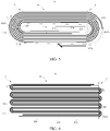
- FIG. 5 is a schematic structural diagram of an electrode assembly 22 according to some embodiments of this application; and FIG. 6 is a schematic structural diagram of an electrode assembly 22 according to other embodiments of this application.
- the electrode assembly 22 includes a negative electrode plate 221 and a positive electrode plate 222.
- the negative electrode plate 221 and the positive electrode plate 222 are wound or folded to form a bend region A.
- the positive electrode plate 222 includes a plurality of bend portions 2220 located in the bend region A.
- Each bend portion 2220 includes a positive current collecting layer 2220a (not shown in FIG. 5 or FIG. 6 ) and a positive active material layer 2220b (not shown in FIG. 5 or FIG. 6 ).
- the positive current collecting layer 2220a is coated with the positive active material layer 2220b on at least one side in a thickness direction of the positive electrode plate 222.
- a barrier layer 223 is disposed between the positive current collecting layer 2220a and the positive active material layer 2220b. The barrier layer 223 is configured to prevent electron transport between the positive current collecting layer 2220a and the positive active material layer 2220b.
- the barrier layer 223 is disposed between the positive current collecting layer 2220a and the positive active material layer 2220b of the bend portion 2220.
- the barrier layer 223 can prevent electron transport between the positive current collecting layer 2220a and the positive active material layer 2220b, so as to weaken or preclude delithiation reactions of the positive active material layer 2220b of the positive electrode plate 222 at the bend portion 2220. Even if a negative active material falls off from the bend portion 2220 of the negative electrode plate 221, because no lithium ions or just a small quantity of lithium ions need to be intercalated, the probability of lithium plating is reduced, or occurrence of lithium plating is avoided, thereby improving battery safety.
- the positive active material layer 2220b cannot release ions until electron transport occurs on an interface between the positive current collecting layer 2220a and the positive active material layer 2220b.
- the barrier layer 223 prevents the electron transport between the positive current collecting layer 2220a and the positive active material layer 2220b. Therefore, the barrier layer 223 actually serves to prevent the positive active material layer 2220b from releasing ions.
- the ions released by particles in the positive active material layer 2220b are lithium ions. That is, the barrier layer 223 serves to prevent the particles from releasing lithium ions.
- the positive electrode plate 222 and the negative electrode plate 221 may be stacked first and then wound to form a jelly-roll structure that includes a bend region A, for example, a flat jelly-roll structure.
- the positive electrode plate 222 and the negative electrode plate 221 may be stacked first and then bent to form a folded structure that includes a bend region A.
- the positive electrode plate 222 and the negative electrode plate 221 are stacked and then folded back and forth in an S shape to form a folded structure.
- the electrode assembly 22 may further include a separator 224.
- the separator 224 is configured to separate the positive electrode plate 222 from the negative electrode plate 221 to reduce risks of short circuits between the positive electrode plate 222 and the negative electrode plate 221.
- the separator 224 may be made of a material such as PP (polypropylene, polypropylene) or PE (polyethylene, polyethylene).
- the electrode plates and separator may be stacked sequentially in order from the positive electrode plate 222 to the separator 224, the negative electrode plate 221, and then the separator 224, and then the four items are wound to form a jelly-roll structure.
- the electrode assembly 22 is folded structure, the items may be stacked sequentially in order from the separator 224 to the positive electrode plate 222, the separator 224, the negative electrode plate 221, and then the separator 224, and then the five items are folded to form a folded structure.
- the electrode assembly 22 may further include a straight region B.
- the straight region B is connected to the bend region A.
- the bend region A may be disposed at both opposite ends of the straight region B.
- the straight region B is a straight-structured region of the electrode assembly 22.
- a part that is of the positive electrode plate 222 and that is located in the straight region B and a part that is of the negative electrode plate 221 and that is located in the straight region B are both arranged in a flat and straight manner approximately.
- the two bend regions A are located at two ends of the straight region B respectively.
- the bend region A is a bend-structured region of the jelly-roll structure.
- a part that is of the positive electrode plate 222 and that is located in the bend region A (the part forms the bend portion 2220) and a part that is of the negative electrode plate 221 and that is located in the bend region A are both arranged in a bent manner.
- the part that is of the positive electrode plate 222 and that is located in the bend region A (the part forms the bend portion 2220) and the part that is of the negative electrode plate 221 and that is located in the bend region A are both arc-shaped.
- both ends of the barrier layer 223 extending along a bending direction C of the bend portion 2220 are located in the bend region A. That is, the entire barrier layer 223 is located in the bend region A, thereby alleviating or avoiding an impact caused by the barrier layer 223 to a part that is of the positive electrode plate 222 and that is located outside the bend region A.
- the bending direction C of the bend portion 2220 is a circumferential direction of an arc on which the bend portion 2220 is located. For example, as shown in FIG. 6 , both ends of the barrier layer 223 extending along the bending direction C of the bend portion 2220 are located at a boundary between the bend region A and the straight region B.
- FIG. 8 is a partial view of a part that is of an electrode assembly and that is located in a bend region according to some embodiments of this application. Both ends of the barrier layer 223 extending along the bending direction C of the bend portion 2220 are located in the bend region A, and one end or both ends of the barrier layer 223 are spaced apart from the boundary between the straight region B and the bend region A. For example, as shown in FIG. 8 , neither end of the barrier layer 223 extends to the boundary between the straight region B and the bend region A. The barrier layer 223 is not disposed in a partial section at the two ends of the bend portion 2220.
- electrons can be transported between the positive current collecting layer 2220a and the positive active material layer 2220b, and the positive active material layer 2220b may release lithium ions.
- the barrier layer 223 can prevent some electrons from being transported between the positive current collecting layer 2220a and the positive active material layer 2220b, so as to reduce the occurrence of lithium plating, and at the same time, can ensure a relatively high energy density of the electrode assembly.
- both ends of the barrier layer 223 extending along the bending direction C of the bend portion 2220 are located in the straight region B.
- one end of the barrier layer 223 extending along the bending direction C of the bend portion 2220 is located in the straight region B, and the other end is located in the bend region A.
- FIG. 7 is a partial enlarged view of an electrode assembly 22 according to some embodiments of this application.
- the positive electrode plate 222 includes a positive current collector 2221 and a positive active material body 2222 coated on both sides of the positive current collector 2221 in the thickness direction.
- the positive current collector 2221 may include a part that is not coated with the positive active material body 2222. This part may serve as a positive tab, and may be used for electrical connection to the positive electrode terminal 23 (referring to FIG. 4 ).
- the negative electrode plate 221 may include a negative current collector 2211 and a negative active material body 2212 coated on both sides of the negative current collector 2211 in the thickness direction.
- the negative current collector 2211 may include a part that is not coated with the negative active material body 2212. This part may serve as a negative tab, and may be used for electrical connection to the negative electrode terminal 24 (referring to FIG. 4 ).
- the positive current collecting layer 2220a of the bend portion 2220 is the part that is of the positive current collector 2221 and that is located in the bend region A.
- the positive active material layer 2220b of the bend portion 2220 is the part that is of the positive active material body 2222 and that is located in the bend region A.
- the positive active material layer 2220b may be coated on an inner side 2220c of the positive current collecting layer 2220a, or the positive active material layer 2220b may be coated on an outer side 2220d of the positive current collecting layer 2220a, or the positive active material layer 2220b may be coated on both the outer side 2220d and the inner side 2220c of the positive current collecting layer 2220a.
- the inner side 2220c of the positive current collecting layer 2220a is located inside against the outer side 2220d.
- the inner side 2220c of the positive current collecting layer 2220a is closer to the straight region B than the outer side 2220d.
- FIG. 8 is a partial enlarged view of an electrode assembly 22 according to some embodiments of this application.
- One surface of the barrier layer 223 is attached to the positive current collecting layer 2220a, and the other surface is attached to the positive active material layer 2220b.
- Attaching means bonding or coating or spraying.
- the barrier layer 223 is firmly connected to the positive current collecting layer 2220a and the positive active material layer 2220b by attaching, thereby alleviating or avoiding dislocation of the barrier layer 223 during use of the battery cell 20.
- the arrangement of the barrier layer 223 is described in detail by using an example in which the electrode assembly 22 is a jelly-roll structure.
- FIG. 8 is a partial view of a part that is of an electrode assembly 22 and that is located in a bend region A according to some embodiments of this application.
- the positive active material layer 2220b is coated on the inner side 2220c of the positive current collecting layer 2220a in the thickness direction of the positive electrode plate 222.
- the barrier layer 223 is disposed between the positive active material layer 2220b located on the inner side 2220c and the positive current collecting layer 2220a in at least one bend portion 2220.
- the barrier layer 223 can prevent at least a part of particles in the positive active material layer 2220b on the inner side 2220c of the positive current collecting layer 2220a from releasing lithium ions to the negative electrode plate 221, thereby alleviating the lithium plating of the negative electrode plate 221 occurring at a section located inside against the barrier layer 223 in the bend region A.
- the thickness direction of the positive electrode plate 222 is also the thickness direction of the positive current collecting layer 2220a.
- the outer side 2220d of the positive current collecting layer 2220a may be coated with the positive active material layer 2220b, or coated with no positive active material layer 2220b.
- the positive active material layer 2220b is coated on both the outer side 2220d and the inner side 2220c of the positive current collecting layer 2220a.
- the barrier layer 223 may be disposed between the positive active material layer 2220b located on the inner side 2220c and the positive current collecting layer 2220a in just one bend portion 2220; or, the barrier layer 223 may be disposed between the positive active material layer 2220b located on the inner side 2220c and the positive current collecting layer 2220a in a plurality of bend portions 2220.
- the positive active material layer 2220b of the bend portion 2220 includes a third part connected to the positive current collecting layer 2220a and a fourth part corresponding to the barrier layer 223.
- a thickness of the fourth part may be the same as a thickness of the third part. In this way, during manufacturing of the positive active material layer 2220b, the thickness is basically the same between all parts of the positive active material layer 2220b, thereby simplifying the manufacturing process. Alternatively, the thickness of the fourth part is smaller than the thickness of the third part.
- a sum of the thickness of the fourth part and the thickness of the barrier layer 223 is equal to the thickness of the third part.
- the thicknesses of all parts of the bend portion 2220 along the bending direction C are close or basically equal to each other, and force distribution is relatively even between the parts.
- FIG. 9 is a partial view of a part that is of an electrode assembly 22 and that is located in a bend region A according to other embodiments of this application.
- the positive active material layer 2220b is coated on the outer side 2220d of the positive current collecting layer 2220a in the thickness direction of the positive electrode plate 222.
- the barrier layer 223 is disposed between the positive active material layer 2220b located on the outer side 2220d and the positive current collecting layer 2220a in at least one bend portion 2220.
- the barrier layer 223 can prevent electron transport between the positive current collecting layer 2220a and the positive active material layer 2220b on the inner side 2220c of the positive current collecting layer, and alleviate lithium plating of a negative active material layer of the negative electrode plate 221 on the outer side 2220d.
- the inner side 2220c of the positive current collecting layer 2220a may be coated with the positive active material layer 2220b, or coated with no positive active material layer 2220b.
- the positive active material layer 2220b is coated on both the outer side 2220d and the inner side 2220c of the positive current collecting layer 2220a.
- the barrier layer 223 may be disposed between the positive active material layer 2220b located on the inner side 2220c and the positive current collecting layer 2220a in just one bend portion 2220; or, the barrier layer 223 may be disposed between the positive active material layer 2220b located on the inner side 2220c and the positive current collecting layer 2220a in a plurality of bend portions 2220.
- FIG. 10 is a partial view of a part that is of an electrode assembly 22 and that is located in a bend region A according to still other embodiments of this application.
- the positive active material layer 2220b is coated on both the outer side 2220d and the inner side 2220c of the positive current collecting layer 2220a.
- the barrier layer 223 is disposed between the positive active material layer 2220b located on the inner side 2220c and the positive current collecting layer 2220a, and between the positive active material layer 2220b located on the outer side 2220d and the positive current collecting layer 2220a, in at least one bend portion 2220.
- the barrier layer 223 can prevent electron transport between the positive active material layer 2220b located on the outer side 2220d of the positive current collecting layer 2220a and the positive current collecting layer 2220a, and prevent electron transport between the positive active material layer 2220b located on the inner side 2220c of the positive current collecting layer 2220a and the positive current collecting layer 2220a, thereby alleviating lithium plating of the negative active material layer on both the inner side and the outer side 2220d in the negative electrode plate 221.
- the barrier layer 223 is disposed for both the positive active material layer 2220b on the inner side and the positive electrode active material layer 2220b on the outer side in at least one bend portion 2220.
- the barrier layer 223 may be disposed in all the bend portions 2220 in the bend region A, or the barrier layer 223 may be disposed in a part of the bend portions 2220 in the bend region A.
- the barrier layer 223 is disposed in one, two, or three innermost bend portions 2220 in the bend region A.
- FIG. 11 is a partial view of the electrode assembly 22 shown in FIG. 5 .
- the innermost electrode plate in the bend region A is a negative electrode plate 221.
- the barrier layer 223 is disposed in the innermost bend portion 2220 of the bend region A.
- the innermost electrode plate in the bend region A is a negative electrode plate 221.
- a section that is of the negative electrode plate 221 and that is closer to the inside in the bend region is bent to a greater extent, incurs severer detachment of coating than other sections, and is more prone to lithium plating than other sections. Therefore, the barrier layer 223 is disposed in the innermost bend portion 2220 of the bend region A to alleviate lithium plating effectively.
- the barrier layer 223 may be disposed between the positive active material layer 2220b located on the inner side 2220c and the positive current collecting layer 2220a in an innermost bend portion 2220 of the bend region A; or, the barrier layer 223 may be disposed between the positive active material layer 2220b located on the outer side 2220d and the positive current collecting layer 2220a in the innermost bend portion 2220 of the bend region A; or, the barrier layer 223 may be disposed between the positive active material layer 2220b located on the inner side 2220c and the positive current collecting layer 2220a in an innermost bend portion 2220 of the bend region A, and between the positive active material layer 2220b located on the outer side 2220d and the positive current collecting layer 2220a in the innermost bend portion 2220 of the bend region A.
- one end or two ends of the barrier layer 223 extending along a first direction do not exceed the positive active material layer 2220b, the first direction being perpendicular to a bending direction C of the bend region A.
- a section not covered by the barrier layer 223 exists at one end or two ends of the bend portion 2220 along a direction perpendicular to the bending direction C. Therefore, some electrons are prevented from being transported between the positive current collecting layer 2220a and the positive active material layer 2220b, so as to reduce the occurrence of lithium plating. At the same time, a relatively high energy density of the electrode assembly is ensured.
- FIG. 12 is a partial view of a part that is of an electrode assembly and that is located in a bend region A according to still other embodiments of this application.
- the plurality of barrier layers 223 are spaced out along the bending direction C of the bend region A, or the plurality of the barrier layers 223 are spaced out along a first direction.
- the first direction is perpendicular to the bending direction C of the bend region A.
- the plurality of barrier layers 223 are disposed discretely. Adjacent barrier layers 223 are spaced out by a given distance along the bending direction C of the bend region A or the first direction. A section not covered by the barrier layer 223 exists at the bend portion 2220. In this way, some electrons are prevented from being transported between the positive current collecting layer 2220a and the positive active material layer 2220b, so as to reduce the occurrence of lithium plating. At the same time, a relatively high energy density of the electrode assembly is ensured.
- FIG. 12 as an example, there are a plurality of discrete barrier layers 223. The plurality of barrier layers 223 are spaced out along the bending direction C of the bend region A.
- the plurality of barrier layers 223 may be all located in the bend region A.
- a part of the barrier layers 223 at one end or both ends in the bending direction C of the bend region A among the plurality of barrier layers 223 may extend to the straight region B, and remaining barrier layers 223 are located in the bend region A.
- the plurality of barrier layers 223 may be all located in the bend region A.
- a part of the barrier layers 223 at one end or both ends in the first direction among the plurality of barrier layers 223 may extend to the straight region B, and remaining barrier layers 223 are located in the bend region A.
- the barrier layer 223 is an insulation layer. Due to a relatively high resistance, the insulation layer can prevent transport of some electrons between the positive current collecting layer 2220a and the positive active material layer 2220b, thereby reducing occurrence of lithium plating.
- the barrier layer 223 includes at least one of an insulation adhesive layer, a ceramic insulation layer, or insulation tape.
- an insulation adhesive layer e.g., a combination of one or more of the insulation adhesive layer, the ceramic insulation layer, or the insulation tape is used as the barrier layer 223, all of which can effectively prevent electron transport between the positive current collecting layer 2220a and the positive active material layer 2220b, thereby reducing occurrence of lithium plating.
- constituents of the insulation adhesive layer include at least one of styrene-butadiene rubber, polyacrylate, polyvinyl chloride, polyvinylidene difluoride, poly(vinylidene fluoride-co-hexafluoropropylene), epoxy resin, poly(butadiene-co-acrylonitrile), polyurethane rubber, polymethyl acrylate, or polyethyl acrylate.
- the insulation adhesive layer made of the foregoing constituents can effectively prevent electron transport between the positive current collecting layer 2220a and the positive active material layer 2220b, thereby reducing occurrence of lithium plating.
- two surfaces of the insulation adhesive layer are bonded to the positive current collecting layer 2220a and the positive active material layer 2220b respectively.
- the two surfaces of the insulation adhesive layer are adhesive, and are bonded to the positive current collecting layer 2220a and the positive active material layer 2220b respectively to alleviate or avoid dislocation of the insulation adhesive layer during use of the battery cell 20.
- constituents of the insulation adhesive layer further include a colorant.
- the insulation adhesive layer differs from the positive current collecting layer 2220a in at least one of pixel distribution, brightness, color, or the like.
- the position of the insulation adhesive layer of the positive electrode plate 222 can be determined by using a visual inspection device.
- the position of the insulation adhesive layer is a position at which the bend region A is formed. After the position of the insulation adhesive layer is determined, it is convenient to determine a starting position of winding.
- the ceramic insulation layer is a mixture of ceramic particles and a polymer binder.
- the ceramic particles include at least one of aluminum oxide, titanium oxide, barium sulfate, or zirconium oxide.
- Constituents of the polymer binder include at least one of styrene-butadiene rubber, polyacrylate, polyvinyl chloride, polyvinylidene difluoride, poly(vinylidene fluoride-co-hexafluoropropylene), epoxy resin, poly(butadiene-co-acrylonitrile), polyurethane rubber, polymethyl acrylate, or polyethyl acrylate.
- the polymer binder can be bonded to the positive current collecting layer 2220a and the positive active material layer 2220b.
- the ceramic particles can prevent electron transport between the positive current collecting layer 2220a and the positive active material layer 2220b, thereby reducing occurrence of lithium plating.
- a substrate material of the insulation tape is polyethylene terephthalate, polyvinyl chloride, polyethylene, or oriented polypropylene.
- the insulation tape made of the foregoing material can prevent electron transport between the positive current collecting layer 2220a and the positive active material layer 2220b, thereby reducing occurrence of lithium plating.
- FIG. 13 is a flowchart of a method for manufacturing an electrode assembly 22 according to some embodiments of this application.
- the method for manufacturing an electrode assembly 22 includes the following steps:
- the positive electrode plate 222 includes a plurality of bend portions 2220 located in the bend region A.
- Each bend portion 2220 includes a positive current collecting layer 2220a and a positive active material layer 2220b.
- the positive current collecting layer 2220a is coated with the positive active material layer 2220b on at least one surface in a thickness direction of the positive electrode plate 222.
- a barrier layer 223 is disposed between the positive current collecting layer 2220a and the positive active material layer 2220b.
- the barrier layer 223 is configured to prevent electron transport between the positive current collecting layer 2220a and the positive active material layer 2220b.
- FIG. 14 is a flowchart of a method for manufacturing an electrode assembly 22 according to other embodiments of this application.
- the method for manufacturing an electrode assembly 22 further includes the following step: S150: Dispose the barrier layer 223 between the positive current collecting layer 2220a on at least one surface of the positive electrode plate in the thickness direction of the positive electrode plate 222 and the positive active material layer 2220b before winding or folding the positive electrode plate 222 and the negative electrode plate 221.
- the barrier layer 223 is an insulation adhesive layer
- the material of the insulation adhesive layer may be coated on the positive active material layer 2220b of the positive electrode plate 222 first, and is cured to obtain an insulation adhesive layer. Subsequently, the positive electrode plate 222 and the negative electrode plate 221 are wound or folded.
- FIG. 15 is a flowchart of a method for manufacturing an electrode assembly 22 according to still other embodiments of this application.
- the method includes: providing a separator 224 configured to separate the positive electrode plate 222 from the negative electrode plate 221, winding or folding the positive electrode plate 222, the separator 224, and the negative electrode plate 221 to form the bend region A.
- FIG. 16 is a schematic block diagram of a device 2000 for manufacturing an electrode assembly 22 according to some embodiments of this application.
- the manufacturing device 2000 includes: a first providing device 1100, a second providing device 1200, a third providing device 1300, and an assembling device 1400.
- the first providing device 1100 is configured to provide a positive electrode plate 222.
- the second providing device 1200 is configured to provide a negative electrode plate 221.
- the third providing device 1300 is configured to provide a barrier layer 223.
- the assembling device 1400 is configured to wind or fold the positive electrode plate 222 and the negative electrode plate 221 to form a bend region A.
- the positive electrode plate 222 includes a plurality of bend portions 2220 located in the bend region A.
- Each bend portion 2220 includes a positive current collecting layer 2220a and a positive active material layer 2220b.
- the positive current collecting layer 2220a is coated with the positive active material layer 2220b on at least one surface in a thickness direction of the positive electrode plate 222.
- a barrier layer 223 is disposed between the positive current collecting layer 2220a and the positive active material layer 2220b.
- the barrier layer 223 is configured to prevent electron transport between the positive current collecting layer 2220a and the positive active material layer 2220b.
- the manufacturing device 2000 further includes a fourth providing device (not shown in the drawing).
- the fourth providing device is configured to provide a separator 224 that separates the positive electrode plate 222 from the negative electrode plate 221.
- the assembling device 1400 is configured to wind or fold the positive electrode plate 222, the separator 224, and the negative electrode plate 221 to form a bend region A.
Landscapes
- Chemical & Material Sciences (AREA)
- Chemical Kinetics & Catalysis (AREA)
- Electrochemistry (AREA)
- General Chemical & Material Sciences (AREA)
- Engineering & Computer Science (AREA)
- Manufacturing & Machinery (AREA)
- Materials Engineering (AREA)
- Composite Materials (AREA)
- Battery Electrode And Active Subsutance (AREA)
- Secondary Cells (AREA)
Abstract
Description
- This application relates to the field of batteries, and in particular, to an electrode assembly, a battery cell, a battery, and a method and device for manufacturing an electrode assembly.
- With the rapid development of smartphones, tablet computers, and electric vehicles, lithium-ion batteries are used more widely, and accordingly, higher requirements are posed on the lithium batteries. People expect higher electrical performance of a lithium battery in addition to safety performance of the battery. Lithium plating is one of main factors affecting the electrical performance and safety performance of the battery. Once lithium plating occurs in the battery, not only the electrical performance of the battery will deteriorate, but also dendrites are prone to take shape with the accumulation of lithium precipitated. The dendrites are prone to puncture the separator, cause an internal short circuit in the battery, and result in a safety hazard.
- Therefore, how to effectively avoid or reduce the risks of lithium plating in the battery has become an urgent technical problem currently.
- This application provides an electrode assembly, a battery cell, a battery, and a manufacturing method and device to alleviate or avoid lithium plating and improve battery safety.
- According to a first aspect, an embodiment of this application provides an electrode assembly, including: a positive electrode plate and a negative electrode plate. The positive electrode plate and the negative electrode plate are wound or folded to form a bend region.
- The positive electrode plate includes a plurality of bend portions located in the bend region. Each bend portion includes a positive current collecting layer and a positive active material layer. The positive current collecting layer is coated with the positive active material layer on at least one surface in a thickness direction of the positive electrode plate.
- A barrier layer is disposed between the positive current collecting layer and the positive active material layer. The barrier layer is configured to prevent electron transport between the positive current collecting layer and the positive active material layer.
- In the foregoing technical solution, the barrier layer is disposed between the positive current collecting layer and the positive active material layer of the bend portion. The barrier layer can prevent electron transport between the positive current collecting layer and the positive active material layer, thereby weakening or precluding delithiation reactions of the positive active material layer of the positive electrode plate at the bend portion. Even if a negative active material falls off from the bend portion of the negative electrode plate, because no lithium ions or just a small quantity of lithium ions need to be intercalated, the probability of lithium plating is reduced, or occurrence of lithium plating is avoided, thereby improving battery safety.
- In some embodiments, the positive current collecting layer is coated with the positive active material layer on an inner side of the positive current collecting layer in the thickness direction. The barrier layer is disposed between the positive active material layer located on the inner side and the positive current collecting layer in at least one bend portion.
- In the foregoing technical solution, the barrier layer is disposed between the positive active material layer located on the inner side and the positive current collecting layer in at least one bend portion. The barrier layer can prevent electron transport between the positive current collecting layer and the positive active material layer located on the inner side of the positive current collecting layer, and alleviate lithium plating of a negative active material layer on an outer side in the negative electrode plate.
- In some embodiments, the positive active material layer is coated on the outer side of the positive current collecting layer in the thickness direction. The barrier layer is disposed between the positive active material layer located on the outer side and the positive current collecting layer in at least one bend portion.
- In the foregoing technical solution, the barrier layer is disposed between the positive active material layer located on the outer side and the positive current collecting layer in at least one bend portion. The barrier layer can prevent electron transport between the positive current collecting layer and the positive active material layer on the outer side of the positive current collecting layer, and alleviate lithium plating of the negative active material layer of the negative electrode plate on the inner side.
- In some embodiments, the positive current collecting layer is coated with the positive active material layer on both the inner side and the outer side in the thickness direction. The barrier layer is disposed between the positive active material layer located on the inner side and the positive current collecting layer, and between the positive active material layer located on the outer side and the positive current collecting layer, in at least one bend portion.
- In the foregoing technical solution, the barrier layer is disposed between the positive active material layer located on the inner side and the positive current collecting layer, and between the positive active material layer located on the outer side and the positive current collecting layer, in at least one bend portion. The barrier layer can prevent electron transport between the positive active material layer located on the outer side of the positive current collecting layer and the positive current collecting layer, and prevent electron transport between the positive active material layer located on the inner side of the positive current collecting layer and the positive current collecting layer, thereby alleviating lithium plating of the negative active material layer on both the inner side and the outer side in the negative electrode plate.
- In some embodiments, the positive electrode plate and the negative electrode plate are wound to form a jelly-roll structure. The jelly-roll structure includes a bend region.
- An innermost electrode plate in the bend region is a negative electrode plate, and the barrier layer is disposed in an innermost bend portion of the bend region.
- At a section closer to the inside, the section of the negative electrode plate in the bend region is bent to a greater extent, and detachment of coating is severer than other sections, and lithium plating is more likely to occur. In the foregoing technical solution, the barrier layer is disposed in the innermost bend portion of the bend region. The barrier layer can prevent transport of at least a part of electrons between the innermost positive current collecting layer and the positive active material layer, and reduce occurrence of the lithium plating at the inner part of the negative electrode plate in the bend region.
- In some embodiments, both ends of the barrier layer extending along a bending direction of the bend portion are located in the bend region.
- In the foregoing technical solution, the entire barrier layer is located in the bend region, thereby alleviating or avoiding an impact caused by the barrier layer to a part that is of the positive electrode plate and that is located outside the bend region.
- In some embodiments, the electrode assembly includes a straight region connected to the bend region.
- Both ends of the barrier layer extending along a bending direction of the bend portion are located in the straight region, or, one end of the barrier layer extending along a bending direction of the bend portion is located in the straight region, and the other end is located in the bend region.
- In the foregoing technical solution, a relatively large quantity of electrons can be prevented from being transported between the positive current collecting layer and the positive active material layer, thereby reducing occurrence of lithium plating.
- In some embodiments, one end or two ends of the barrier layer extending along a first direction do not exceed the positive active material layer, the first direction being perpendicular to a bending direction of the bend region.
- In the foregoing technical solution, some electrons can be prevented from being transported between the positive current collecting layer and the positive active material layer, and the occurrence of lithium plating is reduced. At the same time, a relatively high energy density of the electrode assembly is ensured.
- In some embodiments, there are a plurality of discrete barrier layers. The plurality of barrier layers are spaced out along a bending direction of the bend region, or the plurality of the barrier layers are spaced out along a first direction. The first direction is perpendicular to the bending direction of the bend region.
- In the foregoing technical solution, some electrons can be prevented from being transported between the positive current collecting layer and the positive active material layer, and the occurrence of lithium plating is reduced. At the same time, a relatively high energy density of the electrode assembly is ensured.
- In some embodiments, one surface of the barrier layer is attached to the positive current collecting layer, and the other surface is attached to the positive active material layer.
- In the foregoing technical solution, the barrier layer is firmly connected to the positive current collecting layer and the positive active material layer to alleviate or avoid dislocation of the barrier layer during use of the battery cell.
- In some embodiments, the barrier layer is an insulation layer.
- In the foregoing technical solution, due to a relatively high resistance, the insulation layer can thoroughly prevent electron transport between the positive current collecting layer and the positive active material layer, thereby reducing occurrence of lithium plating.
- In some embodiments, the barrier layer includes at least one of an insulation adhesive layer, a ceramic insulation layer, or insulation tape.
- In the foregoing technical solution, a combination of one or more of the insulation adhesive layer, the ceramic insulation layer, or the insulation tape can effectively prevent electron transport between the positive current collecting layer and the positive active material layer, thereby reducing occurrence of lithium plating.
- In some embodiments, constituents of the insulation adhesive layer include at least one of styrene-butadiene rubber, polyacrylate, polyvinyl chloride, polyvinylidene difluoride, poly(vinylidene fluoride-co-hexafluoropropylene), epoxy resin, poly(butadiene-co-acrylonitrile), polyurethane rubber, polymethyl acrylate, or polyethyl acrylate.
- In the foregoing technical solution, the insulation adhesive layer made of the foregoing constituents can effectively prevent electron transport between the positive current collecting layer and the positive active material layer, thereby reducing occurrence of lithium plating.
- In some embodiments, two surfaces of the insulation adhesive layer are bonded to the positive current collecting layer and the positive active material layer respectively.
- In the foregoing technical solution, the insulation adhesive layer is firmly connected to the positive current collecting layer and the positive active material layer to alleviate or avoid dislocation of the insulation adhesive layer during use of the battery cell.
- In some embodiments, the ceramic insulation layer is a mixture of ceramic particles and a polymer binder. The ceramic particles include at least one of aluminum oxide, titanium oxide, barium sulfate, or zirconium oxide.
- Constituents of the polymer binder include at least one of styrene-butadiene rubber, polyacrylate, polyvinyl chloride, polyvinylidene difluoride, poly(vinylidene fluoride-co-hexafluoropropylene), epoxy resin, poly(butadiene-co-acrylonitrile), polyurethane rubber, polymethyl acrylate, or polyethyl acrylate.
- In the foregoing technical solution, the polymer binder can be bonded to the positive current collecting layer and the positive active material layer. The ceramic particles can prevent electron transport between the positive current collecting layer and the positive active material layer, thereby reducing occurrence of lithium plating.
- In some embodiments, a substrate material of the insulation tape is polyethylene terephthalate, polyvinyl chloride, polyethylene, or oriented polypropylene.
- The insulation tape made of the foregoing material can prevent electron transport between the positive current collecting layer and the positive active material layer, thereby reducing occurrence of lithium plating.
- According to a second aspect, an embodiment of this application provides a battery cell. The battery cell includes a shell and the electrode assembly described above.
- The electrode assembly is accommodated in the shell.
- According to a third aspect, an embodiment of this application provides a battery, including a box and the battery cell described above.
- The battery cell is accommodated in the box.
- According to a fourth aspect, an embodiment of this application provides an electrical device, including the battery described above.
- According to a fifth aspect, an embodiment of this application provides a method for manufacturing an electrode assembly. The manufacturing method includes:
- providing a positive electrode plate, a negative electrode plate, and a barrier layer; and
- winding or folding the positive electrode plate and the negative electrode plate to form a bend region.
- The positive electrode plate includes a plurality of bend portions located in the bend region. Each bend portion includes a positive current collecting layer and a positive active material layer. The positive current collecting layer is coated with the positive active material layer on at least one surface in a thickness direction of the positive electrode plate.
- A barrier layer is disposed between the positive current collecting layer and the positive active material layer. The barrier layer is configured to prevent electron transport between the positive current collecting layer and the positive active material layer.
- In some embodiments, the manufacturing method further includes:
disposing the barrier layer between the positive current collecting layer on at least one surface of the positive electrode plate in the thickness direction of the positive electrode plate and the positive active material layer before winding or folding the positive electrode plate and the negative electrode plate. - In some embodiments, the method further includes: providing a separator configured to separate the positive electrode plate from the negative electrode plate, and winding or folding the positive electrode plate, the separator, and the negative electrode plate to form the bend region.
- According to a sixth aspect, an embodiment of this application provides a device for manufacturing an electrode assembly, including:
- a first providing device, configured to provide a positive electrode plate;
- a second providing device, configured to provide a negative electrode plate; and
- a third providing device, configured to provide a barrier layer; and
- an assembling device, configured to wind or fold the positive electrode plate and the negative electrode plate to form a bend region.
- The positive electrode plate includes a plurality of bend portions located in the bend region. Each bend portion includes a positive current collecting layer and a positive active material layer. The positive current collecting layer is coated with the positive active material layer on at least one surface in a thickness direction of the positive electrode plate.
- A barrier layer is disposed between the positive current collecting layer and the positive active material layer. The barrier layer is configured to prevent electron transport between the positive current collecting layer and the positive active material layer.
- To describe the technical solutions in the embodiments of this application more clearly, the following outlines the drawings used in the embodiments of this application. Evidently, the drawings outlined below are merely a part of embodiments of this application. A person of ordinary skill in the art may derive other drawings from the outlined drawings without making any creative efforts.
-
FIG. 1 is a schematic structural diagram of a vehicle according to some embodiments of this application; -
FIG. 2 is an exploded view of a battery according to some embodiments of this application; -
FIG. 3 is a schematic structural diagram of a battery module shown inFIG. 2 ; -
FIG. 4 is an exploded view of a battery cell shown inFIG. 3 ; -
FIG. 5 is a schematic structural diagram of an electrode assembly according to some embodiments of this application; -
FIG. 6 is a schematic structural diagram of an electrode assembly according to other embodiments of this application; -
FIG. 7 is a partial enlarged view of an electrode assembly according to some embodiments of this application; -
FIG. 8 is a partial view of a part that is of an electrode assembly and that is located in a bend region according to some embodiments of this application; -
FIG. 9 is a partial view of a part that is of an electrode assembly and that is located in a bend region according to other embodiments of this application; -
FIG. 10 is a partial view of a part that is of an electrode assembly and that is located in a bend region according to still other embodiments of this application; -
FIG. 11 is a partial view of the electrode assembly shown inFIG. 5 ; -
FIG. 12 is a partial view of a part that is of an electrode assembly and that is located in a bend region according to still other embodiments of this application; -
FIG. 13 is a flowchart of a method for manufacturing an electrode assembly according to some embodiments of this application; -
FIG. 14 is a flowchart of a method for manufacturing an electrode assembly according to other embodiments of this application; -
FIG. 15 is a flowchart of a method for manufacturing an electrode assembly according to still other embodiments of this application; and -
FIG. 16 is a schematic block diagram of a device for manufacturing an electrode assembly according to some embodiments of this application. - The drawings are not drawn to scale.
- The following gives a more detailed description of implementations of this application with reference to drawings and embodiments. The detailed description of the following embodiments and the accompanying drawings are intended to exemplarily describe the principles of this application, but not to limit the scope of this application. Therefore, this application is not limited to the described embodiments.
- In the description of this application, unless otherwise specified, "a plurality of" means at least two in number; the terms such as "up", "down", "left", "right", "in", and "out" indicating a direction or a position relationship are merely intended for ease or brevity of description of this application, but do not indicate or imply that the mentioned apparatus or component is necessarily located in the specified direction or constructed or operated in the specified direction. Therefore, such terms are not to be understood as a limitation on this application. In addition, the terms "first", "second", and "third" are merely intended for descriptive purposes, but are not intended to indicate or imply relative importance. "Perpendicular" does not means exact perpendicularity, but means perpendicularity falling within an error tolerance range. "Parallel" does not mean exact parallelism, but means parallelism falling within an error tolerance range.
- The directional terms appearing in the following description indicate the directions shown in the drawings, but are not intended to limit specific structures in this application. In the description of this application, unless otherwise expressly specified, the terms "mount", "concatenate", and "connect" are understood in a broad sense. For example, a "connection" may be a fixed connection, a detachable connection, or an integrated connection, and may be a direct connection or an indirect connection implemented through an intermediary. A person of ordinary skill in the art can understand the specific meanings of the terms in this application according to specific situations.
- The term "and/or" in this application indicates merely a relation for describing the related items, and represents three possible relationships. For example, "A and/or B" may represent the following three circumstances: A alone, both A and B, and B alone. In addition, the character "/" herein generally indicates an "or" relationship between the item preceding the character and the item following the character.
- In embodiments of this application, the same reference numeral denotes the same component. For brevity, detailed descriptions of the same component are omitted in a different embodiment. Understandably, dimensions such as thickness, length, and width of various components in the embodiments of this application shown in the drawings, and dimensions such as overall thickness, length, and width of an integrated device are merely exemplary descriptions, but do not constitute any limitation on this application.
- In this application, a battery cell may include a lithium-ion secondary battery, a lithium-ion primary battery, a lithium-sulfur battery, a sodium-lithium-ion battery, a sodium-ion battery, a magnesium-ion battery, or the like. The embodiments of this application do not limit the type of the battery cell. The battery cell may be in a cylindrical shape, a flat shape, a cuboidal shape, or other shapes. The embodiments of this application do not limit the shape of the battery cell. Depending on the form of packaging, the battery cell is typically classed into three types: cylindrical battery cell, prismatic battery cell, and pouch-type battery cell. The embodiments of this application do not limit the form of the battery cell.
- The battery mentioned in the embodiments of this application means a stand-alone physical module that includes one or more battery cells to provide a higher voltage and a higher capacity. For example, the battery mentioned in this application may include a battery module, a battery pack, or the like. A battery typically includes a box configured to package one or more battery cells. The box can prevent liquid or other foreign matters from affecting the charging or discharge of the battery cells.
- A battery cell includes an electrode assembly and an electrolytic solution. The electrode assembly includes a positive electrode plate, a negative electrode plate, and a separator. The battery cell works primarily by relying on movement of metal ions between the positive electrode plate and the negative electrode plate. The positive electrode plate includes a positive current collector and a positive active material body. The positive active material body is coated on a surface of the positive current collector. A part that is of the positive current collector and that is not coated with the positive active material body protrudes from a part that is of the positive current collector and that is coated with the positive active material body. The part that is of the positive current collector and that is not coated with the positive active material body serves as a positive tab. Using a lithium-ion battery as an example, the positive current collector may be made of aluminum, and a positive active material may be lithium cobalt oxide, lithium iron phosphate, ternary lithium, lithium manganese oxide, or the like. The negative electrode plate includes a negative current collector and a negative active material body. The negative active material body is coated on a surface of the negative current collector. A part that is of the negative current collector and that is not coated with the negative active material body protrudes from a part that is of the negative current collector and that is coated with the negative active material body. The part that is of the negative current collector and that is not coated with the negative active material body serves as a negative tab. The negative current collector may be made of copper, and a negative active material may be carbon, silicon, or the like. In order to ensure passage of a large current without fusing off, the positive tab is plural in number, and the plurality of positive tabs are folded together; the negative tab is plural in number, and the plurality of negative tabs are folded together. The separator may be made of a material such as PP (polypropylene, polypropylene) or PE (polyethylene, polyethylene). In addition, the electrode assembly may be a jelly-roll structure or a stacked structure, without being limited herein.
- The development of the battery technology needs to allow for a plurality of design factors, including performance parameters such as energy density, cycle life, discharge capacity, charge rate, and discharge rate, and also needs to ensure safety of the battery.
- For a lithium ion battery, during charging, lithium ions are deintercalated from a positive electrode and intercalated into a negative electrode; and, during discharging, the lithium ions are deintercalated from the negative electrode and intercalated into the positive electrode. During charging of the lithium -ion battery, lithium plating may occur due to abnormal factors such as an insufficient lithiation space of the negative electrode, excessive lithium-ion migration resistance, lithium ions prematurely deintercalated from the positive electrode but unable to be intercalated into the negative electrode in an equal amount. The lithium ions unable to be intercalated into the negative electrode have to gain electrons on a surface of the negative electrode, thereby forming a lithium simple-substance phenomenon, that is, a lithium plating phenomenon.
- The inventor finds that lithium plating is prone to occur at the bend region of the electrode assembly. As found through further research, during winding or folding of the positive electrode plate and the negative electrode plate, detachment of coating is prone to occur at a part of the negative electrode plate in the bend region, resulting in fall-off of a negative active material of the negative electrode plate. Consequently, during charging, a part of the lithium ions deintercalated from the positive electrode plate are unable to be intercalated into the negative electrode plate, resulting in lithium plating.
- In view of this, an embodiment of this application provides a technical solution. A barrier layer is disposed between the positive current collector and the positive active material layer of the positive electrode plate at the bend portion. The barrier layer is configured to prevent electron transport between the positive current collecting layer and the positive active material layer, so as to weaken or preclude delithiation reactions of the positive active material layer at the bend portion. No lithium ions or just a small quantity of lithium ions are deintercalated from the positive active material layer, thereby reducing occurrence of lithium plating and improving safety and service life of the battery cell.
- The technical solutions described in this embodiment of this application are applicable to a battery and an electrical device that uses the battery.
- The electrical device may be a vehicle, a mobile phone, a portable device, a notebook computer, a ship, a spacecraft, an electric toy, a power tool, or the like. The vehicle may be an oil-fueled vehicle, a natural gas vehicle, or a new energy vehicle. The new energy vehicle may be a battery electric vehicle, a hybrid electric vehicle, a range-extended electric vehicle, or the like. The spacecraft includes an airplane, a rocket, a space shuttle, a spaceship, and the like. The electric toy includes a fixed or mobile electric toy, such as a game console, an electric car toy, an electric ship toy, an electric airplane toy, and the like. The power tool includes an electrical metal cutting tool, an electrical grinding tool, an electrical assembling tool, and a power tool for use in railways. Examples of the power tool are an electrical drill, an electrical grinder, an electrical wrench, an electrical screwdriver, an electrical hammer, an electrical impact drill, a concrete vibrator, an electrical planer, and the like. Embodiments of this application do not particularly limit the electrical device.
- For ease of description in the following embodiments, a vehicle is used as an example of the electrical device.
- Referring to
FIG. 1, FIG. 1 is a schematic structural diagram of avehicle 1000 according to some embodiments of this application. Abattery 100 is disposed inside thevehicle 1000. Thebattery 100 may be disposed at the bottom, front, or rear of thevehicle 1000. Thebattery 100 may be configured to supply power to thevehicle 1000. For example, thebattery 100 may serve as an operating power supply of thevehicle 1000. - The
vehicle 1000 may further include acontroller 200 and amotor 300. Thecontroller 200 is configured to control thebattery 100 to supply power to themotor 300, for example, to start or navigate thevehicle 1000, or meet the operating power requirements of the vehicle in operation. - In some embodiments of this application, the
battery 100 serves not only as an operating power supply of thevehicle 1000, but may also serve as a drive power supply of thevehicle 1000 to provide driving power for thevehicle 1000 in place of or partially in place of oil or natural gas. - Referring to
FIG. 2, FIG. 2 is an exploded view of abattery 100 according to some embodiments of this application. Thebattery 100 includes abox 10 and a battery cell 20 (not shown inFIG. 2 ). Thebattery cell 20 is accommodated in thebox 10. - The
box 10 is configured to accommodate thebattery cell 20. Thebox 10 may be one of various structures. In some embodiments, thebox 10 may include afirst part 11 and asecond part 12. Thefirst part 11 and thesecond part 12 fit each other. Thefirst part 11 and thesecond part 12 together define anaccommodation space 13 configured to accommodate thebattery cell 20. Thesecond part 12 may be a hollow structure opened at one end. Thefirst part 11 may be a plate-like structure. Thefirst part 11 fits on an opening side of thesecond part 12 so that thefirst part 11 and thesecond part 12 together define theaccommodation space 13. Alternatively, both thefirst part 11 and thesecond part 12 may be hollow structures opened at one side. The opening side of thefirst part 11 fits the opening side of thesecond part 12. Definitely, thefirst part 11 and thesecond part 12 may be in various shapes, such as a cylinder or a cuboid. - There may be one or
more battery cells 20 in thebattery 100. If there are a plurality ofbattery cells 20, the plurality ofbattery cells 20 may be connected in series, parallel, or series-and-parallel pattern. The series-and-parallel pattern means a combination of series connection and parallel connection of the plurality ofbattery cells 20. The plurality ofbattery cells 20 may be directly connected in series, parallel, or series-and-parallel pattern, and then the whole of the plurality ofbattery cells 20 may be accommodated in thebox 10. Alternatively, the plurality ofbattery cells 20 may be connected in series, parallel, or series-and-parallel pattern to form abattery module 30 first. A plurality ofbattery modules 30 are then connected in series, parallel, or series-and-parallel pattern to form a whole for being accommodated in thebox 10. - In some embodiments, referring to
FIG. 3, FIG. 3 is a schematic structural diagram of abattery module 30 shown inFIG. 2 . Thebattery 100 includes a plurality ofbattery modules 30. Eachbattery module 30 includes a plurality ofbattery cells 20. The plurality ofbattery cells 20 are connected in series, parallel, or series-and-parallel pattern to form thebattery module 30 first. A plurality ofbattery modules 30 are then connected in series, parallel, or series-and-parallel pattern to form a whole for being accommodated in thebox 10. - The plurality of
battery cells 20 in thebattery module 30 may be electrically connected by abusbar component 31, so as to implement parallel connection, series connection, or series-parallel connection between the plurality ofbattery cells 20 in thebattery module 30. - Referring to
FIG. 4, FIG. 4 is an exploded view of thebattery cell 20 shown inFIG. 3 . Thebattery cell 20 according to this embodiment of this application includes ashell 21 and anelectrode assembly 22. Theelectrode assembly 22 is accommodated in theshell 21. - In some embodiments, the
shell 21 may be further configured to accommodate an electrolyte such as an electrolytic solution. Theshell 21 may be one of various structures. - In some embodiments, the
shell 21 may include ahousing 211 and acover 212. Thehousing 211 is a hollow structure opened on one side. Thecover 212 fits on, and is hermetically connected to, the opening of thehousing 211, to form a sealedspace 213 configured to accommodate theelectrode assembly 22 and the electrolyte. - During assembling of the
battery cell 20, theelectrode assembly 22 may be put into thehousing 211 first. Thehousing 211 is filled with an electrolyte, and then thecover 212 fits on the opening of thehousing 211. - The
housing 211 may be in various shapes such as a cylinder or a cuboid. The shape of thehousing 211 may be determined depending on the specific shape of theelectrode assembly 22. For example, if theelectrode assembly 22 is a cylindrical structure, thehousing 211 may be a cylindrical housing. If theelectrode assembly 22 is a cuboidal structure, thehousing 211 may be a cuboidal housing. Also, thecover 212 may be one of various structures. For example, thecover 212 is a plate-like structure, a hollow structure opened at one end, or the like. For example, inFIG. 4 , thehousing 211 is a cuboidal structure, thecover 212 is a plate-like structure, and thecover 212 fits on the opening of thehousing 211. - In some embodiments, the
battery cell 20 may further include apositive electrode terminal 23, anegative electrode terminal 24, and apressure relief mechanism 25. Thepositive electrode terminal 23, thenegative electrode terminal 24, and thepressure relief mechanism 25 are all mounted on thecover 212. Thepositive electrode terminal 23 and thenegative electrode terminal 24 are both configured to electrically connect to theelectrode assembly 22. That is, thepositive electrode terminal 23 is configured to electrically connect to thepositive electrode plate 222, and thenegative electrode terminal 24 is configured to electrically connect to thenegative electrode plate 221. Thepressure relief mechanism 25 is configured to release pressure inside thebattery cell 20 when an internal pressure or temperature of thebattery cell 20 reaches a preset value. - For example, as shown in
FIG. 4 , thepressure relief mechanism 25 is located between thepositive electrode terminal 23 and thenegative electrode terminal 24. Thepressure relief mechanism 25 may be a component such as an explosion-proof valve, a rupture disk, a gas valve, a pressure relief valve, or a safety valve. - Understandably, the
shell 21 is not limited to the structures enumerated above. Theshell 21 may be another structure instead. For example, theshell 21 includes ahousing 211 and twocovers 212. Thehousing 211 is a hollow structure opened on two opposite sides. Onecover 212 fits on, and is hermetically connected to, one corresponding opening of thehousing 211, to form a sealedspace 213 configured to accommodate theelectrode assembly 22 and the electrolyte. In such a structure, thepositive electrode terminal 23 and thenegative electrode terminal 24 may be mounted on thesame cover 212, or may be mounted ondifferent covers 212. Thepressure relief mechanism 25 may be mounted on onecover 212, or thepressure relief mechanism 25 may be mounted on both covers 212. - It needs to be noted that, in this embodiment of this application, one or
more electrode assemblies 22 may be accommodated in theshell 21. For example, inFIG. 4 , there are twoelectrode assemblies 22. - Referring to
FIG. 5 and FIG. 6, FIG. 5 is a schematic structural diagram of anelectrode assembly 22 according to some embodiments of this application; andFIG. 6 is a schematic structural diagram of anelectrode assembly 22 according to other embodiments of this application. Theelectrode assembly 22 includes anegative electrode plate 221 and apositive electrode plate 222. Thenegative electrode plate 221 and thepositive electrode plate 222 are wound or folded to form a bend region A. - The
positive electrode plate 222 includes a plurality ofbend portions 2220 located in the bend region A. Eachbend portion 2220 includes a positivecurrent collecting layer 2220a (not shown inFIG. 5 or FIG. 6 ) and a positiveactive material layer 2220b (not shown inFIG. 5 or FIG. 6 ). The positivecurrent collecting layer 2220a is coated with the positiveactive material layer 2220b on at least one side in a thickness direction of thepositive electrode plate 222. Abarrier layer 223 is disposed between the positivecurrent collecting layer 2220a and the positiveactive material layer 2220b. Thebarrier layer 223 is configured to prevent electron transport between the positivecurrent collecting layer 2220a and the positiveactive material layer 2220b. - The
barrier layer 223 is disposed between the positivecurrent collecting layer 2220a and the positiveactive material layer 2220b of thebend portion 2220. Thebarrier layer 223 can prevent electron transport between the positivecurrent collecting layer 2220a and the positiveactive material layer 2220b, so as to weaken or preclude delithiation reactions of the positiveactive material layer 2220b of thepositive electrode plate 222 at thebend portion 2220. Even if a negative active material falls off from thebend portion 2220 of thenegative electrode plate 221, because no lithium ions or just a small quantity of lithium ions need to be intercalated, the probability of lithium plating is reduced, or occurrence of lithium plating is avoided, thereby improving battery safety. - It needs to be noted that the positive
active material layer 2220b cannot release ions until electron transport occurs on an interface between the positivecurrent collecting layer 2220a and the positiveactive material layer 2220b. Thebarrier layer 223 prevents the electron transport between the positivecurrent collecting layer 2220a and the positiveactive material layer 2220b. Therefore, thebarrier layer 223 actually serves to prevent the positiveactive material layer 2220b from releasing ions. - For example, the ions released by particles in the positive
active material layer 2220b are lithium ions. That is, thebarrier layer 223 serves to prevent the particles from releasing lithium ions. - As shown in
FIG. 5 , thepositive electrode plate 222 and thenegative electrode plate 221 may be stacked first and then wound to form a jelly-roll structure that includes a bend region A, for example, a flat jelly-roll structure. As shown inFIG. 6 , thepositive electrode plate 222 and thenegative electrode plate 221 may be stacked first and then bent to form a folded structure that includes a bend region A. For example, thepositive electrode plate 222 and thenegative electrode plate 221 are stacked and then folded back and forth in an S shape to form a folded structure. - In some embodiments, the
electrode assembly 22 may further include aseparator 224. Theseparator 224 is configured to separate thepositive electrode plate 222 from thenegative electrode plate 221 to reduce risks of short circuits between thepositive electrode plate 222 and thenegative electrode plate 221. - The
separator 224 may be made of a material such as PP (polypropylene, polypropylene) or PE (polyethylene, polyethylene). - If the
electrode assembly 22 is a jelly-roll structure, the electrode plates and separator may be stacked sequentially in order from thepositive electrode plate 222 to theseparator 224, thenegative electrode plate 221, and then theseparator 224, and then the four items are wound to form a jelly-roll structure. If theelectrode assembly 22 is folded structure, the items may be stacked sequentially in order from theseparator 224 to thepositive electrode plate 222, theseparator 224, thenegative electrode plate 221, and then theseparator 224, and then the five items are folded to form a folded structure. - Regardless of whether the
electrode assembly 22 is a jelly-roll structure or a folded structure, theelectrode assembly 22 may further include a straight region B. The straight region B is connected to the bend region A. The bend region A may be disposed at both opposite ends of the straight region B. The straight region B is a straight-structured region of theelectrode assembly 22. A part that is of thepositive electrode plate 222 and that is located in the straight region B and a part that is of thenegative electrode plate 221 and that is located in the straight region B are both arranged in a flat and straight manner approximately. In a direction of extending the part that is of thepositive electrode plate 222 and that is located in the straight region B, the two bend regions A are located at two ends of the straight region B respectively. The bend region A is a bend-structured region of the jelly-roll structure. A part that is of thepositive electrode plate 222 and that is located in the bend region A (the part forms the bend portion 2220) and a part that is of thenegative electrode plate 221 and that is located in the bend region A are both arranged in a bent manner. For example, the part that is of thepositive electrode plate 222 and that is located in the bend region A (the part forms the bend portion 2220) and the part that is of thenegative electrode plate 221 and that is located in the bend region A are both arc-shaped. - In some embodiments, as shown in
FIG. 5 and FIG. 6 , both ends of thebarrier layer 223 extending along a bending direction C of thebend portion 2220 are located in the bend region A. That is, theentire barrier layer 223 is located in the bend region A, thereby alleviating or avoiding an impact caused by thebarrier layer 223 to a part that is of thepositive electrode plate 222 and that is located outside the bend region A. - It needs to be noted that, if one end or both ends of the
barrier layer 223 are just located at a boundary between the straight region B and the bend region A, it is also deemed that thebarrier layer 223 is located in the bend region A. The bending direction C of thebend portion 2220 is a circumferential direction of an arc on which thebend portion 2220 is located. For example, as shown inFIG. 6 , both ends of thebarrier layer 223 extending along the bending direction C of thebend portion 2220 are located at a boundary between the bend region A and the straight region B. - In some embodiments, as shown in
FIG. 8, FIG. 8 is a partial view of a part that is of an electrode assembly and that is located in a bend region according to some embodiments of this application. Both ends of thebarrier layer 223 extending along the bending direction C of thebend portion 2220 are located in the bend region A, and one end or both ends of thebarrier layer 223 are spaced apart from the boundary between the straight region B and the bend region A. For example, as shown inFIG. 8 , neither end of thebarrier layer 223 extends to the boundary between the straight region B and the bend region A. Thebarrier layer 223 is not disposed in a partial section at the two ends of thebend portion 2220. In such a partial section, electrons can be transported between the positivecurrent collecting layer 2220a and the positiveactive material layer 2220b, and the positiveactive material layer 2220b may release lithium ions. In this way, thebarrier layer 223 can prevent some electrons from being transported between the positivecurrent collecting layer 2220a and the positiveactive material layer 2220b, so as to reduce the occurrence of lithium plating, and at the same time, can ensure a relatively high energy density of the electrode assembly. - In other embodiments, both ends of the
barrier layer 223 extending along the bending direction C of thebend portion 2220 are located in the straight region B. In still other embodiments, one end of thebarrier layer 223 extending along the bending direction C of thebend portion 2220 is located in the straight region B, and the other end is located in the bend region A. - In some embodiments, referring to
FIG. 7, FIG. 7 is a partial enlarged view of anelectrode assembly 22 according to some embodiments of this application. Thepositive electrode plate 222 includes a positivecurrent collector 2221 and a positiveactive material body 2222 coated on both sides of the positivecurrent collector 2221 in the thickness direction. The positivecurrent collector 2221 may include a part that is not coated with the positiveactive material body 2222. This part may serve as a positive tab, and may be used for electrical connection to the positive electrode terminal 23 (referring toFIG. 4 ). Thenegative electrode plate 221 may include a negativecurrent collector 2211 and a negativeactive material body 2212 coated on both sides of the negativecurrent collector 2211 in the thickness direction. The negativecurrent collector 2211 may include a part that is not coated with the negativeactive material body 2212. This part may serve as a negative tab, and may be used for electrical connection to the negative electrode terminal 24 (referring toFIG. 4 ). - Understandably, the positive
current collecting layer 2220a of thebend portion 2220 is the part that is of the positivecurrent collector 2221 and that is located in the bend region A. The positiveactive material layer 2220b of thebend portion 2220 is the part that is of the positiveactive material body 2222 and that is located in the bend region A. - In this embodiment of this application, in the
bend portion 2220, the positiveactive material layer 2220b may be coated on aninner side 2220c of the positivecurrent collecting layer 2220a, or the positiveactive material layer 2220b may be coated on anouter side 2220d of the positivecurrent collecting layer 2220a, or the positiveactive material layer 2220b may be coated on both theouter side 2220d and theinner side 2220c of the positivecurrent collecting layer 2220a. In theelectrode assembly 22, as long as thebarrier layer 223 is disposed for one positiveactive material layer 2220b, the occurrence of lithium plating can be reduced effectively. Understandably, theinner side 2220c of the positivecurrent collecting layer 2220a is located inside against theouter side 2220d. Theinner side 2220c of the positivecurrent collecting layer 2220a is closer to the straight region B than theouter side 2220d. - In some embodiments, referring to
FIG. 8, FIG. 8 is a partial enlarged view of anelectrode assembly 22 according to some embodiments of this application. One surface of thebarrier layer 223 is attached to the positivecurrent collecting layer 2220a, and the other surface is attached to the positiveactive material layer 2220b. - Attaching means bonding or coating or spraying. The
barrier layer 223 is firmly connected to the positivecurrent collecting layer 2220a and the positiveactive material layer 2220b by attaching, thereby alleviating or avoiding dislocation of thebarrier layer 223 during use of thebattery cell 20. - For ease of description, in the following embodiments, the arrangement of the
barrier layer 223 is described in detail by using an example in which theelectrode assembly 22 is a jelly-roll structure. - In some embodiments, referring to
FIG. 8, FIG. 8 is a partial view of a part that is of anelectrode assembly 22 and that is located in a bend region A according to some embodiments of this application. The positiveactive material layer 2220b is coated on theinner side 2220c of the positivecurrent collecting layer 2220a in the thickness direction of thepositive electrode plate 222. Thebarrier layer 223 is disposed between the positiveactive material layer 2220b located on theinner side 2220c and the positivecurrent collecting layer 2220a in at least onebend portion 2220. Thebarrier layer 223 can prevent at least a part of particles in the positiveactive material layer 2220b on theinner side 2220c of the positivecurrent collecting layer 2220a from releasing lithium ions to thenegative electrode plate 221, thereby alleviating the lithium plating of thenegative electrode plate 221 occurring at a section located inside against thebarrier layer 223 in the bend region A. - The thickness direction of the
positive electrode plate 222 is also the thickness direction of the positivecurrent collecting layer 2220a. - In this embodiment, the
outer side 2220d of the positivecurrent collecting layer 2220a may be coated with the positiveactive material layer 2220b, or coated with no positiveactive material layer 2220b. InFIG. 8 , as an example, the positiveactive material layer 2220b is coated on both theouter side 2220d and theinner side 2220c of the positivecurrent collecting layer 2220a. Definitely, thebarrier layer 223 may be disposed between the positiveactive material layer 2220b located on theinner side 2220c and the positivecurrent collecting layer 2220a in just onebend portion 2220; or, thebarrier layer 223 may be disposed between the positiveactive material layer 2220b located on theinner side 2220c and the positivecurrent collecting layer 2220a in a plurality ofbend portions 2220. - It needs to be noted that, as shown in
FIG. 8 , the two ends of thebarrier layer 223 are at a distance from the boundary between the straight region B and the bend region A. The positiveactive material layer 2220b of thebend portion 2220 includes a third part connected to the positivecurrent collecting layer 2220a and a fourth part corresponding to thebarrier layer 223. A thickness of the fourth part may be the same as a thickness of the third part. In this way, during manufacturing of the positiveactive material layer 2220b, the thickness is basically the same between all parts of the positiveactive material layer 2220b, thereby simplifying the manufacturing process. Alternatively, the thickness of the fourth part is smaller than the thickness of the third part. For example, a sum of the thickness of the fourth part and the thickness of thebarrier layer 223 is equal to the thickness of the third part. In this way, the thicknesses of all parts of thebend portion 2220 along the bending direction C are close or basically equal to each other, and force distribution is relatively even between the parts. - In some embodiments, referring to
FIG. 9, FIG. 9 is a partial view of a part that is of anelectrode assembly 22 and that is located in a bend region A according to other embodiments of this application. The positiveactive material layer 2220b is coated on theouter side 2220d of the positivecurrent collecting layer 2220a in the thickness direction of thepositive electrode plate 222. Thebarrier layer 223 is disposed between the positiveactive material layer 2220b located on theouter side 2220d and the positivecurrent collecting layer 2220a in at least onebend portion 2220. Thebarrier layer 223 can prevent electron transport between the positivecurrent collecting layer 2220a and the positiveactive material layer 2220b on theinner side 2220c of the positive current collecting layer, and alleviate lithium plating of a negative active material layer of thenegative electrode plate 221 on theouter side 2220d. - In this embodiment, the
inner side 2220c of the positivecurrent collecting layer 2220a may be coated with the positiveactive material layer 2220b, or coated with no positiveactive material layer 2220b. InFIG. 9 , as an example, the positiveactive material layer 2220b is coated on both theouter side 2220d and theinner side 2220c of the positivecurrent collecting layer 2220a. Definitely, thebarrier layer 223 may be disposed between the positiveactive material layer 2220b located on theinner side 2220c and the positivecurrent collecting layer 2220a in just onebend portion 2220; or, thebarrier layer 223 may be disposed between the positiveactive material layer 2220b located on theinner side 2220c and the positivecurrent collecting layer 2220a in a plurality ofbend portions 2220. In some embodiments, referring toFIG. 10, FIG. 10 is a partial view of a part that is of anelectrode assembly 22 and that is located in a bend region A according to still other embodiments of this application. The positiveactive material layer 2220b is coated on both theouter side 2220d and theinner side 2220c of the positivecurrent collecting layer 2220a. Thebarrier layer 223 is disposed between the positiveactive material layer 2220b located on theinner side 2220c and the positivecurrent collecting layer 2220a, and between the positiveactive material layer 2220b located on theouter side 2220d and the positivecurrent collecting layer 2220a, in at least onebend portion 2220. - In this way, the
barrier layer 223 can prevent electron transport between the positiveactive material layer 2220b located on theouter side 2220d of the positivecurrent collecting layer 2220a and the positivecurrent collecting layer 2220a, and prevent electron transport between the positiveactive material layer 2220b located on theinner side 2220c of the positivecurrent collecting layer 2220a and the positivecurrent collecting layer 2220a, thereby alleviating lithium plating of the negative active material layer on both the inner side and theouter side 2220d in thenegative electrode plate 221. InFIG. 10 , as an example, thebarrier layer 223 is disposed for both the positiveactive material layer 2220b on the inner side and the positive electrodeactive material layer 2220b on the outer side in at least onebend portion 2220. - In embodiments of this application, the
barrier layer 223 may be disposed in all thebend portions 2220 in the bend region A, or thebarrier layer 223 may be disposed in a part of thebend portions 2220 in the bend region A. For example, thebarrier layer 223 is disposed in one, two, or threeinnermost bend portions 2220 in the bend region A. - In some embodiments, referring to
FIG. 11, FIG. 11 is a partial view of theelectrode assembly 22 shown inFIG. 5 . Using an example in which thepositive electrode plate 222 and thenegative electrode plate 221 are wound to form a jelly-roll structure that includes a bend region, the innermost electrode plate in the bend region A is anegative electrode plate 221. Thebarrier layer 223 is disposed in theinnermost bend portion 2220 of the bend region A. - The innermost electrode plate in the bend region A is a
negative electrode plate 221. A section that is of thenegative electrode plate 221 and that is closer to the inside in the bend region is bent to a greater extent, incurs severer detachment of coating than other sections, and is more prone to lithium plating than other sections. Therefore, thebarrier layer 223 is disposed in theinnermost bend portion 2220 of the bend region A to alleviate lithium plating effectively. - It needs to be noted that, the
barrier layer 223 may be disposed between the positiveactive material layer 2220b located on theinner side 2220c and the positivecurrent collecting layer 2220a in aninnermost bend portion 2220 of the bend region A; or, thebarrier layer 223 may be disposed between the positiveactive material layer 2220b located on theouter side 2220d and the positivecurrent collecting layer 2220a in theinnermost bend portion 2220 of the bend region A; or, thebarrier layer 223 may be disposed between the positiveactive material layer 2220b located on theinner side 2220c and the positivecurrent collecting layer 2220a in aninnermost bend portion 2220 of the bend region A, and between the positiveactive material layer 2220b located on theouter side 2220d and the positivecurrent collecting layer 2220a in theinnermost bend portion 2220 of the bend region A. - In some embodiments, one end or two ends of the
barrier layer 223 extending along a first direction do not exceed the positiveactive material layer 2220b, the first direction being perpendicular to a bending direction C of the bend region A. - In this way, a section not covered by the
barrier layer 223 exists at one end or two ends of thebend portion 2220 along a direction perpendicular to the bending direction C. Therefore, some electrons are prevented from being transported between the positivecurrent collecting layer 2220a and the positiveactive material layer 2220b, so as to reduce the occurrence of lithium plating. At the same time, a relatively high energy density of the electrode assembly is ensured. - In some embodiments, referring to
FIG. 12, FIG. 12 is a partial view of a part that is of an electrode assembly and that is located in a bend region A according to still other embodiments of this application. There are a plurality of discrete barrier layers 223. The plurality of barrier layers 223 are spaced out along the bending direction C of the bend region A, or the plurality of the barrier layers 223 are spaced out along a first direction. The first direction is perpendicular to the bending direction C of the bend region A. - The plurality of barrier layers 223 are disposed discretely. Adjacent barrier layers 223 are spaced out by a given distance along the bending direction C of the bend region A or the first direction. A section not covered by the
barrier layer 223 exists at thebend portion 2220. In this way, some electrons are prevented from being transported between the positivecurrent collecting layer 2220a and the positiveactive material layer 2220b, so as to reduce the occurrence of lithium plating. At the same time, a relatively high energy density of the electrode assembly is ensured. InFIG. 12 , as an example, there are a plurality of discrete barrier layers 223. The plurality of barrier layers 223 are spaced out along the bending direction C of the bend region A. - It needs to be noted that, in the case that the plurality of barrier layers 223 are spaced out along the bending direction C of the bend region A, the plurality of barrier layers 223 may be all located in the bend region A. Alternatively, a part of the barrier layers 223 at one end or both ends in the bending direction C of the bend region A among the plurality of barrier layers 223 may extend to the straight region B, and remaining barrier layers 223 are located in the bend region A. In the case that the plurality of barrier layers 223 are spaced out along the first direction, the plurality of barrier layers 223 may be all located in the bend region A. Alternatively, a part of the barrier layers 223 at one end or both ends in the first direction among the plurality of barrier layers 223 may extend to the straight region B, and remaining barrier layers 223 are located in the bend region A.
- In some embodiments, the
barrier layer 223 is an insulation layer. Due to a relatively high resistance, the insulation layer can prevent transport of some electrons between the positivecurrent collecting layer 2220a and the positiveactive material layer 2220b, thereby reducing occurrence of lithium plating. - In some embodiments, the
barrier layer 223 includes at least one of an insulation adhesive layer, a ceramic insulation layer, or insulation tape. Depending on actual requirements, a combination of one or more of the insulation adhesive layer, the ceramic insulation layer, or the insulation tape is used as thebarrier layer 223, all of which can effectively prevent electron transport between the positivecurrent collecting layer 2220a and the positiveactive material layer 2220b, thereby reducing occurrence of lithium plating. - In some embodiments, constituents of the insulation adhesive layer include at least one of styrene-butadiene rubber, polyacrylate, polyvinyl chloride, polyvinylidene difluoride, poly(vinylidene fluoride-co-hexafluoropropylene), epoxy resin, poly(butadiene-co-acrylonitrile), polyurethane rubber, polymethyl acrylate, or polyethyl acrylate.
- The insulation adhesive layer made of the foregoing constituents can effectively prevent electron transport between the positive
current collecting layer 2220a and the positiveactive material layer 2220b, thereby reducing occurrence of lithium plating. - In some embodiments, two surfaces of the insulation adhesive layer are bonded to the positive
current collecting layer 2220a and the positiveactive material layer 2220b respectively. - The two surfaces of the insulation adhesive layer are adhesive, and are bonded to the positive
current collecting layer 2220a and the positiveactive material layer 2220b respectively to alleviate or avoid dislocation of the insulation adhesive layer during use of thebattery cell 20. - In other embodiments, constituents of the insulation adhesive layer further include a colorant. In this way, the insulation adhesive layer differs from the positive
current collecting layer 2220a in at least one of pixel distribution, brightness, color, or the like. During preparation of an electrode plate, the position of the insulation adhesive layer of thepositive electrode plate 222 can be determined by using a visual inspection device. The position of the insulation adhesive layer is a position at which the bend region A is formed. After the position of the insulation adhesive layer is determined, it is convenient to determine a starting position of winding. - In some embodiments, the ceramic insulation layer is a mixture of ceramic particles and a polymer binder. The ceramic particles include at least one of aluminum oxide, titanium oxide, barium sulfate, or zirconium oxide. Constituents of the polymer binder include at least one of styrene-butadiene rubber, polyacrylate, polyvinyl chloride, polyvinylidene difluoride, poly(vinylidene fluoride-co-hexafluoropropylene), epoxy resin, poly(butadiene-co-acrylonitrile), polyurethane rubber, polymethyl acrylate, or polyethyl acrylate.
- In the foregoing technical solution, the polymer binder can be bonded to the positive
current collecting layer 2220a and the positiveactive material layer 2220b. The ceramic particles can prevent electron transport between the positivecurrent collecting layer 2220a and the positiveactive material layer 2220b, thereby reducing occurrence of lithium plating. - In some embodiments, a substrate material of the insulation tape is polyethylene terephthalate, polyvinyl chloride, polyethylene, or oriented polypropylene.
- The insulation tape made of the foregoing material can prevent electron transport between the positive
current collecting layer 2220a and the positiveactive material layer 2220b, thereby reducing occurrence of lithium plating. - Referring to
FIG. 13, FIG. 13 is a flowchart of a method for manufacturing anelectrode assembly 22 according to some embodiments of this application. The method for manufacturing anelectrode assembly 22 includes the following steps: - S100: Provide a
positive electrode plate 222, anegative electrode plate 221, and abarrier layer 223; and - S200: Wind or fold the
positive electrode plate 222 and thenegative electrode plate 221 to form a bend region A. - The
positive electrode plate 222 includes a plurality ofbend portions 2220 located in the bend region A. Eachbend portion 2220 includes a positivecurrent collecting layer 2220a and a positiveactive material layer 2220b. The positivecurrent collecting layer 2220a is coated with the positiveactive material layer 2220b on at least one surface in a thickness direction of thepositive electrode plate 222. - A
barrier layer 223 is disposed between the positivecurrent collecting layer 2220a and the positiveactive material layer 2220b. Thebarrier layer 223 is configured to prevent electron transport between the positivecurrent collecting layer 2220a and the positiveactive material layer 2220b. - In some embodiments, referring to
FIG. 14, FIG. 14 is a flowchart of a method for manufacturing anelectrode assembly 22 according to other embodiments of this application. The method for manufacturing anelectrode assembly 22 further includes the following step:
S150: Dispose thebarrier layer 223 between the positivecurrent collecting layer 2220a on at least one surface of the positive electrode plate in the thickness direction of thepositive electrode plate 222 and the positiveactive material layer 2220b before winding or folding thepositive electrode plate 222 and thenegative electrode plate 221. - Using an example in which the
barrier layer 223 is an insulation adhesive layer, before thepositive electrode plate 222 and thenegative electrode plate 221 are wound or folded, the material of the insulation adhesive layer may be coated on the positiveactive material layer 2220b of thepositive electrode plate 222 first, and is cured to obtain an insulation adhesive layer. Subsequently, thepositive electrode plate 222 and thenegative electrode plate 221 are wound or folded. - In some embodiments, referring to
FIG. 15, FIG. 15 is a flowchart of a method for manufacturing anelectrode assembly 22 according to still other embodiments of this application. The method includes: providing aseparator 224 configured to separate thepositive electrode plate 222 from thenegative electrode plate 221, winding or folding thepositive electrode plate 222, theseparator 224, and thenegative electrode plate 221 to form the bend region A. - It needs to be noted that, for the related structures of the
electrode assemblies 22 manufactured according to the foregoing method for manufacturing anelectrode assembly 22, refer to the descriptions of theelectrode assemblies 22 provided in the foregoing embodiments. - Referring to
FIG. 16, FIG. 16 is a schematic block diagram of adevice 2000 for manufacturing anelectrode assembly 22 according to some embodiments of this application. Themanufacturing device 2000 includes: a first providingdevice 1100, asecond providing device 1200, a third providingdevice 1300, and anassembling device 1400. - The first providing
device 1100 is configured to provide apositive electrode plate 222. Thesecond providing device 1200 is configured to provide anegative electrode plate 221. Thethird providing device 1300 is configured to provide abarrier layer 223. Theassembling device 1400 is configured to wind or fold thepositive electrode plate 222 and thenegative electrode plate 221 to form a bend region A. - The
positive electrode plate 222 includes a plurality ofbend portions 2220 located in the bend region A. Eachbend portion 2220 includes a positivecurrent collecting layer 2220a and a positiveactive material layer 2220b. The positivecurrent collecting layer 2220a is coated with the positiveactive material layer 2220b on at least one surface in a thickness direction of thepositive electrode plate 222. - A
barrier layer 223 is disposed between the positivecurrent collecting layer 2220a and the positiveactive material layer 2220b. Thebarrier layer 223 is configured to prevent electron transport between the positivecurrent collecting layer 2220a and the positiveactive material layer 2220b. - In some embodiments, the
manufacturing device 2000 further includes a fourth providing device (not shown in the drawing). The fourth providing device is configured to provide aseparator 224 that separates thepositive electrode plate 222 from thenegative electrode plate 221. Theassembling device 1400 is configured to wind or fold thepositive electrode plate 222, theseparator 224, and thenegative electrode plate 221 to form a bend region A. - Although this application has been described with reference to exemplary embodiments, various improvements may be made to the embodiments without departing from the scope of this application, and the components of this application may be replaced with equivalents. Particularly, to the extent that no structural conflict exists, various technical features mentioned in various embodiments can be combined in any manner. This application is not limited to the specific embodiments disclosed herein, but includes all technical solutions falling within the scope of the claims.
Claims (23)
- An electrode assembly, characterized in that, the electrode assembly comprises: a positive electrode plate and a negative electrode plate, wherein the positive electrode plate and the negative electrode plate are wound or folded to form a bend region; andthe positive electrode plate comprises a plurality of bend portions located in the bend region, each bend portion comprises a positive current collecting layer and a positive active material layer, and the positive current collecting layer is coated with the positive active material layer on at least one surface in a thickness direction of the positive electrode plate,wherein, a barrier layer is disposed between the positive current collecting layer and the positive active material layer, and the barrier layer is configured to prevent electron transport between the positive current collecting layer and the positive active material layer.
- The electrode assembly according to claim 1, characterized in that the positive current collecting layer is coated with the positive active material layer on an inner side in the thickness direction, and the barrier layer is disposed between the positive active material layer located on the inner side and the positive current collecting layer in at least one bend portion.
- The electrode assembly according to claim 1 or 2, characterized in that the positive current collecting layer is coated with the positive active material layer on an outer side in the thickness direction, and the barrier layer is disposed between the positive active material layer located on the outer side and the positive current collecting layer in at least one bend portion.
- The electrode assembly according to any one of claims 1 to 3, characterized in that the positive current collecting layer is coated with the positive active material layer on both an inner side and an outer side in the thickness direction, and the barrier layer is disposed between the positive active material layer located on the inner side and the positive current collecting layer, and between the positive active material layer located on the outer side and the positive current collecting layer, in at least one bend portion.
- The electrode assembly according to any one of claims 1 to 4, characterized in that the positive electrode plate and the negative electrode plate are wound to form a jelly-roll structure, and the jelly-roll structure comprises the bend region; and
an innermost electrode plate in the bend region is a negative electrode plate, and the barrier layer is disposed in an innermost bend portion of the bend region. - The electrode assembly according to any one of claims 1 to 5, characterized in that both ends of the barrier layer extending along a bending direction of the bend portion are located in the bend region.
- The electrode assembly according to any one of claims 1 to 5, characterized in that the electrode assembly comprises a straight region connected to the bend region; and
both ends of the barrier layer extending along a bending direction of the bend portion are located in the straight region, or, one end of the barrier layer extending along a bending direction of the bend portion is located in the straight region, and the other end is located in the bend region. - The electrode assembly according to any one of claims 1 to 7, characterized in that one end or two ends of the barrier layer extending along a first direction do not exceed the positive active material layer, the first direction being perpendicular to a bending direction of the bend region.
- The electrode assembly according to any one of claims 1 to 8, characterized in that there are a plurality of discrete barrier layers, the plurality of barrier layers are spaced out along a bending direction of the bend region, or the plurality of the barrier layers are spaced out along a first direction, and the first direction is perpendicular to the bending direction of the bend region.
- The electrode assembly according to any one of claims 1 to 10, characterized in that one surface of the barrier layer is attached to the positive current collecting layer, and the other surface is attached to the positive active material layer.
- The electrode assembly according to any one of claims 1 to 11, characterized in that the barrier layer is an insulation layer.
- The electrode assembly according to claim 12, characterized in that the barrier layer comprises at least one of an insulation adhesive layer, a ceramic insulation layer, or insulation tape.
- The electrode assembly according to claim 13, characterized in that constituents of the insulation adhesive layer comprise at least one of styrene-butadiene rubber, polyacrylate, polyvinyl chloride, polyvinylidene difluoride, poly(vinylidene fluoride-co-hexafluoropropylene), epoxy resin, poly(butadiene-co-acrylonitrile), polyurethane rubber, polymethyl acrylate, or polyethyl acrylate.
- The electrode assembly according to claim 13 or 14, characterized in that two surfaces of the insulation adhesive layer are bonded to the positive current collecting layer and the positive active material layer respectively.
- The positive electrode plate according to claim 13, wherein the ceramic insulation layer is a mixture of ceramic particles and a polymer binder; and the ceramic particles comprise at least one of aluminum oxide, titanium oxide, barium sulfate, or zirconium oxide; and
constituents of the polymer binder comprise at least one of styrene-butadiene rubber, polyacrylate, polyvinyl chloride, polyvinylidene difluoride, poly(vinylidene fluoride-co-hexafluoropropylene), epoxy resin, poly(butadiene-co-acrylonitrile), polyurethane rubber, polymethyl acrylate, or polyethyl acrylate. - The positive electrode plate according to claim 13, wherein a substrate material of the insulation tape is polyethylene terephthalate, polyvinyl chloride, polyethylene, or oriented polypropylene.
- A battery cell, characterized in that the battery cell comprises a shell and the electrode assembly according to any one of claims 1 to 17; and
the electrode assembly is accommodated in the shell. - A battery, characterized in that the battery comprises a box and the battery cell according to claim 18; and
the battery cell is accommodated in the box. - An electrical device, characterized in that the electrical device comprises the battery according to claim 19.
- A method for manufacturing an electrode assembly, characterized in that the manufacturing method comprises:providing a positive electrode plate, a negative electrode plate, and a barrier layer; andwinding or folding the positive electrode plate and the negative electrode plate to form a bend region,wherein, the positive electrode plate comprises a plurality of bend portions located in the bend region, each bend portion comprises a positive current collecting layer and a positive active material layer, and the positive current collecting layer is coated with the positive active material layer on at least one surface in a thickness direction of the positive electrode plate; andthe barrier layer is disposed between the positive current collecting layer and the positive active material layer, and the barrier layer is configured to prevent electron transport between the positive current collecting layer and the positive active material layer.
- The manufacturing method according to claim 21, characterized in that the manufacturing method further comprises:
disposing the barrier layer between the positive current collecting layer on at least one surface of the positive electrode plate in the thickness direction of the positive electrode plate and the positive active material layer before winding or folding the positive electrode plate and the negative electrode plate. - The manufacturing method according to claim 21 or 22, characterized in that, the method further comprises: providing a separator configured to separate the positive electrode plate from the negative electrode plate, and winding or folding the positive electrode plate, the separator, and the negative electrode plate to form the bend region.
- A device for manufacturing an electrode assembly, characterized in that the device comprises:a first providing device, configured to provide a positive electrode plate;a second providing device, configured to provide a negative electrode plate; anda third providing device, configured to provide a barrier layer; andan assembling device, configured to wind or fold the positive electrode plate and the negative electrode plate to form a bend region,wherein, the positive electrode plate comprises a plurality of bend portions located in the bend region, each bend portion comprises a positive current collecting layer and a positive active material layer, and the positive current collecting layer is coated with the positive active material layer on at least one surface in a thickness direction of the positive electrode plate; andthe barrier layer is disposed between the positive current collecting layer and the positive active material layer, and the barrier layer is configured to prevent electron transport between the positive current collecting layer and the positive active material layer.
Applications Claiming Priority (1)
| Application Number | Priority Date | Filing Date | Title |
|---|---|---|---|
| PCT/CN2021/089322 WO2022222141A1 (en) | 2021-04-23 | 2021-04-23 | Electrode assembly, battery cell, battery, and method and device for manufacturing electrode assembly |
Publications (4)
| Publication Number | Publication Date |
|---|---|
| EP4102607A1 true EP4102607A1 (en) | 2022-12-14 |
| EP4102607A4 EP4102607A4 (en) | 2023-05-03 |
| EP4102607C0 EP4102607C0 (en) | 2025-09-17 |
| EP4102607B1 EP4102607B1 (en) | 2025-09-17 |
Family
ID=83723392
Family Applications (1)
| Application Number | Title | Priority Date | Filing Date |
|---|---|---|---|
| EP21921626.4A Active EP4102607B1 (en) | 2021-04-23 | 2021-04-23 | Electrode assembly, battery cell, battery, and method for manufacturing said electrode assembly |
Country Status (4)
| Country | Link |
|---|---|
| US (1) | US12506155B2 (en) |
| EP (1) | EP4102607B1 (en) |
| CN (1) | CN116097488B (en) |
| WO (1) | WO2022222141A1 (en) |
Cited By (1)
| Publication number | Priority date | Publication date | Assignee | Title |
|---|---|---|---|---|
| EP4235894A4 (en) * | 2021-12-30 | 2024-05-01 | Contemporary Amperex Technology Co., Limited | ELECTRODE ASSEMBLY, SECONDARY BATTERY, BATTERY MODULE, BATTERY PACK AND ELECTRICAL DEVICE |
Families Citing this family (2)
| Publication number | Priority date | Publication date | Assignee | Title |
|---|---|---|---|---|
| CN116344741B (en) * | 2023-05-26 | 2023-08-08 | 深圳市德兰明海新能源股份有限公司 | Positive electrode sheet, secondary battery, and electricity consumption device |
| CN118281145A (en) * | 2024-03-22 | 2024-07-02 | 惠州锂威新能源科技有限公司 | A battery pole piece structure, battery and pole piece preparation method |
Family Cites Families (12)
| Publication number | Priority date | Publication date | Assignee | Title |
|---|---|---|---|---|
| CN101150183A (en) | 2006-09-19 | 2008-03-26 | 深圳市比克电池有限公司 | A coiling lithium secondary battery |
| CN102683739A (en) * | 2012-02-20 | 2012-09-19 | 宁德新能源科技有限公司 | Lithium ion battery |
| JP2015130246A (en) * | 2014-01-06 | 2015-07-16 | 日新電機株式会社 | Power storage device and manufacturing method for power storage device |
| KR102086887B1 (en) * | 2014-01-20 | 2020-03-09 | 가부시키가이샤 무라타 세이사쿠쇼 | Cell, cell pack, electronic device, electric vehicle, electricity storage apparatus, and power system |
| CN205992575U (en) * | 2016-07-21 | 2017-03-01 | 中航锂电(洛阳)有限公司 | Positive plate and coiled lithium-ion power battery core and lithium-ion-power cell |
| JP7031653B2 (en) * | 2017-02-24 | 2022-03-08 | 三洋電機株式会社 | Non-aqueous electrolyte secondary battery |
| CN108134128B (en) | 2017-12-25 | 2020-08-11 | 北京小米移动软件有限公司 | Cells of polymer lithium ion batteries and polymer lithium ion batteries |
| CN108666533B (en) * | 2018-05-16 | 2020-08-18 | 清华大学深圳研究生院 | Preparation method and application of sulfur electrode of lithium-sulfur battery |
| CN110400933B (en) * | 2019-08-08 | 2020-12-04 | 宁德时代新能源科技股份有限公司 | Positive pole piece and electrochemical device including the positive pole piece |
| CN212810367U (en) * | 2020-08-21 | 2021-03-26 | 宁德时代新能源科技股份有限公司 | Electrode assembly, battery cell, battery and electric device |
| CN119208760A (en) | 2020-08-21 | 2024-12-27 | 宁德时代新能源科技股份有限公司 | Electrode assembly, battery cell, battery, and method and device for manufacturing electrode assembly |
| CN115803925B (en) * | 2021-02-04 | 2023-11-03 | 宁德时代新能源科技股份有限公司 | Equipment and methods for manufacturing electrode assemblies, battery cells, batteries and electrode assemblies |
-
2021
- 2021-04-23 WO PCT/CN2021/089322 patent/WO2022222141A1/en not_active Ceased
- 2021-04-23 EP EP21921626.4A patent/EP4102607B1/en active Active
- 2021-04-23 CN CN202180051513.3A patent/CN116097488B/en active Active
-
2023
- 2023-04-03 US US18/194,658 patent/US12506155B2/en active Active
Cited By (1)
| Publication number | Priority date | Publication date | Assignee | Title |
|---|---|---|---|---|
| EP4235894A4 (en) * | 2021-12-30 | 2024-05-01 | Contemporary Amperex Technology Co., Limited | ELECTRODE ASSEMBLY, SECONDARY BATTERY, BATTERY MODULE, BATTERY PACK AND ELECTRICAL DEVICE |
Also Published As
| Publication number | Publication date |
|---|---|
| EP4102607C0 (en) | 2025-09-17 |
| EP4102607B1 (en) | 2025-09-17 |
| CN116097488B (en) | 2025-07-29 |
| US20230238540A1 (en) | 2023-07-27 |
| EP4102607A4 (en) | 2023-05-03 |
| US12506155B2 (en) | 2025-12-23 |
| CN116097488A (en) | 2023-05-09 |
| WO2022222141A1 (en) | 2022-10-27 |
Similar Documents
| Publication | Publication Date | Title |
|---|---|---|
| US12463309B2 (en) | Electrode assembly, battery cell, battery, and electric apparatus | |
| EP4068418B1 (en) | Electrode assembly and manufacturing method therefor, battery cell, and battery | |
| EP4075563B1 (en) | Electrode assembly, battery cell, battery, and method and apparatus for manufacturing electrode assembly | |
| US12107232B2 (en) | Electrode assembly, battery cell, battery, and manufacturing device and method for electrode assembly | |
| EP4106057B1 (en) | Electrode assembly and manufacturing method and manufacturing system therefor, battery cell and battery | |
| US12506155B2 (en) | Electrode assembly, battery cell, battery, and method and device for manufacturing electrode assembly | |
| EP4675730A1 (en) | Battery, electric device and energy storage device | |
| US20250385382A1 (en) | Battery, electrical device, and energy storage device | |
| EP4726864A1 (en) | Battery cell, battery, and electrical device | |
| US20240332538A1 (en) | Electrode assembly, battery cell, battery and power consuming device | |
| EP4068414B1 (en) | Electrode assembly, battery cell, battery and method for manufacturing an electrode assembly | |
| EP4328991A1 (en) | Electrode assembly, battery cell, battery, and electric apparatus | |
| EP4060783A1 (en) | Electrode assembly, battery cell, battery, and electrode assembly manufacturing method and device | |
| US20240322407A1 (en) | Battery cell, battery, electrical device, and method and apparatus for manufacturing battery cell | |
| CN221466696U (en) | Box body of battery, electric equipment and energy storage equipment | |
| EP4668469A1 (en) | Battery cell, battery, and electrical device | |
| EP4425586A1 (en) | Electrode assembly, battery cell, battery, and electrical device | |
| EP4401209A1 (en) | Battery cell, battery unit, battery, and electric device | |
| US20260038926A1 (en) | Battery cell, battery, electric apparatus, and energy storage device | |
| EP4618260A1 (en) | Battery cell, battery, electrical device, and energy storage apparatus | |
| EP4407740A1 (en) | Battery cell, battery, and electric device | |
| EP4586372A1 (en) | Battery cell, battery, electrical device and energy storage apparatus | |
| EP4607685A1 (en) | Battery cell, battery, electric device, and manufacturing method for battery cell |
Legal Events
| Date | Code | Title | Description |
|---|---|---|---|
| STAA | Information on the status of an ep patent application or granted ep patent |
Free format text: STATUS: UNKNOWN |
|
| STAA | Information on the status of an ep patent application or granted ep patent |
Free format text: STATUS: THE INTERNATIONAL PUBLICATION HAS BEEN MADE |
|
| PUAI | Public reference made under article 153(3) epc to a published international application that has entered the european phase |
Free format text: ORIGINAL CODE: 0009012 |
|
| STAA | Information on the status of an ep patent application or granted ep patent |
Free format text: STATUS: REQUEST FOR EXAMINATION WAS MADE |
|
| 17P | Request for examination filed |
Effective date: 20220905 |
|
| AK | Designated contracting states |
Kind code of ref document: A1 Designated state(s): AL AT BE BG CH CY CZ DE DK EE ES FI FR GB GR HR HU IE IS IT LI LT LU LV MC MK MT NL NO PL PT RO RS SE SI SK SM TR |
|
| A4 | Supplementary search report drawn up and despatched |
Effective date: 20230330 |
|
| RIC1 | Information provided on ipc code assigned before grant |
Ipc: H01M 50/571 20210101ALI20230324BHEP Ipc: H01M 10/0587 20100101ALI20230324BHEP Ipc: H01M 10/0583 20100101ALI20230324BHEP Ipc: H01M 10/42 20060101ALI20230324BHEP Ipc: H01M 10/052 20100101ALI20230324BHEP Ipc: H01M 4/66 20060101ALI20230324BHEP Ipc: H01M 4/13 20100101ALI20230324BHEP Ipc: H01M 4/04 20060101ALI20230324BHEP Ipc: H01M 10/04 20060101AFI20230324BHEP |
|
| DAV | Request for validation of the european patent (deleted) | ||
| DAX | Request for extension of the european patent (deleted) | ||
| RAP1 | Party data changed (applicant data changed or rights of an application transferred) |
Owner name: CONTEMPORARY AMPEREX TECHNOLOGY(HONG KONG) LIMITED |
|
| REG | Reference to a national code |
Ref country code: DE Ref legal event code: R079 Free format text: PREVIOUS MAIN CLASS: H01M0010040000 Ipc: H01M0010058700 Ref country code: DE Ref legal event code: R079 Ref document number: 602021038959 Country of ref document: DE Free format text: PREVIOUS MAIN CLASS: H01M0010040000 Ipc: H01M0010058700 |
|
| GRAP | Despatch of communication of intention to grant a patent |
Free format text: ORIGINAL CODE: EPIDOSNIGR1 |
|
| STAA | Information on the status of an ep patent application or granted ep patent |
Free format text: STATUS: GRANT OF PATENT IS INTENDED |
|
| RIC1 | Information provided on ipc code assigned before grant |
Ipc: H01M 10/04 20060101ALN20250403BHEP Ipc: H01M 4/04 20060101ALI20250403BHEP Ipc: H01M 4/13 20100101ALI20250403BHEP Ipc: H01M 4/66 20060101ALI20250403BHEP Ipc: H01M 10/052 20100101ALI20250403BHEP Ipc: H01M 50/571 20210101ALI20250403BHEP Ipc: H01M 10/42 20060101ALI20250403BHEP Ipc: H01M 10/0583 20100101ALI20250403BHEP Ipc: H01M 10/0587 20100101AFI20250403BHEP |
|
| INTG | Intention to grant announced |
Effective date: 20250422 |
|
| GRAS | Grant fee paid |
Free format text: ORIGINAL CODE: EPIDOSNIGR3 |
|
| GRAA | (expected) grant |
Free format text: ORIGINAL CODE: 0009210 |
|
| STAA | Information on the status of an ep patent application or granted ep patent |
Free format text: STATUS: THE PATENT HAS BEEN GRANTED |
|
| AK | Designated contracting states |
Kind code of ref document: B1 Designated state(s): AL AT BE BG CH CY CZ DE DK EE ES FI FR GB GR HR HU IE IS IT LI LT LU LV MC MK MT NL NO PL PT RO RS SE SI SK SM TR |
|
| REG | Reference to a national code |
Ref country code: GB Ref legal event code: FG4D |
|
| REG | Reference to a national code |
Ref country code: CH Ref legal event code: EP |
|
| REG | Reference to a national code |
Ref country code: DE Ref legal event code: R096 Ref document number: 602021038959 Country of ref document: DE |
|
| REG | Reference to a national code |
Ref country code: IE Ref legal event code: FG4D |
|
| U01 | Request for unitary effect filed |
Effective date: 20251010 |
|
| U07 | Unitary effect registered |
Designated state(s): AT BE BG DE DK EE FI FR IT LT LU LV MT NL PT RO SE SI Effective date: 20251016 |
|
| PG25 | Lapsed in a contracting state [announced via postgrant information from national office to epo] |
Ref country code: NO Free format text: LAPSE BECAUSE OF FAILURE TO SUBMIT A TRANSLATION OF THE DESCRIPTION OR TO PAY THE FEE WITHIN THE PRESCRIBED TIME-LIMIT Effective date: 20251217 |
|
| PG25 | Lapsed in a contracting state [announced via postgrant information from national office to epo] |
Ref country code: HR Free format text: LAPSE BECAUSE OF FAILURE TO SUBMIT A TRANSLATION OF THE DESCRIPTION OR TO PAY THE FEE WITHIN THE PRESCRIBED TIME-LIMIT Effective date: 20250917 |
|
| PG25 | Lapsed in a contracting state [announced via postgrant information from national office to epo] |
Ref country code: GR Free format text: LAPSE BECAUSE OF FAILURE TO SUBMIT A TRANSLATION OF THE DESCRIPTION OR TO PAY THE FEE WITHIN THE PRESCRIBED TIME-LIMIT Effective date: 20251218 |
|
| PG25 | Lapsed in a contracting state [announced via postgrant information from national office to epo] |
Ref country code: RS Free format text: LAPSE BECAUSE OF FAILURE TO SUBMIT A TRANSLATION OF THE DESCRIPTION OR TO PAY THE FEE WITHIN THE PRESCRIBED TIME-LIMIT Effective date: 20251217 |
|
| PG25 | Lapsed in a contracting state [announced via postgrant information from national office to epo] |
Ref country code: SM Free format text: LAPSE BECAUSE OF FAILURE TO SUBMIT A TRANSLATION OF THE DESCRIPTION OR TO PAY THE FEE WITHIN THE PRESCRIBED TIME-LIMIT Effective date: 20250917 |
|
| PGFP | Annual fee paid to national office [announced via postgrant information from national office to epo] |
Ref country code: GB Payment date: 20260327 Year of fee payment: 6 |
|
| PG25 | Lapsed in a contracting state [announced via postgrant information from national office to epo] |
Ref country code: ES Free format text: LAPSE BECAUSE OF FAILURE TO SUBMIT A TRANSLATION OF THE DESCRIPTION OR TO PAY THE FEE WITHIN THE PRESCRIBED TIME-LIMIT Effective date: 20250917 |
|
| PG25 | Lapsed in a contracting state [announced via postgrant information from national office to epo] |
Ref country code: IS Free format text: LAPSE BECAUSE OF FAILURE TO SUBMIT A TRANSLATION OF THE DESCRIPTION OR TO PAY THE FEE WITHIN THE PRESCRIBED TIME-LIMIT Effective date: 20260117 |
|
| PG25 | Lapsed in a contracting state [announced via postgrant information from national office to epo] |
Ref country code: CZ Free format text: LAPSE BECAUSE OF FAILURE TO SUBMIT A TRANSLATION OF THE DESCRIPTION OR TO PAY THE FEE WITHIN THE PRESCRIBED TIME-LIMIT Effective date: 20250917 |
|
| PG25 | Lapsed in a contracting state [announced via postgrant information from national office to epo] |
Ref country code: PL Free format text: LAPSE BECAUSE OF FAILURE TO SUBMIT A TRANSLATION OF THE DESCRIPTION OR TO PAY THE FEE WITHIN THE PRESCRIBED TIME-LIMIT Effective date: 20250917 |
|
| PG25 | Lapsed in a contracting state [announced via postgrant information from national office to epo] |
Ref country code: SK Free format text: LAPSE BECAUSE OF FAILURE TO SUBMIT A TRANSLATION OF THE DESCRIPTION OR TO PAY THE FEE WITHIN THE PRESCRIBED TIME-LIMIT Effective date: 20250917 |