EP4102582A1 - Piezoelectric element - Google Patents
Piezoelectric element Download PDFInfo
- Publication number
- EP4102582A1 EP4102582A1 EP21750278.0A EP21750278A EP4102582A1 EP 4102582 A1 EP4102582 A1 EP 4102582A1 EP 21750278 A EP21750278 A EP 21750278A EP 4102582 A1 EP4102582 A1 EP 4102582A1
- Authority
- EP
- European Patent Office
- Prior art keywords
- electrode
- conductor
- stack
- piezoelectric element
- electrodes
- Prior art date
- Legal status (The legal status is an assumption and is not a legal conclusion. Google has not performed a legal analysis and makes no representation as to the accuracy of the status listed.)
- Pending
Links
Images



Classifications
-
- H—ELECTRICITY
- H10—SEMICONDUCTOR DEVICES; ELECTRIC SOLID-STATE DEVICES NOT OTHERWISE PROVIDED FOR
- H10N—ELECTRIC SOLID-STATE DEVICES NOT OTHERWISE PROVIDED FOR
- H10N30/00—Piezoelectric or electrostrictive devices
- H10N30/50—Piezoelectric or electrostrictive devices having a stacked or multilayer structure
-
- H—ELECTRICITY
- H10—SEMICONDUCTOR DEVICES; ELECTRIC SOLID-STATE DEVICES NOT OTHERWISE PROVIDED FOR
- H10N—ELECTRIC SOLID-STATE DEVICES NOT OTHERWISE PROVIDED FOR
- H10N30/00—Piezoelectric or electrostrictive devices
- H10N30/20—Piezoelectric or electrostrictive devices with electrical input and mechanical output, e.g. functioning as actuators or vibrators
- H10N30/204—Piezoelectric or electrostrictive devices with electrical input and mechanical output, e.g. functioning as actuators or vibrators using bending displacement, e.g. unimorph, bimorph or multimorph cantilever or membrane benders
-
- H—ELECTRICITY
- H10—SEMICONDUCTOR DEVICES; ELECTRIC SOLID-STATE DEVICES NOT OTHERWISE PROVIDED FOR
- H10N—ELECTRIC SOLID-STATE DEVICES NOT OTHERWISE PROVIDED FOR
- H10N30/00—Piezoelectric or electrostrictive devices
- H10N30/20—Piezoelectric or electrostrictive devices with electrical input and mechanical output, e.g. functioning as actuators or vibrators
- H10N30/204—Piezoelectric or electrostrictive devices with electrical input and mechanical output, e.g. functioning as actuators or vibrators using bending displacement, e.g. unimorph, bimorph or multimorph cantilever or membrane benders
- H10N30/2041—Beam type
- H10N30/2042—Cantilevers, i.e. having one fixed end
- H10N30/2046—Cantilevers, i.e. having one fixed end adapted for multi-directional bending displacement
-
- H—ELECTRICITY
- H10—SEMICONDUCTOR DEVICES; ELECTRIC SOLID-STATE DEVICES NOT OTHERWISE PROVIDED FOR
- H10N—ELECTRIC SOLID-STATE DEVICES NOT OTHERWISE PROVIDED FOR
- H10N30/00—Piezoelectric or electrostrictive devices
- H10N30/80—Constructional details
- H10N30/87—Electrodes or interconnections, e.g. leads or terminals
- H10N30/871—Single-layered electrodes of multilayer piezoelectric or electrostrictive devices, e.g. internal electrodes
Definitions
- the stack 1 includes multiple piezoelectric layers 4 and the internal electrodes 3 between the stacked piezoelectric layers 4.
- the internal electrodes 3 are exposed on the side surfaces of the other end of the stack 1 and are electrically connected to the surface electrodes 2.
- the piezoelectric layers 4 include ceramics having piezoelectric properties. Examples of such ceramics include perovskite-type oxides containing lead zirconate titanate (PbZrO 3 -PbTiO 3 ), lithium niobate (LiNbO 3 ), and lithium tantalate (LiTaO 3 ).
- the internal electrodes 3 may include, for example, a conductor containing, as a main component, silver or a silver-palladium alloy less reactive with ceramics or a conductor containing copper or platinum.
- the surface electrodes 2 may include, for example, the same or similar materials as the internal electrode 3, and may further be plated to prevent oxidation.
- the second electrode 32a illustrated in FIG. 3A and the second electrode 32c illustrated in FIG. 3E include a first conductor 321 and a first conductor 321' having a similar shape to the first conductor 321 and the first conductor 321'.
- the upper area 1U and the lower area 1L further include the second conductors 5.
Landscapes
- General Electrical Machinery Utilizing Piezoelectricity, Electrostriction Or Magnetostriction (AREA)
Abstract
Description
- The present disclosure relates to a piezoelectric element.
- A known technique is described in, for example, Patent Literature 1.
- Patent Literature 1:
Japanese Patent No. 4249472 - A piezoelectric element according to one or more aspects of the present disclosure includes a stack including a plurality of internal electrodes and a plurality of piezoelectric layers stacked on one another, and a surface electrode located on a side surface of the stack and connected to the plurality of internal electrodes. The plurality of internal electrodes include a first electrode configured to apply a voltage to the plurality of piezoelectric layers to cause the stack to bend in a first direction orthogonal to a longitudinal direction of the stack, and a second electrode configured to apply a voltage to the plurality of piezoelectric layers to cause the stack to bend in a second direction orthogonal to the longitudinal direction and the first direction. At least one of the first electrode or the second electrode includes a first conductor including a strip extending in the longitudinal direction and an extension having one end continuous with the strip and another end exposed on the side surface of the stack and connected to the surface electrode. The piezoelectric element includes a second conductor located between the extension and an opposite portion of the side surface opposite to a portion of the side surface on which the other end of the extension is exposed.
- The objects, features, and advantages of the present disclosure will become more apparent from the following detailed description and the drawings.
-
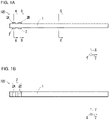
FIG. 1A is an external plan view of a piezoelectric element. -
FIG. 1B is an external side view of the piezoelectric element. -
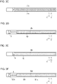
FIG. 2A is a cross-sectional view taken along line A-A inFIG. 1A . -
FIG. 2B is a cross-sectional view taken along line B-B inFIG. 1A . -
FIG. 2C is a cross-sectional view taken along line C-C inFIG. 1A . -
FIG. 3A is a diagram of an internal electrode pattern. -
FIG. 3B is a diagram of an internal electrode pattern. -
FIG. 3C is a diagram of an internal electrode pattern. -
FIG. 3D is a diagram of an internal electrode pattern. -
FIG. 3E is a diagram of an internal electrode pattern. -
FIG. 3F is a diagram of an internal electrode pattern. -
FIG. 4 is a diagram of a second conductor having another shape. - A piezoelectric element with the structure that forms the basis of a piezoelectric element according to one or more embodiments of the present disclosure includes piezoelectric layers and internal electrodes that are stacked on one another. The piezoelectric element is used as a piezoelectric actuator that deforms by bending with a voltage applied to the internal electrodes. Such a piezoelectric actuator can deform slightly with high precision.
- A piezoelectric actuator described in Patent Literature 1 is elongated along the Z-axis and has a distal end movable in the XY plane.
- To allow the distal end to move in the XY plane, the piezoelectric actuator includes internal electrodes in multiple patterns exposed on the side surfaces of the stack for connection to surface electrodes. The internal electrodes include extensions with their ends exposed at predetermined positions on the side surfaces. The internal electrodes illustrated in FIG. 16 of Patent Literature 1 have a small electrode width to prevent the piezoelectric layers from expanding or contracting due to their extensions. In this case, the stack can have non-uniform thicknesses between areas including the extensions of the internal electrodes and areas without including the extensions of the internal electrodes, thus lowering precision in deformation of the piezoelectric actuator by bending.
-
FIG. 1A is an external plan view of a piezoelectric element, andFIG, 1B is an external side view of the piezoelectric element.FIG. 2A is a cross-sectional view taken along line A-A inFIG. 1A .FIG. 2B is a cross-sectional view taken along line B-B inFIG. 1A .FIG. 2C is a cross-sectional view taken along line C-C inFIG. 1A . Apiezoelectric element 100 includes a stack 1 including internal electrodes 3 and piezoelectric layers 4 that are stacked on one another andsurface electrodes 2 located on side surfaces of the stack 1 and electrically connected to the internal electrodes 3. Thepiezoelectric element 100 according to the present embodiment is a piezoelectric actuator that applies a voltage to the internal electrodes 3 through thesurface electrodes 2 to cause the stacked piezoelectric layers 4 to deform by bending. As illustrated inFIGs. 1A and 1B , thepiezoelectric element 100 according to the present embodiment is, for example, a rectangular or quadrangular prism, and has one distal end in its longitudinal or axial direction movable as thepiezoelectric element 100 deforms by bending. Thesurface electrodes 2 are located on the two side surfaces of the other end opposite to the movable distal end. Thesurface electrodes 2 includesurface electrodes 2A on the two side surfaces of the other end, andsurface electrodes 2B on two side surfaces nearer the middle than thesurface electrodes 2A. The longitudinal or the axial direction is hereafter referred to as the Z-direction. The direction orthogonal to the Z-direction and connecting the two side surfaces on which thesurface electrodes 2 are located is referred to as the X-direction. The stacking direction orthogonal to the Z- and X-directions and in which the internal electrodes 3 and the piezoelectric layers 4 are stacked is referred to as the Y-direction. - As illustrated in the cross section of
FIG. 2A or other figures, the stack 1 includes multiple piezoelectric layers 4 and the internal electrodes 3 between the stacked piezoelectric layers 4. The internal electrodes 3 are exposed on the side surfaces of the other end of the stack 1 and are electrically connected to thesurface electrodes 2. The piezoelectric layers 4 include ceramics having piezoelectric properties. Examples of such ceramics include perovskite-type oxides containing lead zirconate titanate (PbZrO3-PbTiO3), lithium niobate (LiNbO3), and lithium tantalate (LiTaO3). The internal electrodes 3 may include, for example, a conductor containing, as a main component, silver or a silver-palladium alloy less reactive with ceramics or a conductor containing copper or platinum. Thesurface electrodes 2 may include, for example, the same or similar materials as the internal electrode 3, and may further be plated to prevent oxidation. - As described in detail later, the internal electrodes 3 include first electrodes 31 that apply a voltage to the piezoelectric layers 4 to cause the stack 1 to bend in a first direction (X-direction) orthogonal to the longitudinal direction (Z-direction) of the stack 1 and second electrodes 32 that apply a voltage to the piezoelectric layers 4 to cause the stack 1 to bend in a second direction (Y-direction) orthogonal to the longitudinal direction and the first direction. For example, the stack 1 is divided into substantially three areas in the stacking direction (Y-direction). The three areas include a
middle area 1M that causes thepiezoelectric element 100 to deform by bending in the X-direction (lateral direction). Themiddle area 1M includes the first electrodes 31. The three areas further include an upper area 1U and alower area 1L that cause thepiezoelectric element 100 to deform by bending in the Y-direction (vertical direction). The upper area 1U and thelower area 1L include the second electrodes 32. - For example, to cause the
piezoelectric element 100 to deform by bending in the X-direction, in themiddle area 1M, the first electrodes 31 receiving a voltage have an expanded right portion and a contracted left portion. This causes thepiezoelectric element 100 to bend to the left. The first electrodes 31 receiving a voltage can have a contracted right portion and an expanded left portion. This causes thepiezoelectric element 100 to bend to the right. Similarly, for example, to cause thepiezoelectric element 100 to deform by bending in the Y-direction, the second electrodes 32 receiving a voltage can have an expanded upper area 1U and a contractedlower area 1L. This causes thepiezoelectric element 100 to bend downward. The second electrodes 32 receiving a voltage can have a contracted upper area 1U and an expandedlower area 1L. This causes thepiezoelectric element 100 to bend upward. -
FIGs. 3A to 3F illustrate example patterns on the internal electrodes 3 in the present embodiment. These are example patterns on the second electrodes 32 in the upper area 1U, the first electrodes 31 in themiddle area 1M, and the second electrodes 32 in thelower area 1L. The patterns illustrated inFIGs. 3A and 3B are defined on the second electrodes 32 in the upper area 1U. The patterns illustrated inFIGs. 3C and 3D are defined on the first electrodes 31 in themiddle area 1M. The patterns illustrated inFIGs. 3E and 3F are defined on the second electrodes 32 in thelower area 1L. As described above, each of the areas includes the internal electrodes 3 having two different patterns. The internal electrodes 3 are alternately located between the piezoelectric layers 4 in the Y-direction. During the operation of thepiezoelectric element 100, a voltage is applied externally through thesurface electrodes 2 to generate a potential difference between the two different internal electrodes 3. Thepiezoelectric element 100 can deform by bending in the X- and Y-directions as described above. A voltage applied to thesurface electrodes 2 can be changed to control the degree by which and the direction in which the deformation by bending occurs. - The second electrodes 32 in the upper area 1U correspond to
second electrodes 32a each illustrated inFIG. 3A and tosecond electrodes 32b each illustrated inFIG. 3B . The second electrodes 32 in thelower area 1L correspond tosecond electrodes 32c each illustrated inFIG. 3E and tosecond electrodes 32d each illustrated inFIG. 3F . Eachsecond electrode 32b illustrated inFIG. 3B includes afirst conductor 321 including astrip 321a extending in the longitudinal direction and anextension 321b having one end continuous with thestrip 321a and the other end exposed on the side surface of the stack 1 and connected to thesurface electrode 2A. Thesecond electrode 32d illustrated inFIG. 3F has the same pattern as thesecond electrode 32b illustrated inFIG. 3B . Thesecond electrode 32d includes thefirst conductor 321, similarly to thesecond electrode 32b. Theextension 321b is, for example, substantially L-shaped. Theextension 321b has one end continuous with the middle of thestrip 321a and extending linearly in the Z-direction, and the other end bending at right angles toward the side surface of the stack 1 to be exposed on the side surface of the stack 1. Theextension 321b in substantially an L shape includes a wire 321b1 having a smaller width than thestrip 321a and a rectangular portion 321b2 continuous with the wire 321bl. The stack 1 includes, on the side surface on which theextensions 321b are exposed on the other end, theextensions 321b stacked on one another in the Y-direction. In the present embodiment, thepiezoelectric element 100 includessecond conductors 5 between theextensions 321b and a portion of the side surface of the stack 1 opposite to a portion of the side surface on which the other end of eachextension 321b is exposed. Thesecond conductors 5 in the present embodiment are rectangular and have the same length in the Z-direction as the rectangular portion 321b2 of theextension 321b. - The structure that forms the basis of the piezoelectric element according to one or more embodiments of the present disclosure includes no
second conductors 5 between the side surfaces of the stack 1 and theextensions 321b, and includes a portion with theextensions 321b thicker than an opposite portion in the X-direction, thus causing thepiezoelectric element 100 to have non-uniform thickness and have lower precision in the deformation by bending. In the present embodiment, thesecond conductor 5 reduces the non-uniform thickness of the stack 1 and thus reduces the likelihood that thepiezoelectric element 100 deforms by bending with lower precision. - The
piezoelectric element 100 may have any dimensions of, but not limited to, a length of 1 to 3 mm in the X-direction, a length of 1 to 2 mm in the Y-direction, and a length of 20 to 50 mm in the Z-direction. The internal electrodes 3 may each have a thickness of 0.1 to 5 µm. The piezoelectric layers 4 may each have a thickness of 0.01 to 0.1 mm. Thesecond conductors 5 may each have, for example, a width of 1 to 2.5 mm (dimension in the X-direction) and a length of 1 to 3 mm (dimension in the Z-direction). - The first electrodes 31 in the
middle area 1M correspond tofirst electrodes 31a each illustrated inFIG. 3C and tofirst electrodes 31b each illustrated inFIG. 3D . Eachfirst electrode 31b has a pattern symmetrical to the pattern on thesecond electrode 32b with respect to the Z-direction. More specifically, in the present embodiment, thefirst electrode 31b inFIG. 3D includes a first conductor 321'. The first conductor 321' is symmetrical to thefirst conductor 321 of thesecond electrode 32b inFIG. 3B with respect to the Z-direction. Themiddle area 1M includes thesecond conductors 5, similarly to the upper area 1U. In the present embodiment, thesecond electrode 32d inFIG. 3F includes the samefirst conductor 321 as thesecond electrode 32b inFIG. 3B . Thelower area 1L also includes thesecond conductors 5, similarly to the upper area 1U. - Additionally, the
second electrode 32a illustrated inFIG. 3A and thesecond electrode 32c illustrated inFIG. 3E include afirst conductor 321 and a first conductor 321' having a similar shape to thefirst conductor 321 and the first conductor 321'. The upper area 1U and thelower area 1L further include thesecond conductors 5. - Although the
second conductors 5 are included in all the upper area 1U, themiddle area 1M, and thelower area 1L in the present embodiment as described above, thesecond conductors 5 may not be included in all the areas. One or moresecond conductors 5 included in the areas can reduce the non-uniform thickness of the stack 1 compared with a piezoelectric element with the structure that forms the basis of the piezoelectric element according to one or more embodiments of the present disclosure with nosecond conductors 5. - In the present embodiment, the
second conductors 5 are exposed on the side surfaces of the stack 1 and connected to thesurface electrodes surface electrodes 2 on the side surfaces of the stack 1 to enhance mechanical strength. As described above, thesecond conductors 5 effectively reduce the non-uniform thickness of the stack 1. Thesecond conductors 5 may not be electrically connected to thesurface electrodes 2. For example, thesecond conductors 5 may not be exposed on the side surfaces of the stack 1 and may entirely be buried between the piezoelectric layers 4. - This structure can reduce the non-uniform thickness of the stack 1 although the
first conductor 321 and thesecond conductor 5 have different characteristics. Thus, for example, thefirst conductor 321 and thesecond conductor 5 may include the same or different materials. When thefirst conductor 321 and thesecond conductor 5 include the same material, the two conductors can have a smaller thickness difference between them, thus further reducing the non-uniform thickness of the stack 1. - Another embodiment will now be described. The structure according to the present embodiment is the same as in the above embodiment except that the shape of the second conductor, and thus a second conductor having another shape and a first conductor are illustrated in
FIG. 4 . The other structure will not be illustrated or described. Asecond conductor 5A in the present embodiment is rectangular and has round corners adjacent to anextension 321b of thefirst conductor 321. Thesecond conductor 5 having sharp corners instead of the round corners as described in the above embodiment is likely to cause a short circuit due to electric discharge between thesecond conductor 5 and theextension 321b. To prevent this, a gap is left between thesecond conductor 5 and theextension 321b of thefirst conductor 321. The gap reduces an area for thesecond conductor 5. Thesecond conductor 5A having round corners allows the distance between thesecond conductor 5A and theextension 321b to be shorter. This enlarges thesecond conductor 5A and reduces the gap to reduce the non-uniform thickness of the stack 1 further. - The operation of the
piezoelectric element 100 will be described briefly. First, the electrical connection between thesurface electrodes 2 and the internal electrodes 3 will be described. Onesurface electrode 2A is electrically connected to thesecond electrodes 32b in the upper area 1U and thesecond electrodes 32d in thelower area 1L. Theother surface electrode 2A is electrically connected to thefirst electrodes 31b in themiddle area 1M. Onesurface electrode 2B is electrically connected to thesecond electrodes 32a in the upper area 1U and thefirst electrodes 31a (at one side) in themiddle area 1M. Theother surface electrode 2B is electrically connected to thefirst electrodes 31a (at the other side) in themiddle area 1M and thesecond electrodes 32c in thelower area 1L. The polarization direction of the piezoelectric layers 4 includes a first direction and a second direction. One side of each of the upper area 1U and themiddle area 1M is the first direction. The other side of each of thelower area 1L and themiddle area 1M opposite to the first direction is the second direction. For example, thesurface electrodes 2A are set to a ground potential. A voltage of -64 V is applied to onesurface electrode 2B and +64 V to theother surface electrode 2B to polarize the piezoelectric layers 4 as described above. - A constant voltage is applied to each of the
surface electrodes 2B during operation. An example voltage to be applied is +11 V to onesurface electrode 2B and +61 V to theother surface electrode 2B. A voltage of 0 to +72 V applied to both thesurface electrodes 2A can cause thepiezoelectric element 100 to deform by bending in an intended direction. For example, a voltage of +72 V is applied to onesurface electrode 2A and +36 V to theother surface electrode 2A to cause thepiezoelectric element 100 to deform by bending (maximum) in one Y-direction (upward), and a voltage of 0 V is applied to onesurface electrode 2A and +36 V to theother surface electrode 2A to cause thepiezoelectric element 100 to deform by bending (maximum) in the other Y-direction (downward). In other words, a voltage of 0 to +72 V is applied to onesurface electrode 2A, and a constant voltage of +36 V is applied to theother surface electrode 2A to adjust the degree by which the deformation by bending occurs in the Y-direction. For example, a voltage of +36 V is applied to onesurface electrode 2A and +72 V to theother surface electrode 2A to cause thepiezoelectric element 100 to deform by bending (maximum) in one X-direction (rightward). A voltage of +36 V is applied to onesurface electrode 2A and 0 V to theother surface electrode 2A to cause thepiezoelectric element 100 to deform by bending (maximum) in the other X-direction (leftward). In other words, a constant voltage of +36 V is applied to onesurface electrode 2A, and a voltage of 0 to +72 V is applied to theother surface electrode 2A to adjust the degree by which the deformation by bending occurs in the X-direction. A voltage to be applied to both thesurface electrodes 2A is changed within the range of 0 to +72 V to cause the deformation by bending in an oblique direction. - The present disclosure may be implemented in the following forms.
- A piezoelectric element according to one or more embodiments of the present disclosure includes a stack including a plurality of internal electrodes and a plurality of piezoelectric layers stacked on one another, and a surface electrode located on a side surface of the stack and connected to the plurality of internal electrodes. The plurality of internal electrodes include a first electrode configured to apply a voltage to the plurality of piezoelectric layers to cause the stack to bend in a first direction orthogonal to a longitudinal direction of the stack, and a second electrode configured to apply a voltage to the plurality of piezoelectric layers to cause the stack to bend in a second direction orthogonal to the longitudinal direction and the first direction. At least one of the first electrode or the second electrode includes a first conductor including a strip extending in the longitudinal direction and an extension having one end continuous with the strip and another end exposed on the side surface of the stack and connected to the surface electrode. The piezoelectric element includes a second conductor located between the extension and an opposite portion of the side surface opposite to a portion of the side surface on which the other end of the extension is exposed.
- The piezoelectric element according to the embodiments of the present disclosure includes the second conductors to reduce the non-uniform thickness of the stack, and to reduce the likelihood of the deformation by bending with lower precision.
- Although embodiments of the present disclosure have been described in detail, the present disclosure is not limited to the embodiments described above, and may be changed or modified in various manners without departing from the spirit and scope of the present disclosure. The components described in the above embodiments may be entirely or partially combined as appropriate unless any contradiction arises.
-
- 1 stack
- 1L lower area
- 1M middle area
- 1U upper area
- 2, 2A, 2B surface electrode
- 3 internal electrode
- 4 piezoelectric layer
- 5, 5A second conductor
- 31, 31a, 31b first electrode
- 32, 32a, 32b, 32c, 32d second electrode
- 100 piezoelectric element
- 321, 321' first conductor
- 321a strip
- 321b extension
- 321b1 wire
- 321b2 rectangular portion
Claims (6)
- A piezoelectric element, comprising:
a stack including a plurality of internal electrodes and a plurality of piezoelectric layers; anda surface electrode located on a side surface of the stack and electrically connected to the plurality of internal electrode,wherein the plurality of internal electrodes includesa first electrode configured to bend the stack in a first direction perpendicular to a longitudinal direction of the stack body by applying a voltage to the piezoelectric layers, anda second electrode configured to bend the stack in a second direction perpendicular to the longitudinal direction and the first direction by applying a voltage to the piezoelectric layers,at least one of the first electrode or the second electrode comprising:
a first conductor comprising:a strip extending in the longitudinal direction; andan extension one end of which is connected to the strip, and another end of which is exposed at the side surface of the stack and connected to the surface electrode; anda second conductor between the extension and a portion opposite to an other portion where the another end of the extension is exposed. - The piezoelectric element according to claim 1, wherein the first conductor and the second conductor is composed of a same material.
- The piezoelectric element according to claim 1 or claim 2, the second conductor is exposed to the portion opposite to the other portion of the side surface.
- The piezoelectric element according to any one of claims 1 to 3, wherein the second conductor has a rectangular shape, and includes a round corner adjacent to the extension.
- The piezoelectric element according to any one of claims 1 to 3, whereineach of the first electrode and the second electrode each includes the first conductor, andin a plan view, a portion of the side surface on which the extension of the first conductor included in the first electrode is exposed is located opposite to a portion of the side surface on which the extension of the first conductor included in the second electrode is exposed.
- The piezoelectric element according to any one of claims 1 to 5, wherein the extension includesa wire including the one end and having smaller width than the strip, anda rectangular portion including the other end and connected to the wire.
Applications Claiming Priority (2)
| Application Number | Priority Date | Filing Date | Title |
|---|---|---|---|
| JP2020019622 | 2020-02-07 | ||
| PCT/JP2021/003533 WO2021157522A1 (en) | 2020-02-07 | 2021-02-01 | Piezoelectric element |
Publications (2)
| Publication Number | Publication Date |
|---|---|
| EP4102582A1 true EP4102582A1 (en) | 2022-12-14 |
| EP4102582A4 EP4102582A4 (en) | 2024-03-13 |
Family
ID=77200187
Family Applications (1)
| Application Number | Title | Priority Date | Filing Date |
|---|---|---|---|
| EP21750278.0A Pending EP4102582A4 (en) | 2020-02-07 | 2021-02-01 | PIEZOELECTRIC ELEMENT |
Country Status (5)
| Country | Link |
|---|---|
| US (1) | US12615966B2 (en) |
| EP (1) | EP4102582A4 (en) |
| JP (1) | JP7467511B2 (en) |
| CN (1) | CN115039243B (en) |
| WO (1) | WO2021157522A1 (en) |
Family Cites Families (11)
| Publication number | Priority date | Publication date | Assignee | Title |
|---|---|---|---|---|
| DE19605214A1 (en) * | 1995-02-23 | 1996-08-29 | Bosch Gmbh Robert | Ultrasonic drive element |
| GB2378573B (en) * | 2001-06-20 | 2003-09-10 | Polatis Ltd | A piezoelectric actuator |
| JP4249472B2 (en) | 2002-11-20 | 2009-04-02 | 大日本印刷株式会社 | Rolled packaging material storage carton |
| JP4720068B2 (en) * | 2003-03-03 | 2011-07-13 | Tdk株式会社 | Multilayer piezoelectric element |
| JP2005191047A (en) * | 2003-12-24 | 2005-07-14 | Kyocera Corp | Multilayer piezoelectric element and injection device |
| WO2009028348A1 (en) * | 2007-08-27 | 2009-03-05 | Ngk Insulators, Ltd. | Method for polarizing laminated piezoelectric/electrostrictive element |
| WO2010035437A1 (en) | 2008-09-26 | 2010-04-01 | 株式会社村田製作所 | Piezoelectric stack |
| WO2015114849A1 (en) | 2014-01-30 | 2015-08-06 | 京セラ株式会社 | Piezoelectric element and piezoelectric vibrating apparatus, handheld terminal, sound generator, sound-generating apparatus, and electronic device containing said piezoelectric element |
| JP6932935B2 (en) | 2017-02-01 | 2021-09-08 | Tdk株式会社 | Piezoelectric actuator |
| JP7163570B2 (en) * | 2017-09-20 | 2022-11-01 | Tdk株式会社 | Laminated piezoelectric element and vibration device |
| EP4177976B1 (en) * | 2020-07-03 | 2025-09-10 | Kyocera Corporation | Piezoelectric element |
-
2021
- 2021-02-01 WO PCT/JP2021/003533 patent/WO2021157522A1/en not_active Ceased
- 2021-02-01 EP EP21750278.0A patent/EP4102582A4/en active Pending
- 2021-02-01 US US17/796,923 patent/US12615966B2/en active Active
- 2021-02-01 JP JP2021575781A patent/JP7467511B2/en active Active
- 2021-02-01 CN CN202180012346.1A patent/CN115039243B/en active Active
Also Published As
| Publication number | Publication date |
|---|---|
| US12615966B2 (en) | 2026-04-28 |
| WO2021157522A1 (en) | 2021-08-12 |
| EP4102582A4 (en) | 2024-03-13 |
| CN115039243B (en) | 2025-12-26 |
| JP7467511B2 (en) | 2024-04-15 |
| US20230058604A1 (en) | 2023-02-23 |
| CN115039243A (en) | 2022-09-09 |
| JPWO2021157522A1 (en) | 2021-08-12 |
Similar Documents
| Publication | Publication Date | Title |
|---|---|---|
| KR100259674B1 (en) | Laminated piezoelectric transformer and method of manufacturing the same | |
| JPH06224484A (en) | Piezoelectric porcelain transformer and driving method therefor | |
| CN109119529B (en) | Laminated piezoelectric element, piezoelectric vibration device, and electronic apparatus | |
| US5892318A (en) | Piezoelectric transformer with multiple output | |
| US5266862A (en) | Piezoelectric actuator | |
| CN101373811A (en) | Piezoelectric driven MEMS device and portable terminal | |
| US20250087393A1 (en) | Stacked varistor | |
| EP4177976B1 (en) | Piezoelectric element | |
| KR101421424B1 (en) | Multilayer capacitor | |
| EP1814170A2 (en) | Piezoelectric/electrostrictive actuator | |
| JP7071172B2 (en) | Laminated piezoelectric elements, piezoelectric vibration devices, and electronic devices | |
| US12615966B2 (en) | Two axis piezoelectric element | |
| US20230329118A1 (en) | Piezoelectric driving element | |
| US11944999B2 (en) | Vibration device and piezoelectric element | |
| JP7528239B2 (en) | Piezoelectric Actuator | |
| JP6809822B2 (en) | Piezoelectric actuator | |
| JP3106603B2 (en) | Piezo actuator | |
| US20250386733A1 (en) | Piezoelectric element | |
| JP7596398B2 (en) | Piezoelectric Actuator | |
| KR102626610B1 (en) | Stacked Piezoelectric device and piezoelectric actuator including the same | |
| JP3567330B2 (en) | Multilayer type piezoelectric ceramic actuator | |
| JPH0476968A (en) | Manufacture of laminated piezoelectric element | |
| JPH0590657A (en) | Laminated piezoelectric actuator and method for manufacturing the same | |
| JPS59175531A (en) | Piezoelectric relay | |
| JP2011071359A (en) | Wiring board |
Legal Events
| Date | Code | Title | Description |
|---|---|---|---|
| STAA | Information on the status of an ep patent application or granted ep patent |
Free format text: STATUS: THE INTERNATIONAL PUBLICATION HAS BEEN MADE |
|
| PUAI | Public reference made under article 153(3) epc to a published international application that has entered the european phase |
Free format text: ORIGINAL CODE: 0009012 |
|
| STAA | Information on the status of an ep patent application or granted ep patent |
Free format text: STATUS: REQUEST FOR EXAMINATION WAS MADE |
|
| 17P | Request for examination filed |
Effective date: 20220801 |
|
| AK | Designated contracting states |
Kind code of ref document: A1 Designated state(s): AL AT BE BG CH CY CZ DE DK EE ES FI FR GB GR HR HU IE IS IT LI LT LU LV MC MK MT NL NO PL PT RO RS SE SI SK SM TR |
|
| DAV | Request for validation of the european patent (deleted) | ||
| DAX | Request for extension of the european patent (deleted) | ||
| P01 | Opt-out of the competence of the unified patent court (upc) registered |
Effective date: 20230505 |
|
| REG | Reference to a national code |
Ref country code: DE Ref legal event code: R079 Free format text: PREVIOUS MAIN CLASS: H01L0041047000 Ipc: H10N0030200000 |
|
| A4 | Supplementary search report drawn up and despatched |
Effective date: 20240213 |
|
| RIC1 | Information provided on ipc code assigned before grant |
Ipc: H10N 30/87 20230101ALI20240208BHEP Ipc: H10N 30/50 20230101ALI20240208BHEP Ipc: H10N 30/20 20230101AFI20240208BHEP |
|
| STAA | Information on the status of an ep patent application or granted ep patent |
Free format text: STATUS: EXAMINATION IS IN PROGRESS |
|
| 17Q | First examination report despatched |
Effective date: 20241212 |
|
| GRAP | Despatch of communication of intention to grant a patent |
Free format text: ORIGINAL CODE: EPIDOSNIGR1 |
|
| STAA | Information on the status of an ep patent application or granted ep patent |
Free format text: STATUS: GRANT OF PATENT IS INTENDED |
|
| INTG | Intention to grant announced |
Effective date: 20260211 |