EP4102564A1 - Interference filter and electrostatic discharge / electrical surge protection circuit and device - Google Patents
Interference filter and electrostatic discharge / electrical surge protection circuit and device Download PDFInfo
- Publication number
- EP4102564A1 EP4102564A1 EP22177826.9A EP22177826A EP4102564A1 EP 4102564 A1 EP4102564 A1 EP 4102564A1 EP 22177826 A EP22177826 A EP 22177826A EP 4102564 A1 EP4102564 A1 EP 4102564A1
- Authority
- EP
- European Patent Office
- Prior art keywords
- terminal
- bipolar transistor
- resistor
- electrically coupled
- circuit
- Prior art date
- Legal status (The legal status is an assumption and is not a legal conclusion. Google has not performed a legal analysis and makes no representation as to the accuracy of the status listed.)
- Pending
Links
Images




Classifications
-
- H—ELECTRICITY
- H03—ELECTRONIC CIRCUITRY
- H03H—IMPEDANCE NETWORKS, e.g. RESONANT CIRCUITS; RESONATORS
- H03H11/00—Networks using active elements
- H03H11/02—Multiple-port networks
- H03H11/04—Frequency selective two-port networks
-
- H—ELECTRICITY
- H10—SEMICONDUCTOR DEVICES; ELECTRIC SOLID-STATE DEVICES NOT OTHERWISE PROVIDED FOR
- H10D—INORGANIC ELECTRIC SEMICONDUCTOR DEVICES
- H10D89/00—Aspects of integrated devices not covered by groups H10D84/00 - H10D88/00
- H10D89/60—Integrated devices comprising arrangements for electrical or thermal protection, e.g. protection circuits against electrostatic discharge [ESD]
- H10D89/601—Integrated devices comprising arrangements for electrical or thermal protection, e.g. protection circuits against electrostatic discharge [ESD] for devices having insulated gate electrodes, e.g. for IGFETs or IGBTs
- H10D89/711—Integrated devices comprising arrangements for electrical or thermal protection, e.g. protection circuits against electrostatic discharge [ESD] for devices having insulated gate electrodes, e.g. for IGFETs or IGBTs using bipolar transistors as protective elements
-
- H—ELECTRICITY
- H02—GENERATION; CONVERSION OR DISTRIBUTION OF ELECTRIC POWER
- H02H—EMERGENCY PROTECTIVE CIRCUIT ARRANGEMENTS
- H02H9/00—Emergency protective circuit arrangements for limiting excess current or voltage without disconnection
- H02H9/04—Emergency protective circuit arrangements for limiting excess current or voltage without disconnection responsive to excess voltage
- H02H9/045—Emergency protective circuit arrangements for limiting excess current or voltage without disconnection responsive to excess voltage adapted to a particular application and not provided for elsewhere
- H02H9/046—Emergency protective circuit arrangements for limiting excess current or voltage without disconnection responsive to excess voltage adapted to a particular application and not provided for elsewhere responsive to excess voltage appearing at terminals of integrated circuits
-
- H—ELECTRICITY
- H02—GENERATION; CONVERSION OR DISTRIBUTION OF ELECTRIC POWER
- H02H—EMERGENCY PROTECTIVE CIRCUIT ARRANGEMENTS
- H02H9/00—Emergency protective circuit arrangements for limiting excess current or voltage without disconnection
- H02H9/04—Emergency protective circuit arrangements for limiting excess current or voltage without disconnection responsive to excess voltage
- H02H9/045—Emergency protective circuit arrangements for limiting excess current or voltage without disconnection responsive to excess voltage adapted to a particular application and not provided for elsewhere
-
- H—ELECTRICITY
- H03—ELECTRONIC CIRCUITRY
- H03H—IMPEDANCE NETWORKS, e.g. RESONANT CIRCUITS; RESONATORS
- H03H7/00—Multiple-port networks comprising only passive electrical elements as network components
- H03H7/01—Frequency selective two-port networks
- H03H7/0138—Electrical filters or coupling circuits
-
- H—ELECTRICITY
- H03—ELECTRONIC CIRCUITRY
- H03H—IMPEDANCE NETWORKS, e.g. RESONANT CIRCUITS; RESONATORS
- H03H7/00—Multiple-port networks comprising only passive electrical elements as network components
- H03H7/01—Frequency selective two-port networks
- H03H7/17—Structural details of sub-circuits of frequency selective networks
- H03H7/1741—Comprising typical LC combinations, irrespective of presence and location of additional resistors
- H03H7/1766—Parallel LC in series path
-
- H—ELECTRICITY
- H10—SEMICONDUCTOR DEVICES; ELECTRIC SOLID-STATE DEVICES NOT OTHERWISE PROVIDED FOR
- H10D—INORGANIC ELECTRIC SEMICONDUCTOR DEVICES
- H10D89/00—Aspects of integrated devices not covered by groups H10D84/00 - H10D88/00
- H10D89/60—Integrated devices comprising arrangements for electrical or thermal protection, e.g. protection circuits against electrostatic discharge [ESD]
-
- H—ELECTRICITY
- H10—SEMICONDUCTOR DEVICES; ELECTRIC SOLID-STATE DEVICES NOT OTHERWISE PROVIDED FOR
- H10W—GENERIC PACKAGES, INTERCONNECTIONS, CONNECTORS OR OTHER CONSTRUCTIONAL DETAILS OF DEVICES COVERED BY CLASS H10
- H10W42/00—Arrangements for protection of devices
- H10W42/20—Arrangements for protection of devices protecting against electromagnetic or particle radiation, e.g. light, X-rays, gamma-rays or electrons
Definitions
- This disclosure relates to circuits, such as circuits that can be implemented in a semiconductor device. More specifically, this disclosure relates to circuits and devices for providing linear electromagnetic interference filtering, as well as protection from electrostatic discharge and/or electrical surge events.
- EMI filter devices implemented in mobile device technologies, such as fifth-generation (5G) wireless technologies, can be subjected to increasing EMI levels, e.g., due to increased radio frequency (RF) of operation and/or additional antennas being added, as compared to previous devices.
- RF radio frequency
- scaling to smaller technologies also presents challenges in meeting electrostatic discharge (ESD) and electrical (voltage and/or current) surge protection target specifications.
- ESD electrostatic discharge
- electrical voltage and/or current
- an electromagnetic interference (EMI) filter circuit including: an input terminal; an output terminal; an electrical ground terminal; a resistor electrically coupled between the input terminal and the output terminal; a first bipolar transistor including: a collector terminal electrically coupled with the input terminal; an emitter terminal electrically coupled with the electrical ground terminal; and a base terminal that is electrically floating; and a second bipolar transistor including: a collector terminal electrically coupled with the output terminal; an emitter terminal electrically coupled with the electrical ground terminal; and a base terminal that is electrically floating.
- EMI electromagnetic interference
- the techniques described herein relate to a EMI filter circuit, wherein the resistor is a first resistor, the EMI filter circuit further including: a second resistor electrically coupled in series with the first resistor between the input terminal and the output terminal; and a third bipolar transistor including: a collector terminal electrically coupled between the first resistor and the second resistor; an emitter terminal electrically coupled with the electrical ground terminal; and a base terminal that is electrically floating.
- the techniques described herein relate to a EMI filter circuit, wherein: the EMI filter circuit is included in a semiconductor device; the first bipolar transistor is a first vertical bipolar transistor; the second bipolar transistor is a second vertical bipolar transistor; and the third bipolar transistor is a third vertical bipolar transistor.
- the techniques described herein relate to a EMI filter circuit, further including: an inductive-capacitive (LC) circuit including: an inductor; and a capacitor electrically coupled in parallel with the inductor, the LC circuit being electrically coupled in series with the resistor between the input terminal and the output terminal.
- LC inductive-capacitive
- the techniques described herein relate to a EMI filter circuit, wherein the resistor is a first resistor and the LC circuit is a first LC circuit, the EMI filter circuit further including: a second resistor; and a second LC circuit, the first resistor, the first LC circuit, the second LC circuit, and the second resistor being electrically coupled in series between the input terminal and the output terminal, the EMI filter circuit further including: a third bipolar transistor including: a collector terminal electrically coupled between the first LC circuit and the second LC circuit; an emitter terminal electrically coupled with the electrical ground terminal; and a base terminal that is electrically floating.
- the techniques described herein relate to a EMI filter circuit, wherein the resistor is a first resistor, the EMI filter circuit further including: a second resistor electrically coupled in series with the first resistor between the input terminal and the output terminal.
- the techniques described herein relate to a EMI filter circuit, wherein: the EMI filter circuit is included in a semiconductor device; the first bipolar transistor is a first vertical bipolar transistor; the first resistor is a first diffusion resistor; the second bipolar transistor is a second vertical bipolar transistor; and the second resistor is a second diffusion resistor.
- the techniques described herein relate to a semiconductor device including: a substrate of a first conductivity type; a semiconductor layer of a second conductivity type that is opposite the first conductivity type; a first isolation region defined by a first trench; a first diffusion region of the first conductivity type disposed in the semiconductor layer in the first isolation region; a second isolation region defined by a second trench; a second diffusion region of the first conductivity type disposed in the semiconductor layer in the second isolation region; an electrical ground terminal disposed on the semiconductor layer outside the first isolation region and outside the second isolation region; and an electromagnetic interference (EMI) filter circuit including: an input terminal disposed on the semiconductor layer in the first isolation region; an output terminal disposed on the semiconductor layer in the second isolation region; a first electrical impedance element disposed in the first isolation region; a second electrical impedance element disposed in the second isolation region, the first electrical impedance element and the second electrical impedance element being electrically coupled in series between the input terminal and the output terminal; a first vertical bipolar transistor disposed in the first
- the techniques described herein relate to a semiconductor device, wherein: the first trench extends from an upper surface of the semiconductor layer, through the semiconductor layer and terminates in the substrate, the first trench having a dielectric material disposed therein; and the second trench extends from the upper surface of the semiconductor layer, through the semiconductor layer and terminates in the substrate, the second trench having the dielectric material disposed therein.
- the techniques described herein relate to a semiconductor device, wherein the electrical ground terminal is electrically coupled with the substrate via a plurality of trenches filled with an electrically conductive material.
- the techniques described herein relate to a semiconductor device, wherein the plurality of trenches extend from a surface of the semiconductor layer, through the semiconductor layer and terminate in the substrate.
- the techniques described herein relate to a semiconductor device, wherein: the first electrical impedance element is a first diffusion resistor included in the first diffusion region; and the second electrical impedance element is a second diffusion resistor included in the second diffusion region.
- the techniques described herein relate to a semiconductor device, wherein: the collector terminal of the first vertical bipolar transistor is included in the first diffusion region; the base terminal of the first vertical bipolar transistor is included in the semiconductor layer; the emitter terminal of the first vertical bipolar transistor is included in the substrate; the collector terminal of the second vertical bipolar transistor is included in the second diffusion region; the base terminal of the second vertical bipolar transistor is included in the semiconductor layer; and the emitter terminal of the second vertical bipolar transistor is included in the substrate.
- the techniques described herein relate to a semiconductor device, wherein: the first electrical impedance element is a resistor; and the second electrical impedance element is an inductive-capacitive (LC) circuit.
- the first electrical impedance element is a resistor
- the second electrical impedance element is an inductive-capacitive (LC) circuit.
- the techniques described herein relate to a semiconductor device, wherein the first diffusion region includes: a first region disposed in the semiconductor layer, the first region having a first doping concentration; and a second region disposed in the first region, the second region having a second doping concentration that is greater than the first doping concentration.
- the techniques described herein relate to a semiconductor device, wherein: the first conductivity type is n-type; and the second conductivity type is p-type.
- the techniques described herein relate to a method including: receiving an electrical transient at one of an input terminal, an output terminal, or an electrical ground terminal of an electromagnetic interference (EMI) filter circuit; clamping a voltage of the electrical transient with a vertical, open-base bipolar transistor of the EMI filter circuit; conducting a first portion of a current of the electrical transient with the vertical, open-base bipolar transistor; and conducting a second portion of the current of the electrical transient with an electrical impedance element of the EMI filter circuit, the second portion of the current being less than the first portion of the current, a collector terminal of the vertical, open-base bipolar transistor being electrically coupled with one of the input terminal or the output terminal, an emitter terminal of the vertical, open-base bipolar transistor being electrically coupled with the electrical ground terminal, and the electrical impedance element being electrically coupled between the input terminal and the output terminal.
- EMI electromagnetic interference
- the techniques described herein relate to a method, wherein the electrical transient is one of an electrostatic discharge (ESD) or an electrical surge.
- ESD electrostatic discharge
- the techniques described herein relate to a method, wherein the electrical impedance element includes at least one of a diffusion resistor or an inductive-capacitive circuit.
- the techniques described herein relate to a method, wherein the vertical, open-base bipolar transistor and the electrical impedance element are included in an isolation region of the EMI filter circuit.
- EMI electromagnetic interference
- ESD electrostatic discharge
- electrical surge protection devices and their operation
- the illustrated devices include a number of similar aspects, as well as a number of variations from one illustrated implementation to another.
- an EMI filter of such a device can include active, open-base bipolar transistors and electrical impedance elements (e.g., resistors, capacitors, and/or inductors) that provide for linear filtering of EMI that can occur as a result of radio frequency noise, as well as associated harmonics, that can be wirelessly coupled onto an associated data path and/or can occur due to non-linearity of the EMI filter, where the data path is configured to communicate digital information (data) associated with operation of a corresponding wireless communication device (e.g., a mobile phone, etc.), e.g., at frequencies that are more than an order of magnitude lower than radio frequencies.
- a corresponding wireless communication device e.g., a mobile phone, etc.
- collector-to-base capacitances, base-to emitter capacitances and/or distributed capacitances of the electrical impedance elements can be adjusted to achieved desired EMI filtering (e.g., linearity and attenuation) performance.
- the open-base bipolar transistors and electrical impedance elements can be included in (disposed in, etc.) respective isolation regions in a semiconductor device.
- the isolated open-base bipolar transistors and electrical impedance elements can, in addition to providing for EMI filtering, prevent damage to the EMI filter device from ESD and/or electrical surge (e.g., over-current and/or overvoltage) events.
- EMI filtering performance of example implementations can be tuned by adjusting junction capacitances of the open-base bipolar transistors and/or distributed capacitances of the electrical impedance elements, e.g., by adjusting doping concentrations, and/or adjusting layout and sizing of the circuit elements of the EMI filter, and so forth.
- EMI filter performance can also be adjusted (tuned) by adjusting impedances of impedance elements included in the EMI filter (e.g., using similar techniques as those for adjusting capacitances).
- one or more aspects of one implementation can be likewise implemented in one or more other implementations.
- arrangement and relative sizes of implants, specific circuit elements, etc., shown in one example implementation could also be implemented in other implementations.
- circuit elements e.g., transistors, resistors, capacitors, inductors
- circuit elements can be added to, substituted for, or removed.
- example devices and circuits are described herein as being implemented with specific conductivity types (e.g., n-type or p-type) for specific implants and/or regions (e.g., diffusion regions).
- the doping concentrations of each of these implants and/or regions can vary based on the particular implementation.
- qualitative examples of doping concentration e.g., lightly doped, heavily doped, very-heavily doped, and so forth
- these qualitative indications of doping concentration are relative. That is, as used herein, lightly doped indicates lower doping concentration than heavily doped, while heavily doped indicates lower doping concentration than very-heavily doped.
- the conductivity types of the various regions described herein can be inverted. That is, regions of the example devices described as being n-type can be implemented as p-type, and regions described as being p-type can be implemented as n-type, NPN transistors can be implemented as PNP transistors, etc.
- FIG. 1A is a block diagram schematically illustrating an example EMI filter and ESD / electrical surge protection device (e.g., device 100).
- the device 100 includes an isolation region 110, an isolation region 120, an electrical ground region 130, an electrical ground region 140, and an electrical interconnection 150.
- portions of the device 100 can be replicated and/or mirrored to create devices that implement higher order filters, such as the examples shown in FIGs. 3A to 3C .
- the isolation region 110 is defined by an isolation trench 112, which can be a dielectric filled trench.
- the isolation region 120 is defined by an isolation trench 122, which can also be a dielectric filled trench.
- the device 100 can include circuit elements that are respectively implemented in the isolation region 110 and the isolation region 120. In implementations, these circuit elements can be configured to implement an EMI filter circuit, as well as to provide ESD and electrical surge protection for the device 100. For instance, as shown in FIG.
- a transistor 114 e.g., a vertical, bipolar transistor
- an electrical impedance element 118 can be implemented in the isolation region 110
- a transistor 124 e.g., a vertical, bipolar transistor
- an electrical impedance element 128 can be implemented in the isolation region 120.
- a signal pad e.g., an input terminal 116) of the corresponding EMI filter circuit can also be included in the isolation region 110
- a signal pad e.g., an output terminal 126) of the corresponding EMI filter circuit can be included in the isolation region 120.
- the electrical impedance element 118 and the electrical impedance element 128 can respectively include resistors, inductors and/or capacitors, such as in the examples described herein. The specific circuit elements of the device 100 will depend on the particular implementation.
- the ground region 130 and the ground region 140 can each include a plurality of conductive trenches, e.g., arrays of trenches filled with an electrically conductive material, such as tungsten.
- the conductive trenches can electrically couple, respectively, an electrical ground terminal 132 (e.g., signal pad) of the electrical ground region 130 and an electrical ground terminal 142 (e.g., signal pad) of the electrical ground region 140 with a semiconductor substrate of the device 100.
- such conductive trenches can provide low resistance, and low inductance electrical connections from the electrical ground terminal 132 and the electrical ground terminal 142 to an associated semiconductor substrate, so as to reduce adverse impacts on linearity and attenuation performance of the corresponding EMI filter circuit due to electrical impedance (e.g., resistance and inductance) of the electrical ground connections.
- electrical interconnection 150 in this example, electrically couples the electrical impedance element 118 with the electrical impedance element 128.
- FIG. 1A also includes a section line C-C, which corresponds with the cross-sectional view shown in FIG. 2 .
- the section line C-C extends through the isolation region 110, through the electrical ground region 130, and through the isolation region 120. That is, the section line C-C is not a straight line, such that the isolation region 110, the electrical ground region 130 and the isolation region 120 of the device 100 (and their corresponding regions in FIG. 2 ) are included the cross-section defined by the section line C-C.
- FIG. 1 B is a schematic diagram illustrating an EMI filter and electrostatic ESD / electrical surge protection circuit (circuit 100a) that can be implemented in the device 100 of FIG. 1A .
- circuit 100a an EMI filter and electrostatic ESD / electrical surge protection circuit
- elements of the circuit 100a corresponding with elements of the device 100 are referenced with like 100 series reference numbers suffixed with the letter 'a.'
- elements of the circuit 100a can be replaced with other elements, additional elements can be added, and/or elements can be removed.
- the circuit 100a includes an open-base bipolar transistor 114a, and an open-base bipolar transistor 124a.
- respective base terminals of the open-base bipolar transistor 114a and the open-base bipolar transistor 124a can be electrically floating.
- an input terminal 116a can be electrically coupled with a collector terminal of the open-base bipolar transistor 114a, while an output terminal 126a can be electrically coupled with a collector terminal of the open-base bipolar transistor 124a.
- a resistor 118a and a resistor 128a can be electrically coupled in series between the input terminal 116a and the output terminal 126a, where the resistor 118a is electrically coupled with the resistor 128a via an electrical connector 150a.
- respective emitter terminals of the open-base bipolar transistor 114a and the open-base bipolar transistor 124a are electrically coupled with an electrical ground terminal 132a/142a (corresponding with the electrical ground terminal 132 and the electrical ground terminal 142 of the device 100).
- the circuit 100a implements a capacitive-resistive- capacitive (CRC) EMI filter.
- CRC capacitive-resistive- capacitive
- junction capacitances e.g., collector-to-base and base-to-emitter capacitances
- the resistor 118a and the resistor 128a can provide resistive elements of the EMI filter.
- respective distributed junction capacitances of the resistor 118a and the resistor 128a can also provide additional capacitive elements of the EMI filter of the circuit 100a.
- Desired EMI filtering performance (e.g., cutoff frequency, linearity, attenuation, etc.) of the 100a can be achieved by adjusting, respectively, capacitance and/or resistance of these elements.
- capacitance and/or resistance can be adjusted (tuned) through layout, including sizing, relative doping concentrations, etc. of the elements of the circuit 100a. Additional aspects of EMI filtering by an example implementation of the circuit 100a (e.g., the implementation of FIG. 2 ) are further described below with respect to, at least, FIG. 5 .
- the open-base bipolar transistor 114a, the open-base bipolar transistor 124a, the resistor 118a, and the resistor 128a in addition to implementing EMI filtering, can also protect the circuit 100a from damage associated with ESD and/or electrical surge events.
- the open-base bipolar transistor 114a, and/or the open-base bipolar transistor 124a can act as a voltage clamp (e.g., at an associated breakdown voltage), and shunt a majority of current associated with the ESD or electrical surge event to the electrical ground terminal 132a/142a.
- any residual current associated with the ESD or electrical surge event can be conducted via the resistor 118a and the resistor 128a, e.g., at a current density below a level that can damage the resistor 118a or the resistor 128a. Additional aspects of the operation of an example implementation of the circuit 100a (e.g., the implementation of FIG. 2 ) during an ESD or electric surge event are further described below with respect to, at least, FIG. 4 .
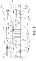
- FIG. 2 is a diagram illustrating a cross-sectional view of an EMI filter and electrostatic ESD / electrical surge protection device (device 200), which is an example implementation of the circuit 100a of FIG. 1B in the device 100a of FIG. 1A .
- the cross-sectional view of the device 200 in FIG. 2 corresponds with the section line C-C in FIG. 1A .
- the device 200 includes a very-heavily doped (e.g., n-type) substrate 260, and a lightly doped (e.g., p-type) semiconductor layer 265 disposed on the substrate 260.
- the semiconductor layer 265 can be an epitaxial semiconductor layer formed on the substrate 260.
- the device 200 also includes a plurality of dielectric layers 280 that are used as inter-layer dielectrics, e.g., for forming, or defining electrical contacts with circuit elements of the device 200.
- the dielectric layers 280 can include passivation layers, polyimide layers, oxide layers, etc.
- the device 200 includes an isolation region 210, an input terminal 216 (of an EMI filter circuit of the device 200), an isolation region 220, an output terminal 226 (of the EMI filter circuit), a ground region 230, a ground terminal 232, and an electrical connector 250.
- the isolation region 210 is defined by an isolation trench 212, while the isolation region 220 is defined by an isolation trench 222.
- the isolation trench 212 and the isolation trench 222 can be dielectric-filled (e.g., oxide-filled) trenches.
- the isolation trench 212 and the isolation trench 222 can each extend from a surface of the semiconductor layer 265, through the semiconductor layer 265 and terminate in the substrate 260. That is, the isolation trench 212 can isolate (electrically isolate) a portion of the semiconductor layer 265 within the isolation region 210 from portions of the semiconductor layer 265 outside the isolation region 210.
- the isolation trench 222 can isolate a portion of the semiconductor layer 265 within the isolation region 220 from portions of the semiconductor layer 265 outside the isolation region 220.
- the device 200 includes, within the isolation region 210, a diffusion region 270 (e.g., an n-type diffusion), and , within the isolation region 220, a diffusion region 275 (e.g., an n-type diffusion).
- the diffusion region 270 includes a region 270a disposed in the semiconductor layer 265, which can be a heavily-doped n-type region, and a region 270b disposed in the region 270a, which can be a very heavily-doped n-type region.
- the diffusion region 275 includes a region 275a disposed in the semiconductor layer 265, which can be a heavily-doped n-type region (N+), and a region 275b disposed in the region 275a, which can be a very heavily-doped n-type region (N++).
- the diffusion region 270 and the diffusion region 275 (and their respective regions) can be formed using ion implantation processes, or other semiconductor doping processes, such as well formation processes.
- an open-base bipolar transistor 214 is defined by the diffusion region 270, the portion of the semiconductor layer 265 within the isolation region 210, and the substrate 260. That is, a collector terminal of the open-base bipolar transistor 214 is included in the diffusion region 270, a base terminal of the open-base bipolar transistor 214 is included in the portion of the semiconductor layer 265 within the isolation region 210, and an emitter terminal of the open-base bipolar transistor 214 is included in the substrate 260.
- an open-base bipolar transistor 224 is defined by the diffusion region 275, the portion of the semiconductor layer 265 within the isolation region 220, and the substrate 260.
- a collector terminal of the open-base bipolar transistor 224 is included in the diffusion region 275
- a base terminal of the open-base bipolar transistor 224 is included in the portion of the semiconductor layer 265 within the isolation region 220
- an emitter terminal of the open-base bipolar transistor 224 is included in the substrate 260.
- a resistor 218 (diffusion resistor) is included in the diffusion region 270, while resistor 228 (diffusion resistor) is included in the diffusion region 275. That is, in this example, the diffusion region 270 includes (defines) the collector terminal of the open-base bipolar transistor 214 and the resistor 218, while the diffusion region 275 includes (defines) the collector terminal of the open-base bipolar transistor 224 and the resistor 228.
- the resistor 218 is electrically coupled in series with the resistor 228 (e.g., between the input terminal 216 and the output terminal 226) via the electrical connector 250, though that connection is not specifically shown in FIG. 2 due to the path of the section line C-C of FIG. 1A used to define the illustrated cross-sectional view of the device 200.
- the input terminal 216 includes a metal layer 216a, a metal layer 216b and a metal layer 216c to form an electrical connection to the diffusion region 270 (e.g., to the collector of the open-base bipolar transistor 214 and the resistor 218).
- the output terminal 226 includes a metal layer 226a, a metal layer 226b and a metal layer 226c to form an electrical connection to the diffusion region 275 (e.g., to the collector of the open-base bipolar transistor 224 and the resistor 228).
- the ground terminal 232 includes a metal layer 232a, a metal layer 232b and metal layer 232c, where the ground terminal 232 is electrically coupled with the substrate 260 (and a portion of the semiconductor layer 265 outside the isolation region 210 and outside the isolation region 220) via conductive trenches 232d.
- the metal layers 216a, 226a and 232a can include a tin-based solder material; the metal layers 216b, 226b and 232b can include copper; and the metal layers 216c, 226c and 232c can include an aluminum-copper alloy.
- other materials can be used for the metal layers, and fewer, or more metal layers can be included.
- the conductive trenches 232d can extend through a portion of the dielectric layers 280, through a surface of the 265, through the semiconductor layer 265, and terminate in the substrate 260.
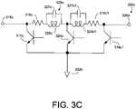
- FIGs. 3A through 3C are schematic diagrams of circuits that can be implemented, e.g., in the device of FIG. 1A , or variations of the device of FIG. 1A .
- the circuits of FIGs. 3A to 3C implement higher order EMI filters than the EMI filter of the circuit 100a.
- FIG. 3A illustrates a circuit 300 implementing a capacitive-resistive-inductive-capacitive (CRLC) filter
- FIG. 3B illustrates a circuit 300b implementing a CRCRC filter
- FIG. 3C illustrates a circuit 300c implementing a CRLC filter.
- 3A to 3B can be adjusted to tune performance of the associated EMI filters.
- respective values of impedance elements e.g., resistances, inductances and/or capacitances
- impedance elements can also be adjusted to tune performance of the corresponding EMI filters.
- the circuit 300a includes an open-base bipolar transistor 314a, and an open-base bipolar transistor 324a.
- respective base terminals of the open-base bipolar transistor 314a and the open-base bipolar transistor 324a can be electrically floating.
- an input terminal 316a can be electrically coupled with a collector terminal of the open-base bipolar transistor 314a
- an output terminal 326a can be electrically coupled with a collector terminal of the open-base bipolar transistor 324a.
- impedance elements of the EMI filter include a resistor 318a and an inductive-capacitive (LC) circuit (LC circuit 328a), which are electrically coupled in series between the input terminal 316a and the output terminal 326a.
- the LC circuit 328a includes a capacitor 327a that is electrically coupled in parallel with an inductor 329a.
- respective emitter terminals of the open-base bipolar transistor 314a and the open-base bipolar transistor 324a are electrically coupled with an electrical ground terminal 332a (corresponding with the electrical ground terminal 132 and the electrical ground terminal 142 of the device 100).
- the open-base bipolar transistor 314a and the resistor 318a can be included in a first isolation region, while the open-base bipolar transistor 324a and the LC circuit 328a can be included in a second isolation region.
- the circuit 300b includes an open-base bipolar transistor 314b, an open-base bipolar transistor 324b, and an open-base bipolar transistor 314b1.
- respective base terminals of the open-base bipolar transistor 314b, the open-base bipolar transistor 324b, and the open-base bipolar transistor 314b1 can be electrically floating.
- an input terminal 316b can be electrically coupled with a collector terminal of the open-base bipolar transistor 314b
- an output terminal 326b can be electrically coupled with a collector terminal of the open-base bipolar transistor 314b1.
- impedance elements of the EMI filter include a resistor 318b, a resistor 328b, a resistor 328b1, and a resistor 318b1, which are electrically coupled in series between the input terminal 316b and the output terminal 326b.
- a collector terminal of the open-base bipolar transistor 324b can be electrically coupled between the resistor 328b and the resistor 328b1.
- respective emitter terminals of the open-base bipolar transistor 314b, the open-base bipolar transistor 324b, and the open-base bipolar transistor 324b1 are electrically coupled with an electrical ground terminal 332b (corresponding with the electrical ground terminal 132 and the electrical ground terminal 142 of the device 100).
- the open-base bipolar transistor 314b and the resistor 318b can be included in a first isolation region.
- the open-base bipolar transistor 324b, the resistor 328b, and the resistor 328b1 can be included in a second isolation region.
- the open-base bipolar transistor 314b1 and the resistor 318b1 can be included in a third isolation region.
- the circuit 300c includes an open-base bipolar transistor 314c, an open-base bipolar transistor 324c, and an open-base bipolar transistor 314c1.
- respective base terminals of the open-base bipolar transistor 314c, the open-base bipolar transistor 324c, and the open-base bipolar transistor 314c1 can be electrically floating.
- an input terminal 316c can be electrically coupled with a collector terminal of the open-base bipolar transistor 314c
- an output terminal 326c can be electrically coupled with a collector terminal of the open-base bipolar transistor 314c1.
- impedance elements of the EMI filter include a resistor 318c, an LC circuit 328c, an LC circuit 328c1, and a resistor 318c1, which are electrically coupled in series between the input terminal 316c and the output terminal 326c.
- a collector terminal of the open-base bipolar transistor 324c can be electrically coupled between the LC circuit 328c and the LC circuit 328c1.
- the LC circuit 328c includes a capacitor 327c electrically coupled in parallel with an inductor 329c, while the LC circuit 328c1 includes a capacitor 327c1 electrically coupled in parallel with an inductor 329c1.
- respective emitter terminals of the open-base bipolar transistor 314c, the open-base bipolar transistor 324c, and the open-base bipolar transistor 314c1 are electrically coupled with an electrical ground terminal 332c (corresponding with the electrical ground terminal 132 and the electrical ground terminal 142 of the device 100).
- the open-base bipolar transistor 314c and the resistor 318c can be included in a first isolation region.
- the open-base bipolar transistor 324c, the LC circuit 328c, and the LC circuit 328c1 can be included in a second isolation region.
- the open-base bipolar transistor 314c1 and the resistor 318c1 can be included in a third isolation region.
- FIG. 4 is a diagram illustrating operation of the device 200 of FIG. 2 (e.g., the circuit 100a) during an electrostatic discharge (or electrical surge) event 400 occurring on the input terminal 216.
- FIG. 4 is given by way of example, and the device 200 can operate similarly in response to other ESD or electrical surge events, such as events occurring on the output terminal 226, where the 224 can act as a voltage clamp.
- the 214 in response to the event 400 on the input terminal 216, the 214 can act a voltage clamp and conduct a current 410 associated with the event 400, which can be a majority of the current associated with the event 400.
- the current 410 in this example can be conducted from the input terminal 216, through the open-base bipolar transistor 214 (operating in breakdown), through the substrate 260, and to the ground terminal 232 through the conductive trenches 232d.
- a residual current 420 associated with the event 400 can be conducted by the resistor 218 (and the resistor 228).
- the open-base bipolar transistor 214 acts as a voltage clamp
- the open-base bipolar transistor 214 and the resistor 218 are included in the isolation region 210, and there is a low resistance, and low inductance conductive path to the ground terminal 232, current (current 410 and current 420) from the event 400 can be efficiently conducted, preventing damage to the device.
- clamping voltage of an open-base bipolar in response to an ESD or electrical surge event can be adjusted based on design and/or processing parameters. For instance, in described implementations, clamping voltage of an open-base bipolar depends on a breakdown voltage (V br ) of the open-base bipolar and current through the open-base bipolar.
- V br breakdown voltage
- Vbr of the open-base bipolar e.g., to a value greater than an upper operating voltage limit, as well as adjusting dynamic resistance (R dyn ), e.g., by varying a size of the open base-bipolar and/or process
- V clamp a desired clamping voltage
- I a current conducted through the open-base bipolar, e.g., a current associated with a given ESD or electrical surge event.
- FIG. 5 is a diagram illustrating aspects of the device 200 of FIG. 2 (e.g., the circuit 100a) for filtering EMI.
- circuit elements of the device 200 within the isolation region 210 are described by way of example.
- like circuit elements within the isolation region 220 are not described herein, as those elements can implement aspects for implementing EMI filtering that correspond with the aspects described below with respect to the circuit elements included in the isolation region 210.
- junction capacitances of the open-base bipolar transistor 214 can be included in an EMI filter of the device 200. These junction capacitances can include a collector-to-base capacitance (C CB ) of the open-base bipolar transistor 214, and a base-to-emitter capacitance (C BE ) of the open-base bipolar transistor 214. Additionally, distributed junction capacitance (C R ) of the resistor 218 can also be included in the EMI filter. In implementations, C CB , C BE , and C R can be adjusted (e.g., by layout, sizing, doping concentrations, etc.) to achieve desired linearity of the associated EMI filter.
- these capacitances can be adjusted such that they are symmetrical, where the combined capacitance of C CB and C R matches (is equal to, or approximately equal to) C BE .
- Such an approach can provide linear operation of the associated EMI filter, which allows for attenuation of a fundamental RF frequency (f 0 ) that can be coupled (via EMI) onto a data path of the device (e.g., between the input terminal 216 and the 226), as well attenuation harmonics of f 0 .
- Such harmonics can include a second harmonic (f 2 ) and a third harmonic (f 3 ).
- Operation of the EMI filter can also be tuned by adjusting a relationship between capacitances (e.g, C CB , C BE , and C R ) and impedances (e.g., resistance of the resistor 218 and the resistor 228), such as to achieve a desired cutoff frequency of the EMI filter.
- capacitances e.g, C CB , C BE , and C R
- impedances e.g., resistance of the resistor 218 and the resistor 2248
- low resistance and low inductance of the electrical ground connection e.g., between the substrate 260 and the ground terminal 232
- R SUB 560 low resistance
- a cutoff frequency of 65 megahertz (MHz) (above a data rate for digital data communicated by the EMI filter) can be achieved.
- attenuation of f 0 e.g., greater than 700 MHz
- filtering of f 2 e.g., greater than 1.4 gigahertz (GHz)
- filtering of f 3 e.g., greater than 2.1 GHz
- the various apparatus and techniques described herein may be implemented using various semiconductor processing and/or packaging techniques. Some implementations may be implemented using various types of semiconductor processing techniques associated with semiconductor substrates including, but not limited to, for example, Silicon (Si), Gallium Arsenide (GaAs), Silicon Carbide (SiC), and/or so forth.
- semiconductor substrates including, but not limited to, for example, Silicon (Si), Gallium Arsenide (GaAs), Silicon Carbide (SiC), and/or so forth.
- a singular form may, unless definitely indicating a particular case in terms of the context, include a plural form.
- Spatially relative terms e.g., over, above, upper, under, beneath, below, lower, and so forth
- the relative terms above and below can, respectively, include vertically above and vertically below.
- the term adjacent can include laterally adjacent to or horizontally adjacent to.
Landscapes
- Engineering & Computer Science (AREA)
- Microelectronics & Electronic Packaging (AREA)
- Semiconductor Integrated Circuits (AREA)
- Physics & Mathematics (AREA)
- Health & Medical Sciences (AREA)
- Electromagnetism (AREA)
- Toxicology (AREA)
Abstract
Description
- This disclosure relates to circuits, such as circuits that can be implemented in a semiconductor device. More specifically, this disclosure relates to circuits and devices for providing linear electromagnetic interference filtering, as well as protection from electrostatic discharge and/or electrical surge events.
- Semiconductor processing technologies, and related packaging technologies continue to scale to smaller dimensions. Additionally, semiconductor devices produced using such technologies can be included in systems with increased performance requirements, such as speed of operation. For instance, electromagnetic interference (EMI) filter devices implemented in mobile device technologies, such as fifth-generation (5G) wireless technologies, can be subjected to increasing EMI levels, e.g., due to increased radio frequency (RF) of operation and/or additional antennas being added, as compared to previous devices. Furthermore, scaling to smaller technologies also presents challenges in meeting electrostatic discharge (ESD) and electrical (voltage and/or current) surge protection target specifications. Current protection approaches cannot achieve sufficient ESD and electrical surge protection, while maintaining desired linearity and EMI attenuation performance in such EMI filter devices.
- In some aspects, the techniques described herein relate to an electromagnetic interference (EMI) filter circuit including: an input terminal; an output terminal; an electrical ground terminal; a resistor electrically coupled between the input terminal and the output terminal; a first bipolar transistor including: a collector terminal electrically coupled with the input terminal; an emitter terminal electrically coupled with the electrical ground terminal; and a base terminal that is electrically floating; and a second bipolar transistor including: a collector terminal electrically coupled with the output terminal; an emitter terminal electrically coupled with the electrical ground terminal; and a base terminal that is electrically floating.
- In some aspects, the techniques described herein relate to a EMI filter circuit, wherein the resistor is a first resistor, the EMI filter circuit further including: a second resistor electrically coupled in series with the first resistor between the input terminal and the output terminal; and a third bipolar transistor including: a collector terminal electrically coupled between the first resistor and the second resistor; an emitter terminal electrically coupled with the electrical ground terminal; and a base terminal that is electrically floating.
- In some aspects, the techniques described herein relate to a EMI filter circuit, wherein: the EMI filter circuit is included in a semiconductor device; the first bipolar transistor is a first vertical bipolar transistor; the second bipolar transistor is a second vertical bipolar transistor; and the third bipolar transistor is a third vertical bipolar transistor.
- In some aspects, the techniques described herein relate to a EMI filter circuit, further including: an inductive-capacitive (LC) circuit including: an inductor; and a capacitor electrically coupled in parallel with the inductor, the LC circuit being electrically coupled in series with the resistor between the input terminal and the output terminal.
- In some aspects, the techniques described herein relate to a EMI filter circuit, wherein the resistor is a first resistor and the LC circuit is a first LC circuit, the EMI filter circuit further including: a second resistor; and a second LC circuit, the first resistor, the first LC circuit, the second LC circuit, and the second resistor being electrically coupled in series between the input terminal and the output terminal, the EMI filter circuit further including: a third bipolar transistor including: a collector terminal electrically coupled between the first LC circuit and the second LC circuit; an emitter terminal electrically coupled with the electrical ground terminal; and a base terminal that is electrically floating.
- In some aspects, the techniques described herein relate to a EMI filter circuit, wherein the resistor is a first resistor, the EMI filter circuit further including: a second resistor electrically coupled in series with the first resistor between the input terminal and the output terminal.
- In some aspects, the techniques described herein relate to a EMI filter circuit, wherein: the EMI filter circuit is included in a semiconductor device; the first bipolar transistor is a first vertical bipolar transistor; the first resistor is a first diffusion resistor; the second bipolar transistor is a second vertical bipolar transistor; and the second resistor is a second diffusion resistor.
- In some aspects, the techniques described herein relate to a semiconductor device including: a substrate of a first conductivity type; a semiconductor layer of a second conductivity type that is opposite the first conductivity type; a first isolation region defined by a first trench; a first diffusion region of the first conductivity type disposed in the semiconductor layer in the first isolation region; a second isolation region defined by a second trench; a second diffusion region of the first conductivity type disposed in the semiconductor layer in the second isolation region; an electrical ground terminal disposed on the semiconductor layer outside the first isolation region and outside the second isolation region; and an electromagnetic interference (EMI) filter circuit including: an input terminal disposed on the semiconductor layer in the first isolation region; an output terminal disposed on the semiconductor layer in the second isolation region; a first electrical impedance element disposed in the first isolation region; a second electrical impedance element disposed in the second isolation region, the first electrical impedance element and the second electrical impedance element being electrically coupled in series between the input terminal and the output terminal; a first vertical bipolar transistor disposed in the first isolation region, the first vertical bipolar transistor including: a collector terminal electrically coupled with the input terminal; an emitter terminal electrically coupled with the electrical ground terminal; and a base terminal that is electrically floating; and a second vertical bipolar transistor disposed in the second isolation region, the second vertical bipolar transistor including: a collector terminal electrically coupled with the output terminal; an emitter terminal electrically coupled with the electrical ground terminal; and a base terminal that is electrically floating.
- In some aspects, the techniques described herein relate to a semiconductor device, wherein: the first trench extends from an upper surface of the semiconductor layer, through the semiconductor layer and terminates in the substrate, the first trench having a dielectric material disposed therein; and the second trench extends from the upper surface of the semiconductor layer, through the semiconductor layer and terminates in the substrate, the second trench having the dielectric material disposed therein.
- In some aspects, the techniques described herein relate to a semiconductor device, wherein the electrical ground terminal is electrically coupled with the substrate via a plurality of trenches filled with an electrically conductive material.
- In some aspects, the techniques described herein relate to a semiconductor device, wherein the plurality of trenches extend from a surface of the semiconductor layer, through the semiconductor layer and terminate in the substrate.
- In some aspects, the techniques described herein relate to a semiconductor device, wherein: the first electrical impedance element is a first diffusion resistor included in the first diffusion region; and the second electrical impedance element is a second diffusion resistor included in the second diffusion region.
- In some aspects, the techniques described herein relate to a semiconductor device, wherein: the collector terminal of the first vertical bipolar transistor is included in the first diffusion region; the base terminal of the first vertical bipolar transistor is included in the semiconductor layer; the emitter terminal of the first vertical bipolar transistor is included in the substrate; the collector terminal of the second vertical bipolar transistor is included in the second diffusion region; the base terminal of the second vertical bipolar transistor is included in the semiconductor layer; and the emitter terminal of the second vertical bipolar transistor is included in the substrate.
- In some aspects, the techniques described herein relate to a semiconductor device, wherein: the first electrical impedance element is a resistor; and the second electrical impedance element is an inductive-capacitive (LC) circuit.
- In some aspects, the techniques described herein relate to a semiconductor device, wherein the first diffusion region includes: a first region disposed in the semiconductor layer, the first region having a first doping concentration; and a second region disposed in the first region, the second region having a second doping concentration that is greater than the first doping concentration.
- In some aspects, the techniques described herein relate to a semiconductor device, wherein: the first conductivity type is n-type; and the second conductivity type is p-type.
- In some aspects, the techniques described herein relate to a method including: receiving an electrical transient at one of an input terminal, an output terminal, or an electrical ground terminal of an electromagnetic interference (EMI) filter circuit; clamping a voltage of the electrical transient with a vertical, open-base bipolar transistor of the EMI filter circuit; conducting a first portion of a current of the electrical transient with the vertical, open-base bipolar transistor; and conducting a second portion of the current of the electrical transient with an electrical impedance element of the EMI filter circuit, the second portion of the current being less than the first portion of the current, a collector terminal of the vertical, open-base bipolar transistor being electrically coupled with one of the input terminal or the output terminal, an emitter terminal of the vertical, open-base bipolar transistor being electrically coupled with the electrical ground terminal, and the electrical impedance element being electrically coupled between the input terminal and the output terminal.
- In some aspects, the techniques described herein relate to a method, wherein the electrical transient is one of an electrostatic discharge (ESD) or an electrical surge.
- In some aspects, the techniques described herein relate to a method, wherein the electrical impedance element includes at least one of a diffusion resistor or an inductive-capacitive circuit.
- In some aspects, the techniques described herein relate to a method, wherein the vertical, open-base bipolar transistor and the electrical impedance element are included in an isolation region of the EMI filter circuit.
-
-
FIG. 1A is a block diagram schematically illustrating an electromagnetic interference (EMI) filter and electrostatic discharge (ESD) / electrical surge protection device. -
FIG. 1B is a schematic diagram illustrating a circuit that can be implemented in the device ofFIG. 1A . -
FIG. 2 is a diagram illustrating a cross-sectional view of an implementation of the circuit ofFIG. 1B in the device ofFIG. 1A . -
FIGs. 3A through 3C are schematic diagrams of circuits that can be implemented, e.g., in the device ofFIG. 1A , or variations of the device ofFIG. 1A . -
FIG. 4 is a diagram illustrating operation of the device ofFIG. 2 during an ESD (or electrical surge) event. -
FIG. 5 is a diagram illustrating aspects of the device ofFIG. 2 for filtering EMI. - In the drawings, which are not necessarily drawn to scale, like reference symbols may indicate like and/or similar components (elements, structures, etc.) in different views. The drawings illustrate generally, by way of example, but not by way of limitation, various implementations discussed in the present disclosure. Reference symbols show in one drawing may not be repeated for the same, and/or similar elements in related views. Reference symbols that are repeated in multiple drawings may not be specifically discussed with respect to each of those drawings, but are provided for context between related views. Also, not all like elements in the drawings are specifically referenced with a reference symbol when multiple instances of that element are illustrated.
- In the following detailed description (and in the accompanying drawings) a number of example implementations of electromagnetic interference (EMI) filter and electrostatic discharge (ESD) / electrical surge protection devices (and their operation) are described and illustrated. The illustrated devices include a number of similar aspects, as well as a number of variations from one illustrated implementation to another. In the implementations disclosed herein, an EMI filter of such a device can include active, open-base bipolar transistors and electrical impedance elements (e.g., resistors, capacitors, and/or inductors) that provide for linear filtering of EMI that can occur as a result of radio frequency noise, as well as associated harmonics, that can be wirelessly coupled onto an associated data path and/or can occur due to non-linearity of the EMI filter, where the data path is configured to communicate digital information (data) associated with operation of a corresponding wireless communication device (e.g., a mobile phone, etc.), e.g., at frequencies that are more than an order of magnitude lower than radio frequencies. For instance, collector-to-base capacitances, base-to emitter capacitances and/or distributed capacitances of the electrical impedance elements can be adjusted to achieved desired EMI filtering (e.g., linearity and attenuation) performance.
- In the example implementations described herein, the open-base bipolar transistors and electrical impedance elements can be included in (disposed in, etc.) respective isolation regions in a semiconductor device. In such approaches, the isolated open-base bipolar transistors and electrical impedance elements can, in addition to providing for EMI filtering, prevent damage to the EMI filter device from ESD and/or electrical surge (e.g., over-current and/or overvoltage) events. As noted above, EMI filtering performance of example implementations can be tuned by adjusting junction capacitances of the open-base bipolar transistors and/or distributed capacitances of the electrical impedance elements, e.g., by adjusting doping concentrations, and/or adjusting layout and sizing of the circuit elements of the EMI filter, and so forth. EMI filter performance can also be adjusted (tuned) by adjusting impedances of impedance elements included in the EMI filter (e.g., using similar techniques as those for adjusting capacitances).
- In the examples described herein, one or more aspects of one implementation can be likewise implemented in one or more other implementations. For instance, arrangement and relative sizes of implants, specific circuit elements, etc., shown in one example implementation could also be implemented in other implementations. In some implementations, circuit elements (e.g., transistors, resistors, capacitors, inductors) can be added to, substituted for, or removed.
- Additionally, example devices and circuits are described herein as being implemented with specific conductivity types (e.g., n-type or p-type) for specific implants and/or regions (e.g., diffusion regions). The doping concentrations of each of these implants and/or regions can vary based on the particular implementation. For purposes of illustration, and by way of example, in certain instances, qualitative examples of doping concentration (e.g., lightly doped, heavily doped, very-heavily doped, and so forth) are given. In the described examples, these qualitative indications of doping concentration are relative. That is, as used herein, lightly doped indicates lower doping concentration than heavily doped, while heavily doped indicates lower doping concentration than very-heavily doped. Specific, quantitative doping concentrations associated with these qualitative doping concentrations can vary based on the particular implementation. Further, in some implementations, the conductivity types of the various regions described herein can be inverted. That is, regions of the example devices described as being n-type can be implemented as p-type, and regions described as being p-type can be implemented as n-type, NPN transistors can be implemented as PNP transistors, etc.
-
FIG. 1A is a block diagram schematically illustrating an example EMI filter and ESD / electrical surge protection device (e.g., device 100). As shown inFIG. 1A , thedevice 100 includes anisolation region 110, anisolation region 120, anelectrical ground region 130, anelectrical ground region 140, and anelectrical interconnection 150. In some implementations, portions of thedevice 100 can be replicated and/or mirrored to create devices that implement higher order filters, such as the examples shown inFIGs. 3A to 3C . - As shown in
FIG. 1A , theisolation region 110 is defined by anisolation trench 112, which can be a dielectric filled trench. Similarly, theisolation region 120 is defined by anisolation trench 122, which can also be a dielectric filled trench. Thedevice 100 can include circuit elements that are respectively implemented in theisolation region 110 and theisolation region 120. In implementations, these circuit elements can be configured to implement an EMI filter circuit, as well as to provide ESD and electrical surge protection for thedevice 100. For instance, as shown inFIG. 1A , a transistor 114 (e.g., a vertical, bipolar transistor) and anelectrical impedance element 118 can be implemented in theisolation region 110, while a transistor 124 (e.g., a vertical, bipolar transistor) and anelectrical impedance element 128 can be implemented in theisolation region 120. A signal pad (e.g., an input terminal 116) of the corresponding EMI filter circuit can also be included in theisolation region 110, while a signal pad (e.g., an output terminal 126) of the corresponding EMI filter circuit can be included in theisolation region 120. In implementations, theelectrical impedance element 118 and theelectrical impedance element 128 can respectively include resistors, inductors and/or capacitors, such as in the examples described herein. The specific circuit elements of thedevice 100 will depend on the particular implementation. - In the
device 100, theground region 130 and the ground region 140 (which are both outside theisolation region 110 and outside the isolation region 120) can each include a plurality of conductive trenches, e.g., arrays of trenches filled with an electrically conductive material, such as tungsten. The conductive trenches, such as those illustrated inFIG. 2 , can electrically couple, respectively, an electrical ground terminal 132 (e.g., signal pad) of theelectrical ground region 130 and an electrical ground terminal 142 (e.g., signal pad) of theelectrical ground region 140 with a semiconductor substrate of thedevice 100. That is, such conductive trenches can provide low resistance, and low inductance electrical connections from theelectrical ground terminal 132 and the electrical ground terminal 142 to an associated semiconductor substrate, so as to reduce adverse impacts on linearity and attenuation performance of the corresponding EMI filter circuit due to electrical impedance (e.g., resistance and inductance) of the electrical ground connections. As also shown inFIG. 1A , theelectrical interconnection 150, in this example, electrically couples theelectrical impedance element 118 with theelectrical impedance element 128. -
FIG. 1A also includes a section line C-C, which corresponds with the cross-sectional view shown inFIG. 2 . As shown inFIG. 1A , the section line C-C extends through theisolation region 110, through theelectrical ground region 130, and through theisolation region 120. That is, the section line C-C is not a straight line, such that theisolation region 110, theelectrical ground region 130 and theisolation region 120 of the device 100 (and their corresponding regions inFIG. 2 ) are included the cross-section defined by the section line C-C. -
FIG. 1 B is a schematic diagram illustrating an EMI filter and electrostatic ESD / electrical surge protection circuit (circuit 100a) that can be implemented in thedevice 100 ofFIG. 1A . For purposes of illustration, elements of thecircuit 100a corresponding with elements of thedevice 100 are referenced with like 100 series reference numbers suffixed with the letter 'a.' In other implementations, elements of thecircuit 100a can be replaced with other elements, additional elements can be added, and/or elements can be removed. - In the example of
FIG. 1B , thecircuit 100a includes an open-basebipolar transistor 114a, and an open-basebipolar transistor 124a. For instance, in thecircuit 100a, respective base terminals of the open-basebipolar transistor 114a and the open-basebipolar transistor 124a can be electrically floating. Further in thecircuit 100a, aninput terminal 116a can be electrically coupled with a collector terminal of the open-basebipolar transistor 114a, while anoutput terminal 126a can be electrically coupled with a collector terminal of the open-basebipolar transistor 124a. Also in thecircuit 100a, aresistor 118a and aresistor 128a can be electrically coupled in series between theinput terminal 116a and theoutput terminal 126a, where theresistor 118a is electrically coupled with theresistor 128a via anelectrical connector 150a. As shown inFIG. 1B , respective emitter terminals of the open-basebipolar transistor 114a and the open-basebipolar transistor 124a are electrically coupled with anelectrical ground terminal 132a/142a (corresponding with theelectrical ground terminal 132 and the electrical ground terminal 142 of the device 100). - In this example, the
circuit 100a implements a capacitive-resistive- capacitive (CRC) EMI filter. For instance, junction capacitances (e.g., collector-to-base and base-to-emitter capacitances) of the open-basebipolar transistor 114a and the open-basebipolar transistor 124a can provide capacitive elements of the EMI filter, while theresistor 118a and theresistor 128a can provide resistive elements of the EMI filter. Further, in implementations where theresistor 118a and theresistor 128a are implemented as diffusion resistors, respective distributed junction capacitances of theresistor 118a and theresistor 128a can also provide additional capacitive elements of the EMI filter of thecircuit 100a. Desired EMI filtering performance (e.g., cutoff frequency, linearity, attenuation, etc.) of the 100a can be achieved by adjusting, respectively, capacitance and/or resistance of these elements. For instance, in semiconductor device (e.g., integrated circuit) implementations of thecircuit 100a, capacitance and/or resistance can be adjusted (tuned) through layout, including sizing, relative doping concentrations, etc. of the elements of thecircuit 100a. Additional aspects of EMI filtering by an example implementation of thecircuit 100a (e.g., the implementation ofFIG. 2 ) are further described below with respect to, at least,FIG. 5 . - Further in the example of
FIG. 1B , the open-basebipolar transistor 114a, the open-basebipolar transistor 124a, theresistor 118a, and theresistor 128a, in addition to implementing EMI filtering, can also protect thecircuit 100a from damage associated with ESD and/or electrical surge events. For instance, in response to an ESD or electrical surge event, the open-basebipolar transistor 114a, and/or the open-basebipolar transistor 124a can act as a voltage clamp (e.g., at an associated breakdown voltage), and shunt a majority of current associated with the ESD or electrical surge event to theelectrical ground terminal 132a/142a. In this example, any residual current associated with the ESD or electrical surge event can be conducted via theresistor 118a and theresistor 128a, e.g., at a current density below a level that can damage theresistor 118a or theresistor 128a. Additional aspects of the operation of an example implementation of thecircuit 100a (e.g., the implementation ofFIG. 2 ) during an ESD or electric surge event are further described below with respect to, at least,FIG. 4 . -
FIG. 2 is a diagram illustrating a cross-sectional view of an EMI filter and electrostatic ESD / electrical surge protection device (device 200), which is an example implementation of thecircuit 100a ofFIG. 1B in thedevice 100a ofFIG. 1A . As discussed above, the cross-sectional view of thedevice 200 inFIG. 2 corresponds with the section line C-C inFIG. 1A . As shown inFIG. 2 , thedevice 200 includes a very-heavily doped (e.g., n-type)substrate 260, and a lightly doped (e.g., p-type)semiconductor layer 265 disposed on thesubstrate 260. In some implementations, thesemiconductor layer 265 can be an epitaxial semiconductor layer formed on thesubstrate 260. Thedevice 200 also includes a plurality ofdielectric layers 280 that are used as inter-layer dielectrics, e.g., for forming, or defining electrical contacts with circuit elements of thedevice 200. In some implementations, thedielectric layers 280 can include passivation layers, polyimide layers, oxide layers, etc. - For purposes of illustration and comparison with
FIGs. 1A and 1B , elements of thedevice 200 corresponding with elements of thedevice 100 and/or thecircuit 100a, are referenced with like 200 series reference numbers. For instance, thedevice 200 includes anisolation region 210, an input terminal 216 (of an EMI filter circuit of the device 200), anisolation region 220, an output terminal 226 (of the EMI filter circuit), aground region 230, aground terminal 232, and anelectrical connector 250. - As shown in
FIG. 2 , theisolation region 210 is defined by anisolation trench 212, while theisolation region 220 is defined by anisolation trench 222. Theisolation trench 212 and theisolation trench 222 can be dielectric-filled (e.g., oxide-filled) trenches. As shown inFIG. 2 , theisolation trench 212 and theisolation trench 222 can each extend from a surface of thesemiconductor layer 265, through thesemiconductor layer 265 and terminate in thesubstrate 260. That is, theisolation trench 212 can isolate (electrically isolate) a portion of thesemiconductor layer 265 within theisolation region 210 from portions of thesemiconductor layer 265 outside theisolation region 210. Likewise, theisolation trench 222 can isolate a portion of thesemiconductor layer 265 within theisolation region 220 from portions of thesemiconductor layer 265 outside theisolation region 220. - In this example, the
device 200 includes, within theisolation region 210, a diffusion region 270 (e.g., an n-type diffusion), and , within theisolation region 220, a diffusion region 275 (e.g., an n-type diffusion). Thediffusion region 270 includes aregion 270a disposed in thesemiconductor layer 265, which can be a heavily-doped n-type region, and aregion 270b disposed in theregion 270a, which can be a very heavily-doped n-type region. Likewise, thediffusion region 275 includes aregion 275a disposed in thesemiconductor layer 265, which can be a heavily-doped n-type region (N+), and aregion 275b disposed in theregion 275a, which can be a very heavily-doped n-type region (N++). In some implementations, thediffusion region 270 and the diffusion region 275 (and their respective regions) can be formed using ion implantation processes, or other semiconductor doping processes, such as well formation processes. - As shown in
FIG. 2 , an open-base bipolar transistor 214 (NPN transistor) is defined by thediffusion region 270, the portion of thesemiconductor layer 265 within theisolation region 210, and thesubstrate 260. That is, a collector terminal of the open-basebipolar transistor 214 is included in thediffusion region 270, a base terminal of the open-basebipolar transistor 214 is included in the portion of thesemiconductor layer 265 within theisolation region 210, and an emitter terminal of the open-basebipolar transistor 214 is included in thesubstrate 260. Similarly, an open-base bipolar transistor 224 (NPN transistor) is defined by thediffusion region 275, the portion of thesemiconductor layer 265 within theisolation region 220, and thesubstrate 260. That is, a collector terminal of the open-basebipolar transistor 224 is included in thediffusion region 275, a base terminal of the open-basebipolar transistor 224 is included in the portion of thesemiconductor layer 265 within theisolation region 220, and an emitter terminal of the open-basebipolar transistor 224 is included in thesubstrate 260. - In the
device 200, a resistor 218 (diffusion resistor) is included in thediffusion region 270, while resistor 228 (diffusion resistor) is included in thediffusion region 275. That is, in this example, thediffusion region 270 includes (defines) the collector terminal of the open-basebipolar transistor 214 and theresistor 218, while thediffusion region 275 includes (defines) the collector terminal of the open-basebipolar transistor 224 and theresistor 228. In this example, theresistor 218 is electrically coupled in series with the resistor 228 (e.g., between theinput terminal 216 and the output terminal 226) via theelectrical connector 250, though that connection is not specifically shown inFIG. 2 due to the path of the section line C-C ofFIG. 1A used to define the illustrated cross-sectional view of thedevice 200. - As illustrated in
FIG. 2 , theinput terminal 216 includes ametal layer 216a, ametal layer 216b and ametal layer 216c to form an electrical connection to the diffusion region 270 (e.g., to the collector of the open-basebipolar transistor 214 and the resistor 218). Further in thedevice 200, theoutput terminal 226 includes ametal layer 226a, ametal layer 226b and ametal layer 226c to form an electrical connection to the diffusion region 275 (e.g., to the collector of the open-basebipolar transistor 224 and the resistor 228). Theground terminal 232 includes ametal layer 232a, ametal layer 232b andmetal layer 232c, where theground terminal 232 is electrically coupled with the substrate 260 (and a portion of thesemiconductor layer 265 outside theisolation region 210 and outside the isolation region 220) viaconductive trenches 232d. In some implementations, themetal layers metal layers metal layers FIG. 2 , theconductive trenches 232d can extend through a portion of thedielectric layers 280, through a surface of the 265, through thesemiconductor layer 265, and terminate in thesubstrate 260. -
FIGs. 3A through 3C are schematic diagrams of circuits that can be implemented, e.g., in the device ofFIG. 1A , or variations of the device ofFIG. 1A . The circuits ofFIGs. 3A to 3C implement higher order EMI filters than the EMI filter of thecircuit 100a. Specifically,FIG. 3A illustrates a circuit 300 implementing a capacitive-resistive-inductive-capacitive (CRLC) filter,FIG. 3B illustrates acircuit 300b implementing a CRCRC filter, andFIG. 3C illustrates acircuit 300c implementing a CRLC filter. As with the other example implementations described herein, junction capacitances of elements of the circuits inFIGs. 3A to 3B (e.g., of open-base bipolar transistors and/or impedance elements) can be adjusted to tune performance of the associated EMI filters. Also, respective values of impedance elements (e.g., resistances, inductances and/or capacitances) can also be adjusted to tune performance of the corresponding EMI filters. - Referring to
FIG. 3A , thecircuit 300a includes an open-basebipolar transistor 314a, and an open-basebipolar transistor 324a. In thecircuit 300a, respective base terminals of the open-basebipolar transistor 314a and the open-basebipolar transistor 324a can be electrically floating. Further in thecircuit 300a, aninput terminal 316a can be electrically coupled with a collector terminal of the open-basebipolar transistor 314a, while anoutput terminal 326a can be electrically coupled with a collector terminal of the open-basebipolar transistor 324a. In thecircuit 300a, impedance elements of the EMI filter include aresistor 318a and an inductive-capacitive (LC) circuit (LC circuit 328a), which are electrically coupled in series between theinput terminal 316a and theoutput terminal 326a. TheLC circuit 328a includes acapacitor 327a that is electrically coupled in parallel with aninductor 329a. As shown inFIG. 3A , respective emitter terminals of the open-basebipolar transistor 314a and the open-basebipolar transistor 324a are electrically coupled with anelectrical ground terminal 332a (corresponding with theelectrical ground terminal 132 and the electrical ground terminal 142 of the device 100). In thecircuit 300a, the open-basebipolar transistor 314a and theresistor 318a can be included in a first isolation region, while the open-basebipolar transistor 324a and theLC circuit 328a can be included in a second isolation region. - Referring to
FIG. 3B , thecircuit 300b includes an open-basebipolar transistor 314b, an open-basebipolar transistor 324b, and an open-base bipolar transistor 314b1. In thecircuit 300b, respective base terminals of the open-basebipolar transistor 314b, the open-basebipolar transistor 324b, and the open-base bipolar transistor 314b1 can be electrically floating. Further in thecircuit 300b, aninput terminal 316b can be electrically coupled with a collector terminal of the open-basebipolar transistor 314b, and anoutput terminal 326b can be electrically coupled with a collector terminal of the open-base bipolar transistor 314b1. In thecircuit 300a, impedance elements of the EMI filter include aresistor 318b, aresistor 328b, a resistor 328b1, and a resistor 318b1, which are electrically coupled in series between theinput terminal 316b and theoutput terminal 326b. A collector terminal of the open-basebipolar transistor 324b can be electrically coupled between theresistor 328b and the resistor 328b1. - As shown in
FIG. 3B , respective emitter terminals of the open-basebipolar transistor 314b, the open-basebipolar transistor 324b, and the open-base bipolar transistor 324b1 are electrically coupled with anelectrical ground terminal 332b (corresponding with theelectrical ground terminal 132 and the electrical ground terminal 142 of the device 100). In thecircuit 300b, the open-basebipolar transistor 314b and theresistor 318b can be included in a first isolation region. The open-basebipolar transistor 324b, theresistor 328b, and the resistor 328b1 can be included in a second isolation region. The open-base bipolar transistor 314b1 and the resistor 318b1 can be included in a third isolation region. - Referring to
FIG. 3C , thecircuit 300c includes an open-basebipolar transistor 314c, an open-basebipolar transistor 324c, and an open-base bipolar transistor 314c1. In thecircuit 300c, respective base terminals of the open-basebipolar transistor 314c, the open-basebipolar transistor 324c, and the open-base bipolar transistor 314c1 can be electrically floating. Further in thecircuit 300c, aninput terminal 316c can be electrically coupled with a collector terminal of the open-basebipolar transistor 314c, and anoutput terminal 326c can be electrically coupled with a collector terminal of the open-base bipolar transistor 314c1. In thecircuit 300a, impedance elements of the EMI filter include aresistor 318c, anLC circuit 328c, an LC circuit 328c1, and a resistor 318c1, which are electrically coupled in series between theinput terminal 316c and theoutput terminal 326c. A collector terminal of the open-basebipolar transistor 324c can be electrically coupled between theLC circuit 328c and the LC circuit 328c1. TheLC circuit 328c includes acapacitor 327c electrically coupled in parallel with aninductor 329c, while the LC circuit 328c1 includes a capacitor 327c1 electrically coupled in parallel with an inductor 329c1. - As shown in
FIG. 3C , respective emitter terminals of the open-basebipolar transistor 314c, the open-basebipolar transistor 324c, and the open-base bipolar transistor 314c1 are electrically coupled with anelectrical ground terminal 332c (corresponding with theelectrical ground terminal 132 and the electrical ground terminal 142 of the device 100). In thecircuit 300c, the open-basebipolar transistor 314c and theresistor 318c can be included in a first isolation region. The open-basebipolar transistor 324c, theLC circuit 328c, and the LC circuit 328c1 can be included in a second isolation region. The open-base bipolar transistor 314c1 and the resistor 318c1 can be included in a third isolation region. -
FIG. 4 is a diagram illustrating operation of thedevice 200 ofFIG. 2 (e.g., thecircuit 100a) during an electrostatic discharge (or electrical surge)event 400 occurring on theinput terminal 216.FIG. 4 is given by way of example, and thedevice 200 can operate similarly in response to other ESD or electrical surge events, such as events occurring on theoutput terminal 226, where the 224 can act as a voltage clamp. - As shown in
FIG. 4 , in response to theevent 400 on theinput terminal 216, the 214 can act a voltage clamp and conduct a current 410 associated with theevent 400, which can be a majority of the current associated with theevent 400. The current 410, in this example can be conducted from theinput terminal 216, through the open-base bipolar transistor 214 (operating in breakdown), through thesubstrate 260, and to theground terminal 232 through theconductive trenches 232d. As also shown inFIG. 4 , a residual current 420 associated with theevent 400 can be conducted by the resistor 218 (and the resistor 228). In this example, because the open-basebipolar transistor 214 acts as a voltage clamp, the open-basebipolar transistor 214 and theresistor 218 are included in theisolation region 210, and there is a low resistance, and low inductance conductive path to theground terminal 232, current (current 410 and current 420) from theevent 400 can be efficiently conducted, preventing damage to the device. - In some implementations, clamping voltage of an open-base bipolar (such as those described herein) in response to an ESD or electrical surge event can be adjusted based on design and/or processing parameters. For instance, in described implementations, clamping voltage of an open-base bipolar depends on a breakdown voltage (Vbr) of the open-base bipolar and current through the open-base bipolar. Thus by adjusting Vbr of the open-base bipolar, e.g., to a value greater than an upper operating voltage limit, as well as adjusting dynamic resistance (Rdyn), e.g., by varying a size of the open base-bipolar and/or process, a desired clamping voltage (Vclamp) can be achieved, where is given by Vclamp = Rdyn ∗I, and I is a current conducted through the open-base bipolar, e.g., a current associated with a given ESD or electrical surge event.
-
FIG. 5 is a diagram illustrating aspects of thedevice 200 ofFIG. 2 (e.g., thecircuit 100a) for filtering EMI. In the example ofFIG. 5 , circuit elements of thedevice 200 within theisolation region 210 are described by way of example. For purposes of brevity, like circuit elements within theisolation region 220 are not described herein, as those elements can implement aspects for implementing EMI filtering that correspond with the aspects described below with respect to the circuit elements included in theisolation region 210. - As shown in
FIG. 5 , junction capacitances of the open-basebipolar transistor 214 can be included in an EMI filter of thedevice 200. These junction capacitances can include a collector-to-base capacitance (CCB) of the open-basebipolar transistor 214, and a base-to-emitter capacitance (CBE) of the open-basebipolar transistor 214. Additionally, distributed junction capacitance (CR) of theresistor 218 can also be included in the EMI filter. In implementations, CCB, CBE, and CR can be adjusted (e.g., by layout, sizing, doping concentrations, etc.) to achieve desired linearity of the associated EMI filter. For instance, these capacitances can be adjusted such that they are symmetrical, where the combined capacitance of CCB and CR matches (is equal to, or approximately equal to) CBE. Such an approach can provide linear operation of the associated EMI filter, which allows for attenuation of a fundamental RF frequency (f0) that can be coupled (via EMI) onto a data path of the device (e.g., between theinput terminal 216 and the 226), as well attenuation harmonics of f0. Such harmonics can include a second harmonic (f2) and a third harmonic (f3). - Operation of the EMI filter can also be tuned by adjusting a relationship between capacitances (e.g, CCB, CBE, and CR) and impedances (e.g., resistance of the
resistor 218 and the resistor 228), such as to achieve a desired cutoff frequency of the EMI filter. Also, low resistance and low inductance of the electrical ground connection (e.g., between thesubstrate 260 and the ground terminal 232) can be achieved due to the very-high doping concentration of thesubstrate 260 providing a low resistance (represented as RSUB 560) of thesubstrate 260, as well as low resistance and low inductance of theconductive trenches 232d and the ground terminal 232 (represented as inductor 530a). In some implementations, a cutoff frequency of 65 megahertz (MHz) (above a data rate for digital data communicated by the EMI filter) can be achieved. Further, attenuation of f0 (e.g., greater than 700 MHz) of at least 40 decibel (dB), filtering of f2 (e.g., greater than 1.4 gigahertz (GHz)) of at least -85 dBm, and filtering of f3 (e.g., greater than 2.1 GHz) of at least -110 dBm can be achieved. - The various apparatus and techniques described herein may be implemented using various semiconductor processing and/or packaging techniques. Some implementations may be implemented using various types of semiconductor processing techniques associated with semiconductor substrates including, but not limited to, for example, Silicon (Si), Gallium Arsenide (GaAs), Silicon Carbide (SiC), and/or so forth.
- It will also be understood that when an element, such as a layer, a region, or a substrate, is referred to as being on, connected to, electrically connected to, coupled to, or electrically coupled to another element, it may be directly on, connected or coupled to the other element, or one or more intervening elements may be present. In contrast, when an element is referred to as being directly on, directly connected to or directly coupled to another element or layer, there are no intervening elements or layers present.
- Although the terms directly on, directly connected to, or directly coupled to may not be used throughout the detailed description, elements that are shown as being directly on, directly connected or directly coupled can be referred to as such. The claims of the application may be amended to recite exemplary relationships described in the specification or shown in the figures.
- As used in this specification, a singular form may, unless definitely indicating a particular case in terms of the context, include a plural form. Spatially relative terms (e.g., over, above, upper, under, beneath, below, lower, and so forth) are intended to encompass different orientations of the device in use or operation in addition to the orientation depicted in the figures. In some implementations, the relative terms above and below can, respectively, include vertically above and vertically below. In some implementations, the term adjacent can include laterally adjacent to or horizontally adjacent to.
- While certain features of the described implementations have been illustrated as described herein, many modifications, substitutions, changes and equivalents will now occur to those skilled in the art. It is, therefore, to be understood that the appended claims are intended to cover all such modifications and changes as fall within the scope of the implementations. It should be understood that they have been presented by way of example only, not limitation, and various changes in form and details may be made. Any portion of the apparatus and/or methods described herein may be combined in any combination, except mutually exclusive combinations. The implementations described herein can include various combinations and/or subcombinations of the functions, components and/or features of the different implementations described.
Claims (15)
- An electromagnetic interference (EMI) filter circuit comprising:an input terminal;an output terminal;an electrical ground terminal;a resistor electrically coupled between the input terminal and the output terminal;a first bipolar transistor including:a collector terminal electrically coupled with the input terminal;an emitter terminal electrically coupled with the electrical ground terminal; anda base terminal that is electrically floating; anda second bipolar transistor including:a collector terminal electrically coupled with the output terminal;an emitter terminal electrically coupled with the electrical ground terminal; anda base terminal that is electrically floating.
- The EMI filter circuit of claim 1, wherein the resistor is a first resistor, the EMI filter circuit further comprising:a second resistor electrically coupled in series with the first resistor between the input terminal and the output terminal; anda third bipolar transistor including:a collector terminal electrically coupled between the first resistor and the second resistor;an emitter terminal electrically coupled with the electrical ground terminal; anda base terminal that is electrically floating.
- The EMI filter circuit of claim 2, wherein:the EMI filter circuit is included in a semiconductor device;the first bipolar transistor is a first vertical bipolar transistor;the second bipolar transistor is a second vertical bipolar transistor; andthe third bipolar transistor is a third vertical bipolar transistor.
- The EMI filter circuit of claim 1, further comprising:an inductive-capacitive (LC) circuit including:an inductor; anda capacitor electrically coupled in parallel with the inductor,the LC circuit being electrically coupled in series with the resistor between the input terminal and the output terminal.
- The EMI filter circuit of claim 4, wherein the resistor is a first resistor and the LC circuit is a first LC circuit, the EMI filter circuit further comprising:a second resistor; anda second LC circuit,the first resistor, the first LC circuit, the second LC circuit, and the second resistor being electrically coupled in series between the input terminal and the output terminal, the EMI filter circuit further comprising:
a third bipolar transistor including:a collector terminal electrically coupled between the first LC circuit and the second LC circuit;an emitter terminal electrically coupled with the electrical ground terminal; anda base terminal that is electrically floating. - The EMI filter circuit of claim 1, wherein the resistor is a first resistor, the EMI filter circuit further comprising:a second resistor electrically coupled in series with the first resistor between the input terminal and the output terminal,the EMI filter circuit being included in a semiconductor device,the first bipolar transistor being a first vertical bipolar transistor,the first resistor being a first diffusion resistor,the second bipolar transistor being a second vertical bipolar transistor, andthe second resistor being a second diffusion resistor.
- A semiconductor device comprising:a substrate of a first conductivity type;a semiconductor layer of a second conductivity type that is opposite the first conductivity type;a first isolation region defined by a first trench;a first diffusion region of the first conductivity type disposed in the semiconductor layer in the first isolation region;a second isolation region defined by a second trench;a second diffusion region of the first conductivity type disposed in the semiconductor layer in the second isolation region;an electrical ground terminal disposed on the semiconductor layer outside the first isolation region and outside the second isolation region; andan electromagnetic interference (EMI) filter circuit including:an input terminal disposed on the semiconductor layer in the first isolation region;an output terminal disposed on the semiconductor layer in the second isolation region;a first electrical impedance element disposed in the first isolation region;a second electrical impedance element disposed in the second isolation region, the first electrical impedance element and the second electrical impedance element being electrically coupled in series between the input terminal and the output terminal;a first vertical bipolar transistor disposed in the first isolation region, the first vertical bipolar transistor including:a collector terminal electrically coupled with the input terminal;an emitter terminal electrically coupled with the electrical ground terminal; anda base terminal that is electrically floating; anda second vertical bipolar transistor disposed in the second isolation region, the second vertical bipolar transistor including:a collector terminal electrically coupled with the output terminal;an emitter terminal electrically coupled with the electrical ground terminal; anda base terminal that is electrically floating.
- The semiconductor device of claim 7, wherein:the first trench extends from an upper surface of the semiconductor layer, through the semiconductor layer and terminates in the substrate, the first trench having a dielectric material disposed therein; andthe second trench extends from the upper surface of the semiconductor layer, through the semiconductor layer and terminates in the substrate, the second trench having the dielectric material disposed therein.
- The semiconductor device of any one of claims 7 or 8, wherein the electrical ground terminal is electrically coupled with the substrate via a plurality of trenches filled with an electrically conductive material, the plurality of trenches filled with the electrically conductive material extending from a surface of the semiconductor layer, through the semiconductor layer and terminate in the substrate.
- The semiconductor device of any one of claims 7 to 9, wherein:the first electrical impedance element is a first diffusion resistor included in the first diffusion region;the second electrical impedance element is a second diffusion resistor included in the second diffusion region;the collector terminal of the first vertical bipolar transistor is included in the first diffusion region;the base terminal of the first vertical bipolar transistor is included in the semiconductor layer;the emitter terminal of the first vertical bipolar transistor is included in the substrate;the collector terminal of the second vertical bipolar transistor is included in the second diffusion region;the base terminal of the second vertical bipolar transistor is included in the semiconductor layer; andthe emitter terminal of the second vertical bipolar transistor is included in the substrate.
- The semiconductor device of any one of claims 7 to 9, wherein:the first electrical impedance element is a resistor; andthe second electrical impedance element is an inductive-capacitive (LC) circuit.
- The semiconductor device of any one of claims 7 to 11, wherein the first diffusion region includes:a first region disposed in the semiconductor layer, the first region having a first doping concentration; anda second region disposed in the first region, the second region having a second doping concentration that is greater than the first doping concentration.
- A method comprising:receiving an electrical transient at one of an input terminal, an output terminal, or an electrical ground terminal of an electromagnetic interference (EMI) filter circuit;clamping a voltage of the electrical transient with a vertical, open-base bipolar transistor of the EMI filter circuit;conducting a first portion of a current of the electrical transient with the vertical, open-base bipolar transistor; andconducting a second portion of the current of the electrical transient with an electrical impedance element of the EMI filter circuit, the second portion of the current being less than the first portion of the current,a collector terminal of the vertical, open-base bipolar transistor being electrically coupled with one of the input terminal or the output terminal,an emitter terminal of the vertical, open-base bipolar transistor being electrically coupled with the electrical ground terminal, andthe electrical impedance element being electrically coupled between the input terminal and the output terminal.
- The method of claim 13, wherein the electrical transient is one of an electrostatic discharge (ESD) or an electrical surge.
- The method of any one of claims 13 or 14, wherein:the electrical impedance element includes at least one of a diffusion resistor or an inductive-capacitive circuit; andthe vertical, open-base bipolar transistor and the electrical impedance element are included in an isolation region of the EMI filter circuit.
Applications Claiming Priority (2)
| Application Number | Priority Date | Filing Date | Title |
|---|---|---|---|
| US202163202462P | 2021-06-11 | 2021-06-11 | |
| US17/804,692 US12316105B2 (en) | 2021-06-11 | 2022-05-31 | Interference filter and electrostatic discharge / electrical surge protection circuit and device |
Publications (1)
| Publication Number | Publication Date |
|---|---|
| EP4102564A1 true EP4102564A1 (en) | 2022-12-14 |
Family
ID=81984718
Family Applications (1)
| Application Number | Title | Priority Date | Filing Date |
|---|---|---|---|
| EP22177826.9A Pending EP4102564A1 (en) | 2021-06-11 | 2022-06-08 | Interference filter and electrostatic discharge / electrical surge protection circuit and device |
Country Status (3)
| Country | Link |
|---|---|
| US (1) | US12316105B2 (en) |
| EP (1) | EP4102564A1 (en) |
| CN (1) | CN115473511A (en) |
Families Citing this family (1)
| Publication number | Priority date | Publication date | Assignee | Title |
|---|---|---|---|---|
| FR3146545B1 (en) * | 2023-03-07 | 2025-09-05 | St Microelectronics Int Nv | Diffused resistor semiconductor device, associated control method and sensor |
Citations (5)
| Publication number | Priority date | Publication date | Assignee | Title |
|---|---|---|---|---|
| US6304423B1 (en) * | 1999-06-08 | 2001-10-16 | Delphi Technologies, Inc. | Input protection circuit for a semiconductor device |
| CN1901192A (en) * | 2005-07-22 | 2007-01-24 | 联发科技股份有限公司 | High-voltage electrostatic discharge protection device and manufacturing method thereof |
| US20080121988A1 (en) * | 2006-11-16 | 2008-05-29 | Alpha & Omega Semiconductor, Ltd | Circuit configuration and manufacturing processes for vertical transient voltage suppressor (TVS) and EMI filter |
| US20150002968A1 (en) * | 2013-01-15 | 2015-01-01 | Silergy Semiconductor Technology (Hangzhou) Ltd | Integrated emi filter circuit with esd protection and incorporating capacitors |
| US20180286852A1 (en) * | 2017-03-31 | 2018-10-04 | Alpha And Omega Semiconductor (Cayman) Ltd. | High surge bi-directional transient voltage suppressor |
Family Cites Families (11)
| Publication number | Priority date | Publication date | Assignee | Title |
|---|---|---|---|---|
| US4443662A (en) * | 1981-04-10 | 1984-04-17 | Northern Telecom Limited | Filters comprising reactive components, and a method of determining impedances thereof |
| DE58906972D1 (en) * | 1988-08-16 | 1994-03-24 | Siemens Ag | Bipolar transistor as a protective element for integrated circuits. |
| US5663678A (en) * | 1996-02-02 | 1997-09-02 | Vanguard International Semiconductor Corporation | ESD protection device |
| US6600356B1 (en) * | 1999-04-30 | 2003-07-29 | Analog Devices, Inc. | ESD protection circuit with controlled breakdown voltage |
| KR100697278B1 (en) * | 2005-01-27 | 2007-03-20 | 삼성전자주식회사 | Semiconductor integrated circuit with resistive element |
| US7262681B2 (en) * | 2005-02-11 | 2007-08-28 | Semiconductor Components Industries, L.L.C. | Integrated semiconductor inductor and method therefor |
| JP2007103724A (en) | 2005-10-05 | 2007-04-19 | Toshiba Corp | EMI filter |
| US8896093B2 (en) * | 2012-12-19 | 2014-11-25 | Alpha And Omega Semiconductor Incorporated | Circuit configuration and manufacturing processes for vertical transient voltage suppressor (TVS) and EMI filter |
| JP5371274B2 (en) * | 2008-03-27 | 2013-12-18 | ルネサスエレクトロニクス株式会社 | Semiconductor device |
| US8513738B2 (en) * | 2011-07-21 | 2013-08-20 | International Business Machines Corporation | ESD field-effect transistor and integrated diffusion resistor |
| US8879230B2 (en) | 2013-01-29 | 2014-11-04 | Silergy Semiconductor Technology (Hangzhou) Ltd | IC EMI filter with ESD protection incorporating LC resonance tanks for rejection enhancement |
-
2022
- 2022-05-31 US US17/804,692 patent/US12316105B2/en active Active
- 2022-06-08 EP EP22177826.9A patent/EP4102564A1/en active Pending
- 2022-06-10 CN CN202210655580.2A patent/CN115473511A/en active Pending
Patent Citations (5)
| Publication number | Priority date | Publication date | Assignee | Title |
|---|---|---|---|---|
| US6304423B1 (en) * | 1999-06-08 | 2001-10-16 | Delphi Technologies, Inc. | Input protection circuit for a semiconductor device |
| CN1901192A (en) * | 2005-07-22 | 2007-01-24 | 联发科技股份有限公司 | High-voltage electrostatic discharge protection device and manufacturing method thereof |
| US20080121988A1 (en) * | 2006-11-16 | 2008-05-29 | Alpha & Omega Semiconductor, Ltd | Circuit configuration and manufacturing processes for vertical transient voltage suppressor (TVS) and EMI filter |
| US20150002968A1 (en) * | 2013-01-15 | 2015-01-01 | Silergy Semiconductor Technology (Hangzhou) Ltd | Integrated emi filter circuit with esd protection and incorporating capacitors |
| US20180286852A1 (en) * | 2017-03-31 | 2018-10-04 | Alpha And Omega Semiconductor (Cayman) Ltd. | High surge bi-directional transient voltage suppressor |
Also Published As
| Publication number | Publication date |
|---|---|
| US12316105B2 (en) | 2025-05-27 |
| US20220399717A1 (en) | 2022-12-15 |
| CN115473511A (en) | 2022-12-13 |
Similar Documents
| Publication | Publication Date | Title |
|---|---|---|
| US9831666B2 (en) | Apparatus and methods for electrostatic discharge protection of radio frequency interfaces | |
| US6953980B2 (en) | Semiconductor filter circuit and method | |
| US8120142B2 (en) | Applying trenched transient voltage suppressor (TVS) technology for distributed low pass filters | |
| US5770886A (en) | Semiconductor device with integrated RC network and schottky diode | |
| US8058689B2 (en) | Techniques to reduce substrate cross talk on mixed signal and RF circuit design | |
| WO1996003770A9 (en) | Semiconductor device with integrated rc network and schottky diode | |
| WO2018227086A1 (en) | Structure, method, and circuit for electrostatic discharge protection utilizing a rectifying contact | |
| US12261593B2 (en) | FinFET thyristors with embedded transistor control for protecting high-speed communication systems | |
| US12550453B2 (en) | Low capacitance poly-bounded silicon controlled rectifiers | |
| KR102827483B1 (en) | Semiconductor device | |
| EP1800344A2 (en) | Semiconductor device and use thereof | |
| KR20180121791A (en) | Adjustable active silicon for improved coupler linearity and reconfiguration | |
| US7019382B2 (en) | Arrangement for ESD protection of an integrated circuit | |
| US12316105B2 (en) | Interference filter and electrostatic discharge / electrical surge protection circuit and device | |
| US12327999B2 (en) | Transient voltage absorbing element and transient voltage absorbing circuit | |
| US6232645B1 (en) | Noise decoupling for semiconductor device with BiCMOS-type substrate | |
| TW466732B (en) | Semiconductor device with deep substrate contacts | |
| JP2003500836A (en) | Improved high frequency power transistor | |
| US20220209750A1 (en) | Quality factor of a parasitic capacitance | |
| EP4572567A1 (en) | Low capacitance silicon controlled rectifier topology for overvoltage protection | |
| JP2005044956A (en) | Semiconductor device | |
| Joshi et al. | Design and optimization of vertical SiGe thyristors for on-chip ESD protection | |
| JP2006303976A (en) | High frequency amplifier and communication equipment |
Legal Events
| Date | Code | Title | Description |
|---|---|---|---|
| PUAI | Public reference made under article 153(3) epc to a published international application that has entered the european phase |
Free format text: ORIGINAL CODE: 0009012 |
|
| STAA | Information on the status of an ep patent application or granted ep patent |
Free format text: STATUS: THE APPLICATION HAS BEEN PUBLISHED |
|
| AK | Designated contracting states |
Kind code of ref document: A1 Designated state(s): AL AT BE BG CH CY CZ DE DK EE ES FI FR GB GR HR HU IE IS IT LI LT LU LV MC MK MT NL NO PL PT RO RS SE SI SK SM TR |
|
| STAA | Information on the status of an ep patent application or granted ep patent |
Free format text: STATUS: REQUEST FOR EXAMINATION WAS MADE |
|
| P01 | Opt-out of the competence of the unified patent court (upc) registered |
Effective date: 20230519 |
|
| 17P | Request for examination filed |
Effective date: 20230614 |
|
| RBV | Designated contracting states (corrected) |
Designated state(s): AL AT BE BG CH CY CZ DE DK EE ES FI FR GB GR HR HU IE IS IT LI LT LU LV MC MK MT NL NO PL PT RO RS SE SI SK SM TR |
|
| STAA | Information on the status of an ep patent application or granted ep patent |
Free format text: STATUS: EXAMINATION IS IN PROGRESS |
|
| 17Q | First examination report despatched |
Effective date: 20250228 |
|
| RAP3 | Party data changed (applicant data changed or rights of an application transferred) |
Owner name: SEMICONDUCTOR COMPONENTS INDUSTRIES, LLC |