EP4102543A1 - A method for transferring a layer to a substrate - Google Patents
A method for transferring a layer to a substrate Download PDFInfo
- Publication number
- EP4102543A1 EP4102543A1 EP21178581.1A EP21178581A EP4102543A1 EP 4102543 A1 EP4102543 A1 EP 4102543A1 EP 21178581 A EP21178581 A EP 21178581A EP 4102543 A1 EP4102543 A1 EP 4102543A1
- Authority
- EP
- European Patent Office
- Prior art keywords
- layer
- substrate
- transfer layer
- transfer
- target
- Prior art date
- Legal status (The legal status is an assumption and is not a legal conclusion. Google has not performed a legal analysis and makes no representation as to the accuracy of the status listed.)
- Pending
Links
Images



Classifications
-
- H—ELECTRICITY
- H10—SEMICONDUCTOR DEVICES; ELECTRIC SOLID-STATE DEVICES NOT OTHERWISE PROVIDED FOR
- H10P—GENERIC PROCESSES OR APPARATUS FOR THE MANUFACTURE OR TREATMENT OF DEVICES COVERED BY CLASS H10
- H10P90/00—Preparation of wafers not covered by a single main group of this subclass, e.g. wafer reinforcement
- H10P90/19—Preparing inhomogeneous wafers
- H10P90/1904—Preparing vertically inhomogeneous wafers
-
- B—PERFORMING OPERATIONS; TRANSPORTING
- B32—LAYERED PRODUCTS
- B32B—LAYERED PRODUCTS, i.e. PRODUCTS BUILT-UP OF STRATA OF FLAT OR NON-FLAT, e.g. CELLULAR OR HONEYCOMB, FORM
- B32B43/00—Operations specially adapted for layered products and not otherwise provided for, e.g. repairing; Apparatus therefor
- B32B43/006—Delaminating
-
- B—PERFORMING OPERATIONS; TRANSPORTING
- B32—LAYERED PRODUCTS
- B32B—LAYERED PRODUCTS, i.e. PRODUCTS BUILT-UP OF STRATA OF FLAT OR NON-FLAT, e.g. CELLULAR OR HONEYCOMB, FORM
- B32B37/00—Methods or apparatus for laminating, e.g. by curing or by ultrasonic bonding
- B32B37/14—Methods or apparatus for laminating, e.g. by curing or by ultrasonic bonding characterised by the properties of the layers
- B32B37/24—Methods or apparatus for laminating, e.g. by curing or by ultrasonic bonding characterised by the properties of the layers with at least one layer not being coherent before laminating, e.g. made up from granular material sprinkled onto a substrate
-
- B—PERFORMING OPERATIONS; TRANSPORTING
- B81—MICROSTRUCTURAL TECHNOLOGY
- B81C—PROCESSES OR APPARATUS SPECIALLY ADAPTED FOR THE MANUFACTURE OR TREATMENT OF MICROSTRUCTURAL DEVICES OR SYSTEMS
- B81C1/00—Manufacture or treatment of devices or systems in or on a substrate
- B81C1/00015—Manufacture or treatment of devices or systems in or on a substrate for manufacturing microsystems
- B81C1/00222—Integrating an electronic processing unit with a micromechanical structure
- B81C1/00238—Joining a substrate with an electronic processing unit and a substrate with a micromechanical structure
-
- B—PERFORMING OPERATIONS; TRANSPORTING
- B32—LAYERED PRODUCTS
- B32B—LAYERED PRODUCTS, i.e. PRODUCTS BUILT-UP OF STRATA OF FLAT OR NON-FLAT, e.g. CELLULAR OR HONEYCOMB, FORM
- B32B37/00—Methods or apparatus for laminating, e.g. by curing or by ultrasonic bonding
- B32B37/14—Methods or apparatus for laminating, e.g. by curing or by ultrasonic bonding characterised by the properties of the layers
- B32B37/24—Methods or apparatus for laminating, e.g. by curing or by ultrasonic bonding characterised by the properties of the layers with at least one layer not being coherent before laminating, e.g. made up from granular material sprinkled onto a substrate
- B32B2037/243—Coating
-
- B—PERFORMING OPERATIONS; TRANSPORTING
- B81—MICROSTRUCTURAL TECHNOLOGY
- B81C—PROCESSES OR APPARATUS SPECIALLY ADAPTED FOR THE MANUFACTURE OR TREATMENT OF MICROSTRUCTURAL DEVICES OR SYSTEMS
- B81C2203/00—Forming microstructural systems
- B81C2203/07—Integrating an electronic processing unit with a micromechanical structure
- B81C2203/0785—Transfer and j oin technology, i.e. forming the electronic processing unit and the micromechanical structure on separate substrates and joining the substrates
Definitions
- the present invention is generally related to a method of transferring a layer to a substrate when manufacturing integrated circuits and more specifically to a method of transferring a fragile layer to a substrate.
- a known technique for transferring a patterned metal layer to a substrate by using PVA tape is disclosed in document " Stretchable Parylene-C electrodes enabled by serpentine structures on arbitrary elastomers by silicone rubber adhesive", by Bowen Ji et al, Journal of Materiomics 6 (2020) 330-338 .
- the PVA tape must be dissolved in hot water with the help of foam tip swabs.
- a further step of immersing in acetone is required to remove the residual photoresist mask.
- a method for transferring a layer to a substrate comprising:
- the step c separates the target layer from the first substrate.
- the second transfer layer in this step advantageously provides a protection for the target layer during the separation. It also advantageously exposes one side of the second transfer layer so that in step d, the second transfer layer is removed very efficiently regardless of the dimension of target layer. Additionally, the method advantageously allows process steps on the second substrate with, for example, high temperature budget, broad range of etchant, etc. before the target layer is transferred.
- the second transfer layer may be dissolved in water at room temperature, 300K. This advantageously allows transfer of very temperature-sensitive materials/layers, such as living cells.
- the target layer comprises an elastomer layer.
- Transferring an elastomer layer, especially a thin elastomer layer, can advantageously form structures such as pneumatic valves for microfluidic devices.
- the elastomer layer has a Young's modulus equal to or less than 500MPa at room temperature.
- the room temperature is 300K.
- the target layer further comprises a conductive layer.
- the conductive layer is patterned in step a.iii after deposition.
- the conductive layer has a direct contact on the second transfer layer. It can be patterned after step d.
- the conductive layer advantageously provides the possibility of having electronic circuits in the final device. In the application of microfluidic devices, the electronic circuits can be used for controlling, for example, a fluid.
- the electronic circuits can be used for controlling, for example, a pneumatic valve.
- the conductive layer is a thin film metal layer or an inorganic layer.
- the second substrate comprises a glass supporting substrate.
- the glass supporting substrate is advantageously compatible for microfluidic devices.
- the second substrate further comprises a patterned elastomer layer comprising a channel configured for microfluidic flow.
- the second substrate comprises a thin-film layer configured for comprising electronic circuitry.
- the electronic circuitry embedded in the second substrate advantageously allows controlling of a microfluidic device.
- the first substrate is transparent, and the first transfer layer is an optical sensitive layer, and the second transfer layer is separated from the first transfer layer by exposing to a laser source in step c.
- the method is compatible with CMOS technology.
- top surface is used as a reference for a certain surface. It is to be understood that the “top surface” can be a bottom surface in figures under appropriate circumstances, for example when the surface/stack is turned around.
- room temperature refers to 300K (Kelvin).
- FIG. 1 shows an example schematic illustration of a process flowchart of transferring a target layer to a target substrate, comprising the steps of:
- step a a stack 100 is formed by:
- step b the top surface 40a of the stack 100 is bonded to a second substrate 50.
- step c the first transfer layer 20 is separated from the second transfer layer 30.
- step d the second transfer layer 30 is dissolved in water.
- Figure 1 The steps in Figure 1 are further illustrated with the help of Figures 2a to 5c .
- the first transfer layer 20 is deposited above the first substrate 10.
- the first transfer layer 20 is a polymer layer formed on the first substrate 10, for example, by spin coating.
- the water soluble second transfer layer 30 is deposited on the first substrate 20.
- the second transfer layer 30 is dissolvable in water at room temperature.
- the second transfer layer 30 is a polymer layer dissolvable in water at room temperature, for example, but not limited to, an Poly(vinyl alcohol) (PVOH, PVA, or PVAI) layer.
- the second transfer layer 30 has a thickness of less than 10 ⁇ m, for example 0.8 ⁇ m.
- the target layer 40 is deposited above the water soluble second transfer layer 30, having a top surface 40a.
- the target layer 40 is a chemically and/or physically weak layer.
- the target layer may comprise materials that range from inorganic layers such as III-V materials, dielectrics, quantum dots to organics layers such as soft polymers, organic semiconductors, living cells and so on. Fragile layers of those materials can be advantageously transferred regardless of the weak physical constraints of the materials (chemical, mechanical, optical and/or thermal), and/or process-introduced physical constraints, including for example chemical, mechanical, optical and/or thermal constraints.
- the target layer comprises an elastomer layer 42.
- the elastomer layer 42 may have a Young's modulus equal or less than 500Mpa at room temperature 300K, preferably equal to or less than 100MPa at room temperature. According to an example embodiment, the elastomer layer 42 is formed by spin coating. According to an example embodiment, the thickness of the elastomer layer 42 is equal to or less than 100 ⁇ m, preferably equal to or less than 15 ⁇ m.
- the target layer 40 comprises an elastomer layer 42 and a conductive layer 44.
- the conductive layer 44 is deposited before the elastomer layer 42.
- the conductive layer 44 is deposited after the elastomer layer 42, which is not shown in the figures.
- the target layer 40 comprises multiple layers such as a plurality of elastomer layers, a plurality of conductive layers and/or combination.
- the conductive layer 44 comprises a thin film metal layer.
- the metal layer may be a layer of metal, for example aluminum (Al), copper (Cu), iron (Fe) or an alloy thereof.
- the conductive layer 44 comprises an inorganic layer.
- the inorganic layer may comprise silicon (Si), III-V material, 2-dimensional material and/or another conductive non-metallic material.
- the conductive layer 44 has a thickness of equal to or less than 100 nm.
- the conductive layer 44 is a thin film metal layer, an inorganic layer, or a combination thereof.
- the conductive layer 44 is formed by for example chemical vapor deposition (CVD), physical vapor deposition (PVD), atom layer deposition (ALD), etc.
- the method may further comprise a step of patterning of at least one layer, the conductive layer and/or the elastomer layer, of the target layer 40 before step b to form electronic connections/circuits.
- the second substrate 50 comprises a semiconductor substrate, such as silicon, GaN or other semiconductor material.
- the second substrate 50 may also comprise a glass supporting substrate 52 which is preferred in microfluidic devices for possible optical inspection.
- the second substrate 50 may comprise an elastomer layer 54 formed by spin coating.
- the second substrate comprises an elastomer layer 54 above a supporting substrate 52.
- the elastomer layer 54 may be patterned before step b in figure 1 .
- the elastomer layer 54 may be of the same type as the elastomer layer 42.
- the elastomer layer 54 is patterned to form at least a channel configured for microfluidic flow.
- the second substrate 50 may comprise a semiconductor circuit layer.
- the semiconductor circuit layer is a thin-film layer 56 configured as electronic circuit by patterning processes.
- the patterning uses lithography technology.
- the elastomer layer 54 is formed above the thin-film layer 56.
- the first transfer layer 20 is separated from the second transfer layer 30.
- the separation may be done by a thermal process.
- the first transfer layer 20 can be a thermal sensitive layer where the chemical properties of the first transfer layer 20 is changed when exposed to a heat source.
- the separation may be alternatively done by exposure to a laser source.
- the first transfer layer 20 is an optical sensitive layer where the chemical properties of the first transfer layer 20 is changed when exposed to a laser source of certain wavelength.
- the first substrate 10 is transparent so that, the first transfer layer 20 can be separated from the second transfer layer 30 by exposure to the laser source. Being transparent means that the laser with a certain wavelength, for example 248nm, can be transmitted through the first substrate 10.
- the second transfer layer 30 advantageously functions as a protective layer to protect the fragile target layer 40.
- the second transfer layer 30 is dissolved in water.
- the process is preferably done at room temperature to further limit damage or impact on the transfer layer 30.
- one side of the second transfer layer 30 is completely exposed to water.
- step c in figure 1 only takes less than 1 minute to remove the second transfer layer 30 with a thickness of 0.8 ⁇ m in the case of transferring the target layer 40 to the second substrate.
- the transferring method is applicable for die to die, wafer to wafer or roll to roll transfer due to the large exposure area of the second transfer layer 30 to water.
- the method further comprises a step of patterning of at least one layer in the target layer 40 after step d in figure 1 to form for example electronic connections/circuits.
- the process of lithography, bonding, debonding and patterning are conventional CMOS (Complementary metal-oxide-semiconductor) technology processes.
- CMOS Complementary metal-oxide-semiconductor
Landscapes
- Engineering & Computer Science (AREA)
- Manufacturing & Machinery (AREA)
- Microelectronics & Electronic Packaging (AREA)
- Laminated Bodies (AREA)
Abstract
Description
- The present invention is generally related to a method of transferring a layer to a substrate when manufacturing integrated circuits and more specifically to a method of transferring a fragile layer to a substrate.
- In recent years, there has been an increasing interest in introducing novel materials and/or thin well-developed material to boost device performances in IC (integrated circuit) and Non-IC industries. These materials range from inorganic layers such as III-V materials, dielectrics, quantum dots to organics layers such as soft polymers, organic semiconductors, living cells and so on. With conventional transfer methods, fragile layers of those materials cannot be deposited directly on a substrate due to the weak physical constraints of the materials (chemical, mechanical, optical and/or thermal), or due to process-introduced physical constraints, including for example chemical, mechanical, optical and/or thermal constraints.
- A known technique for transferring a patterned metal layer to a substrate by using PVA tape is disclosed in document " Stretchable Parylene-C electrodes enabled by serpentine structures on arbitrary elastomers by silicone rubber adhesive", by Bowen Ji et al, Journal of Materiomics 6 (2020) 330-338. The PVA tape must be dissolved in hot water with the help of foam tip swabs. A further step of immersing in acetone is required to remove the residual photoresist mask. These steps are not compatible when the layer to be transferred has a weak chemical/thermal nature. Besides, this technique is not applicable for transferring a large area layer, such as 200mm, 300mm or 450mm wafer size.
- Another known technique for transferring flexible and stretchable thin film solar cells to a substrate is disclosed in document " Transfer Printed Flexible and Stretchable Thin Film Solar Cells Using a Water-Soluble Sacrificial Layer", by Jiyoon Nam et al. Adv. Energy Mater. 2016, 1601269. This technique is not efficient for transferring a large area layer, such as 200mm, 300mm or 450mm wafer size because of the limited exposure area to water from the edge of the structure during process.
- There is a need to improve current state of the art methods of transferring a target layer to a substrate.
- The invention is set out in the appended set of claims.
- It is an object of the invention to at least partly overcome one or more limitations of the prior art. In particular, it is an object to provide a method for efficiently transferring a fragile target layer to a substrate.
- According to a first aspect of the invention, there is provided a method for transferring a layer to a substrate comprising:
- a. providing a stack by:
- i. forming a first transfer layer over a first substrate.
- ii. forming a second transfer layer on the first transfer layer, the second transfer layer being water-soluble.
- iii. forming the target layer on the second transfer layer, and wherein the stack has a top surface.
- b. bonding the top surface of the stack to a second substrate.
- c. separating the first transfer layer from the second transfer layer.
- d. dissolving the second transfer layer in water.
- The step c separates the target layer from the first substrate. The second transfer layer in this step advantageously provides a protection for the target layer during the separation. It also advantageously exposes one side of the second transfer layer so that in step d, the second transfer layer is removed very efficiently regardless of the dimension of target layer. Additionally, the method advantageously allows process steps on the second substrate with, for example, high temperature budget, broad range of etchant, etc. before the target layer is transferred.
- According to an example embodiment, the second transfer layer may be dissolved in water at room temperature, 300K. This advantageously allows transfer of very temperature-sensitive materials/layers, such as living cells.
- According to an example embodiment, the target layer comprises an elastomer layer. Transferring an elastomer layer, especially a thin elastomer layer, can advantageously form structures such as pneumatic valves for microfluidic devices.
- According to an example embodiment, the elastomer layer has a Young's modulus equal to or less than 500MPa at room temperature. The room temperature is 300K.
- According to an example embodiment, wherein the target layer further comprises a conductive layer. According to an example embodiment, the conductive layer is patterned in step a.iii after deposition. According to an example embodiment, the conductive layer has a direct contact on the second transfer layer. It can be patterned after step d. The conductive layer advantageously provides the possibility of having electronic circuits in the final device. In the application of microfluidic devices, the electronic circuits can be used for controlling, for example, a fluid.
- According to an example embodiment, wherein the conductive layer is formed before the elastomer layer. As an advantage in the application of microfluidic devices, the electronic circuits can be used for controlling, for example, a pneumatic valve.
- According to an example embodiment, the conductive layer is a thin film metal layer or an inorganic layer.
- According to an example embodiment, the second substrate comprises a glass supporting substrate. The glass supporting substrate is advantageously compatible for microfluidic devices.
- According to an example embodiment, the second substrate further comprises a patterned elastomer layer comprising a channel configured for microfluidic flow.
- According to an example embodiment, the second substrate comprises a thin-film layer configured for comprising electronic circuitry. The electronic circuitry embedded in the second substrate advantageously allows controlling of a microfluidic device.
- According to an example embodiment, the first substrate is transparent, and the first transfer layer is an optical sensitive layer, and the second transfer layer is separated from the first transfer layer by exposing to a laser source in step c.
- According to an example embodiment, the method is compatible with CMOS technology.
- The disclosure will be further elucidated by means of the following description and the appended figures. Various exemplary embodiments are described herein with reference to the following figures, wherein like numeral denotes like entities. The figures described are schematic and are non-limiting. Further, any reference signs in the claims shall not be construed as limiting the scope of the present disclosure. Still further, in the different figures, the same reference signs refer to the same or analogous elements.
- The terms "over" and "above" are used for position indication of layers and not necessarily for describing a direct contact of the layers. It is to be understood that the terms so used are interchangeable under appropriate circumstances. The term "on" is used for position indication of layers and describing a direct contact of the layers.
- The term "top surface" is used as a reference for a certain surface. It is to be understood that the "top surface" can be a bottom surface in figures under appropriate circumstances, for example when the surface/stack is turned around.
- The term "room temperature" refers to 300K (Kelvin).
-
Figure 1 shows an example schematic illustration of a process flowchart of transferring a target layer to a target substrate. -
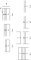
Figures 2a to 2g show an example schematic illustration of a cross section of a plurality of stacks resulting from the steps of the process flowchart offigure 1 . -
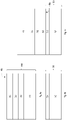
Figures 3a to 3c show an example cross section schematic illustration of a stack, a target substrate, and the bonding step of the stack to the target substrate. -
Figures 4a to 4c show a second example cross section schematic illustration of a stack, a target substrate, and the bonding step of the stack to the target substrate. -
Figures 5a to 5c show a third example cross section schematic illustration of a stack, a target substrate, and the bonding step of the stack to the target substrate. -
Figure 1 shows an example schematic illustration of a process flowchart of transferring a target layer to a target substrate, comprising the steps of:
In step a, astack 100 is formed by: - i. forming a
first transfer layer 20 over afirst substrate 10, - ii. forming a
second transfer layer 30 over thefirst transfer layer 20, thesecond transfer layer 30 being water-soluble, - iii. forming the
target layer 40 on thesecond transfer layer 30, and wherein thestack 100 has atop surface 40a. - In step b, the
top surface 40a of thestack 100 is bonded to asecond substrate 50. - In step c, the
first transfer layer 20 is separated from thesecond transfer layer 30. - In step d, the
second transfer layer 30 is dissolved in water. - The steps in
Figure 1 are further illustrated with the help ofFigures 2a to 5c . InFigure 2a , thefirst transfer layer 20 is deposited above thefirst substrate 10. - According to an example embodiment, the
first transfer layer 20 is a polymer layer formed on thefirst substrate 10, for example, by spin coating. - In
Figure 2b , the water solublesecond transfer layer 30 is deposited on thefirst substrate 20. According to an example embodiment, thesecond transfer layer 30 is dissolvable in water at room temperature. According to an example embodiment, thesecond transfer layer 30 is a polymer layer dissolvable in water at room temperature, for example, but not limited to, an Poly(vinyl alcohol) (PVOH, PVA, or PVAI) layer. According to an example embodiment, thesecond transfer layer 30 has a thickness of less than 10 µm, for example 0.8 µm. - In
Figure 2c , thetarget layer 40 is deposited above the water solublesecond transfer layer 30, having atop surface 40a. According to an example embodiment, thetarget layer 40 is a chemically and/or physically weak layer. The target layer may comprise materials that range from inorganic layers such as III-V materials, dielectrics, quantum dots to organics layers such as soft polymers, organic semiconductors, living cells and so on. Fragile layers of those materials can be advantageously transferred regardless of the weak physical constraints of the materials (chemical, mechanical, optical and/or thermal), and/or process-introduced physical constraints, including for example chemical, mechanical, optical and/or thermal constraints. According to an example embodiment, the target layer comprises anelastomer layer 42. Theelastomer layer 42 may have a Young's modulus equal or less than 500Mpa at room temperature 300K, preferably equal to or less than 100MPa at room temperature. According to an example embodiment, theelastomer layer 42 is formed by spin coating. According to an example embodiment, the thickness of theelastomer layer 42 is equal to or less than 100 µm, preferably equal to or less than 15µm. - According to an example embodiment, the
target layer 40 comprises anelastomer layer 42 and aconductive layer 44. According to an example embodiment, as shown inFigure 3a , theconductive layer 44 is deposited before theelastomer layer 42. According to another example embodiment, theconductive layer 44 is deposited after theelastomer layer 42, which is not shown in the figures. According to another example embodiment, which is not shown in the figures, thetarget layer 40 comprises multiple layers such as a plurality of elastomer layers, a plurality of conductive layers and/or combination. According to an example embodiment, theconductive layer 44 comprises a thin film metal layer. The metal layer may be a layer of metal, for example aluminum (Al), copper (Cu), iron (Fe) or an alloy thereof. According to an example embodiment, theconductive layer 44 comprises an inorganic layer. The inorganic layer may comprise silicon (Si), III-V material, 2-dimensional material and/or another conductive non-metallic material. According to an example embodiment, theconductive layer 44 has a thickness of equal to or less than 100 nm. - According to an example embodiment, the
conductive layer 44 is a thin film metal layer, an inorganic layer, or a combination thereof. According to an example, theconductive layer 44 is formed by for example chemical vapor deposition (CVD), physical vapor deposition (PVD), atom layer deposition (ALD), etc. - According to an example embodiment, which is not shown in the figures, the method may further comprise a step of patterning of at least one layer, the conductive layer and/or the elastomer layer, of the
target layer 40 before step b to form electronic connections/circuits. - In
Figure 2d ,3c ,4c and5c , thetop surface 40a of thestack 100 is bonded to thesecond substrate 50. - According to an example embodiment the
second substrate 50 comprises a semiconductor substrate, such as silicon, GaN or other semiconductor material. Thesecond substrate 50 may also comprise aglass supporting substrate 52 which is preferred in microfluidic devices for possible optical inspection. According to an example embodiment, thesecond substrate 50 may comprise anelastomer layer 54 formed by spin coating. According to an example embodiment, as shown inFigure 4b , the second substrate comprises anelastomer layer 54 above a supportingsubstrate 52. Theelastomer layer 54 may be patterned before step b infigure 1 . According to an example embodiment, theelastomer layer 54 may be of the same type as theelastomer layer 42. According to an example embodiment, theelastomer layer 54 is patterned to form at least a channel configured for microfluidic flow. According to an example embodiment, thesecond substrate 50 may comprise a semiconductor circuit layer. In a preferred embodiment, as shown inFigure 5b , the semiconductor circuit layer is a thin-film layer 56 configured as electronic circuit by patterning processes. According to an example embodiment, the patterning uses lithography technology. According to an example embodiment, theelastomer layer 54 is formed above the thin-film layer 56. - In
Figure 2e , thefirst transfer layer 20 is separated from thesecond transfer layer 30. The separation may be done by a thermal process. According to an example embodiment, thefirst transfer layer 20 can be a thermal sensitive layer where the chemical properties of thefirst transfer layer 20 is changed when exposed to a heat source. The separation may be alternatively done by exposure to a laser source. According to another example embodiment, thefirst transfer layer 20 is an optical sensitive layer where the chemical properties of thefirst transfer layer 20 is changed when exposed to a laser source of certain wavelength. Thefirst substrate 10 is transparent so that, thefirst transfer layer 20 can be separated from thesecond transfer layer 30 by exposure to the laser source. Being transparent means that the laser with a certain wavelength, for example 248nm, can be transmitted through thefirst substrate 10. When the separation is in progress, thesecond transfer layer 30 advantageously functions as a protective layer to protect thefragile target layer 40. - In
Figure 2f , thesecond transfer layer 30 is dissolved in water. The process is preferably done at room temperature to further limit damage or impact on thetransfer layer 30. According to an example, one side of thesecond transfer layer 30 is completely exposed to water. According to an example, because of the large exposure area of thesecond transfer layer 30, step c infigure 1 only takes less than 1 minute to remove thesecond transfer layer 30 with a thickness of 0.8 µm in the case of transferring thetarget layer 40 to the second substrate. - In
Figure 2g , thefragile target layer 40 is efficiently and successfully transferred to thesecond substrate 50. - According to an example embodiment, the transferring method is applicable for die to die, wafer to wafer or roll to roll transfer due to the large exposure area of the
second transfer layer 30 to water. - According to an example embodiment, which is not shown in the figures, the method further comprises a step of patterning of at least one layer in the
target layer 40 after step d infigure 1 to form for example electronic connections/circuits. - According to an example embodiment, the process of lithography, bonding, debonding and patterning are conventional CMOS (Complementary metal-oxide-semiconductor) technology processes.
Claims (12)
- A method for transferring a target layer (40) to a substrate comprising:a. providing a stack (100) by:i. forming a first transfer layer (20) over a first substrate (10),ii. forming a second transfer layer (30) on the first transfer layer (20), the second transfer layer (30) being water-soluble,iii. forming the target layer (40) on the second transfer layer (30), and wherein the stack (100) has a top surface (40a);b. bonding the top surface (40a) of the stack (100) to a second substrate (50);c. separating the first transfer layer (20) from the second transfer layer (30); andd. dissolving the second transfer layer (30) in water.
- A method according to claim I, wherein the second transfer layer is capable of dissolving at room temperature.
- A method according to claim 2, wherein the target layer (40) comprises an elastomer layer (42).
- A method according to claim 3, wherein the elastomer layer (42) has a Young's modulus equal to or less than 500MPa at room temperature.
- A method according to claim 3 or 4, wherein the target layer (40) further comprises a conductive layer (44).
- A method according to claim 5, wherein the conductive layer (44) is formed before the elastomer layer (42).
- A method according to claim 5 or 6, wherein the conductive layer (44) is a thin film metal layer or an inorganic layer.
- A method according to any of the preceding claims, wherein the second substrate (50) comprises a glass supporting substrate (52).
- A method according to any of the preceding claims, wherein the second substrate (50) comprises a patterned elastomer layer (54) comprising a channel configured for microfluidic flow.
- A method according to any of the preceding claims, wherein the second substrate (50) comprises a thin-film layer (56) configured for comprising electronic circuitry.
- A method according to any of the preceding claims, wherein the first substrate (10) is transparent and wherein the first transfer layer (20) is an optical sensitive layer and wherein the second transfer layer (30) is separated from the first transfer layer (20) by exposing to a laser source in step c.
- A method according to any of the preceding claims, wherein the method is compatible with CMOS technology.
Priority Applications (2)
| Application Number | Priority Date | Filing Date | Title |
|---|---|---|---|
| EP21178581.1A EP4102543A1 (en) | 2021-06-09 | 2021-06-09 | A method for transferring a layer to a substrate |
| US17/834,413 US12214580B2 (en) | 2021-06-09 | 2022-06-07 | Method for transferring a layer to a substrate |
Applications Claiming Priority (1)
| Application Number | Priority Date | Filing Date | Title |
|---|---|---|---|
| EP21178581.1A EP4102543A1 (en) | 2021-06-09 | 2021-06-09 | A method for transferring a layer to a substrate |
Publications (1)
| Publication Number | Publication Date |
|---|---|
| EP4102543A1 true EP4102543A1 (en) | 2022-12-14 |
Family
ID=76392144
Family Applications (1)
| Application Number | Title | Priority Date | Filing Date |
|---|---|---|---|
| EP21178581.1A Pending EP4102543A1 (en) | 2021-06-09 | 2021-06-09 | A method for transferring a layer to a substrate |
Country Status (2)
| Country | Link |
|---|---|
| US (1) | US12214580B2 (en) |
| EP (1) | EP4102543A1 (en) |
Citations (3)
| Publication number | Priority date | Publication date | Assignee | Title |
|---|---|---|---|---|
| US20090261062A1 (en) * | 2008-04-17 | 2009-10-22 | Myung-Hwan Kim | Carrier substrate and method of manufacturing flexible display apparatus using the same |
| US20170170003A1 (en) * | 2015-12-11 | 2017-06-15 | Suss Microtec Photonic Systems Inc. | Sacrificial layer for post-laser debris removal systems and methods |
| WO2021095480A1 (en) * | 2019-11-14 | 2021-05-20 | 株式会社朝日Fr研究所 | Bioelectrode, production method and installation method for bioelectrode |
Family Cites Families (3)
| Publication number | Priority date | Publication date | Assignee | Title |
|---|---|---|---|---|
| JP3809733B2 (en) * | 1998-02-25 | 2006-08-16 | セイコーエプソン株式会社 | Thin film transistor peeling method |
| WO2017192749A1 (en) * | 2016-05-03 | 2017-11-09 | Ultra Small Fibers, LLC | Semipermeable ultrathin polymer membranes |
| EP3825003B1 (en) * | 2019-11-21 | 2022-06-01 | Imt Ag | Method for manufacturing a microfluidic device |
-
2021
- 2021-06-09 EP EP21178581.1A patent/EP4102543A1/en active Pending
-
2022
- 2022-06-07 US US17/834,413 patent/US12214580B2/en active Active
Patent Citations (3)
| Publication number | Priority date | Publication date | Assignee | Title |
|---|---|---|---|---|
| US20090261062A1 (en) * | 2008-04-17 | 2009-10-22 | Myung-Hwan Kim | Carrier substrate and method of manufacturing flexible display apparatus using the same |
| US20170170003A1 (en) * | 2015-12-11 | 2017-06-15 | Suss Microtec Photonic Systems Inc. | Sacrificial layer for post-laser debris removal systems and methods |
| WO2021095480A1 (en) * | 2019-11-14 | 2021-05-20 | 株式会社朝日Fr研究所 | Bioelectrode, production method and installation method for bioelectrode |
Non-Patent Citations (2)
| Title |
|---|
| BOWEN JI ET AL.: "Stretchable Parylene-C electrodes enabled by serpentine structures on arbitrary elastomers by silicone rubber adhesive", JOURNAL OF MATERIOMICS, vol. 6, 2020, pages 330 - 338 |
| JIYOON NAM ET AL.: "Transfer Printed Flexible and Stretchable Thin Film Solar Cells Using a Water-Soluble Sacrificial Layer", ADV. ENERGY MATER., 2016, pages 1601269 |
Also Published As
| Publication number | Publication date |
|---|---|
| US20220396067A1 (en) | 2022-12-15 |
| US12214580B2 (en) | 2025-02-04 |
Similar Documents
| Publication | Publication Date | Title |
|---|---|---|
| US20230115122A1 (en) | Method of bonding thin substrates | |
| Baca et al. | Printable single‐crystal silicon micro/nanoscale ribbons, platelets and bars generated from bulk wafers | |
| US8735260B2 (en) | Method to prevent metal pad damage in wafer level package | |
| US10460971B2 (en) | Multi-chip package assembly | |
| US8963278B2 (en) | Three-dimensional integrated circuit device using a wafer scale membrane | |
| EP2530709B1 (en) | Method of producing a semiconductor wafer | |
| US20100273286A1 (en) | Method Of Fabricating An Integrated CMOS-MEMS Device | |
| US7943440B2 (en) | Fabrication method of thin film device | |
| TWI475618B (en) | Wafer-level packaging semiconductor method | |
| CN111199951A (en) | Semiconductor device, manufacturing method thereof and manufacturing method of alignment mark | |
| KR102793647B9 (en) | Deposition masks and methods of manufacturing and using deposition masks | |
| US20100330506A1 (en) | Method for transferring an epitaxial layer from a donor wafer to a system wafer appertaining to microsystems technology | |
| US12214580B2 (en) | Method for transferring a layer to a substrate | |
| TWI354325B (en) | ||
| EP3796406B1 (en) | Method of manufacturing electronic device | |
| KR20220161331A (en) | Methods and Systems for Forming Metal Interconnect Layers Using Machined Templates | |
| US12002792B2 (en) | Method and system for transferring alignment marks between substrate systems | |
| Landesberger et al. | Ultra-thin wafer fabrication through dicing-by-thinning | |
| KR20100096948A (en) | Fabrication method of thin film device | |
| EP4564404A1 (en) | A method for removing residues from a substrate surface | |
| CN110137345A (en) | A kind of magnetic sensor and preparation method thereof | |
| CN112820655B (en) | Semiconductor device packaging method | |
| US20060084238A1 (en) | Method for bonding wafers | |
| KR101339291B1 (en) | Flexible interated circuit and method of manufacturing the flexible interated circuit | |
| CN118974915A (en) | Method for forming a semiconductor package using dielectric alignment marks and a laser lift-off process |
Legal Events
| Date | Code | Title | Description |
|---|---|---|---|
| PUAI | Public reference made under article 153(3) epc to a published international application that has entered the european phase |
Free format text: ORIGINAL CODE: 0009012 |
|
| STAA | Information on the status of an ep patent application or granted ep patent |
Free format text: STATUS: THE APPLICATION HAS BEEN PUBLISHED |
|
| AK | Designated contracting states |
Kind code of ref document: A1 Designated state(s): AL AT BE BG CH CY CZ DE DK EE ES FI FR GB GR HR HU IE IS IT LI LT LU LV MC MK MT NL NO PL PT RO RS SE SI SK SM TR |
|
| STAA | Information on the status of an ep patent application or granted ep patent |
Free format text: STATUS: REQUEST FOR EXAMINATION WAS MADE |
|
| 17P | Request for examination filed |
Effective date: 20230613 |
|
| RBV | Designated contracting states (corrected) |
Designated state(s): AL AT BE BG CH CY CZ DE DK EE ES FI FR GB GR HR HU IE IS IT LI LT LU LV MC MK MT NL NO PL PT RO RS SE SI SK SM TR |
|
| REG | Reference to a national code |
Ref country code: DE Ref legal event code: R079 Free format text: PREVIOUS MAIN CLASS: H01L0021020000 Ipc: H10P0072000000 |
|
| GRAP | Despatch of communication of intention to grant a patent |
Free format text: ORIGINAL CODE: EPIDOSNIGR1 |
|
| STAA | Information on the status of an ep patent application or granted ep patent |
Free format text: STATUS: GRANT OF PATENT IS INTENDED |
|
| RIC1 | Information provided on ipc code assigned before grant |
Ipc: H10P 72/00 20260101AFI20260302BHEP Ipc: H10P 90/00 20260101ALI20260302BHEP |
|
| INTG | Intention to grant announced |
Effective date: 20260401 |